US4705332A - High density, controlled impedance connectors - Google Patents
High density, controlled impedance connectorsDownload PDFInfo
- Publication number
- US4705332A US4705332AUS07/016,968US1696887AUS4705332AUS 4705332 AUS4705332 AUS 4705332AUS 1696887 AUS1696887 AUS 1696887AUS 4705332 AUS4705332 AUS 4705332A
- Authority
- US
- United States
- Prior art keywords
- conductive
- high density
- wafers
- stack
- electrical connector
- Prior art date
- Legal status (The legal status is an assumption and is not a legal conclusion. Google has not performed a legal analysis and makes no representation as to the accuracy of the status listed.)
- Expired - Fee Related
Links
- 235000012431wafersNutrition0.000claimsabstractdescription98
- 125000006850spacer groupChemical group0.000claimsdescription10
- 239000004020conductorSubstances0.000claimsdescription7
- 239000003989dielectric materialSubstances0.000claimsdescription7
- 239000000463materialSubstances0.000claimsdescription2
- 239000012774insulation materialSubstances0.000description2
- 229920002492poly(sulfone)Polymers0.000description2
- 230000000717retained effectEffects0.000description2
- RYGMFSIKBFXOCR-UHFFFAOYSA-NCopperChemical compound[Cu]RYGMFSIKBFXOCR-UHFFFAOYSA-N0.000description1
- 229910045601alloyInorganic materials0.000description1
- 239000000956alloySubstances0.000description1
- 230000005540biological transmissionEffects0.000description1
- 229910052802copperInorganic materials0.000description1
- 239000010949copperSubstances0.000description1
- 238000003780insertionMethods0.000description1
- 230000037431insertionEffects0.000description1
- 239000011810insulating materialSubstances0.000description1
- 238000002955isolationMethods0.000description1
- 239000012858resilient materialSubstances0.000description1
- 239000000758substrateSubstances0.000description1
Images


Classifications
- H—ELECTRICITY
- H01—ELECTRIC ELEMENTS
- H01R—ELECTRICALLY-CONDUCTIVE CONNECTIONS; STRUCTURAL ASSOCIATIONS OF A PLURALITY OF MUTUALLY-INSULATED ELECTRICAL CONNECTING ELEMENTS; COUPLING DEVICES; CURRENT COLLECTORS
- H01R13/00—Details of coupling devices of the kinds covered by groups H01R12/70 or H01R24/00 - H01R33/00
- H01R13/648—Protective earth or shield arrangements on coupling devices, e.g. anti-static shielding
- H01R13/658—High frequency shielding arrangements, e.g. against EMI [Electro-Magnetic Interference] or EMP [Electro-Magnetic Pulse]
- H01R13/6581—Shield structure
- H01R13/6585—Shielding material individually surrounding or interposed between mutually spaced contacts
- H01R13/6586—Shielding material individually surrounding or interposed between mutually spaced contacts for separating multiple connector modules
- H—ELECTRICITY
- H01—ELECTRIC ELEMENTS
- H01R—ELECTRICALLY-CONDUCTIVE CONNECTIONS; STRUCTURAL ASSOCIATIONS OF A PLURALITY OF MUTUALLY-INSULATED ELECTRICAL CONNECTING ELEMENTS; COUPLING DEVICES; CURRENT COLLECTORS
- H01R12/00—Structural associations of a plurality of mutually-insulated electrical connecting elements, specially adapted for printed circuits, e.g. printed circuit boards [PCB], flat or ribbon cables, or like generally planar structures, e.g. terminal strips, terminal blocks; Coupling devices specially adapted for printed circuits, flat or ribbon cables, or like generally planar structures; Terminals specially adapted for contact with, or insertion into, printed circuits, flat or ribbon cables, or like generally planar structures
- H—ELECTRICITY
- H01—ELECTRIC ELEMENTS
- H01R—ELECTRICALLY-CONDUCTIVE CONNECTIONS; STRUCTURAL ASSOCIATIONS OF A PLURALITY OF MUTUALLY-INSULATED ELECTRICAL CONNECTING ELEMENTS; COUPLING DEVICES; CURRENT COLLECTORS
- H01R13/00—Details of coupling devices of the kinds covered by groups H01R12/70 or H01R24/00 - H01R33/00
- H01R13/648—Protective earth or shield arrangements on coupling devices, e.g. anti-static shielding
- H01R13/658—High frequency shielding arrangements, e.g. against EMI [Electro-Magnetic Interference] or EMP [Electro-Magnetic Pulse]
- H01R13/6591—Specific features or arrangements of connection of shield to conductive members
- H01R13/6597—Specific features or arrangements of connection of shield to conductive members the conductive member being a contact of the connector
- H—ELECTRICITY
- H01—ELECTRIC ELEMENTS
- H01R—ELECTRICALLY-CONDUCTIVE CONNECTIONS; STRUCTURAL ASSOCIATIONS OF A PLURALITY OF MUTUALLY-INSULATED ELECTRICAL CONNECTING ELEMENTS; COUPLING DEVICES; CURRENT COLLECTORS
- H01R12/00—Structural associations of a plurality of mutually-insulated electrical connecting elements, specially adapted for printed circuits, e.g. printed circuit boards [PCB], flat or ribbon cables, or like generally planar structures, e.g. terminal strips, terminal blocks; Coupling devices specially adapted for printed circuits, flat or ribbon cables, or like generally planar structures; Terminals specially adapted for contact with, or insertion into, printed circuits, flat or ribbon cables, or like generally planar structures
- H01R12/70—Coupling devices
- H01R12/71—Coupling devices for rigid printing circuits or like structures
- H01R12/72—Coupling devices for rigid printing circuits or like structures coupling with the edge of the rigid printed circuits or like structures
- H01R12/721—Coupling devices for rigid printing circuits or like structures coupling with the edge of the rigid printed circuits or like structures cooperating directly with the edge of the rigid printed circuits
Definitions
- the present inventionrelates to a high density, controlled impedance connector and, more particularly, to a high density connector which may be utilized to mate a plurality of modules (daughter boards) to a backplane (mother board) wherein each electrical connection has a controlled impedance and a minimum amount of crosstalk.
- a flat cable formed with a plurality of flat conductors and surrounded on its upper and lower surface by a ground plane, thus forming a striplinemay be found in U.S. Pat. No. 3,612,744, issued Oct. 12, 1971 and invented by P. J. Thomas.
- a second flat cable in the form of a microstripis described in U.S. Pat. No. 4,441,088, which issued Apr. 3, 1984 by C. J. Anderson.
- the Anderson patentdiscusses the reduction of crosstalk by adjusting the amount of dielectric material between the flat conductor and the ground plane in proportion to the amount of dielectric material placed over the flat conductor.
- a later connector for shielding electrical contacts therein to permit a high frequency signal to pass there through utilizing a stripline configurationis shown in an IBM Technical Disclosure Bulletin, Volume 10, No. 3, August 1967, pp. 203-4. This connector does not contemplate a high density connector as in the present invention.
- a further objectis to provide a high density connector which may be easily configured to accommodate different sized printed circuit boards and different mounting configurations.
- Yet a further objectis to provide a configuration for an electrical connector which may be easily replaced and repaired.
- a still further object of this inventionis to provide a high density, controlled impedance connector, which is economic, flexible and expandable.
- a discrete waferformed from a dielectric material having a plurality of conductive elements mounted by said wafer.
- a single, ground plane element for connection to an electrical groundis also mounted by the wafer.
- the discrete wafersare then stacked side-by-side in an arrangement which permits the ground plane, mounted by two wafers, to surround the plurality of conductive elements, mounted by a single discrete wafer. This arrangement creates a stripline configuration for the plurality of conductive elements, whose configuration controls the impedance of the conductive elements.
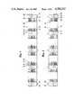
- FIG. 1is a side view showing an alternative embodiment of a high density connector incorporating the present invention
- FIG. 2is an end view of FIG. 1;
- FIG. 3is a bottom plane view of FIG. 1;
- FIG. 4is an exploded, perspective view, showing the connector illustrated in FIGS. 1-3;
- FIG. 5is a cross sectional view showing the high density connector mounting four daughter boards upon a mother board
- FIG. 6shows a typical layout for the conductive pads which may be utilized upon a mother board or a daughter board, mounting the connectors shown in FIGS. 1-5;
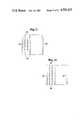
- FIG. 7is a perspective view showing an insulated discrete wafer utilized within a preferred embodiment of the present invention.
- FIG. 8is a cross-sectional view taken along line 8--8 of FIG. 7;
- FIG. 9is a cross-sectional view of a high density connector incorporating the wafer shown in FIGS. 7 and 8;
- FIG. 10is a cross-sectional view of the second side of the wafer shown in FIG. 9;
- FIG. 11is a side view, similar to FIG. 1, illustrating the preferred embodiment of a high density connector incorporating the features of the present invention
- FIG. 12is an end view of FIG. 11;
- FIG. 13is a bottom plan view of the connector shown in FIG. 11;
- FIG. 14is a perspective view showing an insulating housing which receives the discrete wafers of FIG. 7;
- FIG. 15is a partial view showing the conductive pads, which may be utilized upon a printed circuit board mounting the connector shown in FIGS. 7-14;
- FIG. 16is a cross-sectional view taken along line 16--16 of FIG. 9;
- FIG. 17is a cross-sectional view taken along line 17--17 of FIG. 9;
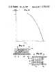
- FIG. 18is a curve showing the maximum crosstalk as a percentage versus the pitch to height ratio (P/H) of the connector
- FIG. 19is a schematic representation, similar to FIG. 12, showing a connector arrangement wherein the printed circuit boards may be mounted in a parallel and aligned configuration;
- FIG. 20is a schematic, similar to FIG. 19, presenting a connector mounting arrangement wherein the printed circuit boards may be mounted in parallel;
- FIG. 21shows a schematic arrangement of the plurality of conductive elements shown in the connector of FIGS. 7-14.
- FIG. 22is a schematic representation similar to FIG. 21 showing another embodiment.
- FIGS. 1-5illustrate one embodiment of the high density connector 10 wherein FIG. 1 is a side view showing various components of the connector including a discrete wafer 12 which, in this alternative embodiment, mounts a plurality of signal carrying contact elements 14 adjacent to which is mounted a single ground plane element 16.
- a discrete wafer 12which, in this alternative embodiment, mounts a plurality of signal carrying contact elements 14 adjacent to which is mounted a single ground plane element 16.
- Each discrete wafer 12is placed in a side-by-side stack with other discrete wafers 12 having ground plane elements 16 placed therebetween as best seen in FIG. 4.
- the individual contact elements 12are encapsulated within the insulating, dielectric material of wafer 14 and surrounded on each side by ground planes 16 for creating a stripline arrangement for each contact element 14.
- the individual contact elements 14are fabricated to form a ninety degree turn (FIG. 5) which is terminated at each end by a pair of spring wiping finger 18.
- the ground plane elements 16are each provided with four spring wiping fingers 19 (FIG. 4).
- the spring fingers 18 and 19are bent at an angle to the right in FIGS. 1, 2 and 4 with fingers 18 extending from each wafer 12 at a surface which has been recessed at 20 to permit flexure in the right-hand direction.
- the right-hand flexure of the spring fingers 18 and 19fits over adjacent spring fingers so that a high density of these fingers may be accommodated within the side-by-side stack of wafers 12.
- a spacer 22is provided at the far right edge of each stack, followed by a mounting bracket 24.
- the ground plane element 16 and spacers 22have a configuration similar to the configuration of wafer 12 which includes a recess 23. It may now be seen that the purpose of the spacer 22 and its recess 23 is to provide an area into which the spring fingers 18 and 19 may flex when the connector 10 is assembled against a printed circuit board.
- the addition of the mounting brackets 24 on opposite sides of the wafer stackcompletes the assembly.
- the wafers 12, ground plane elements 16, spacers 22 and mounting brackets 24are assembled in a stack which may be formed by a series of repeated parts to any desired length. These parts are provided with a plurality of apertures including three smaller apertures 25 for receiving a set of locating shafts 26 and a larger aperture 27 for receiving a support shaft 28.
- the connector 10is thus assembled by stacking a mounting bracket 24 on the left-hand end of the stack followed by a ground plane element 16, a wafer 12, and a ground plane element 16 until a predetermined number of wafers and ground plane elements have been stacked upon the shafts 26 and 28. It should be noted here that the number of ground plane elements 16 is one more than the wafers 12.
- the stackis then followed by a spacer 22 which provides the recesses 23 into which the spring fingers 18 for contacts 14 and spring fingers 19 for ground plane 16 extend.
- the next element in the stackis a second mounting bracket 24.
- the stackis typically 12" ⁇ 1/2 ⁇ 1/2" in size.
- the support shaft 28receives a screw 30 at each end whose threads pass through a clearance hole in bracket 24 into the internally threaded end of shaft 28 for compressing and retaining the 12" stack in its desired configuration.
- each bracket 24having four locating pins 32 extending from two adjacent surfaces.
- a first surfacemounts a backplane or mother board 34 wherein locating pins 32 are received by apertures 36 within the board 34.
- Mounted at a right angle, or ninety degrees to the mother board 34is a module or daughter board 38, also having apertures 36 therein for receiving the locating pins 32.
- the mother and daughter boards 34 and 38are retained against the connector 10 by suitable fastening means, such as screws 40.
- suitable fastening meanssuch as screws 40.
- the screws 40pass through the boards 34 and 38 into threaded holes in the mounting brackets 24.
- the wafers 12are illustrated with the contact elements 14 encapsulated therein. It will be understood that the spring fingers 18 of contact elements 14 are compressed against the mother and daughter boards 34 and 38 within the recesses 20 to make an electrical connection therebetween.
- the spring fingers 18contact suitable pads 42 such as those shown in FIG. 6 mounted upon the daughter board 38. Each individual pad 42 is provided with apertures 44 to make an electrical connection to the far side of the daughter board where connection with electrical conductors (not shown) is completed.
- the spring fingers 19 on the ground plane elements 16contact a pair of conductive strips 46 on either side of the pads 42.
- the connector 10consists of a stack of five brackets 24, four spacers 22, two hundred and four wafers 12 and two hundred and eight ground planes 14.
- the readerwill remember that, in the embodiment shown, there are four substacks of wafers 12 so that the one additional ground plane 16 in each substack totals the four additional ground planes in the completed stack.
- the arrangement shownprovides for eight hundred and sixteen signal contacts made by spring fingers 18 and four hundred and sixteen ground contacts made by fingers 19.
- FIGS. 7-14A preferred embodiment of the present invention is shown in FIGS. 7-14.
- a discrete dielectric wafer 52is molded from suitable insulation materials, such as polysulfone, to mount a plurality of individual conductive contact elements 54, FIG. 9, on one side, and to mount a single ground plane element 56 on the other side thereof, FIG. 10.
- Each individual signal contact 54is constructed with an arcuate curve of ninety degrees which is terminated at each end by a spring wiping fingers 58.
- the spring fingers 58are shown in their compressed position in FIGS. 9 and 10 as if pressed against a printed circuit board such as boards 34 or 38.
- the ground plane element 56is also provided with a plurality of spring fingers 59, which coincide in their spacing with each individual spring finger 58 from the contact elements 54.
- the contact elements 54 and ground plane elements 56may be constructed from beryllum copper or other suitable alloys.
- the dielectric wafer 52is molded into a hexagonal shape having first and second generally flat surfaces 60 and 62 (FIG. 7).
- the first surface 60is provided with a plurality of grooves 64, eight are shown in the preferred embodiment of FIG. 8, which receive the arcuate contact elements 54.
- Two edges of surface 60, arranged at right angles to one another,are relieved to a depth equal to the depth of grooves 64 to form recesses 66. These recesses 66 provide clearance for the motion of the spring fingers 58 as they are pressed against the printed circuit boards.
- the second surface 62 of wafer 52is provided with a single recess 68 which receives the ground plane element 56. Recess 68 extends to the two edges of the hexagonal wafer 52 that are arranged at ninety degrees to one another to permit the spring fingers 59 of the ground plane element 56 to be exposed to the printed circuit boards opposite fingers 58.
- the discrete wafers 52 with the contacts 54 and ground plane 56 in placemay be stacked in a side-by-side arrangement to create a stack that forms the high density connector 50. It is possible to form the grooves 64 deep enough within the surfaces 60 of wafers 52 to place one wafer against the other without causing the contact elements 54 to touch the adjacent ground plane 56.
- a slotted housing 72is provided to receive that discrete wafers 52. Housing 72, FIG. 14, has a hexagonal cross section and is molded from a suitable insulated material, such as polysulfone, with a plurality of slots 74 which are open along two edge surfaces arranged at a right angle to one another.
- the slots 74are arranged to receive the wafers 52, contact elements 54, and ground planes 56.
- the housing 72thus forms a first housing for mounting the plurality of wafers 52. Housing 72 is then inserted into an elongated opening 76 in the second housing 78. The insertion of first housing 72 into elongated openings 76 may be accomplished by removing the top of housing 78. However, in the preferred embodiment, a pie shaped piece 79 is removed. Housing 72 is then rotated slightly and inserted into opening 76 so as not to injure the spring fingers 58 and 59. By rotating the housing 72, it is possible to insert the housing 72 into slot 76 far enough to permit the clearance of contacts 58 and 59 into the left-hand opening of slot 76.
- the wedge member 79may be replaced and retained by suitable fastening means, such as screws, not shown.
- the second housing 78is provided with locating pins 80 and threaded apertures 81 for aligning and mounting the connector 50 to suitable printed circuit boards 82 and 84, or by screws 85, FIG. 12.
- the stack of wafers 52comprises a ground plane 56 at the far left-hand end of the slot 76 adjacent housing 72.
- the ground planeis mounted by the wafer 52 whose next surface mounts the contact elements 54.
- This alternate stackcontinues until the far right-hand end of slot 76 wherein the last wafer 52 includes only the ground plane 56.
- slot 76may mount one hundred and one wafers 52 therein having one hundred sets of contact elements 54 and one hundred and one sets of ground plane elements 56.
- This configurationmounts a total of sixteen hundred and eight spring finger contacts 54 and 56.
- the spring fingers 54 and 56are shown schematically in FIGS. 11 and 13 as simple dots.
- the spring fingers 58 of contact elements 54slide across pads 86 (FIG. 15) to make electrical contact with the board 82.
- the spring fingers 59 of the ground plane elements 56slide across conductive strips 88 to complete the stripline circuit formed by surrounding contact elements 54 by ground planes 56.
- each contact 54has been formed with the side-by-side ground planes 56 equal distance from the contacts 54.
- the ground planes 56are separated by a distance "b” whereas the contact elements 54 having a width "w” and a thickness "t” are spaced from the bottom ground plane 56 by a distance "H”.
- the contacts 54are spaced apart by a pitch "P”.
- the impedance Z o of each contact 54may be expressed by the equation: ##EQU1## wherein:
- Crosstalk within connector 50may be reduced by providing a thicker spring finger 59 for each ground plane 56 than the related spring finger 58 for each contact 54. This configuration is shown in FIG. 17. Crosstalk may also be reduced by adjusting the ratio of the distance between two adjacent contact elements 54 or pitch "P" in proportion to the height "H" of the contacts 54 above the ground plane 56. The percentage of reduction of crosstalk versus the pitch to height ratio (P/H) is shown in FIG. 18. By adjusting the pitch of the contact elements 54 or the equal spacing of these contacts from the ground planes 56, it is possible to reduce crosstalk significantly as shown by the curve of FIG. 18.
- the connector 50 and its housing 78may be modified wherein the contacts 54 extend through a 180 degree arc to mount the two boards 82 and 84 in a parallel in-line configuration, FIG. 19. Further, the connector 50 and its housing 78 may be modified to accommodate the contacts in a straight line configuration wherein the two boards 82 and 84 are mounted in a parallel configuration, one upon the other, FIG. 20.
- the preferred embodimentshas also shown the spring fingers 58 from the contact elements 54 mounted in alternating rows with fingers 59 from the ground planes element 56. Such an arrangement is shown schematically in FIG. 21. There are other embodiments, however, where it may be desirable to place the spring fingers 58 in an immediate side-by-side relationship separated by a pair of ground plane elements 56. Such an arrangement is shown in FIG. 22. This arrangement may be easily accomplished by the present invention.
Landscapes
- Details Of Connecting Devices For Male And Female Coupling (AREA)
- Coupling Device And Connection With Printed Circuit (AREA)
Abstract
Description
Claims (31)
Priority Applications (1)
| Application Number | Priority Date | Filing Date | Title |
|---|---|---|---|
| US07/016,968US4705332A (en) | 1985-08-05 | 1987-02-25 | High density, controlled impedance connectors |
Applications Claiming Priority (2)
| Application Number | Priority Date | Filing Date | Title |
|---|---|---|---|
| US76270685A | 1985-08-05 | 1985-08-05 | |
| US07/016,968US4705332A (en) | 1985-08-05 | 1987-02-25 | High density, controlled impedance connectors |
Related Parent Applications (1)
| Application Number | Title | Priority Date | Filing Date |
|---|---|---|---|
| US76270685AContinuation | 1985-08-05 | 1985-08-05 |
Publications (1)
| Publication Number | Publication Date |
|---|---|
| US4705332Atrue US4705332A (en) | 1987-11-10 |
Family
ID=26689284
Family Applications (1)
| Application Number | Title | Priority Date | Filing Date |
|---|---|---|---|
| US07/016,968Expired - Fee RelatedUS4705332A (en) | 1985-08-05 | 1987-02-25 | High density, controlled impedance connectors |
Country Status (1)
| Country | Link |
|---|---|
| US (1) | US4705332A (en) |
Cited By (59)
| Publication number | Priority date | Publication date | Assignee | Title |
|---|---|---|---|---|
| US4975084A (en)* | 1988-10-17 | 1990-12-04 | Amp Incorporated | Electrical connector system |
| WO1991001078A1 (en)* | 1989-07-05 | 1991-01-24 | Labinal Components & Systems, Inc. | Electrical connectors |
| US5066236A (en)* | 1989-10-10 | 1991-11-19 | Amp Incorporated | Impedance matched backplane connector |
| US5094623A (en)* | 1991-04-30 | 1992-03-10 | Thomas & Betts Corporation | Controlled impedance electrical connector |
| EP0644628A1 (en)* | 1993-09-17 | 1995-03-22 | Japan Aviation Electronics Industry, Limited | Electrical angle connector of a printed circuit board type having a plurality of connecting conductive strips of a common length |
| US5496183A (en)* | 1993-04-06 | 1996-03-05 | The Whitaker Corporation | Prestressed shielding plates for electrical connectors |
| US5522737A (en)* | 1992-03-24 | 1996-06-04 | Molex Incorporated | Impedance and inductance control in electrical connectors and including reduced crosstalk |
| US5597313A (en)* | 1986-06-19 | 1997-01-28 | Labinal Components And Systems, Inc. | Electrical connectors |
| US5672062A (en)* | 1991-01-30 | 1997-09-30 | Labinal Components And Systems, Inc. | Electrical connectors |
| US5702258A (en)* | 1996-03-28 | 1997-12-30 | Teradyne, Inc. | Electrical connector assembled from wafers |
| EP0852414A3 (en)* | 1997-01-07 | 1999-10-27 | Berg Electronics Manufacturing B.V. | Connector with integrated PCB assembly |
| US6015299A (en)* | 1998-07-22 | 2000-01-18 | Molex Incorporated | Card edge connector with symmetrical board contacts |
| US6083047A (en)* | 1997-01-16 | 2000-07-04 | Berg Technology, Inc. | Modular electrical PCB assembly connector |
| US6095821A (en)* | 1998-07-22 | 2000-08-01 | Molex Incorporated | Card edge connector with improved reference terminals |
| US6379188B1 (en) | 1997-02-07 | 2002-04-30 | Teradyne, Inc. | Differential signal electrical connectors |
| US6494734B1 (en) | 1997-09-30 | 2002-12-17 | Fci Americas Technology, Inc. | High density electrical connector assembly |
| US6524135B1 (en) | 1999-09-20 | 2003-02-25 | 3M Innovative Properties Company | Controlled impedance cable connector |
| US6746278B2 (en) | 2001-11-28 | 2004-06-08 | Molex Incorporated | Interstitial ground assembly for connector |
| US6824391B2 (en)* | 2000-02-03 | 2004-11-30 | Tyco Electronics Corporation | Electrical connector having customizable circuit board wafers |
| US6843657B2 (en) | 2001-01-12 | 2005-01-18 | Litton Systems Inc. | High speed, high density interconnect system for differential and single-ended transmission applications |
| US6910897B2 (en) | 2001-01-12 | 2005-06-28 | Litton Systems, Inc. | Interconnection system |
| US6979202B2 (en) | 2001-01-12 | 2005-12-27 | Litton Systems, Inc. | High-speed electrical connector |
| US20050283974A1 (en)* | 2004-06-23 | 2005-12-29 | Richard Robert A | Methods of manufacturing an electrical connector incorporating passive circuit elements |
| US20080146049A1 (en)* | 2006-12-19 | 2008-06-19 | Japan Aviation Electronics Industry, Limited | Connector excellent in high-frequency characteristics |
| US7549897B2 (en) | 2006-08-02 | 2009-06-23 | Tyco Electronics Corporation | Electrical connector having improved terminal configuration |
| US7591655B2 (en) | 2006-08-02 | 2009-09-22 | Tyco Electronics Corporation | Electrical connector having improved electrical characteristics |
| US20090298308A1 (en)* | 2004-06-23 | 2009-12-03 | Kenny William A | Electrical connector incorporating passive circuit elements |
| US7670196B2 (en) | 2006-08-02 | 2010-03-02 | Tyco Electronics Corporation | Electrical terminal having tactile feedback tip and electrical connector for use therewith |
| US7753742B2 (en) | 2006-08-02 | 2010-07-13 | Tyco Electronics Corporation | Electrical terminal having improved insertion characteristics and electrical connector for use therewith |
| US20100240233A1 (en)* | 2009-03-19 | 2010-09-23 | Johnescu Douglas M | Electrical connector having ribbed ground plate |
| WO2011076950A1 (en) | 2009-12-24 | 2011-06-30 | Fci Automotive Holding | Modular connector system |
| US8142236B2 (en) | 2006-08-02 | 2012-03-27 | Tyco Electronics Corporation | Electrical connector having improved density and routing characteristics and related methods |
| US20120129395A1 (en)* | 2010-11-19 | 2012-05-24 | Wayne Samuel Davis | Electrical Connector System |
| US8231415B2 (en) | 2009-07-10 | 2012-07-31 | Fci Americas Technology Llc | High speed backplane connector with impedance modification and skew correction |
| US8382524B2 (en) | 2010-05-21 | 2013-02-26 | Amphenol Corporation | Electrical connector having thick film layers |
| US8466365B2 (en) | 2010-08-31 | 2013-06-18 | 3M Innovative Properties Company | Shielded electrical cable |
| US8492655B2 (en) | 2010-08-31 | 2013-07-23 | 3M Innovative Properties Company | Shielded electrical ribbon cable with dielectric spacing |
| US8575491B2 (en) | 2010-08-31 | 2013-11-05 | 3M Innovative Properties Company | Electrical cable with shielding film with gradual reduced transition area |
| US8591257B2 (en) | 2011-11-17 | 2013-11-26 | Amphenol Corporation | Electrical connector having impedance matched intermediate connection points |
| US8658899B2 (en) | 2009-06-19 | 2014-02-25 | 3M Innovative Properties Company | Shielded electrical cable |
| US8734185B2 (en) | 2010-05-21 | 2014-05-27 | Amphenol Corporation | Electrical connector incorporating circuit elements |
| CN104009303A (en)* | 2013-02-26 | 2014-08-27 | 泰科电子公司 | Grounding structrues for contact modules of connector assemblies |
| US8841554B2 (en) | 2010-08-31 | 2014-09-23 | 3M Innovative Properties Company | High density shielded electrical cable and other shielded cables, systems, and methods |
| US8859901B2 (en) | 2010-09-23 | 2014-10-14 | 3M Innovative Properties Company | Shielded electrical cable |
| USD718253S1 (en) | 2012-04-13 | 2014-11-25 | Fci Americas Technology Llc | Electrical cable connector |
| US8905651B2 (en) | 2012-01-31 | 2014-12-09 | Fci | Dismountable optical coupling device |
| USD720698S1 (en) | 2013-03-15 | 2015-01-06 | Fci Americas Technology Llc | Electrical cable connector |
| US8944831B2 (en) | 2012-04-13 | 2015-02-03 | Fci Americas Technology Llc | Electrical connector having ribbed ground plate with engagement members |
| USD727268S1 (en) | 2012-04-13 | 2015-04-21 | Fci Americas Technology Llc | Vertical electrical connector |
| USD727852S1 (en) | 2012-04-13 | 2015-04-28 | Fci Americas Technology Llc | Ground shield for a right angle electrical connector |
| USD733662S1 (en) | 2013-01-25 | 2015-07-07 | Fci Americas Technology Llc | Connector housing for electrical connector |
| US9087649B2 (en) | 2012-08-22 | 2015-07-21 | Bae Systems Controls Inc. | Very low inductance distributed capacitive filter assembly |
| US9119292B2 (en) | 2010-08-31 | 2015-08-25 | 3M Innovative Properties Company | Shielded electrical cable in twinaxial configuration |
| USD746236S1 (en) | 2012-07-11 | 2015-12-29 | Fci Americas Technology Llc | Electrical connector housing |
| US9257778B2 (en) | 2012-04-13 | 2016-02-09 | Fci Americas Technology | High speed electrical connector |
| US9543703B2 (en) | 2012-07-11 | 2017-01-10 | Fci Americas Technology Llc | Electrical connector with reduced stack height |
| US9685259B2 (en) | 2009-06-19 | 2017-06-20 | 3M Innovative Properties Company | Shielded electrical cable |
| US10147522B2 (en) | 2010-08-31 | 2018-12-04 | 3M Innovative Properties Company | Electrical characteristics of shielded electrical cables |
| US12205732B2 (en) | 2010-08-31 | 2025-01-21 | 3M Innovative Properties Company | Shielded electric cable |
Citations (21)
| Publication number | Priority date | Publication date | Assignee | Title |
|---|---|---|---|---|
| US3184649A (en)* | 1961-08-18 | 1965-05-18 | Texas Instruments Inc | Miniature circuit assembly |
| US3209208A (en)* | 1961-08-14 | 1965-09-28 | Sippican Corp | Mounting assembly for modular electronic units |
| US3215968A (en)* | 1960-12-21 | 1965-11-02 | Adolf L Herrmann | Printed circuit board connector |
| US3270311A (en)* | 1962-07-12 | 1966-08-30 | Brown Engineering Company Inc | Connector for interconnecting printed circuit boards |
| US3401369A (en)* | 1966-06-07 | 1968-09-10 | Ibm | Connector |
| US3430182A (en)* | 1967-04-27 | 1969-02-25 | Nasa | Electrical feed-through connection for printed circuit boards and printed cable |
| US3493313A (en)* | 1967-07-31 | 1970-02-03 | Ronson Corp | Gas lighter |
| US3495134A (en)* | 1968-05-16 | 1970-02-10 | Ibm | Rota-pak system concept |
| US3601753A (en)* | 1970-06-10 | 1971-08-24 | Ibm | Coaxial interface connector |
| US3601772A (en)* | 1970-05-20 | 1971-08-24 | Berg Electronics Inc | Header block assembly |
| US3605068A (en)* | 1964-12-17 | 1971-09-14 | Western Electric Co | Electric coupler |
| US3612274A (en)* | 1969-04-21 | 1971-10-12 | Green Giant Co | Photoelectric food sorting method and apparatus |
| US3651432A (en)* | 1970-04-14 | 1972-03-21 | Amp Inc | Impedance matched printed circuit connectors |
| US3705332A (en)* | 1970-06-25 | 1972-12-05 | Howard L Parks | Electrical circuit packaging structure and method of fabrication thereof |
| US3780238A (en)* | 1971-12-27 | 1973-12-18 | Beckman Instruments Inc | Multi sectional rotary wafer switch assembly with improved support and terminal connector for thin circuit module |
| GB1410779A (en)* | 1971-09-28 | 1975-10-22 | Bendix Corp | Electrical connectors |
| US4070084A (en)* | 1976-05-20 | 1978-01-24 | Burroughs Corporation | Controlled impedance connector |
| US4232929A (en)* | 1978-07-21 | 1980-11-11 | Siemens Aktiengesellschaft | Multi-row plug connector with a fitted shield plate |
| US4441088A (en)* | 1981-12-31 | 1984-04-03 | International Business Machines Corporation | Stripline cable with reduced crosstalk |
| US4533203A (en)* | 1983-12-07 | 1985-08-06 | Amp Incorporated | Connector for printed circuit boards |
| US4577922A (en)* | 1985-04-04 | 1986-03-25 | Molex Incorporated | Laminated electrical connector arrangement |
- 1987
- 1987-02-25USUS07/016,968patent/US4705332A/ennot_activeExpired - Fee Related
Patent Citations (21)
| Publication number | Priority date | Publication date | Assignee | Title |
|---|---|---|---|---|
| US3215968A (en)* | 1960-12-21 | 1965-11-02 | Adolf L Herrmann | Printed circuit board connector |
| US3209208A (en)* | 1961-08-14 | 1965-09-28 | Sippican Corp | Mounting assembly for modular electronic units |
| US3184649A (en)* | 1961-08-18 | 1965-05-18 | Texas Instruments Inc | Miniature circuit assembly |
| US3270311A (en)* | 1962-07-12 | 1966-08-30 | Brown Engineering Company Inc | Connector for interconnecting printed circuit boards |
| US3605068A (en)* | 1964-12-17 | 1971-09-14 | Western Electric Co | Electric coupler |
| US3401369A (en)* | 1966-06-07 | 1968-09-10 | Ibm | Connector |
| US3430182A (en)* | 1967-04-27 | 1969-02-25 | Nasa | Electrical feed-through connection for printed circuit boards and printed cable |
| US3493313A (en)* | 1967-07-31 | 1970-02-03 | Ronson Corp | Gas lighter |
| US3495134A (en)* | 1968-05-16 | 1970-02-10 | Ibm | Rota-pak system concept |
| US3612274A (en)* | 1969-04-21 | 1971-10-12 | Green Giant Co | Photoelectric food sorting method and apparatus |
| US3651432A (en)* | 1970-04-14 | 1972-03-21 | Amp Inc | Impedance matched printed circuit connectors |
| US3601772A (en)* | 1970-05-20 | 1971-08-24 | Berg Electronics Inc | Header block assembly |
| US3601753A (en)* | 1970-06-10 | 1971-08-24 | Ibm | Coaxial interface connector |
| US3705332A (en)* | 1970-06-25 | 1972-12-05 | Howard L Parks | Electrical circuit packaging structure and method of fabrication thereof |
| GB1410779A (en)* | 1971-09-28 | 1975-10-22 | Bendix Corp | Electrical connectors |
| US3780238A (en)* | 1971-12-27 | 1973-12-18 | Beckman Instruments Inc | Multi sectional rotary wafer switch assembly with improved support and terminal connector for thin circuit module |
| US4070084A (en)* | 1976-05-20 | 1978-01-24 | Burroughs Corporation | Controlled impedance connector |
| US4232929A (en)* | 1978-07-21 | 1980-11-11 | Siemens Aktiengesellschaft | Multi-row plug connector with a fitted shield plate |
| US4441088A (en)* | 1981-12-31 | 1984-04-03 | International Business Machines Corporation | Stripline cable with reduced crosstalk |
| US4533203A (en)* | 1983-12-07 | 1985-08-06 | Amp Incorporated | Connector for printed circuit boards |
| US4577922A (en)* | 1985-04-04 | 1986-03-25 | Molex Incorporated | Laminated electrical connector arrangement |
Non-Patent Citations (4)
| Title |
|---|
| IBM Tech. Disclosure Bulletin, L. H. Faure et al, vol. 17, No. 2, Jul. 1974, pp. 444 445.* |
| IBM Tech. Disclosure Bulletin, L. H. Faure et al, vol. 17, No. 2, Jul. 1974, pp. 444-445. |
| Shielded in Line Electrical Multiconnector, J. Straus, IBM Technical Disclosure Bulletin, vol. 10, No. 3, 8/67, p. 203, Testing Electrical and Transmission Properties in Flat Cable , D. Bossi, 12/70.* |
| Shielded in-Line Electrical Multiconnector, J. Straus, IBM Technical Disclosure Bulletin, vol. 10, No. 3, 8/67, p. 203, "Testing Electrical and Transmission Properties in Flat Cable", D. Bossi, 12/70. |
Cited By (160)
| Publication number | Priority date | Publication date | Assignee | Title |
|---|---|---|---|---|
| US5597313A (en)* | 1986-06-19 | 1997-01-28 | Labinal Components And Systems, Inc. | Electrical connectors |
| US5013249A (en)* | 1986-06-19 | 1991-05-07 | Labinal Components And Systems, Inc. | Electrical connectors |
| US4975084A (en)* | 1988-10-17 | 1990-12-04 | Amp Incorporated | Electrical connector system |
| WO1991001078A1 (en)* | 1989-07-05 | 1991-01-24 | Labinal Components & Systems, Inc. | Electrical connectors |
| EP0509992A4 (en)* | 1989-07-05 | 1992-11-04 | Labinal Components And Systems, Inc. | Electrical connectors |
| EP0647088A3 (en)* | 1989-07-05 | 1995-05-03 | Labinal Components & Systems | |
| US5066236A (en)* | 1989-10-10 | 1991-11-19 | Amp Incorporated | Impedance matched backplane connector |
| US5704795A (en)* | 1991-01-30 | 1998-01-06 | Labinal Components And Systems, Inc. | Electrical connectors |
| US5672062A (en)* | 1991-01-30 | 1997-09-30 | Labinal Components And Systems, Inc. | Electrical connectors |
| US5094623A (en)* | 1991-04-30 | 1992-03-10 | Thomas & Betts Corporation | Controlled impedance electrical connector |
| US5853303A (en)* | 1992-03-24 | 1998-12-29 | Molex Incorporated | Impedance and inductance control in electrical connectors and including reduced crosstalk |
| US5522737A (en)* | 1992-03-24 | 1996-06-04 | Molex Incorporated | Impedance and inductance control in electrical connectors and including reduced crosstalk |
| US6019639A (en)* | 1992-03-24 | 2000-02-01 | Molex Incorporated | Impedance and inductance control in electrical connectors and including reduced crosstalk |
| US5496183A (en)* | 1993-04-06 | 1996-03-05 | The Whitaker Corporation | Prestressed shielding plates for electrical connectors |
| US5522727A (en)* | 1993-09-17 | 1996-06-04 | Japan Aviation Electronics Industry, Limited | Electrical angle connector of a printed circuit board type having a plurality of connecting conductive strips of a common length |
| EP0644628A1 (en)* | 1993-09-17 | 1995-03-22 | Japan Aviation Electronics Industry, Limited | Electrical angle connector of a printed circuit board type having a plurality of connecting conductive strips of a common length |
| US5702258A (en)* | 1996-03-28 | 1997-12-30 | Teradyne, Inc. | Electrical connector assembled from wafers |
| EP0852414A3 (en)* | 1997-01-07 | 1999-10-27 | Berg Electronics Manufacturing B.V. | Connector with integrated PCB assembly |
| US6083047A (en)* | 1997-01-16 | 2000-07-04 | Berg Technology, Inc. | Modular electrical PCB assembly connector |
| US6379188B1 (en) | 1997-02-07 | 2002-04-30 | Teradyne, Inc. | Differential signal electrical connectors |
| US6494734B1 (en) | 1997-09-30 | 2002-12-17 | Fci Americas Technology, Inc. | High density electrical connector assembly |
| US6095821A (en)* | 1998-07-22 | 2000-08-01 | Molex Incorporated | Card edge connector with improved reference terminals |
| USRE38736E1 (en) | 1998-07-22 | 2005-05-17 | Molex Incorporated | Card edge connector with symmetrical board contacts |
| US6015299A (en)* | 1998-07-22 | 2000-01-18 | Molex Incorporated | Card edge connector with symmetrical board contacts |
| US6524135B1 (en) | 1999-09-20 | 2003-02-25 | 3M Innovative Properties Company | Controlled impedance cable connector |
| US6824391B2 (en)* | 2000-02-03 | 2004-11-30 | Tyco Electronics Corporation | Electrical connector having customizable circuit board wafers |
| US7056128B2 (en) | 2001-01-12 | 2006-06-06 | Litton Systems, Inc. | High speed, high density interconnect system for differential and single-ended transmission systems |
| US6910897B2 (en) | 2001-01-12 | 2005-06-28 | Litton Systems, Inc. | Interconnection system |
| US6979202B2 (en) | 2001-01-12 | 2005-12-27 | Litton Systems, Inc. | High-speed electrical connector |
| US7019984B2 (en) | 2001-01-12 | 2006-03-28 | Litton Systems, Inc. | Interconnection system |
| US7101191B2 (en) | 2001-01-12 | 2006-09-05 | Winchester Electronics Corporation | High speed electrical connector |
| US6843657B2 (en) | 2001-01-12 | 2005-01-18 | Litton Systems Inc. | High speed, high density interconnect system for differential and single-ended transmission applications |
| US6746278B2 (en) | 2001-11-28 | 2004-06-08 | Molex Incorporated | Interstitial ground assembly for connector |
| US20090298308A1 (en)* | 2004-06-23 | 2009-12-03 | Kenny William A | Electrical connector incorporating passive circuit elements |
| US20050283974A1 (en)* | 2004-06-23 | 2005-12-29 | Richard Robert A | Methods of manufacturing an electrical connector incorporating passive circuit elements |
| US7887371B2 (en) | 2004-06-23 | 2011-02-15 | Amphenol Corporation | Electrical connector incorporating passive circuit elements |
| US8123563B2 (en) | 2004-06-23 | 2012-02-28 | Amphenol Corporation | Electrical connector incorporating passive circuit elements |
| US8142236B2 (en) | 2006-08-02 | 2012-03-27 | Tyco Electronics Corporation | Electrical connector having improved density and routing characteristics and related methods |
| US7591655B2 (en) | 2006-08-02 | 2009-09-22 | Tyco Electronics Corporation | Electrical connector having improved electrical characteristics |
| US7670196B2 (en) | 2006-08-02 | 2010-03-02 | Tyco Electronics Corporation | Electrical terminal having tactile feedback tip and electrical connector for use therewith |
| US7753742B2 (en) | 2006-08-02 | 2010-07-13 | Tyco Electronics Corporation | Electrical terminal having improved insertion characteristics and electrical connector for use therewith |
| US7789716B2 (en) | 2006-08-02 | 2010-09-07 | Tyco Electronics Corporation | Electrical connector having improved terminal configuration |
| US7549897B2 (en) | 2006-08-02 | 2009-06-23 | Tyco Electronics Corporation | Electrical connector having improved terminal configuration |
| US20080146049A1 (en)* | 2006-12-19 | 2008-06-19 | Japan Aviation Electronics Industry, Limited | Connector excellent in high-frequency characteristics |
| US7524193B2 (en)* | 2006-12-19 | 2009-04-28 | Japan Aviation Electronics Industry, Limited | Connector excellent in high-frequency characteristics |
| US10720721B2 (en) | 2009-03-19 | 2020-07-21 | Fci Usa Llc | Electrical connector having ribbed ground plate |
| US20100240233A1 (en)* | 2009-03-19 | 2010-09-23 | Johnescu Douglas M | Electrical connector having ribbed ground plate |
| US9048583B2 (en) | 2009-03-19 | 2015-06-02 | Fci Americas Technology Llc | Electrical connector having ribbed ground plate |
| US9461410B2 (en) | 2009-03-19 | 2016-10-04 | Fci Americas Technology Llc | Electrical connector having ribbed ground plate |
| US8366485B2 (en) | 2009-03-19 | 2013-02-05 | Fci Americas Technology Llc | Electrical connector having ribbed ground plate |
| US10096921B2 (en) | 2009-03-19 | 2018-10-09 | Fci Usa Llc | Electrical connector having ribbed ground plate |
| US9715951B2 (en) | 2009-06-19 | 2017-07-25 | 3M Innovative Properties Company | Shielded electrical cable |
| US9763369B2 (en) | 2009-06-19 | 2017-09-12 | 3M Innovative Properties Company | Shielded electrical cable |
| US10306819B2 (en) | 2009-06-19 | 2019-05-28 | 3M Innovative Properties Company | Shielded electrical cable |
| US8946558B2 (en) | 2009-06-19 | 2015-02-03 | 3M Innovative Properties Company | Shielded electrical cable |
| US9035186B2 (en) | 2009-06-19 | 2015-05-19 | 3M Innovative Properties Company | Shielded electrical cable |
| US8658899B2 (en) | 2009-06-19 | 2014-02-25 | 3M Innovative Properties Company | Shielded electrical cable |
| US9324477B2 (en) | 2009-06-19 | 2016-04-26 | 3M Innovative Properties Company | Shielded electrical cable |
| US10080319B2 (en) | 2009-06-19 | 2018-09-18 | 3M Innovative Properties Company | Shielded electrical cable |
| US9883620B2 (en) | 2009-06-19 | 2018-01-30 | 3M Innovative Properties Company | Shielded electrical cable |
| US10448547B2 (en) | 2009-06-19 | 2019-10-15 | 3M Innovative Properties Company | Shielded electrical cable |
| US9685259B2 (en) | 2009-06-19 | 2017-06-20 | 3M Innovative Properties Company | Shielded electrical cable |
| US9686893B2 (en) | 2009-06-19 | 2017-06-20 | 3M Innovative Properties Company | Shielded electrical cable |
| US8231415B2 (en) | 2009-07-10 | 2012-07-31 | Fci Americas Technology Llc | High speed backplane connector with impedance modification and skew correction |
| WO2011076950A1 (en) | 2009-12-24 | 2011-06-30 | Fci Automotive Holding | Modular connector system |
| US9722366B2 (en) | 2010-05-21 | 2017-08-01 | Amphenol Corporation | Electrical connector incorporating circuit elements |
| US8734185B2 (en) | 2010-05-21 | 2014-05-27 | Amphenol Corporation | Electrical connector incorporating circuit elements |
| US8382524B2 (en) | 2010-05-21 | 2013-02-26 | Amphenol Corporation | Electrical connector having thick film layers |
| US10186814B2 (en) | 2010-05-21 | 2019-01-22 | Amphenol Corporation | Electrical connector having a film layer |
| US11336060B2 (en) | 2010-05-21 | 2022-05-17 | Amphenol Corporation | Electrical connector having thick film layers |
| US9202608B2 (en) | 2010-08-31 | 2015-12-01 | 3M Innovative Properties Company | Connector arrangements for shielded electrical cables |
| US8841555B2 (en) | 2010-08-31 | 2014-09-23 | 3M Innovative Properties Company | Connector arrangements for shielded electrical cables |
| US12205733B2 (en) | 2010-08-31 | 2025-01-21 | 3M Innovative Properties Company | Shielded electrical cable |
| US12205732B2 (en) | 2010-08-31 | 2025-01-21 | 3M Innovative Properties Company | Shielded electric cable |
| US9064612B2 (en) | 2010-08-31 | 2015-06-23 | 3M Innovative Properties Company | Shielded electrical ribbon cable with dielectric spacing |
| US20240212879A1 (en)* | 2010-08-31 | 2024-06-27 | 3M Innovative Properties Company | High density shielded electrical cable and other shielded cables, systems, and methods |
| US11923112B2 (en) | 2010-08-31 | 2024-03-05 | 3M Innovative Properties Company | High density shielded electrical cable and other shielded cables, systems, and methods |
| US9105376B2 (en) | 2010-08-31 | 2015-08-11 | 3M Innovative Properties Company | Connector arrangements for shielded electrical cables |
| US9119292B2 (en) | 2010-08-31 | 2015-08-25 | 3M Innovative Properties Company | Shielded electrical cable in twinaxial configuration |
| US11854716B2 (en) | 2010-08-31 | 2023-12-26 | 3M Innovative Properties Company | Shielded electrical cable |
| US9196397B2 (en) | 2010-08-31 | 2015-11-24 | 3M Innovative Properties Company | Shielded electrical cable |
| US8933333B2 (en) | 2010-08-31 | 2015-01-13 | 3M Innovative Properties Company | Shielded electrical cable |
| US9202609B2 (en) | 2010-08-31 | 2015-12-01 | 3M Innovative Properties Company | Connector arrangements for shielded electrical cables |
| US9208927B2 (en) | 2010-08-31 | 2015-12-08 | 3M Innovative Properties Company | Shielded electrical cable |
| US20230253132A1 (en)* | 2010-08-31 | 2023-08-10 | 3M Innovative Properties Company | High density shielded electrical cable and other shielded cables, systems, and methods |
| US11699536B2 (en) | 2010-08-31 | 2023-07-11 | 3M Innovative Properties Company | High density shielded electrical cable and other shielded cables, systems, and methods |
| US11688530B2 (en) | 2010-08-31 | 2023-06-27 | 3M Innovative Properties Company | Shielded electric cable |
| US11664137B2 (en) | 2010-08-31 | 2023-05-30 | 3M Innovative Properties Company | High density shielded electrical cable and other shielded cables, systems, and methods |
| US11651871B2 (en) | 2010-08-31 | 2023-05-16 | 3M Innovative Properties Company | Shielded electric cable |
| US11488745B2 (en) | 2010-08-31 | 2022-11-01 | 3M Innovative Properties Company | Shielded electrical cable |
| US11348706B2 (en) | 2010-08-31 | 2022-05-31 | 3M Innovative Properties Company | Shielded electrical cable |
| US10998111B2 (en) | 2010-08-31 | 2021-05-04 | 3M Innovative Properties Company | Shielded electrical cable |
| US9325121B2 (en) | 2010-08-31 | 2016-04-26 | 3M Innovative Properties Company | Connector arrangements for shielded electrical cables |
| US9443644B2 (en) | 2010-08-31 | 2016-09-13 | 3M Innovative Properties Company | High density shielded electrical cable and other shielded cables, systems, and methods |
| US10896772B2 (en) | 2010-08-31 | 2021-01-19 | 3M Innovative Properties Company | High density shielded electrical cable and other shielded cables, systems, and methods |
| US9449738B2 (en) | 2010-08-31 | 2016-09-20 | 3M Innovative Properties Company | High density shielded electrical cable and other shielded cables, systems, and methods |
| US10784021B2 (en) | 2010-08-31 | 2020-09-22 | 3M Innovative Properties Company | Shielded electrical cable |
| US8466365B2 (en) | 2010-08-31 | 2013-06-18 | 3M Innovative Properties Company | Shielded electrical cable |
| US9502154B1 (en) | 2010-08-31 | 2016-11-22 | 3M Innovative Properties Company | High density shielded electrical cable and other shielded cables, systems, and methods |
| US10629329B2 (en) | 2010-08-31 | 2020-04-21 | 3M Innovative Properties Company | High density shielded electrical cable and other shielded cables, systems, and methods |
| US9595371B2 (en) | 2010-08-31 | 2017-03-14 | 3M Innovative Properties Company | High density shielded electrical cable and other shielded cables, systems, and methods |
| US9601236B2 (en) | 2010-08-31 | 2017-03-21 | 3M Innovative Properties Company | Shielded electrical cable |
| US9607735B2 (en) | 2010-08-31 | 2017-03-28 | 3M Innovative Properties Company | Shielded electrical ribbon cable with dielectric spacing |
| US9607734B2 (en) | 2010-08-31 | 2017-03-28 | 3M Innovative Properties Company | Shielded electrical ribbon cable with dielectric spacing |
| US9627106B2 (en) | 2010-08-31 | 2017-04-18 | 3M Innovative Properties Company | High density shielded electrical cable and other shielded cables, systems, and methods |
| US9646740B2 (en) | 2010-08-31 | 2017-05-09 | 3M Innovative Properties Company | Electrical characteristics of shielded electrical cables |
| US9653195B2 (en) | 2010-08-31 | 2017-05-16 | 3M Innovative Properties Company | Shielded electrical cable |
| US9666332B1 (en) | 2010-08-31 | 2017-05-30 | 3M Innovative Properties Company | High density shielded electrical cable and other shielded cables, systems, and methods |
| US10573427B2 (en) | 2010-08-31 | 2020-02-25 | 3M Innovative Properties Company | Shielded electrical ribbon cable with dielectric spacing |
| US10573432B2 (en) | 2010-08-31 | 2020-02-25 | 3M Innovative Properties Company | Shielded electrical cable |
| US10438725B2 (en) | 2010-08-31 | 2019-10-08 | 3M Innovative Properties Company | Electrical characteristics of shielded electrical cables |
| US9704619B1 (en) | 2010-08-31 | 2017-07-11 | 3M Innovative Properties Company | Electrical characteristics of shielded electrical cables |
| US9715952B2 (en) | 2010-08-31 | 2017-07-25 | 3M Innovative Properties Company | Electrical characteristics of shielded electrical cables |
| US10373734B2 (en) | 2010-08-31 | 2019-08-06 | 3M Innovative Properties Company | Shielded electrical ribbon cable with dielectric spacing |
| US8841554B2 (en) | 2010-08-31 | 2014-09-23 | 3M Innovative Properties Company | High density shielded electrical cable and other shielded cables, systems, and methods |
| US10347393B2 (en) | 2010-08-31 | 2019-07-09 | 3M Innovative Properties Company | High density shielded electrical cable and other shielded cables, systems, and methods |
| US9786411B2 (en) | 2010-08-31 | 2017-10-10 | 3M Innovative Properties Company | Electrical characteristics of shielded electrical cables |
| US10347398B2 (en) | 2010-08-31 | 2019-07-09 | 3M Innovative Properties Company | Electrical characteristics of shielded electrical cables |
| US9865378B2 (en) | 2010-08-31 | 2018-01-09 | 3M Innovative Properties Company | Shielded electrical cable |
| US10340059B2 (en) | 2010-08-31 | 2019-07-02 | 3M Innovative Properties Company | Shielded electrical cable |
| US8492655B2 (en) | 2010-08-31 | 2013-07-23 | 3M Innovative Properties Company | Shielded electrical ribbon cable with dielectric spacing |
| US8575491B2 (en) | 2010-08-31 | 2013-11-05 | 3M Innovative Properties Company | Electrical cable with shielding film with gradual reduced transition area |
| US9892823B2 (en) | 2010-08-31 | 2018-02-13 | 3M Innovative Properties Company | High density shielded electrical cable and other shielded cables, systems, and methods |
| US10147522B2 (en) | 2010-08-31 | 2018-12-04 | 3M Innovative Properties Company | Electrical characteristics of shielded electrical cables |
| US10056170B2 (en) | 2010-08-31 | 2018-08-21 | 3M Innovative Properties Company | High density shielded electrical cable and other shielded cables, systems, and methods |
| US10134506B2 (en) | 2010-08-31 | 2018-11-20 | 3M Innovative Properties Company | Electrical characteristics of shielded electrical cables |
| US10090082B2 (en) | 2010-08-31 | 2018-10-02 | 3M Innovative Properties Company | Shielded electrical cable |
| US10109397B2 (en) | 2010-08-31 | 2018-10-23 | 3M Innovative Properties Company | Electrical characteristics of shielded electrical cables |
| US10109396B2 (en) | 2010-08-31 | 2018-10-23 | 3M Innovative Properties Company | Electrical characteristics of shielded electrical cables |
| US8859901B2 (en) | 2010-09-23 | 2014-10-14 | 3M Innovative Properties Company | Shielded electrical cable |
| US9129724B2 (en) | 2010-09-23 | 2015-09-08 | 3M Innovative Properties Company | Shielded electrical cable |
| US20120129395A1 (en)* | 2010-11-19 | 2012-05-24 | Wayne Samuel Davis | Electrical Connector System |
| US8469745B2 (en)* | 2010-11-19 | 2013-06-25 | Tyco Electronics Corporation | Electrical connector system |
| US8591257B2 (en) | 2011-11-17 | 2013-11-26 | Amphenol Corporation | Electrical connector having impedance matched intermediate connection points |
| US8905651B2 (en) | 2012-01-31 | 2014-12-09 | Fci | Dismountable optical coupling device |
| USD750030S1 (en) | 2012-04-13 | 2016-02-23 | Fci Americas Technology Llc | Electrical cable connector |
| USD727852S1 (en) | 2012-04-13 | 2015-04-28 | Fci Americas Technology Llc | Ground shield for a right angle electrical connector |
| US9831605B2 (en) | 2012-04-13 | 2017-11-28 | Fci Americas Technology Llc | High speed electrical connector |
| USD790471S1 (en) | 2012-04-13 | 2017-06-27 | Fci Americas Technology Llc | Vertical electrical connector |
| USD727268S1 (en) | 2012-04-13 | 2015-04-21 | Fci Americas Technology Llc | Vertical electrical connector |
| US8944831B2 (en) | 2012-04-13 | 2015-02-03 | Fci Americas Technology Llc | Electrical connector having ribbed ground plate with engagement members |
| USD718253S1 (en) | 2012-04-13 | 2014-11-25 | Fci Americas Technology Llc | Electrical cable connector |
| USD748063S1 (en) | 2012-04-13 | 2016-01-26 | Fci Americas Technology Llc | Electrical ground shield |
| US9257778B2 (en) | 2012-04-13 | 2016-02-09 | Fci Americas Technology | High speed electrical connector |
| USD816044S1 (en) | 2012-04-13 | 2018-04-24 | Fci Americas Technology Llc | Electrical cable connector |
| USD750025S1 (en) | 2012-04-13 | 2016-02-23 | Fci Americas Technology Llc | Vertical electrical connector |
| USD751507S1 (en) | 2012-07-11 | 2016-03-15 | Fci Americas Technology Llc | Electrical connector |
| US9543703B2 (en) | 2012-07-11 | 2017-01-10 | Fci Americas Technology Llc | Electrical connector with reduced stack height |
| US9871323B2 (en) | 2012-07-11 | 2018-01-16 | Fci Americas Technology Llc | Electrical connector with reduced stack height |
| USD746236S1 (en) | 2012-07-11 | 2015-12-29 | Fci Americas Technology Llc | Electrical connector housing |
| US9087649B2 (en) | 2012-08-22 | 2015-07-21 | Bae Systems Controls Inc. | Very low inductance distributed capacitive filter assembly |
| USD772168S1 (en) | 2013-01-25 | 2016-11-22 | Fci Americas Technology Llc | Connector housing for electrical connector |
| USD766832S1 (en) | 2013-01-25 | 2016-09-20 | Fci Americas Technology Llc | Electrical connector |
| USD745852S1 (en) | 2013-01-25 | 2015-12-22 | Fci Americas Technology Llc | Electrical connector |
| USD733662S1 (en) | 2013-01-25 | 2015-07-07 | Fci Americas Technology Llc | Connector housing for electrical connector |
| CN104009303B (en)* | 2013-02-26 | 2018-01-23 | 泰科电子公司 | Ground structure for the contact module of connector assembly |
| CN104009303A (en)* | 2013-02-26 | 2014-08-27 | 泰科电子公司 | Grounding structrues for contact modules of connector assemblies |
| US20140242841A1 (en)* | 2013-02-26 | 2014-08-28 | Tyco Electronics Corporation | Grounding structures for contact modules of connector assemblies |
| US8888530B2 (en)* | 2013-02-26 | 2014-11-18 | Tyco Electronics Corporation | Grounding structures for contact modules of connector assemblies |
| USD720698S1 (en) | 2013-03-15 | 2015-01-06 | Fci Americas Technology Llc | Electrical cable connector |
Similar Documents
| Publication | Publication Date | Title |
|---|---|---|
| US4705332A (en) | High density, controlled impedance connectors | |
| EP0212764A2 (en) | High density, controlled impedance connector | |
| CN1126212C (en) | Configurable ground plane | |
| EP0347077B1 (en) | High density board to board interconnection system | |
| US5306171A (en) | Bowtie connector with additional leaf contacts | |
| US5795191A (en) | Connector assembly with shielded modules and method of making same | |
| US4902236A (en) | Flex circuit and cable assembly | |
| US6379188B1 (en) | Differential signal electrical connectors | |
| US6503103B1 (en) | Differential signal electrical connectors | |
| US4659155A (en) | Backplane-daughter board connector | |
| US5496180A (en) | Surface mountable card edge connector | |
| CA2392322C (en) | Differential signal electrical connectors | |
| US5334029A (en) | High density connector for stacked circuit boards | |
| US6293827B1 (en) | Differential signal electrical connector | |
| CA1169518A (en) | Connector for multiconductor flat insulated cable | |
| US6129592A (en) | Connector assembly having terminal modules | |
| US5224867A (en) | Electrical connector for coaxial flat cable | |
| US5238414A (en) | High-speed transmission electrical connector | |
| US4070084A (en) | Controlled impedance connector | |
| EP0107288B1 (en) | Electrical connector assembly for terminating flat shielded electrical cable | |
| US5281150A (en) | Method and apparatus for connecting cable to the surface of printed circuit boards or the like | |
| EP0524358A2 (en) | A card connector | |
| US20020098721A1 (en) | Shielded carrier for land grid array connectors and a process for fabricating same | |
| CN1242630A (en) | Card edge connector | |
| US20020125967A1 (en) | Air dielectric backplane interconnection system |
Legal Events
| Date | Code | Title | Description |
|---|---|---|---|
| FEPP | Fee payment procedure | Free format text:PAYOR NUMBER ASSIGNED (ORIGINAL EVENT CODE: ASPN); ENTITY STATUS OF PATENT OWNER: LARGE ENTITY | |
| FPAY | Fee payment | Year of fee payment:4 | |
| AS | Assignment | Owner name:CIT GROUP/CREDIT FINANCE, INC., THE, CALIFORNIA Free format text:ASSIGNMENT OF ASSIGNORS INTEREST.;ASSIGNORS:VIKING ELECTRONICS, INC.;VIKING CONNECTORS COMPANY;CRITON TECHNOLOGIES;AND OTHERS;REEL/FRAME:006374/0597 Effective date:19921106 | |
| AS | Assignment | Owner name:VIKING ELECTRONICS, INC., CALIFORNIA Free format text:ASSIGNMENT OF ASSIGNORS INTEREST;ASSIGNOR:CRITON TECHNOLOGIES;REEL/FRAME:007062/0328 Effective date:19900531 | |
| REMI | Maintenance fee reminder mailed | ||
| LAPS | Lapse for failure to pay maintenance fees | ||
| FP | Lapsed due to failure to pay maintenance fee | Effective date:19961115 | |
| AS | Assignment | Owner name:FIRST UNION NATIONAL BANK, SUCCESSOR BY MERGER TO Free format text:ASSIGNMENT OF ASSIGNORS INTEREST;ASSIGNORS:WIRE-PRO, INC.;VIKING ELECTRONICS, INC.;REEL/FRAME:009817/0274 Effective date:19990226 | |
| STCH | Information on status: patent discontinuation | Free format text:PATENT EXPIRED DUE TO NONPAYMENT OF MAINTENANCE FEES UNDER 37 CFR 1.362 |