US4700089A - Delay circuit for gate-array LSI - Google Patents
Delay circuit for gate-array LSIDownload PDFInfo
- Publication number
- US4700089A US4700089AUS06/767,574US76757485AUS4700089AUS 4700089 AUS4700089 AUS 4700089AUS 76757485 AUS76757485 AUS 76757485AUS 4700089 AUS4700089 AUS 4700089A
- Authority
- US
- United States
- Prior art keywords
- channel
- inverter
- channel transistors
- transistors
- potential
- Prior art date
- Legal status (The legal status is an assumption and is not a legal conclusion. Google has not performed a legal analysis and makes no representation as to the accuracy of the status listed.)
- Expired - Lifetime
Links
Images


Classifications
- H—ELECTRICITY
- H03—ELECTRONIC CIRCUITRY
- H03K—PULSE TECHNIQUE
- H03K5/00—Manipulating of pulses not covered by one of the other main groups of this subclass
- H03K5/13—Arrangements having a single output and transforming input signals into pulses delivered at desired time intervals
- H03K5/133—Arrangements having a single output and transforming input signals into pulses delivered at desired time intervals using a chain of active delay devices
- H—ELECTRICITY
- H03—ELECTRONIC CIRCUITRY
- H03K—PULSE TECHNIQUE
- H03K5/00—Manipulating of pulses not covered by one of the other main groups of this subclass
- H03K2005/00013—Delay, i.e. output pulse is delayed after input pulse and pulse length of output pulse is dependent on pulse length of input pulse
- H03K2005/0015—Layout of the delay element
- H03K2005/00195—Layout of the delay element using FET's
- H03K2005/00215—Layout of the delay element using FET's where the conduction path of multiple FET's is in parallel or in series, all having the same gate control
Definitions
- the present inventionrelates to a delay circuit applied to, for example, a gate-array large-scale integrated circuit (LSI).
- LSIgate-array large-scale integrated circuit
- a delay circuitis used for delaying the propagation of a signal for a definite time period.
- Such a delay circuitmust offer an optimum delay time period, a small mounting area, and minimum fluctuation of the delay time period.
- a delay time period t pd of one gate of a metal-insulator-semiconductor (MIS) transistorcan be represented by
- Cis a load, capacitance, and g m is the conductance of the transistor. Further, if the load capacitance is definite,
- W and Lare the width and length, respectively, of a gate of the transistor. Therefore, it is possible to increase the delay time period by using an inverter of MIS transistors having a small gate width W and a large gate length L.
- W and Lare the width and length, respectively, of a gate of the transistor. Therefore, it is possible to increase the delay time period by using an inverter of MIS transistors having a small gate width W and a large gate length L.
- W and Lare the width and length, respectively, of a gate of the transistor. Therefore, it is possible to increase the delay time period by using an inverter of MIS transistors having a small gate width W and a large gate length L.
- a gate-array LSIsince only transistors having a definite size are used, it is impossible to arbitrarily change the size of the transistors. In other words, in a gate-array LSI, it is impossible to decrease the gate width W and increase the gate length L only for special transistors.
- a delay circuitby using a resistance-capacitance (RC) circuit.
- the delay time periodmust be adjusted by the resistance of polycrystalline silicon or the resistance of a diffusion region.
- RCresistance-capacitance
- the delay circuitincludes at least one inverter having a plurality of P-channel transistors and a plurality of N-channel transistors connected in series.
- the P-channel transistorsare sequentially turned on from the outside to the inside by the fall of an input potential, while the P-channel transistors are sequentially turned off from the inside to the outside by the rise of the input potential.
- the N-channel transistorsare sequentially turned on from the outside to the inside by the rise of the input potential, while the N-channel transistors are sequentially turned off from the inside to the outside by the fall of the input potential.
- two inverters having series-connected P-channel/N-channel transistorsare provided.
- the output of each inverteris charged by the series-connected P-channel transistors thereof to increase the potential of this output, while the output of each inverter is discharged by the series connected N-channel transistors thereof to decrease the potential of this output. Therefore, the delay time period is increased by the P-channel/N-channel transistors in series.
- two inverters having series-connected P-channel/N-channel transistorsin which the outputs of the post-stage inverter are fed back to some of the inputs of the pre-stage inverters, are provided.
- the driving ability thereofis reduced, thereby increasing the delay time period. Also, a large fan-out is obtained.
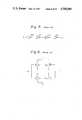
- FIG. 1is a partial circuit diagram of a gate-array LSI having no delay circuit
- FIGS. 2A, 2B, 2C, and 2Dare timing diagrams showing the operation of the circuit of FIG. 1;
- FIG. 3is a partial circuit diagram of a gate-array LSI having a delay circuit
- FIGS. 4A, 4B, 4C, 4D, and 4Eare timing diagrams showing the operation of the circuit of FIG. 3;
- FIG. 5is a circuit diagram of a prior art delay circuit
- FIG. 6is an equivalent circuit diagram of an example of one basic cell used in a complementary MIS gate array LSI;
- FIG. 7is a plan view of the basic cell of FIG. 6;
- FIGS. 8 and 9are cross-sectional views taken along the lines VIII--VIII and IX--IX, respectively, of FIG. 7;
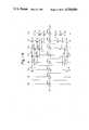
- FIG. 10is a circuit diagram of a first embodiment of the delay circuit according to the present invention.
- FIGS. 11A and 11Bare circuit diagrams for explaining the operation of FIG. 10;
- FIG. 12is circuit diagram of a second embodiment of the delay circuit according to the present invention.
- FIGS. 13 through 16are timing diagrams showing the operation of the circuit of FIG. 12;
- FIG. 17is a circuit diagram of a third embodiment of the delay circuit according to the present invention.
- FIG. 18is a circuit diagram of a fourth embodiment of the delay circuit according to the present invention.
- FIGS. 19 and 20are circuit diagrams for explaining the operation of FIG. 18;
- FIGS. 21 through 24are timing diagrams showing the operation of the circuit of FIG. 18;
- FIG. 25is a circuit diagram of a fifth embodiment of the delay circuit according to the present invention.
- FIG. 26is a circuit diagram of a sixth embodiment of the delay circuit according to the present invention.
- FIGS. 27 and 28are circuit diagrams for explaining the operation of FIG. 26.
- FIG. 1which is a partial circuit diagram of a gate-array LSI
- a clock signal CK 0is delayed by time periods t 1 and t 2 to generate clock signals CK 1 and CK 2 , as shown in FIGS. 2A, 2B, and 2D, thereby latching flip-flops FF1 and FF2.
- the flip-flop FF1is latched by the clock signal CK 1 as shown in FIG. 2C
- a latch operation for the flip-flop FF2 by the clock signal CK 2may be performed upon the next data. This means that the hold time period of the input data of the flip-flop FF2 by the clock signal CK 2 may be reduced.
- a delay circuit DLis interposed between the flip-flops FF 1 and FF 2 , as illustrated in FIG. 3.
- the data output Q of the flip-flop FF1is delayed by a time period t d .
- the data input D of the flip-flop FF2is delayed by the time period t d as compared with the data output Q of the flip-flop FF1, as shown in FIGS. 4C and 4D, and the hold time period of the flip-flop FF2 by the clock signal CK 2 becomes sufficiently large.
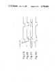
- FIG. 5shows a prior art delay circuit used in a gate-array LSI.
- a series of inverters INVare provided.
- Each of the inverters INVis constructed by a basic cell, which consists, for example, of four two-input gates.
- FIG. 6is an equivalent circuit diagram of a complementary MIS (CMIS) basic cell.
- the basic cellis comprised of a pair of P-channel transistors Q 1p and Q 2p having a common source and a pair of N-channel transistors Q 1n and Q 2n having a common source.
- the gates of the P-channel transistor Q 1p and the N-channel transistor Q 1nare connected to each other, and the gates of the P-channel transistor Q 2p and the N-channel transistor Q 2n are connected to each other.
- FIG. 7which is a plan view of the basic cell of FIG. 6, and FIGS.
- reference numeral 1designates an N - -type monocrystalline silicon substrate 1 having a P - -type well 2 for the N-channel transistors Q 1n and Q 2n . Further, a field oxide layer 3 for isolating transistors (active areas) from each other is formed thereon, and a gate oxide layer 4 is formed on each active area. Further, P + -type impurity diffusion regions 5 are formed for the P-channel transistors Q 1p and Q 2p , and N + -type impurity diffusion regions 5 are formed for the N-channel transistors Q 1n and Q 2n .
- connection patternsare formed on the basic cell as shown in FIGS. 6 through 9.
- each inverter INVis constructed by a basic cell as shown in FIGS. 6 through 9.
- each inverter INVuses only two gates, e.g., the transistors Q 1p and Q 1n , and does not use the other two gates, e.g., the transistors Q 2p and Q 2n .
- the delay time period of the first stageis 0.77 ns
- the delay time period of the second stageis 0.43 ns
- the delay time period of the third stageis 0.77 ns
- the delay time period of the fourth stageis 0.71 ns. Therefore, the total delay time period is 2.68 ns.
- the delay time period of the first stageis 0.43 ns; the delay time period of the second stage is 0.77 ns; the delay time period of the third stage is 0.43 ns; and the delay time of the fourth stage is 1.32 ns. Therefore, the total delay time period is 2.95 ns.
- the delay circuit of FIG. 5requires a large number of inverters stages, i.e., basic cells, occupying a large area.
- FIG. 7which is a first embodiment of the present invention
- P-channel transistors Q 1p , Q 2p , Q 3p and Q 4pare connected in series between a power supply terminal V cc and an output terminal OUT
- N-channel transistors Q 1n , Q 2n , Q 3n , and Q 4nare connected in series between the output terminal OUT and the ground.
- a load capacitance C Lis connected to the output terminal OUT.
- the P-channel transistors Q 1p , Q 2p , Q 3p , and Q 4p and the N-channel transistors Q 1n , Q 2n , Q 3n , and Q 4nare all driven by the potential at the input terminal IN.
- the transistors Q 1p , Q 2p , Q 3p , and Q 4pare in an on state, and the transistors Q 1n , Q 2n , Q 3n , and Q 4n are in an off state. Therefore, the load capacitance C L is changed at V cc by the transistors Q 1p , Q 2p , Q 3p , and Q 4p , so that the potential at the output terminal OUT is high.
- the transistors Q 1n , Q 2n , Q 3n , and Q 4nare in an on state, and the transistors Q 1p , Q 2p , Q 3p , and Q 4p are in an off state. Therefore, the load capacitance C L is discharged by the transistors Q 1n , Q 2n , Q 3n , and Q 4n , so that the potential at the output terminal OUT is low.
- the P-channel transistors Q 1p , Q 2p , Q 3p , and Q 4pare sequentially turned on, in that order, and the N-channel transistors Q 4n , Q 3n , Q 2n , and Q 1n are sequentially turned off, in that order, since the gate-source voltage of a P-channel transistor (N-channel transistor) on the outside is not smaller than the gate-source voltage of a P-channel transistor (N-channel transistor) on the inside.
- the output terminal OUTis charged by the P-channel transistors Q 1p , Q 2p , Q 3p , and Q 4p , so that its potential rises in the same way as the rise operation in a four-input NOR circuit as shown in FIG. 11A.
- the N-channel transistors Q 1n , Q 2n , Q 3n , and Q 4nare sequentially turned on, in that order, and the P-channel transistors Q 4p , Q 3p , Q 2p , and Q 1p are sequentially turned off in that order, since, also in this case, the gate-source voltage of a P-channel transistor (N-channel transistor) on the outside is not smaller than the gate-source voltage of a P-channel transistor (N-channel transistor) on the inside.
- the output terminal OUTis discharged by the N-channel transistors Q 1n , Q 2n , Q 3n , and Q 4n , so that its potential falls in the same way as the fall operation in a four-input NAND circuit as shown in FIG. 11B.
- the P-channel transistors(or the N-channel transistors) are sequentially turned on from the outside to the inside, and the N-channel transistors (or the P-channel transistors) are turned on, the change of the potential at the output terminal OUT is delayed.
- FIG. 12which is a circuit diagram of a second embodiment of the delay circuit according to the present invention
- an inverter INVAis comprised of P-channel transistors Q 1p , Q 2p , Q 3p , and Q 4p and N-channel transistors Q 1n , Q 2n , Q 3n , and Q 4n connected in series
- an inverter INVBis comprised of P-channel transistors Q 1p ', Q 2p ', Q 3p ', and Q 4p ' and N-channel transistors Q 1 ', Q 2 ', Q 3 ', and Q 4 ' connected in series.
- the potential at the input terminal INis applied to the gates of the transistors Q 1p , Q 2p , Q 3p , Q 4p , Q 1n , Q 2n , Q 3n , and Q 4n of the inverter INVA. Accordingly, these transistors are driven by the potential at the input terminal IN. Also, the common output C of the innermost pair of the P-channel/N-channel transistors Q 4p and Q 4n of the inverter INVA is applied to the gates of the transistors Q 1p ', Q 2p ', Q 3p ',Q 4p ', Q 1N ', Q 2n ', Q 3n ', and Q 4n 'of the inverter INVB.
- these transistorsare driven by the potential at the output C. Also, the common output of the innermost pair of the P-channel/N-channel transistors Q 4p ' and Q 4n ' of the inverter INVB is connected to the output terminal OUT.
- the transistors Q 1p , Q 2p , Q 1n , and Q 2ncan be constructed by one basic cell; the transistors Q 3p , Q 4p , Q 3n , and Q 4n can be constructed by one basic cell; the transistors Q 1p ', Q 2p ', Q 1n ', and Q 2n ' can be constructed by one basic cell; and the transistors Q 3p ', Q 4p ', Q 3n ', and Q 4n ' can be constructed by one basic cell. Therefore, the circuit of FIG. 12 can be constructed by four basic cells in the same way as in the circuit of FIG. 5.
- FIGS. 13 through 16The operation of the circuit of FIG. 12 is shown in FIGS. 13 through 16.
- FIG. 13shows the case wherein the fan-out (F/O) is 0 and wherein the potential at the input terminal IN is changed from low to high
- FIG. 14shows the case wherein the fan-out (F/O) is 0 and wherein the potential at the input terminal IN is changed from high to low
- FIG. 15shows the case wherein the fan-out (F/O) is 5 and wherein the potential at the input terminal IN is changed from low to high
- FIG. 16shows the case wherein the fan-out (F/O) is 5 and wherein the potential at the input terminal IN is changed from high to low.
- the P-channel transistors Q 1p , Q 2p , Q 3p , and Q 4pare in an on state, and the N-channel transistors Q 1n , Q 2n , Q 3n , and Q 4n are in an off state, and, accordingly, the potential at the node C is high. Therefore, in the inverter INVB, P-channel transistors Q 1p , Q 2p , Q 3p , and Q 4p are in an off state, and the N-channel transistors Q 1n , Q 2n , Q 3n , and Q 4n are in an on state, and accordingly, the potential at the output terminal OUT is low.
- the transistors Q 1n , Q 2n , Q 3n , and Q 4nbecome in an on state, the node C is discharged via these transistors. As a result, the potential at the node C is reduced, and simultaneously, the potentials at the nodes B 1 , B 2 , and B 3 change toward their DC stable points determined by the impedance ratio of the transistors.
- the transistors Q 1p ', Q 2p ', Q 3p ', and Q 4p 'tend to be in an on state, and accordingly, the potentials at the nodes D 1 , D 2 , and D 3 change toward a DC stable point determined by the impedance ratio of the transistors Q 1p ', Q 2p ', Q 3p ', and Q 4p '.
- the potentials at the nodes E 1 , E 2 , and E 3become lower than the ground level due to the rapid reduction of the potential at the node C.
- the transistors Q 1n , Q 2n , Q 3n , and Q 4nare completely in an on state. Therefore, the potentials at the nodes C, B 1 , B 2 , and B 3 are reduced by the discharging operation. Note that, at this time, since the transistors Q 1p , Q 2p , Q 3p , and Q 4p are completely in an off state, the potentials at the nodes E 1 , E 2 , and E 3 become levels in accordance with the impedance determined by the leakage currents of the transistors Q 1n ', Q 2n ', Q 3n ', and Q 4n ' after a sufficient time period passes.
- the potential at the output terminal OUTis changed by the discharging operation of the transistors Q 1p ', Q 2p ', Q 3p ', and Q 4p ', and the transistors Q 1n , Q 2n , Q 3n , and Q 4n .
- a charging and discharging operationis carried out by a large number of transistors, thereby increasing the delay time period.
- FIG. 13is replaced by FIG. 15, and FIG. 14 is replaced by FIG. 16. That is, the waveform at the output terminal OUT is blunt and the delay time period is further increased.
- a delay time period having a time larger than 5 nscan be obtained, and therefore, is larger than that of FIG. 5.
- each of the invertershas the same number of P-channel transistors and N-channel transistors connected in series. Any number can be, of course, selected, however.
- FIG. 17which illustrates a third embodiment of the present invention
- two inverters INVA' and INVB'are added to the circuit of FIG. 12. That is, the inverter INVA' is interposed between the inverters INVA and INVB, and the inverter INVB' is connected to the output of the inverter INVB.
- the inverters INVA' and INVB'serve as wave-shaping means. Each of them is constructed by two gates of one basic cell, as shown in FIGS. 6 through 9.
- FIG. 18which illustrates a fourth embodiment of the present invention, two inverters INVA and INVB are also provided.
- each pair of P-channel/N-channel transistors Q 1p and Q 1n ; Q 2p and Q 2n ; Q 3p and Q 3n ; and Q 4p and Q 4nform one inverter.
- each pair of P-channel/N-channel transistors Q 1p ' and Q 1n '; Q 2p ' and Q 2n '; Q 3p ' and Q 3n '; and Q 4p ' and Q 4n 'forms one inverter.
- the circuit of FIG. 18would be as schematically illustrated in FIG. 19.
- the P-channel transistors Q p and N-channel transistors Q n of FIG. 19are absent in FIG. 18. They are provided in FIG. 19 only for easy understanding of the operation thereof.
- the inverters INV 3 to INV 8were defined by transfer gates, the circuit of FIG. 18 would be as schematically illustrated in FIG. 20.
- the inverter INV 1(Q 1p , Q 1n ) is driven by the potential at the input terminal IN; the inverter INV 2 (Q 1p ', Q 1n ') is driven by the output A of the inver INV 1 ; the inverter INV 3 (Q 2p , Q 2n ) is driven by the output B of the inverter INV 2 ; the inverter INV 4 (Q 2p ', Q 2n ') is driven by the output C of the inverter the inverter INV 3 ; the inverter INV 5 (Q 3p , Q 3n ) is driven by the output D of the inverter INV 4 ; the inverter INV 6 (Q 3p ', Q 3n ') is driven by the output E of the inverter INV 5 ; the inverter INV 7 (Q 4p , Q 4n ) is driven by the output F of the inverter INV 6 ; the inverter INV
- each inverter of the post-stage inverter INVBis fed back to the input of each inverter of the pre-stage inverter INVA. Accordingly, the driving power of each inverter (INV 1 to INV 8 ) is reduced, thereby increasing the delay time period.
- circuit of FIG. 18is constructed by basic cells each having four two-input gates as shown in FIGS. 6 through 9, the circuit of FIG. 18 can be constructed by four basic cells in the same way as in the circuit of FIG. 12.
- FIGS. 21 through 24The operation of the circuit of FIG. 18 is shown in FIGS. 21 through 24.
- FIGS. 21 through 24correspond to FIGS. 13 through 16, respectively. That is, FIG. 21 shows the case wherein the fan-out (F/O) is 0 and wherein the potential at the input terminal IN is changed from low to high; FIG. 22 shows the case wherein the fan-out (F/O) is 0 and wherein the potential at the input terminal IN is changed from high to low; FIG. 23 shows the case wherein the fan-out (F/O) is 5 and wherein the potential at the input terminal IN is changed from low to high; and FIG. 24 shows the case wherein the fan-out (F/O) is 5 and wherein the potential at the input terminal IN is changed from high to low.
- the transistor Q 2pWhen the potential at the output B reaches the above-mentioned threshold value, the transistor Q 2p is cut off, and the discharge at the outputs C, E, and G temporarily ceases. Further, when the potential at the output B increases, the potential at the output C remains temporarily at the same level and, accordingly, the transistor Q 2n ' is cut off. As a result, only the potential at the output B increases. Therefore, the output C of the inverter INV 3 (Q 2p , Q 2n ) is again reduced. At this time, since the transistors Q 3p and Q 4p are still in an on state, the potentials at the outputs E and G are also reduced.
- FIG. 21is replaced by FIG. 23 and FIG. 22 is replaced by FIG. 24. That is, the waveform at the output terminal OUT is blunt and the delay time period is further increased.
- a delay time period having a time larger than 5 nscan be obtained and therefore, is larger than that of FIG. 5.
- FIG. 25which illustrates a fifth embodiment of the present invention similar to the fourth embodiment as shown in FIG. 18, the inverters INV 3 (Q 2p , Q 2n ), INV 5 (Q 3p , Q 3n ), and INV 7 (Q 4p , Q 4n ) of the inverter INVA are driven simultaneously by the output B of the inverter INV 2 (Q 1p ', Q 1n ') of the inverter INVB, and the inverters INV 4 (Q 2p ', Q 2n '), INV 6 (Q 3p ', Q 3n '), and INV 8 (Q 4p ', Q 4n ') of the inverter INVB are driven simultaneously by the output of the inverter INV 7 (Q 4p , Q 4n ) of the inverter INVA.
- the P-channel transistors Q 2p , Q 3p , and Q 4p and the N-channel transistors Q 2n , Q 3n , and Q 4ntend to be in an on state, and accordingly, the high potential at the output A is transmitted to the output C. Therefore, the output C becomes high, so that the potential at the output terminal OUT becomes low. In such a configuration, unstable waveforms are hardly over generated in the output terminal OUT as compared with the embodiment of FIG. 18.
- FIG. 26which illustrates a sixth embodiment of the present invention similar to the embodiment of FIG. 25, the inverters INV 3 (Q 2p , Q 2n ), INV 5 (Q 3p , Q 3n ), and INV 7 (Q 4p , Q 4n ) of the inverter INVA are driven by the potential at the output terminal OUT, not the output of the inverter INV 2 (Q 1p ', Q 1n ') of the inverter INVB.
- the transistors Q 2p , Q 3p , and Q 4pare still in an on state, the potentials at the nodes C 1 and C 2 and at the node B are also decreased with the decrease of the potential A.
- the transistors Q 4p ', Q 3p ', and Q 2p 'tend to be in an on state, so that the nodes E 1 , E 2 , and E 3 are discharged to decrease the potentials thereof. Instead, the potentials at the output terminal OUT and the nodes F 1 , F 2 , and F 3 are increased.
- Such an unstable statecontinues until the potential at the output terminal OUT reaches the threshold value of the P-channel transistor Q 2p . When the potential at the output terminal OUT reaches this threshold value, the transistors Q 2p , Q 3p , and Q 4p are cut off to again decrease the potential at the node B.
- the transistors Q 2n , Q 3n , and Q 4nare still in an on state, the potentials at the nodes D 1 and D 2 and at the node B are also increased with the increase of the potential A.
- the transistors Q 4n' , Q 3n' , and Q 2n 'tend to be in an on state, so that the nodes F 1 , F 2 , and F 3 are charged to increase the potentials thereof.
- the potentials at the output terminal OUT and the nodes E 1 , E 2 , and E 3are reduced.
- Such an unstable statecontinues until the potential at the output terminal OUT reaches the threshold value of the N-channel transistor Q 4n .
- the transistors Q 2n , Q 3n , and Q 4nare cut off to again increase the potential at node B.
- the delay time periodis larger than 17 ns, while when the potential at the input terminal IN is changed from high to low, the delay time is larger than 7 ns. In any case, a delay time period having a time larger than 5 ns can be obtained and therefore, is larger than that of FIG. 5.
- FIGS. 27 and 28show the case where the fan-out is 0. However, if the fan-out is larger than 1, the delay time period is further increased.
- the delay time periodcan be increased as compared with the prior art where a plurality of inverters are simply connected in series. In other words, with the same delay time period, it is possible to reduce the area occupied by the delay circuit.
Landscapes
- Physics & Mathematics (AREA)
- Nonlinear Science (AREA)
- Logic Circuits (AREA)
- Pulse Circuits (AREA)
Abstract
Description
1. Field of the Invention
The present invention relates to a delay circuit applied to, for example, a gate-array large-scale integrated circuit (LSI).
2. Description of the Related Art
In a gate-array LSI, a delay circuit is used for delaying the propagation of a signal for a definite time period. Such a delay circuit must offer an optimum delay time period, a small mounting area, and minimum fluctuation of the delay time period.
In general, a delay time period tpd of one gate of a metal-insulator-semiconductor (MIS) transistor can be represented by
t.sub.pd αC/g.sub.m
where C is a load, capacitance, and gm is the conductance of the transistor. Further, if the load capacitance is definite,
g.sub.m αW/L
where W and L are the width and length, respectively, of a gate of the transistor. Therefore, it is possible to increase the delay time period by using an inverter of MIS transistors having a small gate width W and a large gate length L. However, in a gate-array LSI, since only transistors having a definite size are used, it is impossible to arbitrarily change the size of the transistors. In other words, in a gate-array LSI, it is impossible to decrease the gate width W and increase the gate length L only for special transistors.
There is a prior art delay circuit of a gate-array LSI comprised of a series of inverters of MIS transistors having a definite size. However, when a series of such inverters are simply connected to obtain a delay time period, the larger the delay time period, the greater the number of transistors, and thus the larger the area occupied.
Note that it is also possible to construct a delay circuit by using a resistance-capacitance (RC) circuit. In this case, the delay time period must be adjusted by the resistance of polycrystalline silicon or the resistance of a diffusion region. However, such an adjustment is also impossible in a gate-array LSI. Accordingly, it is impossible to use an RC circuit as a delay circuit for a gate-array LSI.
It is an object of the present invention to provide a delay circuit, suitable for a gate-array LSI, having a small area.
According to the present invention, the delay circuit includes at least one inverter having a plurality of P-channel transistors and a plurality of N-channel transistors connected in series. In this case, the P-channel transistors are sequentially turned on from the outside to the inside by the fall of an input potential, while the P-channel transistors are sequentially turned off from the inside to the outside by the rise of the input potential. Similarly, the N-channel transistors are sequentially turned on from the outside to the inside by the rise of the input potential, while the N-channel transistors are sequentially turned off from the inside to the outside by the fall of the input potential.
Also in the present invention, two inverters having series-connected P-channel/N-channel transistors are provided. In this case, the output of each inverter is charged by the series-connected P-channel transistors thereof to increase the potential of this output, while the output of each inverter is discharged by the series connected N-channel transistors thereof to decrease the potential of this output. Therefore, the delay time period is increased by the P-channel/N-channel transistors in series.
Further, in the present invention, two inverters having series-connected P-channel/N-channel transistors, in which the outputs of the post-stage inverter are fed back to some of the inputs of the pre-stage inverters, are provided. In this case, since the outputs of the post-stage inverter are fed back to the pre-stage inverter, the driving ability thereof is reduced, thereby increasing the delay time period. Also, a large fan-out is obtained.
The present invention will be more clearly understood from the description as set forth below, with reference to the accompanying drawings, wherein:
FIG. 1 is a partial circuit diagram of a gate-array LSI having no delay circuit;
FIGS. 2A, 2B, 2C, and 2D are timing diagrams showing the operation of the circuit of FIG. 1;
FIG. 3 is a partial circuit diagram of a gate-array LSI having a delay circuit;
FIGS. 4A, 4B, 4C, 4D, and 4E are timing diagrams showing the operation of the circuit of FIG. 3;
FIG. 5 is a circuit diagram of a prior art delay circuit;
FIG. 6 is an equivalent circuit diagram of an example of one basic cell used in a complementary MIS gate array LSI;
FIG. 7 is a plan view of the basic cell of FIG. 6;
FIGS. 8 and 9 are cross-sectional views taken along the lines VIII--VIII and IX--IX, respectively, of FIG. 7;
FIG. 10 is a circuit diagram of a first embodiment of the delay circuit according to the present invention;
FIGS. 11A and 11B are circuit diagrams for explaining the operation of FIG. 10;
FIG. 12 is circuit diagram of a second embodiment of the delay circuit according to the present invention;
FIGS. 13 through 16 are timing diagrams showing the operation of the circuit of FIG. 12;
FIG. 17 is a circuit diagram of a third embodiment of the delay circuit according to the present invention;
FIG. 18, is a circuit diagram of a fourth embodiment of the delay circuit according to the present invention;
FIGS. 19 and 20 are circuit diagrams for explaining the operation of FIG. 18;
FIGS. 21 through 24 are timing diagrams showing the operation of the circuit of FIG. 18;
FIG. 25 is a circuit diagram of a fifth embodiment of the delay circuit according to the present invention;
FIG. 26 is a circuit diagram of a sixth embodiment of the delay circuit according to the present invention; and
FIGS. 27 and 28 are circuit diagrams for explaining the operation of FIG. 26.
In FIG. 1, which is a partial circuit diagram of a gate-array LSI, it is assumed that a clock signal CK0 is delayed by time periods t1 and t2 to generate clock signals CK1 and CK2, as shown in FIGS. 2A, 2B, and 2D, thereby latching flip-flops FF1 and FF2. In this case, after the flip-flop FF1 is latched by the clock signal CK1 as shown in FIG. 2C, if the delay time period t2 of the clock signal CK2 is large, a latch operation for the flip-flop FF2 by the clock signal CK2 may be performed upon the next data. This means that the hold time period of the input data of the flip-flop FF2 by the clock signal CK2 may be reduced.
In order to secure a sufficient hold time period, a delay circuit DL is interposed between the flip-flops FF1 and FF2, as illustrated in FIG. 3. As a result, the data output Q of the flip-flop FF1 is delayed by a time period td. Thus, the data input D of the flip-flop FF2 is delayed by the time period td as compared with the data output Q of the flip-flop FF1, as shown in FIGS. 4C and 4D, and the hold time period of the flip-flop FF2 by the clock signal CK2 becomes sufficiently large.
FIG. 5 shows a prior art delay circuit used in a gate-array LSI. A series of inverters INV are provided. Each of the inverters INV is constructed by a basic cell, which consists, for example, of four two-input gates.
An example of a basic cell will now be explained with reference to FIGS. 6, 7, 8, and 9.
FIG. 6 is an equivalent circuit diagram of a complementary MIS (CMIS) basic cell. The basic cell is comprised of a pair of P-channel transistors Q1p and Q2p having a common source and a pair of N-channel transistors Q1n and Q2n having a common source. In this case, the gates of the P-channel transistor Q1p and the N-channel transistor Q1n are connected to each other, and the gates of the P-channel transistor Q2p and the N-channel transistor Q2n are connected to each other. Referring to FIG. 7, which is a plan view of the basic cell of FIG. 6, and FIGS. 8 and 9, which are cross-sectional views,reference numeral 1 designates an N- -typemonocrystalline silicon substrate 1 having a P- -type well 2 for the N-channel transistors Q1n and Q2n. Further, afield oxide layer 3 for isolating transistors (active areas) from each other is formed thereon, and agate oxide layer 4 is formed on each active area. Further, P+ -typeimpurity diffusion regions 5 are formed for the P-channel transistors Q1p and Q2p, and N+ -typeimpurity diffusion regions 5 are formed for the N-channel transistors Q1n and Q2n. Finally, polycrystalline silicon layers 7 are formed for the connection of the gates of the transistors Q1p and Q1n and the connection of the gates of the transistors Q2p and Q2n, thus completing the bulk process of a gate-array LSI. After that, as occasion demands, that is, as customers demand, connection patterns are formed on the basic cell as shown in FIGS. 6 through 9.
Returning to FIG. 5, as stated above, each inverter INV is constructed by a basic cell as shown in FIGS. 6 through 9. In this case, each inverter INV uses only two gates, e.g., the transistors Q1p and Q1n, and does not use the other two gates, e.g., the transistors Q2p and Q2n. In FIG. 5, when the potential at the input terminal IN is changed from high to low, the delay time period of the first stage is 0.77 ns; the delay time period of the second stage is 0.43 ns; the delay time period of the third stage is 0.77 ns; and the delay time period of the fourth stage is 0.71 ns. Therefore, the total delay time period is 2.68 ns. On the contrary, when the potential at the input terminal IN is changed from low to high, the delay time period of the first stage is 0.43 ns; the delay time period of the second stage is 0.77 ns; the delay time period of the third stage is 0.43 ns; and the delay time of the fourth stage is 1.32 ns. Therefore, the total delay time period is 2.95 ns.
In order to obtain a large delay time period, the delay circuit of FIG. 5 requires a large number of inverters stages, i.e., basic cells, occupying a large area.
In FIG. 7, which is a first embodiment of the present invention, P-channel transistors Q1p, Q2p, Q3p and Q4p are connected in series between a power supply terminal Vcc and an output terminal OUT, and N-channel transistors Q1n, Q2n, Q3n, and Q4n are connected in series between the output terminal OUT and the ground. Further, a load capacitance CL is connected to the output terminal OUT. The P-channel transistors Q1p, Q2p, Q3p, and Q4p and the N-channel transistors Q1n, Q2n, Q3n, and Q4n are all driven by the potential at the input terminal IN. For example, when the potential at the input terminal IN is low, the transistors Q1p, Q2p, Q3p, and Q4p are in an on state, and the transistors Q1n, Q2n, Q3n, and Q4n are in an off state. Therefore, the load capacitance CL is changed at Vcc by the transistors Q1p, Q2p, Q3p, and Q4p, so that the potential at the output terminal OUT is high. On the other hand, when the potential at the input terminal IN is high, the transistors Q1n, Q2n, Q3n, and Q4n are in an on state, and the transistors Q1p, Q2p, Q3p, and Q4p are in an off state. Therefore, the load capacitance CL is discharged by the transistors Q1n, Q2n, Q3n, and Q4n, so that the potential at the output terminal OUT is low.
Therefore, when the potential at the input terminal IN is changed from high to low, the P-channel transistors Q1p, Q2p, Q3p, and Q4p are sequentially turned on, in that order, and the N-channel transistors Q4n, Q3n, Q2n, and Q1n are sequentially turned off, in that order, since the gate-source voltage of a P-channel transistor (N-channel transistor) on the outside is not smaller than the gate-source voltage of a P-channel transistor (N-channel transistor) on the inside. As a result, the output terminal OUT is charged by the P-channel transistors Q1p, Q2p, Q3p, and Q4p , so that its potential rises in the same way as the rise operation in a four-input NOR circuit as shown in FIG. 11A.
On the other hand, when the potential at the input terminal IN is changed from low to high, the N-channel transistors Q1n, Q2n, Q3n, and Q4n are sequentially turned on, in that order, and the P-channel transistors Q4p, Q3p, Q2p, and Q1p are sequentially turned off in that order, since, also in this case, the gate-source voltage of a P-channel transistor (N-channel transistor) on the outside is not smaller than the gate-source voltage of a P-channel transistor (N-channel transistor) on the inside. As a result, the output terminal OUT is discharged by the N-channel transistors Q1n, Q2n, Q3n, and Q4n, so that its potential falls in the same way as the fall operation in a four-input NAND circuit as shown in FIG. 11B.
Thus, since the P-channel transistors (or the N-channel transistors) are sequentially turned on from the outside to the inside, and the N-channel transistors (or the P-channel transistors) are turned on, the change of the potential at the output terminal OUT is delayed.
Note that the fluctuation in the operation of the circuit of FIG. 10 is about the same as in conventional logic circuits.
In FIG. 12, which is a circuit diagram of a second embodiment of the delay circuit according to the present invention, two inverters as shown in FIG. 10 are provided. That is, an inverter INVA is comprised of P-channel transistors Q1p, Q2p, Q3p, and Q4p and N-channel transistors Q1n, Q2n, Q3n, and Q4n connected in series, and an inverter INVB is comprised of P-channel transistors Q1p ', Q2p ', Q3p ', and Q4p ' and N-channel transistors Q1 ', Q2 ', Q3 ', and Q4 ' connected in series.
In FIG. 12, the potential at the input terminal IN is applied to the gates of the transistors Q1p, Q2p, Q3p, Q4p, Q1n, Q2n, Q3n, and Q4n of the inverter INVA. Accordingly, these transistors are driven by the potential at the input terminal IN. Also, the common output C of the innermost pair of the P-channel/N-channel transistors Q4p and Q4n of the inverter INVA is applied to the gates of the transistors Q1p ', Q2p ', Q3p ',Q4p ', Q1N ', Q2n ', Q3n ', and Q4n 'of the inverter INVB. Accordingly, these transistors are driven by the potential at the output C. Also, the common output of the innermost pair of the P-channel/N-channel transistors Q4p ' and Q4n ' of the inverter INVB is connected to the output terminal OUT.
Note that, if the circuit of FIG. 12 is constructed by basic cells each having four two-input gates, as shown in FIGS. 6 through 9, the transistors Q1p, Q2p, Q1n, and Q2n can be constructed by one basic cell; the transistors Q3p, Q4p , Q3n, and Q4n can be constructed by one basic cell; the transistors Q1p ', Q2p ', Q1n ', and Q2n ' can be constructed by one basic cell; and the transistors Q3p ', Q4p ', Q3n ', and Q4n ' can be constructed by one basic cell. Therefore, the circuit of FIG. 12 can be constructed by four basic cells in the same way as in the circuit of FIG. 5.
The operation of the circuit of FIG. 12 is shown in FIGS. 13 through 16. FIG. 13 shows the case wherein the fan-out (F/O) is 0 and wherein the potential at the input terminal IN is changed from low to high; FIG. 14 shows the case wherein the fan-out (F/O) is 0 and wherein the potential at the input terminal IN is changed from high to low; FIG. 15 shows the case wherein the fan-out (F/O) is 5 and wherein the potential at the input terminal IN is changed from low to high; and FIG. 16 shows the case wherein the fan-out (F/O) is 5 and wherein the potential at the input terminal IN is changed from high to low.
Referring to FIG. 13, first, if the potential at the input terminal IN is low, the P-channel transistors Q1p, Q2p, Q3p, and Q4p are in an on state, and the N-channel transistors Q1n, Q2n, Q3n, and Q4n are in an off state, and, accordingly, the potential at the node C is high. Therefore, in the inverter INVB, P-channel transistors Q1p, Q2p, Q3p, and Q4p are in an off state, and the N-channel transistors Q1n, Q2n, Q3n, and Q4n are in an on state, and accordingly, the potential at the output terminal OUT is low. In this state, when the potential at the input terminal IN is changed from low to high, the N-channel transistors Q1n, Q2n, Q3n, and Q4n tend to be in an on state, while the transistors Q1p, Q2p, Q3p, and Q4p tend to be in an off state. At this time, when the change of the potential at the input terminal IN is rather rapid, the potentials at the nodes A1, A2, A3, and C temporarily rise up to a level higher than the power supply potential Vcc by the gate-source capacitance of each of the transistors Q1p to Q4p and Qrn. Then, as the transistors Q1n, Q2n, Q3n, and Q4n become in an on state, the node C is discharged via these transistors. As a result, the potential at the node C is reduced, and simultaneously, the potentials at the nodes B1, B2, and B3 change toward their DC stable points determined by the impedance ratio of the transistors. In addition, as the potential at the node C is reduced, the transistors Q1p ', Q2p ', Q3p ', and Q4p ' tend to be in an on state, and accordingly, the potentials at the nodes D1, D2, and D3 change toward a DC stable point determined by the impedance ratio of the transistors Q1p ', Q2p ', Q3p ', and Q4p '. At this time, the potentials at the nodes E1, E2, and E3 become lower than the ground level due to the rapid reduction of the potential at the node C.
Next, when the potential at the input terminal IN becomes a sufficiently high level, the transistors Q1n, Q2n, Q3n, and Q4n are completely in an on state. Therefore, the potentials at the nodes C, B1, B2, and B3 are reduced by the discharging operation. Note that, at this time, since the transistors Q1p, Q2p, Q3p, and Q4p are completely in an off state, the potentials at the nodes E1, E2, and E3 become levels in accordance with the impedance determined by the leakage currents of the transistors Q1n ', Q2n ', Q3n ', and Q4n ' after a sufficient time period passes.
Thus, the potential at the output terminal OUT is changed by the discharging operation of the transistors Q1p ', Q2p ', Q3p ', and Q4p ', and the transistors Q1n, Q2n , Q3n, and Q4n. However, in this case, a charging and discharging operation is carried out by a large number of transistors, thereby increasing the delay time period.
In addition, when the potential at the input terminal IN is changed from high to low, the potential at each node is changed as shown in FIG. 14. A detailed explanation is omitted, since it is similar to that of FIG. 13, however, in this case, the potential at the output terminal OUT is changed by the discharging operation of the transistors Q1p, Q2p, Q3p, and Q4p and and the transistors Q1n ', Q2n ', Q3n ', and Q4n '.
Note that, in the case wherein the fan-out is 5, FIG. 13 is replaced by FIG. 15, and FIG. 14 is replaced by FIG. 16. That is, the waveform at the output terminal OUT is blunt and the delay time period is further increased.
In any case, a delay time period having a time larger than 5 ns can be obtained, and therefore, is larger than that of FIG. 5.
Note that, in the above-mentioned embodiments of FIGS. 10 and 12, each of the inverters has the same number of P-channel transistors and N-channel transistors connected in series. Any number can be, of course, selected, however.
In FIG. 17, which illustrates a third embodiment of the present invention, two inverters INVA' and INVB' are added to the circuit of FIG. 12. That is, the inverter INVA' is interposed between the inverters INVA and INVB, and the inverter INVB' is connected to the output of the inverter INVB. The inverters INVA' and INVB' serve as wave-shaping means. Each of them is constructed by two gates of one basic cell, as shown in FIGS. 6 through 9.
In FIG. 18, which illustrates a fourth embodiment of the present invention, two inverters INVA and INVB are also provided. In the inverter INVA, each pair of P-channel/N-channel transistors Q1p and Q1n ; Q2p and Q2n ; Q3p and Q3n ; and Q4p and Q4n form one inverter. Similarly, in the inverter INVB, each pair of P-channel/N-channel transistors Q1p ' and Q1n '; Q2p ' and Q2n '; Q3p ' and Q3n '; and Q4p ' and Q4n ' forms one inverter.
Here, if the pairs of the transistors Q1p and Q1n ; Q1p ' and Q1n '; Q2p and Q2n ; Q2p ' and Q2n '; Q3p and Q3n ; Q3p ' and Q3n '; Q4p and Q4n ; and Q4p ' and Q4n ' were defined by inverters INV1, INV2, INV3, INV4, INV5, INV6, INV7, and INV8, respectively, the circuit of FIG. 18 would be as schematically illustrated in FIG. 19. Note that the P-channel transistors Qp and N-channel transistors Qn of FIG. 19 are absent in FIG. 18. They are provided in FIG. 19 only for easy understanding of the operation thereof. Further, if the inverters INV3 to INV8 were defined by transfer gates, the circuit of FIG. 18 would be as schematically illustrated in FIG. 20.
That is, in FIG. 18, the inverter INV1 (Q1p, Q1n) is driven by the potential at the input terminal IN; the inverter INV2 (Q1p ', Q1n ') is driven by the output A of the inver INV1 ; the inverter INV3 (Q2p, Q2n) is driven by the output B of the inverter INV2 ; the inverter INV4 (Q2p ', Q2n ') is driven by the output C of the inverter the inverter INV3 ; the inverter INV5 (Q3p, Q3n) is driven by the output D of the inverter INV4 ; the inverter INV6 (Q3p ', Q3n ') is driven by the output E of the inverter INV5 ; the inverter INV7 (Q4p, Q4n) is driven by the output F of the inverter INV6 ; the inverter INV8 (Q4p ', Q4n ') is driven by the output G of the inverter INV8 ; and the output of the inverter INV8 becomes the potential at the output terminal OUT.
Thus, the output of each inverter of the post-stage inverter INVB is fed back to the input of each inverter of the pre-stage inverter INVA. Accordingly, the driving power of each inverter (INV1 to INV8) is reduced, thereby increasing the delay time period.
Note that, if the circuit of FIG. 18 is constructed by basic cells each having four two-input gates as shown in FIGS. 6 through 9, the circuit of FIG. 18 can be constructed by four basic cells in the same way as in the circuit of FIG. 12.
The operation of the circuit of FIG. 18 is shown in FIGS. 21 through 24.
FIGS. 21 through 24 correspond to FIGS. 13 through 16, respectively. That is, FIG. 21 shows the case wherein the fan-out (F/O) is 0 and wherein the potential at the input terminal IN is changed from low to high; FIG. 22 shows the case wherein the fan-out (F/O) is 0 and wherein the potential at the input terminal IN is changed from high to low; FIG. 23 shows the case wherein the fan-out (F/O) is 5 and wherein the potential at the input terminal IN is changed from low to high; and FIG. 24 shows the case wherein the fan-out (F/O) is 5 and wherein the potential at the input terminal IN is changed from high to low.
Referring to FIG. 21, it is assumed that the potentials at the input terminal IN, the outputs B, D, F, and the output terminal OUT are low, and the potentials at the outputs A, C, E, and G are high. At this time, when the potential at the input terminal IN is changed from low to high, the transistor Q1p is turned off and the transistor Q1n is turned on. As a result, the potential at the output A of the inverter INV1 (Q1p, Q1n) is reduced. At this time, since the transistors Q2p, Q3p, and Q4p are still in an on state, the potentials at the outputs C, E, and G are also reduced. Such a potential reduction continues until the output B of the inverter INV2, (Q1p ', Q1n ') reaches the threshold value of the P-channel transistor Q2p. On the other hand, as the potential at the output A is reduced, the potential at the output B of the inverter INV2 (Q1p ', Q1n ') rises. However, in this case, since the the transistors Q2n ', Q3n ', and Q4n ' are still in an on state, the potentials at the output D, F, and the output terminal OUT are increased simultaneously with the rise of the potential of the output B. When the potential at the output B reaches the above-mentioned threshold value, the transistor Q2p is cut off, and the discharge at the outputs C, E, and G temporarily ceases. Further, when the potential at the output B increases, the potential at the output C remains temporarily at the same level and, accordingly, the transistor Q2n ' is cut off. As a result, only the potential at the output B increases. Therefore, the output C of the inverter INV3 (Q2p, Q2n) is again reduced. At this time, since the transistors Q3p and Q4p are still in an on state, the potentials at the outputs E and G are also reduced. Such a potential reduction continues until the output D of the inverter INV4 (Q2p ', Q2n ') reaches the threshold value of the P-channel transistor Q3p. When the potential at the output D reaches this threshold value, the transistor Q3p is cut off, and the discharge at the outputs E and G temporarily ceases. Further, when the potential at the output D increases, the potential at the output E remains temporarily at the same level, and accordingly, the transistor Q3n ' is cut off. As a result, only the potential at the output E increases. At this time, since the transistor Q4p is still in an on state, the potential at the output G is also reduced. Such a potential reduction continues until the output F of the inverter INV6 (Q3p ', Q3n ') reaches the threshold value of the P-channel transistor Q4p. When the potential at the output F reaches this threshold value, the transistor Q4p is cut off, and the discharge at the output G temporarily ceases. Further, when the potential at the output F increases, the potential at the output G remains temporarily at the same level. Accordingly, the transistor Q4n ' is cut off. As a result, only the potential at the output F increases. Therefore, the output G of the inverter INV7 (Q4p, Q4n) is again reduced, so that the potential at the output terminal OUT rises.
Contrary to the above, in a state where the potentials at the input terminal IN, the outputs B, D, F, and the output terminal OUT are high and the potentials at the outputs A, C, E, and G are low, when the potential at the input terminal IN is changed from high to low, the potential at each node is changed as shown in FIG. 22. A detailed explanation thereof is omitted, since it is similar to that of FIG. 21.
Thus, since saddle points are generated in the change of the potentials at the outputs C, E, and G and at the outputs B, D, and F, the delay time period is increased.
Note that, in the case wherein the fan-out is 5, FIG. 21 is replaced by FIG. 23 and FIG. 22 is replaced by FIG. 24. That is, the waveform at the output terminal OUT is blunt and the delay time period is further increased.
In any case, a delay time period having a time larger than 5 ns can be obtained and therefore, is larger than that of FIG. 5.
In FIG. 25, which illustrates a fifth embodiment of the present invention similar to the fourth embodiment as shown in FIG. 18, the inverters INV3 (Q2p, Q2n), INV5 (Q3p, Q3n), and INV7 (Q4p, Q4n) of the inverter INVA are driven simultaneously by the output B of the inverter INV2 (Q1p ', Q1n ') of the inverter INVB, and the inverters INV4 (Q2p ', Q2n '), INV6 (Q3p ', Q3n '), and INV8 (Q4p ', Q4n ') of the inverter INVB are driven simultaneously by the output of the inverter INV7 (Q4p, Q4n) of the inverter INVA. In this circuit of FIG. 25, in a state where the potentials at the input terminal IN and the output B are high, and the potentials at the outputs A and C are low, when the potential at the input terminal IN is changed from high to low, the output A is changed from low to high. At this time, since the potential at the output C is low, the P-channel transistors Q2p ', Q3p ', and Q4p ' are in an on state, while, since the potential at the output A is high, the N-channel transistor Q1n ' is in an on state. Therefore, the potential at the output B changes toward the PC stable point determined by the impedance ratio of the transistors Q2p ', Q3p ', and Q4p ' to the transistor Q1n '. As a result, the P-channel transistors Q2p, Q3p, and Q4p and the N-channel transistors Q2n, Q3n, and Q4n tend to be in an on state, and accordingly, the high potential at the output A is transmitted to the output C. Therefore, the output C becomes high, so that the potential at the output terminal OUT becomes low. In such a configuration, unstable waveforms are hardly over generated in the output terminal OUT as compared with the embodiment of FIG. 18.
Thus, in FIGS. 18 and 25, since the driving power of each inverter included in the inverters INVA and INVB is reduced by the feedback control thereof, the delay time period is increased as compared with the embodiment of FIG. 12.
In FIG. 26, which illustrates a sixth embodiment of the present invention similar to the embodiment of FIG. 25, the inverters INV3 (Q2p, Q2n), INV5 (Q3p, Q3n), and INV7 (Q4p, Q4n) of the inverter INVA are driven by the potential at the output terminal OUT, not the output of the inverter INV2 (Q1p ', Q1n ') of the inverter INVB.
The operation of t circuit of FIG. 26 will be explained with reference to FIGS. 27 and 28.
In FIG. 28, in an initial state, the potentials at the input terminal IN and the output terminal OUT are low. At this time, since the transistors Q1p to Q4p are in an on state, the potentials at the nodes A, C1, C2, and B are high, and accordingly, the transistors Q1n ' to Q4n ' are in an on state, so that the potentials at nodes F1, F2, and F3 are low. In this state, when the potential at the input terminal IN is changed from low to high, the potential at the output A of the inverter INV1 (Q1p, Q1n) is reduced. At this time, since the transistors Q2p, Q3p, and Q4p are still in an on state, the potentials at the nodes C1 and C2 and at the node B are also decreased with the decrease of the potential A. As a result, as the potential at the node B falls, the transistors Q4p ', Q3p ', and Q2p ' tend to be in an on state, so that the nodes E1, E2, and E3 are discharged to decrease the potentials thereof. Instead, the potentials at the output terminal OUT and the nodes F1, F2, and F3 are increased. Such an unstable state continues until the potential at the output terminal OUT reaches the threshold value of the P-channel transistor Q2p. When the potential at the output terminal OUT reaches this threshold value, the transistors Q2p, Q3p, and Q4p are cut off to again decrease the potential at the node B.
Thus, although the potential at the node A rapidly ends its rise, there is generated a temporary saddle point in the potential at the node B, thereby increasing the delay time period.
In FIG. 28, in an initial state, the potentials at the input terminal IN and the output terminal OUT are high. At this time, since the transistors Q1n to Q4n are in an on state, the potentials at the nodes A, D1, D2, and B are low. Accordingly, the transistors Q1p ' to Q4p ' are in an on state, so that the potentials at nodes E1, E2, and E3 are high. In this state, when the potential at the input terminal IN is changed from low to high, the potential at the output A of the inverter INV1 (Q1p, Q1n) is increased. At this time, since the transistors Q2n, Q3n, and Q4n are still in an on state, the potentials at the nodes D1 and D2 and at the node B are also increased with the increase of the potential A. As a result, as the potential at the node B rises, the transistors Q4n', Q3n', and Q2n ' tend to be in an on state, so that the nodes F1, F2, and F3 are charged to increase the potentials thereof. Instead, the potentials at the output terminal OUT and the nodes E1, E2, and E3 are reduced. Such an unstable state continues until the potential at the output terminal OUT reaches the threshold value of the N-channel transistor Q4n. When the potential at the output terminal OUT reaches this threshold value, the transistors Q2n, Q3n, and Q4n are cut off to again increase the potential at node B.
Thus, although the potential at the node A rapidly ends its rise, there is generated a temporary saddle point in the potential at the node B, thereby increasing the delay time period.
Note that the reason why the delay time period in FIG. 27 is larger than that in FIG. 28 is that the driving power for P-channel transistors is smaller than that for N-channel transistors.
Thus, when the potential at the input terminal IN is changed from low to high, the delay time period is larger than 17 ns, while when the potential at the input terminal IN is changed from high to low, the delay time is larger than 7 ns. In any case, a delay time period having a time larger than 5 ns can be obtained and therefore, is larger than that of FIG. 5.
FIGS. 27 and 28 show the case where the fan-out is 0. However, if the fan-out is larger than 1, the delay time period is further increased.
As explained hereinbefore, according to the present invention, the delay time period can be increased as compared with the prior art where a plurality of inverters are simply connected in series. In other words, with the same delay time period, it is possible to reduce the area occupied by the delay circuit.
Claims (6)
1. A delay circuit comprising:
an input terminal (IN);
an intermediate terminal (C);
an output terminal (OUT);
first and second power supply means (Vcc, GND);
a first inverter (INVA) connected between said input terminal and said intermediate terminal, said first inverter comprising:
a plurality of first P-channel transistors (Q1p to Q4p) connected in series between said first power supply means and said intermediate terminal, said first P-channel transistors being driven by the potential at said input terminal;
a plurality of first N-channel transistors (Q1n to Q4n) connected in series between said intermediate terminal and said second power supply terminal, said first N-channel transistors being driven by the potential at said input terminal; and
a second inverter (INVB) connected between said intermediate terminal and said output terminal, said second inverter comprising:
a plurality of second P-channel transistors to (Q1p ' to Q4p ') connected in series between said first power supply means and said output terminal, said second P-channel transistors being driven by the potential at said intermediate terminal, and
a plurality of second N-channel transistors (Q1n ' to Q4n ') connected in series between said output terminal and said second power supply terminal, said second N-channel transistors being driven by the potential at said intermediate terminal.
2. A circuit as set forth in claim 1, further comprising:
a third inverter (INVA') connected between said first and second inverters, said third inverter comprising a pair of P-channel/N-channel transistors connected in series, and
a fourth inverter (INVB') connected to the output of said second inverter, said fourth inverter comprising a pair of P-channel/N-channel transistors connected in series.
3. A delay circuit comprising:
an input terminal (IN);
an output terminal (OUT);
first and second power supply means (Vcc, GND); and
first and second inverters (INVA, INVB) connected in series between said input terminal and said output terminal, each of said first and second inverters having the same number of P-channel transistors and N-channel transistors connected in series between said first and second power supply terminals;
the common outputs of some of the pairs of P-channel/N-channel transistors of said second inverter being fed back to the inputs of the pairs of P-channel/N-channel transistors of said first inverter.
4. A delay circuit comprising:
an input terminal (IN);
an output terminal (OUT);
first and second power supply means (Vcc, GND); and
first and second inverters (INVA, INVB) each having the same number of P-channel transistors and N-channel transistors connected in series between said first and second power supply means;
the outermost pair of P-channel/N-channel transistors of said first inverter being driven by the potential at said input terminal;
the pairs of P-channel/N-channel transistors of said second inverter being sequentially driven from the outside to the inside by each common output of the pairs of P-channel/N-channel transistors of said first inverter;
the pairs of P-channel/N-channel transistors of said first inverter, except for the outermost pair, being sequentially driven by each common output of the pairs of P-channel/N-channel transistors of said second inverter;
the common output of the innermost pair of P-channel/N-channel transistors of said second inverter being connected to said output terminal.
5. A delay circuit comprising:
an input terminal (IN);
an output terminal (OUT);
first and second power supply means (Vcc, GND); and
first and second inverters (INVA, INVB) each having the same number of P-channel transistors and N-channel transistors connected in series between said first and second power supply means;
the outermost pair of P-channel/N-channel transistors of said first inverter being driven by the potential at said input terminal;
the outermost pair of P-channel/N-channel transistors of said second inverter being driven by the common output of the outermost pair of P-channel/N-channel transistors of said first inverter;
the inside pairs of P-channel/N-channel transistors of said first inverter being driven by the common output of the outermost pair of P-channel/N-channel transistors of said second inverter;
the inside pairs of P-channel/N-channel transistors of said second inverter being driven by the common output of the innermost pair of P-channel/N-channel transistors of said first inverter;
the output of the innermost pair of P-channel/N-channel transistors of said second inverter being connected to said output terminal.
6. A delay circuit comprising:
an input terminal (IN);
an output terminal (OUT);
first and second power supply means (Vcc, GND); and
first and second inverters (INVA, INVB) each having the same number of P-channel transistors and N-channel transistors connected in series between said first and second power supply means;
the outermost pair of P-channel/N-channel transistors of said first inverter being driven by the potential at said input terminal;
the outermost pair of P-channel/N-channel transistors of said second inverter being driven by the common output of the outermost pair of P-channel/N-channel transistors of said first inverter;
the inside pairs of P-channel/N-channel transistors of said first inverter being driven by the common output of the innermost pair of P-channel/N-channel transistors of said second inverter;
the inside pairs of P-channel/N-channel transistors of said second inverter being driven by the common output of the innermost pair of P-channel/N-channel transistors of said first inverter;
the output of the innermost pair of P-channel/N-channel transistors of said second inverter being connected to said output terminal.
Applications Claiming Priority (6)
| Application Number | Priority Date | Filing Date | Title |
|---|---|---|---|
| JP59174004AJPS6153818A (en) | 1984-08-23 | 1984-08-23 | delay circuit |
| JP59-174005 | 1984-08-23 | ||
| JP59-174004 | 1984-08-23 | ||
| JP59174005AJPH0834418B2 (en) | 1984-08-23 | 1984-08-23 | Delay circuit |
| JP59175063AJP2608542B2 (en) | 1984-08-24 | 1984-08-24 | Delay circuit |
| JP59-175063 | 1984-08-24 |
Publications (1)
| Publication Number | Publication Date |
|---|---|
| US4700089Atrue US4700089A (en) | 1987-10-13 |
Family
ID=27323877
Family Applications (1)
| Application Number | Title | Priority Date | Filing Date |
|---|---|---|---|
| US06/767,574Expired - LifetimeUS4700089A (en) | 1984-08-23 | 1985-08-20 | Delay circuit for gate-array LSI |
Country Status (3)
| Country | Link |
|---|---|
| US (1) | US4700089A (en) |
| EP (1) | EP0175501B1 (en) |
| DE (1) | DE3582640D1 (en) |
Cited By (296)
| Publication number | Priority date | Publication date | Assignee | Title |
|---|---|---|---|---|
| US4812688A (en)* | 1987-12-30 | 1989-03-14 | International Business Machines Corporation | Transistor delay circuits |
| US4851714A (en)* | 1987-12-11 | 1989-07-25 | American Telephone And Telgraph Company, At&T Bell Laboratories | Multiple output field effect transistor logic |
| US4899071A (en)* | 1988-08-02 | 1990-02-06 | Standard Microsystems Corporation | Active delay line circuit |
| US4924120A (en)* | 1988-06-29 | 1990-05-08 | Texas Instruments Incorporated | Low noise output circuit |
| US4959563A (en)* | 1988-06-29 | 1990-09-25 | Texas Instruments Incorporated | Adjustable low noise output circuit |
| US4985643A (en)* | 1988-06-24 | 1991-01-15 | National Semiconductor Corporation | Speed enhancement technique for CMOS circuits |
| US5025178A (en)* | 1988-10-18 | 1991-06-18 | General Dynamics Corp., Pomona Div. | Fault-resistant solid-state line driver |
| US5047660A (en)* | 1989-11-06 | 1991-09-10 | Eastman Kodak Company | High voltage high speed CCD clock driver |
| US5049767A (en)* | 1989-05-01 | 1991-09-17 | Honeywell Inc. | Shared inverter outputs delay system |
| US5051619A (en)* | 1989-09-07 | 1991-09-24 | Harris Corporation | Predrive circuit having level sensing control |
| US5097159A (en)* | 1988-02-22 | 1992-03-17 | Fujitsu Limited | Delay circuit for delaying an output signal relative to an input signal for a specified time interval |
| US5128567A (en)* | 1988-05-02 | 1992-07-07 | Kabushiki Kaisha Toshiba | Output circuit of semiconductor integrated circuit with reduced power source line noise |
| US5191245A (en)* | 1991-05-16 | 1993-03-02 | Samsung Electronics Co., Ltd. | Delay compensation circuit |
| US5192886A (en)* | 1990-03-15 | 1993-03-09 | Hewlett-Packard Company | Sub-nanosecond calibrated delay line structure |
| US5214680A (en)* | 1991-11-01 | 1993-05-25 | Hewlett-Packard Company | CMOS pseudo-NMOS programmable capacitance time vernier and method of calibration |
| US5231319A (en)* | 1991-08-22 | 1993-07-27 | Ncr Corporation | Voltage variable delay circuit |
| US5233637A (en)* | 1991-11-01 | 1993-08-03 | Hewlett-Packard Company | System for generating an analog regulating voltage |
| US5243227A (en)* | 1991-11-01 | 1993-09-07 | Hewlett-Packard Company | Fine/coarse wired-or tapped delay line |
| US5283631A (en)* | 1991-11-01 | 1994-02-01 | Hewlett-Packard Co. | Programmable capacitance delay element having inverters controlled by adjustable voltage to offset temperature and voltage supply variations |
| US5302871A (en)* | 1991-08-27 | 1994-04-12 | Kabushiki Kaisha Toshiba | Delay circuit |
| US5309033A (en)* | 1989-11-20 | 1994-05-03 | U.S. Philips Corporation | Circuit arrangement which compensates for pulse-duration changes in a binary signal |
| US5361002A (en)* | 1992-04-07 | 1994-11-01 | Micron Technology, Inc. | Voltage compensating CMOS input buffer |
| US5587665A (en)* | 1995-07-18 | 1996-12-24 | Vlsi Technology, Inc. | Testing hot carrier induced degradation to fall and rise time of CMOS inverter circuits |
| US5821783A (en)* | 1993-07-19 | 1998-10-13 | Sharp Kabushiki Kaisha | Buffer circuits with changeable drive characteristic |
| US5898242A (en)* | 1990-04-04 | 1999-04-27 | Unisys Corporation | Self-calibrating clock circuit employing a continuously variable delay module in a feedback loop |
| US6285227B1 (en)* | 1999-03-24 | 2001-09-04 | Texas Instruments Incorporated | Latch ratio circuit with plural channels |
| US6410966B2 (en) | 2000-03-22 | 2002-06-25 | Texas Instruments Incorporated | Ratio circuit |
| US20040164775A1 (en)* | 2002-07-19 | 2004-08-26 | Hynix Semiconductor Inc. | Power-up circuit |
| US20050062511A1 (en)* | 2003-09-18 | 2005-03-24 | International Business Machines Corporation | Electronic delay element |
| US20070146036A1 (en)* | 2005-12-28 | 2007-06-28 | Kwon Geun T | Delay chain capable of reducing skew between input and output signals |
| US20080088343A1 (en)* | 2004-06-08 | 2008-04-17 | Transmeta Corporation | Repeater circuit with high performance repeater mode and normal repeater mode, wherein high performance repeater mode has fast reset capability |
| US20080129342A1 (en)* | 2004-12-23 | 2008-06-05 | Robert Paul Masleid | Configurable delay chain with stacked inverter delay elements |
| US20080143376A1 (en)* | 2004-06-08 | 2008-06-19 | Transmeta Corporation | Leakage efficient anti-glitch filter |
| US7498846B1 (en) | 2004-06-08 | 2009-03-03 | Transmeta Corporation | Power efficient multiplexer |
| US20090206937A1 (en)* | 2008-02-20 | 2009-08-20 | Infineon Technologies Ag | Inverting cell |
| US7595664B1 (en) | 2004-06-08 | 2009-09-29 | Robert Paul Masleid | Repeater circuit having different operating and reset voltage ranges, and methods thereof |
| US7635992B1 (en) | 2004-06-08 | 2009-12-22 | Robert Paul Masleid | Configurable tapered delay chain with multiple sizes of delay elements |
| US7646228B1 (en) | 2004-06-15 | 2010-01-12 | Masleid Robert P | Inverting zipper repeater circuit |
| US7652507B1 (en) | 2004-06-08 | 2010-01-26 | Robert Paul Masleid | Circuits and methods for detecting and assisting wire transitions |
| US7656212B1 (en)* | 2004-06-08 | 2010-02-02 | Robert Paul Masleid | Configurable delay chain with switching control for tail delay elements |
| US7705633B2 (en) | 2004-06-08 | 2010-04-27 | Scott Pitkethly | Advanced repeater with duty cycle adjustment |
| US20110181333A1 (en)* | 2010-01-28 | 2011-07-28 | Ravindraraj Ramaraju | Stacked transistor delay circuit and method of operation |
| CN102931983A (en)* | 2011-08-11 | 2013-02-13 | 财团法人交大思源基金会 | Delay element and digitally controlled oscillator |
| US20140268463A1 (en)* | 2013-03-15 | 2014-09-18 | International Business Machines Corporation | Overvoltage protection circuit |
| US20170111047A1 (en)* | 2015-05-06 | 2017-04-20 | Capital Microelectronics Co., Ltd. | Buffer circuit and electronic device using same |
| KR20180058793A (en)* | 2015-09-24 | 2018-06-01 | 퀄컴 인코포레이티드 | Inverted voltage-delay buffers for buffering data in accordance with data voltage levels |
| US11164955B2 (en) | 2017-07-18 | 2021-11-02 | Asm Ip Holding B.V. | Methods for forming a semiconductor device structure and related semiconductor device structures |
| US11168395B2 (en) | 2018-06-29 | 2021-11-09 | Asm Ip Holding B.V. | Temperature-controlled flange and reactor system including same |
| US11171025B2 (en) | 2019-01-22 | 2021-11-09 | Asm Ip Holding B.V. | Substrate processing device |
| US11217444B2 (en) | 2018-11-30 | 2022-01-04 | Asm Ip Holding B.V. | Method for forming an ultraviolet radiation responsive metal oxide-containing film |
| US11222772B2 (en) | 2016-12-14 | 2022-01-11 | Asm Ip Holding B.V. | Substrate processing apparatus |
| USD940837S1 (en) | 2019-08-22 | 2022-01-11 | Asm Ip Holding B.V. | Electrode |
| US11227789B2 (en) | 2019-02-20 | 2022-01-18 | Asm Ip Holding B.V. | Method and apparatus for filling a recess formed within a substrate surface |
| US11227782B2 (en) | 2019-07-31 | 2022-01-18 | Asm Ip Holding B.V. | Vertical batch furnace assembly |
| US11230766B2 (en) | 2018-03-29 | 2022-01-25 | Asm Ip Holding B.V. | Substrate processing apparatus and method |
| US11233133B2 (en) | 2015-10-21 | 2022-01-25 | Asm Ip Holding B.V. | NbMC layers |
| US11232963B2 (en) | 2018-10-03 | 2022-01-25 | Asm Ip Holding B.V. | Substrate processing apparatus and method |
| US11242598B2 (en) | 2015-06-26 | 2022-02-08 | Asm Ip Holding B.V. | Structures including metal carbide material, devices including the structures, and methods of forming same |
| US11251035B2 (en) | 2016-12-22 | 2022-02-15 | Asm Ip Holding B.V. | Method of forming a structure on a substrate |
| US11251040B2 (en) | 2019-02-20 | 2022-02-15 | Asm Ip Holding B.V. | Cyclical deposition method including treatment step and apparatus for same |
| US11251068B2 (en) | 2018-10-19 | 2022-02-15 | Asm Ip Holding B.V. | Substrate processing apparatus and substrate processing method |
| USD944946S1 (en) | 2019-06-14 | 2022-03-01 | Asm Ip Holding B.V. | Shower plate |
| US11270899B2 (en) | 2018-06-04 | 2022-03-08 | Asm Ip Holding B.V. | Wafer handling chamber with moisture reduction |
| US11274369B2 (en) | 2018-09-11 | 2022-03-15 | Asm Ip Holding B.V. | Thin film deposition method |
| US11282698B2 (en) | 2019-07-19 | 2022-03-22 | Asm Ip Holding B.V. | Method of forming topology-controlled amorphous carbon polymer film |
| US11286562B2 (en) | 2018-06-08 | 2022-03-29 | Asm Ip Holding B.V. | Gas-phase chemical reactor and method of using same |
| US11286558B2 (en) | 2019-08-23 | 2022-03-29 | Asm Ip Holding B.V. | Methods for depositing a molybdenum nitride film on a surface of a substrate by a cyclical deposition process and related semiconductor device structures including a molybdenum nitride film |
| US11289326B2 (en) | 2019-05-07 | 2022-03-29 | Asm Ip Holding B.V. | Method for reforming amorphous carbon polymer film |
| US11295980B2 (en) | 2017-08-30 | 2022-04-05 | Asm Ip Holding B.V. | Methods for depositing a molybdenum metal film over a dielectric surface of a substrate by a cyclical deposition process and related semiconductor device structures |
| USD947913S1 (en) | 2019-05-17 | 2022-04-05 | Asm Ip Holding B.V. | Susceptor shaft |
| US11296189B2 (en) | 2018-06-21 | 2022-04-05 | Asm Ip Holding B.V. | Method for depositing a phosphorus doped silicon arsenide film and related semiconductor device structures |
| US11306395B2 (en) | 2017-06-28 | 2022-04-19 | Asm Ip Holding B.V. | Methods for depositing a transition metal nitride film on a substrate by atomic layer deposition and related deposition apparatus |
| USD949319S1 (en) | 2019-08-22 | 2022-04-19 | Asm Ip Holding B.V. | Exhaust duct |
| US11315794B2 (en) | 2019-10-21 | 2022-04-26 | Asm Ip Holding B.V. | Apparatus and methods for selectively etching films |
| US11342216B2 (en) | 2019-02-20 | 2022-05-24 | Asm Ip Holding B.V. | Cyclical deposition method and apparatus for filling a recess formed within a substrate surface |
| US11339476B2 (en) | 2019-10-08 | 2022-05-24 | Asm Ip Holding B.V. | Substrate processing device having connection plates, substrate processing method |
| US11345999B2 (en) | 2019-06-06 | 2022-05-31 | Asm Ip Holding B.V. | Method of using a gas-phase reactor system including analyzing exhausted gas |
| US11355338B2 (en) | 2019-05-10 | 2022-06-07 | Asm Ip Holding B.V. | Method of depositing material onto a surface and structure formed according to the method |
| US11361990B2 (en) | 2018-05-28 | 2022-06-14 | Asm Ip Holding B.V. | Substrate processing method and device manufactured by using the same |
| US11374112B2 (en) | 2017-07-19 | 2022-06-28 | Asm Ip Holding B.V. | Method for depositing a group IV semiconductor and related semiconductor device structures |
| US11378337B2 (en) | 2019-03-28 | 2022-07-05 | Asm Ip Holding B.V. | Door opener and substrate processing apparatus provided therewith |
| US11387120B2 (en) | 2017-09-28 | 2022-07-12 | Asm Ip Holding B.V. | Chemical dispensing apparatus and methods for dispensing a chemical to a reaction chamber |
| US11387106B2 (en) | 2018-02-14 | 2022-07-12 | Asm Ip Holding B.V. | Method for depositing a ruthenium-containing film on a substrate by a cyclical deposition process |
| US11390950B2 (en) | 2017-01-10 | 2022-07-19 | Asm Ip Holding B.V. | Reactor system and method to reduce residue buildup during a film deposition process |
| US11390945B2 (en) | 2019-07-03 | 2022-07-19 | Asm Ip Holding B.V. | Temperature control assembly for substrate processing apparatus and method of using same |
| US11390946B2 (en) | 2019-01-17 | 2022-07-19 | Asm Ip Holding B.V. | Methods of forming a transition metal containing film on a substrate by a cyclical deposition process |
| US11393690B2 (en) | 2018-01-19 | 2022-07-19 | Asm Ip Holding B.V. | Deposition method |
| US11396702B2 (en) | 2016-11-15 | 2022-07-26 | Asm Ip Holding B.V. | Gas supply unit and substrate processing apparatus including the gas supply unit |
| US11398382B2 (en) | 2018-03-27 | 2022-07-26 | Asm Ip Holding B.V. | Method of forming an electrode on a substrate and a semiconductor device structure including an electrode |
| US11401605B2 (en) | 2019-11-26 | 2022-08-02 | Asm Ip Holding B.V. | Substrate processing apparatus |
| US11410851B2 (en) | 2017-02-15 | 2022-08-09 | Asm Ip Holding B.V. | Methods for forming a metallic film on a substrate by cyclical deposition and related semiconductor device structures |
| US11411088B2 (en) | 2018-11-16 | 2022-08-09 | Asm Ip Holding B.V. | Methods for forming a metal silicate film on a substrate in a reaction chamber and related semiconductor device structures |
| US11414760B2 (en) | 2018-10-08 | 2022-08-16 | Asm Ip Holding B.V. | Substrate support unit, thin film deposition apparatus including the same, and substrate processing apparatus including the same |
| US11417545B2 (en) | 2017-08-08 | 2022-08-16 | Asm Ip Holding B.V. | Radiation shield |
| US11424119B2 (en) | 2019-03-08 | 2022-08-23 | Asm Ip Holding B.V. | Method for selective deposition of silicon nitride layer and structure including selectively-deposited silicon nitride layer |
| US11430640B2 (en) | 2019-07-30 | 2022-08-30 | Asm Ip Holding B.V. | Substrate processing apparatus |
| US11430674B2 (en) | 2018-08-22 | 2022-08-30 | Asm Ip Holding B.V. | Sensor array, apparatus for dispensing a vapor phase reactant to a reaction chamber and related methods |
| US11437241B2 (en) | 2020-04-08 | 2022-09-06 | Asm Ip Holding B.V. | Apparatus and methods for selectively etching silicon oxide films |
| US11443926B2 (en) | 2019-07-30 | 2022-09-13 | Asm Ip Holding B.V. | Substrate processing apparatus |
| US11450529B2 (en) | 2019-11-26 | 2022-09-20 | Asm Ip Holding B.V. | Methods for selectively forming a target film on a substrate comprising a first dielectric surface and a second metallic surface |
| US11447864B2 (en) | 2019-04-19 | 2022-09-20 | Asm Ip Holding B.V. | Layer forming method and apparatus |
| US11447861B2 (en) | 2016-12-15 | 2022-09-20 | Asm Ip Holding B.V. | Sequential infiltration synthesis apparatus and a method of forming a patterned structure |
| USD965044S1 (en) | 2019-08-19 | 2022-09-27 | Asm Ip Holding B.V. | Susceptor shaft |
| US11453943B2 (en) | 2016-05-25 | 2022-09-27 | Asm Ip Holding B.V. | Method for forming carbon-containing silicon/metal oxide or nitride film by ALD using silicon precursor and hydrocarbon precursor |
| USD965524S1 (en) | 2019-08-19 | 2022-10-04 | Asm Ip Holding B.V. | Susceptor support |
| US11469098B2 (en) | 2018-05-08 | 2022-10-11 | Asm Ip Holding B.V. | Methods for depositing an oxide film on a substrate by a cyclical deposition process and related device structures |
| US11473195B2 (en) | 2018-03-01 | 2022-10-18 | Asm Ip Holding B.V. | Semiconductor processing apparatus and a method for processing a substrate |
| US11476109B2 (en) | 2019-06-11 | 2022-10-18 | Asm Ip Holding B.V. | Method of forming an electronic structure using reforming gas, system for performing the method, and structure formed using the method |
| US11482533B2 (en) | 2019-02-20 | 2022-10-25 | Asm Ip Holding B.V. | Apparatus and methods for plug fill deposition in 3-D NAND applications |
| US11482412B2 (en) | 2018-01-19 | 2022-10-25 | Asm Ip Holding B.V. | Method for depositing a gap-fill layer by plasma-assisted deposition |
| US11482418B2 (en) | 2018-02-20 | 2022-10-25 | Asm Ip Holding B.V. | Substrate processing method and apparatus |
| US11488854B2 (en) | 2020-03-11 | 2022-11-01 | Asm Ip Holding B.V. | Substrate handling device with adjustable joints |
| US11488819B2 (en) | 2018-12-04 | 2022-11-01 | Asm Ip Holding B.V. | Method of cleaning substrate processing apparatus |
| US11492703B2 (en) | 2018-06-27 | 2022-11-08 | Asm Ip Holding B.V. | Cyclic deposition methods for forming metal-containing material and films and structures including the metal-containing material |
| US11495459B2 (en) | 2019-09-04 | 2022-11-08 | Asm Ip Holding B.V. | Methods for selective deposition using a sacrificial capping layer |
| US11499222B2 (en) | 2018-06-27 | 2022-11-15 | Asm Ip Holding B.V. | Cyclic deposition methods for forming metal-containing material and films and structures including the metal-containing material |
| US11501973B2 (en) | 2018-01-16 | 2022-11-15 | Asm Ip Holding B.V. | Method for depositing a material film on a substrate within a reaction chamber by a cyclical deposition process and related device structures |
| US11501956B2 (en) | 2012-10-12 | 2022-11-15 | Asm Ip Holding B.V. | Semiconductor reaction chamber showerhead |
| US11501968B2 (en) | 2019-11-15 | 2022-11-15 | Asm Ip Holding B.V. | Method for providing a semiconductor device with silicon filled gaps |
| US11499226B2 (en) | 2018-11-02 | 2022-11-15 | Asm Ip Holding B.V. | Substrate supporting unit and a substrate processing device including the same |
| US11515188B2 (en) | 2019-05-16 | 2022-11-29 | Asm Ip Holding B.V. | Wafer boat handling device, vertical batch furnace and method |
| US11515187B2 (en) | 2020-05-01 | 2022-11-29 | Asm Ip Holding B.V. | Fast FOUP swapping with a FOUP handler |
| US11521851B2 (en) | 2020-02-03 | 2022-12-06 | Asm Ip Holding B.V. | Method of forming structures including a vanadium or indium layer |
| US11527403B2 (en) | 2019-12-19 | 2022-12-13 | Asm Ip Holding B.V. | Methods for filling a gap feature on a substrate surface and related semiconductor structures |
| US11527400B2 (en) | 2019-08-23 | 2022-12-13 | Asm Ip Holding B.V. | Method for depositing silicon oxide film having improved quality by peald using bis(diethylamino)silane |
| US11530876B2 (en) | 2020-04-24 | 2022-12-20 | Asm Ip Holding B.V. | Vertical batch furnace assembly comprising a cooling gas supply |
| US11530483B2 (en) | 2018-06-21 | 2022-12-20 | Asm Ip Holding B.V. | Substrate processing system |
| US11532757B2 (en) | 2016-10-27 | 2022-12-20 | Asm Ip Holding B.V. | Deposition of charge trapping layers |
| US11551925B2 (en) | 2019-04-01 | 2023-01-10 | Asm Ip Holding B.V. | Method for manufacturing a semiconductor device |
| US11551912B2 (en) | 2020-01-20 | 2023-01-10 | Asm Ip Holding B.V. | Method of forming thin film and method of modifying surface of thin film |
| USD975665S1 (en) | 2019-05-17 | 2023-01-17 | Asm Ip Holding B.V. | Susceptor shaft |
| US11557474B2 (en) | 2019-07-29 | 2023-01-17 | Asm Ip Holding B.V. | Methods for selective deposition utilizing n-type dopants and/or alternative dopants to achieve high dopant incorporation |
| US11562901B2 (en) | 2019-09-25 | 2023-01-24 | Asm Ip Holding B.V. | Substrate processing method |
| US11572620B2 (en) | 2018-11-06 | 2023-02-07 | Asm Ip Holding B.V. | Methods for selectively depositing an amorphous silicon film on a substrate |
| US11581186B2 (en) | 2016-12-15 | 2023-02-14 | Asm Ip Holding B.V. | Sequential infiltration synthesis apparatus |
| US11587814B2 (en) | 2019-07-31 | 2023-02-21 | Asm Ip Holding B.V. | Vertical batch furnace assembly |
| US11587815B2 (en) | 2019-07-31 | 2023-02-21 | Asm Ip Holding B.V. | Vertical batch furnace assembly |
| US11587821B2 (en) | 2017-08-08 | 2023-02-21 | Asm Ip Holding B.V. | Substrate lift mechanism and reactor including same |
| USD979506S1 (en) | 2019-08-22 | 2023-02-28 | Asm Ip Holding B.V. | Insulator |
| US11594600B2 (en) | 2019-11-05 | 2023-02-28 | Asm Ip Holding B.V. | Structures with doped semiconductor layers and methods and systems for forming same |
| US11594450B2 (en) | 2019-08-22 | 2023-02-28 | Asm Ip Holding B.V. | Method for forming a structure with a hole |
| USD980814S1 (en) | 2021-05-11 | 2023-03-14 | Asm Ip Holding B.V. | Gas distributor for substrate processing apparatus |
| USD980813S1 (en) | 2021-05-11 | 2023-03-14 | Asm Ip Holding B.V. | Gas flow control plate for substrate processing apparatus |
| US11605528B2 (en) | 2019-07-09 | 2023-03-14 | Asm Ip Holding B.V. | Plasma device using coaxial waveguide, and substrate treatment method |
| US11610775B2 (en) | 2016-07-28 | 2023-03-21 | Asm Ip Holding B.V. | Method and apparatus for filling a gap |
| US11610774B2 (en) | 2019-10-02 | 2023-03-21 | Asm Ip Holding B.V. | Methods for forming a topographically selective silicon oxide film by a cyclical plasma-enhanced deposition process |
| US11615970B2 (en) | 2019-07-17 | 2023-03-28 | Asm Ip Holding B.V. | Radical assist ignition plasma system and method |
| USD981973S1 (en) | 2021-05-11 | 2023-03-28 | Asm Ip Holding B.V. | Reactor wall for substrate processing apparatus |
| US11626316B2 (en) | 2019-11-20 | 2023-04-11 | Asm Ip Holding B.V. | Method of depositing carbon-containing material on a surface of a substrate, structure formed using the method, and system for forming the structure |
| US11626308B2 (en) | 2020-05-13 | 2023-04-11 | Asm Ip Holding B.V. | Laser alignment fixture for a reactor system |
| US11629407B2 (en) | 2019-02-22 | 2023-04-18 | Asm Ip Holding B.V. | Substrate processing apparatus and method for processing substrates |
| US11629406B2 (en) | 2018-03-09 | 2023-04-18 | Asm Ip Holding B.V. | Semiconductor processing apparatus comprising one or more pyrometers for measuring a temperature of a substrate during transfer of the substrate |
| US11637014B2 (en) | 2019-10-17 | 2023-04-25 | Asm Ip Holding B.V. | Methods for selective deposition of doped semiconductor material |
| US11637011B2 (en) | 2019-10-16 | 2023-04-25 | Asm Ip Holding B.V. | Method of topology-selective film formation of silicon oxide |
| US11639811B2 (en) | 2017-11-27 | 2023-05-02 | Asm Ip Holding B.V. | Apparatus including a clean mini environment |
| US11639548B2 (en) | 2019-08-21 | 2023-05-02 | Asm Ip Holding B.V. | Film-forming material mixed-gas forming device and film forming device |
| US11643724B2 (en) | 2019-07-18 | 2023-05-09 | Asm Ip Holding B.V. | Method of forming structures using a neutral beam |
| US11646197B2 (en) | 2018-07-03 | 2023-05-09 | Asm Ip Holding B.V. | Method for depositing silicon-free carbon-containing film as gap-fill layer by pulse plasma-assisted deposition |
| US11646205B2 (en) | 2019-10-29 | 2023-05-09 | Asm Ip Holding B.V. | Methods of selectively forming n-type doped material on a surface, systems for selectively forming n-type doped material, and structures formed using same |
| US11644758B2 (en) | 2020-07-17 | 2023-05-09 | Asm Ip Holding B.V. | Structures and methods for use in photolithography |
| US11646184B2 (en) | 2019-11-29 | 2023-05-09 | Asm Ip Holding B.V. | Substrate processing apparatus |
| US11646204B2 (en) | 2020-06-24 | 2023-05-09 | Asm Ip Holding B.V. | Method for forming a layer provided with silicon |
| US11649546B2 (en) | 2016-07-08 | 2023-05-16 | Asm Ip Holding B.V. | Organic reactants for atomic layer deposition |
| US11658035B2 (en) | 2020-06-30 | 2023-05-23 | Asm Ip Holding B.V. | Substrate processing method |
| US11658029B2 (en) | 2018-12-14 | 2023-05-23 | Asm Ip Holding B.V. | Method of forming a device structure using selective deposition of gallium nitride and system for same |
| US11664267B2 (en) | 2019-07-10 | 2023-05-30 | Asm Ip Holding B.V. | Substrate support assembly and substrate processing device including the same |
| US11664245B2 (en) | 2019-07-16 | 2023-05-30 | Asm Ip Holding B.V. | Substrate processing device |
| US11664199B2 (en) | 2018-10-19 | 2023-05-30 | Asm Ip Holding B.V. | Substrate processing apparatus and substrate processing method |
| US11674220B2 (en) | 2020-07-20 | 2023-06-13 | Asm Ip Holding B.V. | Method for depositing molybdenum layers using an underlayer |
| US11676812B2 (en) | 2016-02-19 | 2023-06-13 | Asm Ip Holding B.V. | Method for forming silicon nitride film selectively on top/bottom portions |
| US11680839B2 (en) | 2019-08-05 | 2023-06-20 | Asm Ip Holding B.V. | Liquid level sensor for a chemical source vessel |
| US11682572B2 (en) | 2017-11-27 | 2023-06-20 | Asm Ip Holdings B.V. | Storage device for storing wafer cassettes for use with a batch furnace |
| USD990534S1 (en) | 2020-09-11 | 2023-06-27 | Asm Ip Holding B.V. | Weighted lift pin |
| US11688603B2 (en) | 2019-07-17 | 2023-06-27 | Asm Ip Holding B.V. | Methods of forming silicon germanium structures |
| USD990441S1 (en) | 2021-09-07 | 2023-06-27 | Asm Ip Holding B.V. | Gas flow control plate |
| US11685991B2 (en) | 2018-02-14 | 2023-06-27 | Asm Ip Holding B.V. | Method for depositing a ruthenium-containing film on a substrate by a cyclical deposition process |
| US11694892B2 (en) | 2016-07-28 | 2023-07-04 | Asm Ip Holding B.V. | Method and apparatus for filling a gap |
| US11705333B2 (en) | 2020-05-21 | 2023-07-18 | Asm Ip Holding B.V. | Structures including multiple carbon layers and methods of forming and using same |
| US11718913B2 (en) | 2018-06-04 | 2023-08-08 | Asm Ip Holding B.V. | Gas distribution system and reactor system including same |
| US11725277B2 (en) | 2011-07-20 | 2023-08-15 | Asm Ip Holding B.V. | Pressure transmitter for a semiconductor processing environment |
| US11725280B2 (en) | 2020-08-26 | 2023-08-15 | Asm Ip Holding B.V. | Method for forming metal silicon oxide and metal silicon oxynitride layers |
| US11735445B2 (en) | 2018-10-31 | 2023-08-22 | Asm Ip Holding B.V. | Substrate processing apparatus for processing substrates |
| US11735422B2 (en) | 2019-10-10 | 2023-08-22 | Asm Ip Holding B.V. | Method of forming a photoresist underlayer and structure including same |
| US11735414B2 (en) | 2018-02-06 | 2023-08-22 | Asm Ip Holding B.V. | Method of post-deposition treatment for silicon oxide film |
| US11742198B2 (en) | 2019-03-08 | 2023-08-29 | Asm Ip Holding B.V. | Structure including SiOCN layer and method of forming same |
| US11742189B2 (en) | 2015-03-12 | 2023-08-29 | Asm Ip Holding B.V. | Multi-zone reactor, system including the reactor, and method of using the same |
| US11749562B2 (en) | 2016-07-08 | 2023-09-05 | Asm Ip Holding B.V. | Selective deposition method to form air gaps |
| US11767589B2 (en) | 2020-05-29 | 2023-09-26 | Asm Ip Holding B.V. | Substrate processing device |
| US11769670B2 (en) | 2018-12-13 | 2023-09-26 | Asm Ip Holding B.V. | Methods for forming a rhenium-containing film on a substrate by a cyclical deposition process and related semiconductor device structures |
| US11769682B2 (en) | 2017-08-09 | 2023-09-26 | Asm Ip Holding B.V. | Storage apparatus for storing cassettes for substrates and processing apparatus equipped therewith |
| US11776846B2 (en) | 2020-02-07 | 2023-10-03 | Asm Ip Holding B.V. | Methods for depositing gap filling fluids and related systems and devices |
| US11781243B2 (en) | 2020-02-17 | 2023-10-10 | Asm Ip Holding B.V. | Method for depositing low temperature phosphorous-doped silicon |
| US11781221B2 (en) | 2019-05-07 | 2023-10-10 | Asm Ip Holding B.V. | Chemical source vessel with dip tube |
| US11795545B2 (en) | 2014-10-07 | 2023-10-24 | Asm Ip Holding B.V. | Multiple temperature range susceptor, assembly, reactor and system including the susceptor, and methods of using the same |
| US11802338B2 (en) | 2017-07-26 | 2023-10-31 | Asm Ip Holding B.V. | Chemical treatment, deposition and/or infiltration apparatus and method for using the same |
| US11804388B2 (en) | 2018-09-11 | 2023-10-31 | Asm Ip Holding B.V. | Substrate processing apparatus and method |
| US11804364B2 (en) | 2020-05-19 | 2023-10-31 | Asm Ip Holding B.V. | Substrate processing apparatus |
| US11810788B2 (en) | 2016-11-01 | 2023-11-07 | Asm Ip Holding B.V. | Methods for forming a transition metal niobium nitride film on a substrate by atomic layer deposition and related semiconductor device structures |
| US11814747B2 (en) | 2019-04-24 | 2023-11-14 | Asm Ip Holding B.V. | Gas-phase reactor system-with a reaction chamber, a solid precursor source vessel, a gas distribution system, and a flange assembly |
| US11823876B2 (en) | 2019-09-05 | 2023-11-21 | Asm Ip Holding B.V. | Substrate processing apparatus |
| US11823866B2 (en) | 2020-04-02 | 2023-11-21 | Asm Ip Holding B.V. | Thin film forming method |
| US11821078B2 (en) | 2020-04-15 | 2023-11-21 | Asm Ip Holding B.V. | Method for forming precoat film and method for forming silicon-containing film |
| US11830738B2 (en) | 2020-04-03 | 2023-11-28 | Asm Ip Holding B.V. | Method for forming barrier layer and method for manufacturing semiconductor device |
| US11828707B2 (en) | 2020-02-04 | 2023-11-28 | Asm Ip Holding B.V. | Method and apparatus for transmittance measurements of large articles |
| US11827981B2 (en) | 2020-10-14 | 2023-11-28 | Asm Ip Holding B.V. | Method of depositing material on stepped structure |
| US11830730B2 (en) | 2017-08-29 | 2023-11-28 | Asm Ip Holding B.V. | Layer forming method and apparatus |
| US11840761B2 (en) | 2019-12-04 | 2023-12-12 | Asm Ip Holding B.V. | Substrate processing apparatus |
| US11848200B2 (en) | 2017-05-08 | 2023-12-19 | Asm Ip Holding B.V. | Methods for selectively forming a silicon nitride film on a substrate and related semiconductor device structures |
| US11876356B2 (en) | 2020-03-11 | 2024-01-16 | Asm Ip Holding B.V. | Lockout tagout assembly and system and method of using same |
| US11873557B2 (en) | 2020-10-22 | 2024-01-16 | Asm Ip Holding B.V. | Method of depositing vanadium metal |
| US11885023B2 (en) | 2018-10-01 | 2024-01-30 | Asm Ip Holding B.V. | Substrate retaining apparatus, system including the apparatus, and method of using same |
| US11885013B2 (en) | 2019-12-17 | 2024-01-30 | Asm Ip Holding B.V. | Method of forming vanadium nitride layer and structure including the vanadium nitride layer |
| US11885020B2 (en) | 2020-12-22 | 2024-01-30 | Asm Ip Holding B.V. | Transition metal deposition method |
| US11887857B2 (en) | 2020-04-24 | 2024-01-30 | Asm Ip Holding B.V. | Methods and systems for depositing a layer comprising vanadium, nitrogen, and a further element |
| USD1012873S1 (en) | 2020-09-24 | 2024-01-30 | Asm Ip Holding B.V. | Electrode for semiconductor processing apparatus |
| US11891696B2 (en) | 2020-11-30 | 2024-02-06 | Asm Ip Holding B.V. | Injector configured for arrangement within a reaction chamber of a substrate processing apparatus |
| US11901179B2 (en) | 2020-10-28 | 2024-02-13 | Asm Ip Holding B.V. | Method and device for depositing silicon onto substrates |
| US11898243B2 (en) | 2020-04-24 | 2024-02-13 | Asm Ip Holding B.V. | Method of forming vanadium nitride-containing layer |
| US11923190B2 (en) | 2018-07-03 | 2024-03-05 | Asm Ip Holding B.V. | Method for depositing silicon-free carbon-containing film as gap-fill layer by pulse plasma-assisted deposition |
| US11923181B2 (en) | 2019-11-29 | 2024-03-05 | Asm Ip Holding B.V. | Substrate processing apparatus for minimizing the effect of a filling gas during substrate processing |
| US11929251B2 (en) | 2019-12-02 | 2024-03-12 | Asm Ip Holding B.V. | Substrate processing apparatus having electrostatic chuck and substrate processing method |
| US11939673B2 (en) | 2018-02-23 | 2024-03-26 | Asm Ip Holding B.V. | Apparatus for detecting or monitoring for a chemical precursor in a high temperature environment |
| US11946137B2 (en) | 2020-12-16 | 2024-04-02 | Asm Ip Holding B.V. | Runout and wobble measurement fixtures |
| US11956977B2 (en) | 2015-12-29 | 2024-04-09 | Asm Ip Holding B.V. | Atomic layer deposition of III-V compounds to form V-NAND devices |
| US11959168B2 (en) | 2020-04-29 | 2024-04-16 | Asm Ip Holding B.V. | Solid source precursor vessel |
| US11961741B2 (en) | 2020-03-12 | 2024-04-16 | Asm Ip Holding B.V. | Method for fabricating layer structure having target topological profile |
| USD1023959S1 (en) | 2021-05-11 | 2024-04-23 | Asm Ip Holding B.V. | Electrode for substrate processing apparatus |
| US11967488B2 (en) | 2013-02-01 | 2024-04-23 | Asm Ip Holding B.V. | Method for treatment of deposition reactor |
| US11976359B2 (en) | 2020-01-06 | 2024-05-07 | Asm Ip Holding B.V. | Gas supply assembly, components thereof, and reactor system including same |
| US11986868B2 (en) | 2020-02-28 | 2024-05-21 | Asm Ip Holding B.V. | System dedicated for parts cleaning |
| US11987881B2 (en) | 2020-05-22 | 2024-05-21 | Asm Ip Holding B.V. | Apparatus for depositing thin films using hydrogen peroxide |
| US11993847B2 (en) | 2020-01-08 | 2024-05-28 | Asm Ip Holding B.V. | Injector |
| US11996309B2 (en) | 2019-05-16 | 2024-05-28 | Asm Ip Holding B.V. | Wafer boat handling device, vertical batch furnace and method |
| US11996292B2 (en) | 2019-10-25 | 2024-05-28 | Asm Ip Holding B.V. | Methods for filling a gap feature on a substrate surface and related semiconductor structures |
| US11996289B2 (en) | 2020-04-16 | 2024-05-28 | Asm Ip Holding B.V. | Methods of forming structures including silicon germanium and silicon layers, devices formed using the methods, and systems for performing the methods |
| US12009241B2 (en) | 2019-10-14 | 2024-06-11 | Asm Ip Holding B.V. | Vertical batch furnace assembly with detector to detect cassette |
| US12006572B2 (en) | 2019-10-08 | 2024-06-11 | Asm Ip Holding B.V. | Reactor system including a gas distribution assembly for use with activated species and method of using same |
| US12009224B2 (en) | 2020-09-29 | 2024-06-11 | Asm Ip Holding B.V. | Apparatus and method for etching metal nitrides |
| US12020934B2 (en) | 2020-07-08 | 2024-06-25 | Asm Ip Holding B.V. | Substrate processing method |
| US12027365B2 (en) | 2020-11-24 | 2024-07-02 | Asm Ip Holding B.V. | Methods for filling a gap and related systems and devices |
| US12025484B2 (en) | 2018-05-08 | 2024-07-02 | Asm Ip Holding B.V. | Thin film forming method |
| US12033885B2 (en) | 2020-01-06 | 2024-07-09 | Asm Ip Holding B.V. | Channeled lift pin |
| US12033861B2 (en) | 2017-10-05 | 2024-07-09 | Asm Ip Holding B.V. | Method for selectively depositing a metallic film on a substrate |
| US12040177B2 (en) | 2020-08-18 | 2024-07-16 | Asm Ip Holding B.V. | Methods for forming a laminate film by cyclical plasma-enhanced deposition processes |
| US12040184B2 (en) | 2017-10-30 | 2024-07-16 | Asm Ip Holding B.V. | Methods for forming a semiconductor structure and related semiconductor structures |
| US12040200B2 (en) | 2017-06-20 | 2024-07-16 | Asm Ip Holding B.V. | Semiconductor processing apparatus and methods for calibrating a semiconductor processing apparatus |
| US12040199B2 (en) | 2018-11-28 | 2024-07-16 | Asm Ip Holding B.V. | Substrate processing apparatus for processing substrates |
| US12051567B2 (en) | 2020-10-07 | 2024-07-30 | Asm Ip Holding B.V. | Gas supply unit and substrate processing apparatus including gas supply unit |
| US12051602B2 (en) | 2020-05-04 | 2024-07-30 | Asm Ip Holding B.V. | Substrate processing system for processing substrates with an electronics module located behind a door in a front wall of the substrate processing system |
| US12057314B2 (en) | 2020-05-15 | 2024-08-06 | Asm Ip Holding B.V. | Methods for silicon germanium uniformity control using multiple precursors |
| US12068154B2 (en) | 2020-04-13 | 2024-08-20 | Asm Ip Holding B.V. | Method of forming a nitrogen-containing carbon film and system for performing the method |
| US12074022B2 (en) | 2020-08-27 | 2024-08-27 | Asm Ip Holding B.V. | Method and system for forming patterned structures using multiple patterning process |
| US12087586B2 (en) | 2020-04-15 | 2024-09-10 | Asm Ip Holding B.V. | Method of forming chromium nitride layer and structure including the chromium nitride layer |
| US12107005B2 (en) | 2020-10-06 | 2024-10-01 | Asm Ip Holding B.V. | Deposition method and an apparatus for depositing a silicon-containing material |
| US12106944B2 (en) | 2020-06-02 | 2024-10-01 | Asm Ip Holding B.V. | Rotating substrate support |
| US12112940B2 (en) | 2019-07-19 | 2024-10-08 | Asm Ip Holding B.V. | Method of forming topology-controlled amorphous carbon polymer film |
| US12125700B2 (en) | 2020-01-16 | 2024-10-22 | Asm Ip Holding B.V. | Method of forming high aspect ratio features |
| US12131885B2 (en) | 2020-12-22 | 2024-10-29 | Asm Ip Holding B.V. | Plasma treatment device having matching box |
| US12129545B2 (en) | 2020-12-22 | 2024-10-29 | Asm Ip Holding B.V. | Precursor capsule, a vessel and a method |
| US12148609B2 (en) | 2020-09-16 | 2024-11-19 | Asm Ip Holding B.V. | Silicon oxide deposition method |
| US12154824B2 (en) | 2020-08-14 | 2024-11-26 | Asm Ip Holding B.V. | Substrate processing method |
| US12159788B2 (en) | 2020-12-14 | 2024-12-03 | Asm Ip Holding B.V. | Method of forming structures for threshold voltage control |
| US12169361B2 (en) | 2019-07-30 | 2024-12-17 | Asm Ip Holding B.V. | Substrate processing apparatus and method |
| US12173402B2 (en) | 2018-02-15 | 2024-12-24 | Asm Ip Holding B.V. | Method of forming a transition metal containing film on a substrate by a cyclical deposition process, a method for supplying a transition metal halide compound to a reaction chamber, and related vapor deposition apparatus |
| US12173404B2 (en) | 2020-03-17 | 2024-12-24 | Asm Ip Holding B.V. | Method of depositing epitaxial material, structure formed using the method, and system for performing the method |
| US12195852B2 (en) | 2020-11-23 | 2025-01-14 | Asm Ip Holding B.V. | Substrate processing apparatus with an injector |
| US12203166B2 (en) | 2020-05-07 | 2025-01-21 | Asm Ip Holding B.V. | Apparatus and methods for performing an in-situ etch of reaction chambers with fluorine-based radicals |
| US12209308B2 (en) | 2020-11-12 | 2025-01-28 | Asm Ip Holding B.V. | Reactor and related methods |
| US12211742B2 (en) | 2020-09-10 | 2025-01-28 | Asm Ip Holding B.V. | Methods for depositing gap filling fluid |
| US12217946B2 (en) | 2020-10-15 | 2025-02-04 | Asm Ip Holding B.V. | Method of manufacturing semiconductor device, and substrate treatment apparatus using ether-CAT |
| US12218000B2 (en) | 2020-09-25 | 2025-02-04 | Asm Ip Holding B.V. | Semiconductor processing method |
| USD1060598S1 (en) | 2021-12-03 | 2025-02-04 | Asm Ip Holding B.V. | Split showerhead cover |
| US12218269B2 (en) | 2020-02-13 | 2025-02-04 | Asm Ip Holding B.V. | Substrate processing apparatus including light receiving device and calibration method of light receiving device |
| US12217954B2 (en) | 2020-08-25 | 2025-02-04 | Asm Ip Holding B.V. | Method of cleaning a surface |
| US12221357B2 (en) | 2020-04-24 | 2025-02-11 | Asm Ip Holding B.V. | Methods and apparatus for stabilizing vanadium compounds |
| US12230531B2 (en) | 2018-04-09 | 2025-02-18 | Asm Ip Holding B.V. | Substrate supporting apparatus, substrate processing apparatus including the same, and substrate processing method |
| US12240760B2 (en) | 2016-03-18 | 2025-03-04 | Asm Ip Holding B.V. | Aligned carbon nanotubes |
| US12243742B2 (en) | 2020-04-21 | 2025-03-04 | Asm Ip Holding B.V. | Method for processing a substrate |
| US12243747B2 (en) | 2020-04-24 | 2025-03-04 | Asm Ip Holding B.V. | Methods of forming structures including vanadium boride and vanadium phosphide layers |
| US12241158B2 (en) | 2020-07-20 | 2025-03-04 | Asm Ip Holding B.V. | Method for forming structures including transition metal layers |
| US12243757B2 (en) | 2020-05-21 | 2025-03-04 | Asm Ip Holding B.V. | Flange and apparatus for processing substrates |
| US12247286B2 (en) | 2019-08-09 | 2025-03-11 | Asm Ip Holding B.V. | Heater assembly including cooling apparatus and method of using same |
| US12252785B2 (en) | 2019-06-10 | 2025-03-18 | Asm Ip Holding B.V. | Method for cleaning quartz epitaxial chambers |
| US12255053B2 (en) | 2020-12-10 | 2025-03-18 | Asm Ip Holding B.V. | Methods and systems for depositing a layer |
| US12266524B2 (en) | 2020-06-16 | 2025-04-01 | Asm Ip Holding B.V. | Method for depositing boron containing silicon germanium layers |
| US12272527B2 (en) | 2018-05-09 | 2025-04-08 | Asm Ip Holding B.V. | Apparatus for use with hydrogen radicals and method of using same |
| US12276023B2 (en) | 2017-08-04 | 2025-04-15 | Asm Ip Holding B.V. | Showerhead assembly for distributing a gas within a reaction chamber |
| US12278129B2 (en) | 2020-03-04 | 2025-04-15 | Asm Ip Holding B.V. | Alignment fixture for a reactor system |
| US12288710B2 (en) | 2020-12-18 | 2025-04-29 | Asm Ip Holding B.V. | Wafer processing apparatus with a rotatable table |
| US12322591B2 (en) | 2020-07-27 | 2025-06-03 | Asm Ip Holding B.V. | Thin film deposition process |
| US12378665B2 (en) | 2018-10-26 | 2025-08-05 | Asm Ip Holding B.V. | High temperature coatings for a preclean and etch apparatus and related methods |
| US12406846B2 (en) | 2020-05-26 | 2025-09-02 | Asm Ip Holding B.V. | Method for depositing boron and gallium containing silicon germanium layers |
| US12410515B2 (en) | 2020-01-29 | 2025-09-09 | Asm Ip Holding B.V. | Contaminant trap system for a reactor system |
| US12431354B2 (en) | 2020-07-01 | 2025-09-30 | Asm Ip Holding B.V. | Silicon nitride and silicon oxide deposition methods using fluorine inhibitor |
| US12428726B2 (en) | 2019-10-08 | 2025-09-30 | Asm Ip Holding B.V. | Gas injection system and reactor system including same |
| US12444599B2 (en) | 2021-12-08 | 2025-10-14 | Asm Ip Holding B.V. | Method for forming an ultraviolet radiation responsive metal oxide-containing film |
Families Citing this family (3)
| Publication number | Priority date | Publication date | Assignee | Title |
|---|---|---|---|---|
| EP0236525B1 (en)* | 1986-03-12 | 1990-12-19 | Deutsche ITT Industries GmbH | Integrated field-effect transistor delay line for digital signals |
| JP2611034B2 (en)* | 1990-07-10 | 1997-05-21 | 三菱電機株式会社 | Delay circuit |
| KR930006228B1 (en)* | 1990-07-20 | 1993-07-09 | 삼성전자 주식회사 | Signal delay circuit |
Citations (9)
| Publication number | Priority date | Publication date | Assignee | Title |
|---|---|---|---|---|
| US4395774A (en)* | 1981-01-12 | 1983-07-26 | National Semiconductor Corporation | Low power CMOS frequency divider |
| US4464587A (en)* | 1980-10-14 | 1984-08-07 | Tokyo Shibaura Denki Kabushiki Kaisha | Complementary IGFET Schmitt trigger logic circuit having a variable bias voltage logic gate section |
| US4476401A (en)* | 1983-01-31 | 1984-10-09 | Motorola, Inc. | Write strobe generator for clock synchronized memory |
| US4490629A (en)* | 1982-05-10 | 1984-12-25 | American Microsystems, Inc. | High voltage circuits in low voltage CMOS process |
| US4518873A (en)* | 1981-08-13 | 1985-05-21 | Fujitsu Limited | Buffer circuit for driving a C-MOS inverter |
| US4532439A (en)* | 1982-09-13 | 1985-07-30 | Tokyo Shibaura Denki Kabushiki Kaisha | Mosfet logical circuit with increased noise margin |
| US4539489A (en)* | 1983-06-22 | 1985-09-03 | Motorola, Inc. | CMOS Schmitt trigger circuit |
| US4563594A (en)* | 1982-07-30 | 1986-01-07 | Tokyo Shibaura Denki Kabushiki Kaisha | Schmitt trigger circuit using MOS transistors and having constant threshold voltages |
| US4571504A (en)* | 1982-10-21 | 1986-02-18 | Tokyo Shibaura Denki Kabushiki Kaisha | Schmitt trigger circuit with selection circuit |
- 1985
- 1985-08-20USUS06/767,574patent/US4700089A/ennot_activeExpired - Lifetime
- 1985-08-23DEDE8585306004Tpatent/DE3582640D1/ennot_activeExpired - Lifetime
- 1985-08-23EPEP85306004Apatent/EP0175501B1/ennot_activeExpired - Lifetime
Patent Citations (9)
| Publication number | Priority date | Publication date | Assignee | Title |
|---|---|---|---|---|
| US4464587A (en)* | 1980-10-14 | 1984-08-07 | Tokyo Shibaura Denki Kabushiki Kaisha | Complementary IGFET Schmitt trigger logic circuit having a variable bias voltage logic gate section |
| US4395774A (en)* | 1981-01-12 | 1983-07-26 | National Semiconductor Corporation | Low power CMOS frequency divider |
| US4518873A (en)* | 1981-08-13 | 1985-05-21 | Fujitsu Limited | Buffer circuit for driving a C-MOS inverter |
| US4490629A (en)* | 1982-05-10 | 1984-12-25 | American Microsystems, Inc. | High voltage circuits in low voltage CMOS process |
| US4563594A (en)* | 1982-07-30 | 1986-01-07 | Tokyo Shibaura Denki Kabushiki Kaisha | Schmitt trigger circuit using MOS transistors and having constant threshold voltages |
| US4532439A (en)* | 1982-09-13 | 1985-07-30 | Tokyo Shibaura Denki Kabushiki Kaisha | Mosfet logical circuit with increased noise margin |
| US4571504A (en)* | 1982-10-21 | 1986-02-18 | Tokyo Shibaura Denki Kabushiki Kaisha | Schmitt trigger circuit with selection circuit |
| US4476401A (en)* | 1983-01-31 | 1984-10-09 | Motorola, Inc. | Write strobe generator for clock synchronized memory |
| US4539489A (en)* | 1983-06-22 | 1985-09-03 | Motorola, Inc. | CMOS Schmitt trigger circuit |
Cited By (370)
| Publication number | Priority date | Publication date | Assignee | Title |
|---|---|---|---|---|
| US4851714A (en)* | 1987-12-11 | 1989-07-25 | American Telephone And Telgraph Company, At&T Bell Laboratories | Multiple output field effect transistor logic |
| US4812688A (en)* | 1987-12-30 | 1989-03-14 | International Business Machines Corporation | Transistor delay circuits |
| US5097159A (en)* | 1988-02-22 | 1992-03-17 | Fujitsu Limited | Delay circuit for delaying an output signal relative to an input signal for a specified time interval |
| US5128567A (en)* | 1988-05-02 | 1992-07-07 | Kabushiki Kaisha Toshiba | Output circuit of semiconductor integrated circuit with reduced power source line noise |
| US5343090A (en)* | 1988-06-24 | 1994-08-30 | National Semiconductor Corporation | Speed enhancement technique for CMOS circuits |
| US4985643A (en)* | 1988-06-24 | 1991-01-15 | National Semiconductor Corporation | Speed enhancement technique for CMOS circuits |
| US4924120A (en)* | 1988-06-29 | 1990-05-08 | Texas Instruments Incorporated | Low noise output circuit |
| US4959563A (en)* | 1988-06-29 | 1990-09-25 | Texas Instruments Incorporated | Adjustable low noise output circuit |
| US4899071A (en)* | 1988-08-02 | 1990-02-06 | Standard Microsystems Corporation | Active delay line circuit |
| US5025178A (en)* | 1988-10-18 | 1991-06-18 | General Dynamics Corp., Pomona Div. | Fault-resistant solid-state line driver |
| US5049767A (en)* | 1989-05-01 | 1991-09-17 | Honeywell Inc. | Shared inverter outputs delay system |
| US5051619A (en)* | 1989-09-07 | 1991-09-24 | Harris Corporation | Predrive circuit having level sensing control |
| US5047660A (en)* | 1989-11-06 | 1991-09-10 | Eastman Kodak Company | High voltage high speed CCD clock driver |
| US5309033A (en)* | 1989-11-20 | 1994-05-03 | U.S. Philips Corporation | Circuit arrangement which compensates for pulse-duration changes in a binary signal |
| US5192886A (en)* | 1990-03-15 | 1993-03-09 | Hewlett-Packard Company | Sub-nanosecond calibrated delay line structure |
| US5898242A (en)* | 1990-04-04 | 1999-04-27 | Unisys Corporation | Self-calibrating clock circuit employing a continuously variable delay module in a feedback loop |
| US5191245A (en)* | 1991-05-16 | 1993-03-02 | Samsung Electronics Co., Ltd. | Delay compensation circuit |
| US5231319A (en)* | 1991-08-22 | 1993-07-27 | Ncr Corporation | Voltage variable delay circuit |
| US5302871A (en)* | 1991-08-27 | 1994-04-12 | Kabushiki Kaisha Toshiba | Delay circuit |
| US5214680A (en)* | 1991-11-01 | 1993-05-25 | Hewlett-Packard Company | CMOS pseudo-NMOS programmable capacitance time vernier and method of calibration |
| US5283631A (en)* | 1991-11-01 | 1994-02-01 | Hewlett-Packard Co. | Programmable capacitance delay element having inverters controlled by adjustable voltage to offset temperature and voltage supply variations |
| US5233637A (en)* | 1991-11-01 | 1993-08-03 | Hewlett-Packard Company | System for generating an analog regulating voltage |
| US5243227A (en)* | 1991-11-01 | 1993-09-07 | Hewlett-Packard Company | Fine/coarse wired-or tapped delay line |
| US5361002A (en)* | 1992-04-07 | 1994-11-01 | Micron Technology, Inc. | Voltage compensating CMOS input buffer |
| US5821783A (en)* | 1993-07-19 | 1998-10-13 | Sharp Kabushiki Kaisha | Buffer circuits with changeable drive characteristic |
| US5587665A (en)* | 1995-07-18 | 1996-12-24 | Vlsi Technology, Inc. | Testing hot carrier induced degradation to fall and rise time of CMOS inverter circuits |
| US6285227B1 (en)* | 1999-03-24 | 2001-09-04 | Texas Instruments Incorporated | Latch ratio circuit with plural channels |
| US6410966B2 (en) | 2000-03-22 | 2002-06-25 | Texas Instruments Incorporated | Ratio circuit |
| US20040164775A1 (en)* | 2002-07-19 | 2004-08-26 | Hynix Semiconductor Inc. | Power-up circuit |
| US6870408B2 (en)* | 2002-07-19 | 2005-03-22 | Hynix Semiconductor Inc. | Power-up circuit |
| US20050062511A1 (en)* | 2003-09-18 | 2005-03-24 | International Business Machines Corporation | Electronic delay element |
| US7724025B2 (en) | 2004-06-08 | 2010-05-25 | Robert Masleid | Leakage efficient anti-glitch filter |
| US9531361B2 (en) | 2004-06-08 | 2016-12-27 | Intellectual Ventures Holding 81 Llc | Power efficient multiplexer |
| US20080088343A1 (en)* | 2004-06-08 | 2008-04-17 | Transmeta Corporation | Repeater circuit with high performance repeater mode and normal repeater mode, wherein high performance repeater mode has fast reset capability |
| US20080143376A1 (en)* | 2004-06-08 | 2008-06-19 | Transmeta Corporation | Leakage efficient anti-glitch filter |
| US7498846B1 (en) | 2004-06-08 | 2009-03-03 | Transmeta Corporation | Power efficient multiplexer |
| US9160321B2 (en) | 2004-06-08 | 2015-10-13 | Intellectual Venture Funding Llc | Power efficient multiplexer |
| US20090219053A1 (en)* | 2004-06-08 | 2009-09-03 | Robert Paul Masleid | Power efficient multiplexer |
| US8587344B2 (en) | 2004-06-08 | 2013-11-19 | Robert Paul Masleid | Power efficient multiplexer |
| US7592839B2 (en) | 2004-06-08 | 2009-09-22 | Robert Paul Masleid | Repeater circuit with high performance repeater mode and normal repeater mode, wherein high performance repeater mode has fast reset capability |
| US7595664B1 (en) | 2004-06-08 | 2009-09-29 | Robert Paul Masleid | Repeater circuit having different operating and reset voltage ranges, and methods thereof |
| US8102190B2 (en) | 2004-06-08 | 2012-01-24 | Robert Paul Masleid | Power efficient multiplexer |
| US20090309631A1 (en)* | 2004-06-08 | 2009-12-17 | Robert Paul Masleid | Circuit with enhanced mode and normal mode |
| US7635992B1 (en) | 2004-06-08 | 2009-12-22 | Robert Paul Masleid | Configurable tapered delay chain with multiple sizes of delay elements |
| US8018252B2 (en) | 2004-06-08 | 2011-09-13 | Robert Paul Masleid | Circuit with enhanced mode and normal mode |
| US7652507B1 (en) | 2004-06-08 | 2010-01-26 | Robert Paul Masleid | Circuits and methods for detecting and assisting wire transitions |
| US7656212B1 (en)* | 2004-06-08 | 2010-02-02 | Robert Paul Masleid | Configurable delay chain with switching control for tail delay elements |
| US7768295B2 (en) | 2004-06-08 | 2010-08-03 | Scott Pitkethly | Advanced repeater utilizing signal distribution delay |
| US7705633B2 (en) | 2004-06-08 | 2010-04-27 | Scott Pitkethly | Advanced repeater with duty cycle adjustment |
| US7710160B2 (en) | 2004-06-08 | 2010-05-04 | Masleid Robert P | Stacked inverter delay chain |
| US8330515B2 (en) | 2004-06-15 | 2012-12-11 | Robert P Masleid | Inverting zipper repeater circuit |
| US20100073055A1 (en)* | 2004-06-15 | 2010-03-25 | Robert Paul Masleid | Inverting zipper repeater circuit |
| US8008957B2 (en) | 2004-06-15 | 2011-08-30 | Robert Paul Masleid | Inverting zipper repeater circuit |
| US7646228B1 (en) | 2004-06-15 | 2010-01-12 | Masleid Robert P | Inverting zipper repeater circuit |
| US20080129342A1 (en)* | 2004-12-23 | 2008-06-05 | Robert Paul Masleid | Configurable delay chain with stacked inverter delay elements |
| US7592842B2 (en) | 2004-12-23 | 2009-09-22 | Robert Paul Masleid | Configurable delay chain with stacked inverter delay elements |
| US8451025B2 (en) | 2005-06-30 | 2013-05-28 | Scott Pitkethly | Advanced repeater with duty cycle adjustment |
| US8022731B2 (en) | 2005-06-30 | 2011-09-20 | Scott Pitkethly | Advanced repeater with duty cycle adjustment |
| US20100295577A1 (en)* | 2005-06-30 | 2010-11-25 | Scott Pitkethly | Advanced repeater with duty cycle adjustment |
| US20070146036A1 (en)* | 2005-12-28 | 2007-06-28 | Kwon Geun T | Delay chain capable of reducing skew between input and output signals |
| US7602219B2 (en)* | 2008-02-20 | 2009-10-13 | Infineon Technologies Ag | Inverting cell |
| US20090206937A1 (en)* | 2008-02-20 | 2009-08-20 | Infineon Technologies Ag | Inverting cell |
| US20110181333A1 (en)* | 2010-01-28 | 2011-07-28 | Ravindraraj Ramaraju | Stacked transistor delay circuit and method of operation |
| US11725277B2 (en) | 2011-07-20 | 2023-08-15 | Asm Ip Holding B.V. | Pressure transmitter for a semiconductor processing environment |
| US8466729B2 (en) | 2011-08-11 | 2013-06-18 | National Chiao Tung University | Delay cell and digitally controlled oscillator |
| CN102931983A (en)* | 2011-08-11 | 2013-02-13 | 财团法人交大思源基金会 | Delay element and digitally controlled oscillator |
| CN102931983B (en)* | 2011-08-11 | 2015-01-14 | 财团法人交大思源基金会 | Delay element and digitally controlled oscillator |
| US11501956B2 (en) | 2012-10-12 | 2022-11-15 | Asm Ip Holding B.V. | Semiconductor reaction chamber showerhead |
| US11967488B2 (en) | 2013-02-01 | 2024-04-23 | Asm Ip Holding B.V. | Method for treatment of deposition reactor |
| US9219473B2 (en)* | 2013-03-15 | 2015-12-22 | International Business Machines Corporation | Overvoltage protection circuit |
| US9929726B2 (en) | 2013-03-15 | 2018-03-27 | International Business Machines Corporation | Overvoltage protection circuit |
| US10177755B2 (en) | 2013-03-15 | 2019-01-08 | International Business Machines Corporation | Overvoltage protection circuit |
| US10944391B2 (en) | 2013-03-15 | 2021-03-09 | International Business Machines Corporation | Overvoltage protection circuit |
| CN104052030B (en)* | 2013-03-15 | 2017-08-15 | 国际商业机器公司 | Excess voltage protection |
| US20140268463A1 (en)* | 2013-03-15 | 2014-09-18 | International Business Machines Corporation | Overvoltage protection circuit |
| US11795545B2 (en) | 2014-10-07 | 2023-10-24 | Asm Ip Holding B.V. | Multiple temperature range susceptor, assembly, reactor and system including the susceptor, and methods of using the same |
| US11742189B2 (en) | 2015-03-12 | 2023-08-29 | Asm Ip Holding B.V. | Multi-zone reactor, system including the reactor, and method of using the same |
| US9979398B2 (en)* | 2015-05-06 | 2018-05-22 | Capital Microelectronics Co., Ltd. | Buffer circuit and electronic device using same |
| US20170111047A1 (en)* | 2015-05-06 | 2017-04-20 | Capital Microelectronics Co., Ltd. | Buffer circuit and electronic device using same |
| US11242598B2 (en) | 2015-06-26 | 2022-02-08 | Asm Ip Holding B.V. | Structures including metal carbide material, devices including the structures, and methods of forming same |
| KR20180058793A (en)* | 2015-09-24 | 2018-06-01 | 퀄컴 인코포레이티드 | Inverted voltage-delay buffers for buffering data in accordance with data voltage levels |
| US11233133B2 (en) | 2015-10-21 | 2022-01-25 | Asm Ip Holding B.V. | NbMC layers |
| US11956977B2 (en) | 2015-12-29 | 2024-04-09 | Asm Ip Holding B.V. | Atomic layer deposition of III-V compounds to form V-NAND devices |
| US11676812B2 (en) | 2016-02-19 | 2023-06-13 | Asm Ip Holding B.V. | Method for forming silicon nitride film selectively on top/bottom portions |
| US12240760B2 (en) | 2016-03-18 | 2025-03-04 | Asm Ip Holding B.V. | Aligned carbon nanotubes |
| US11453943B2 (en) | 2016-05-25 | 2022-09-27 | Asm Ip Holding B.V. | Method for forming carbon-containing silicon/metal oxide or nitride film by ALD using silicon precursor and hydrocarbon precursor |
| US11649546B2 (en) | 2016-07-08 | 2023-05-16 | Asm Ip Holding B.V. | Organic reactants for atomic layer deposition |
| US11749562B2 (en) | 2016-07-08 | 2023-09-05 | Asm Ip Holding B.V. | Selective deposition method to form air gaps |
| US11610775B2 (en) | 2016-07-28 | 2023-03-21 | Asm Ip Holding B.V. | Method and apparatus for filling a gap |
| US11694892B2 (en) | 2016-07-28 | 2023-07-04 | Asm Ip Holding B.V. | Method and apparatus for filling a gap |
| US11532757B2 (en) | 2016-10-27 | 2022-12-20 | Asm Ip Holding B.V. | Deposition of charge trapping layers |
| US11810788B2 (en) | 2016-11-01 | 2023-11-07 | Asm Ip Holding B.V. | Methods for forming a transition metal niobium nitride film on a substrate by atomic layer deposition and related semiconductor device structures |
| US11396702B2 (en) | 2016-11-15 | 2022-07-26 | Asm Ip Holding B.V. | Gas supply unit and substrate processing apparatus including the gas supply unit |
| US11222772B2 (en) | 2016-12-14 | 2022-01-11 | Asm Ip Holding B.V. | Substrate processing apparatus |
| US11581186B2 (en) | 2016-12-15 | 2023-02-14 | Asm Ip Holding B.V. | Sequential infiltration synthesis apparatus |
| US11851755B2 (en) | 2016-12-15 | 2023-12-26 | Asm Ip Holding B.V. | Sequential infiltration synthesis apparatus and a method of forming a patterned structure |
| US11970766B2 (en) | 2016-12-15 | 2024-04-30 | Asm Ip Holding B.V. | Sequential infiltration synthesis apparatus |
| US11447861B2 (en) | 2016-12-15 | 2022-09-20 | Asm Ip Holding B.V. | Sequential infiltration synthesis apparatus and a method of forming a patterned structure |
| US12000042B2 (en) | 2016-12-15 | 2024-06-04 | Asm Ip Holding B.V. | Sequential infiltration synthesis apparatus and a method of forming a patterned structure |
| US11251035B2 (en) | 2016-12-22 | 2022-02-15 | Asm Ip Holding B.V. | Method of forming a structure on a substrate |
| US12043899B2 (en) | 2017-01-10 | 2024-07-23 | Asm Ip Holding B.V. | Reactor system and method to reduce residue buildup during a film deposition process |
| US11390950B2 (en) | 2017-01-10 | 2022-07-19 | Asm Ip Holding B.V. | Reactor system and method to reduce residue buildup during a film deposition process |
| US12106965B2 (en) | 2017-02-15 | 2024-10-01 | Asm Ip Holding B.V. | Methods for forming a metallic film on a substrate by cyclical deposition and related semiconductor device structures |
| US11410851B2 (en) | 2017-02-15 | 2022-08-09 | Asm Ip Holding B.V. | Methods for forming a metallic film on a substrate by cyclical deposition and related semiconductor device structures |
| US11848200B2 (en) | 2017-05-08 | 2023-12-19 | Asm Ip Holding B.V. | Methods for selectively forming a silicon nitride film on a substrate and related semiconductor device structures |
| US12040200B2 (en) | 2017-06-20 | 2024-07-16 | Asm Ip Holding B.V. | Semiconductor processing apparatus and methods for calibrating a semiconductor processing apparatus |
| US11306395B2 (en) | 2017-06-28 | 2022-04-19 | Asm Ip Holding B.V. | Methods for depositing a transition metal nitride film on a substrate by atomic layer deposition and related deposition apparatus |
| US11976361B2 (en) | 2017-06-28 | 2024-05-07 | Asm Ip Holding B.V. | Methods for depositing a transition metal nitride film on a substrate by atomic layer deposition and related deposition apparatus |
| US11164955B2 (en) | 2017-07-18 | 2021-11-02 | Asm Ip Holding B.V. | Methods for forming a semiconductor device structure and related semiconductor device structures |
| US11695054B2 (en) | 2017-07-18 | 2023-07-04 | Asm Ip Holding B.V. | Methods for forming a semiconductor device structure and related semiconductor device structures |
| US12363960B2 (en) | 2017-07-19 | 2025-07-15 | Asm Ip Holding B.V. | Method for depositing a Group IV semiconductor and related semiconductor device structures |
| US11374112B2 (en) | 2017-07-19 | 2022-06-28 | Asm Ip Holding B.V. | Method for depositing a group IV semiconductor and related semiconductor device structures |
| US11802338B2 (en) | 2017-07-26 | 2023-10-31 | Asm Ip Holding B.V. | Chemical treatment, deposition and/or infiltration apparatus and method for using the same |
| US12276023B2 (en) | 2017-08-04 | 2025-04-15 | Asm Ip Holding B.V. | Showerhead assembly for distributing a gas within a reaction chamber |
| US11587821B2 (en) | 2017-08-08 | 2023-02-21 | Asm Ip Holding B.V. | Substrate lift mechanism and reactor including same |
| US11417545B2 (en) | 2017-08-08 | 2022-08-16 | Asm Ip Holding B.V. | Radiation shield |
| US11769682B2 (en) | 2017-08-09 | 2023-09-26 | Asm Ip Holding B.V. | Storage apparatus for storing cassettes for substrates and processing apparatus equipped therewith |
| US11830730B2 (en) | 2017-08-29 | 2023-11-28 | Asm Ip Holding B.V. | Layer forming method and apparatus |
| US11295980B2 (en) | 2017-08-30 | 2022-04-05 | Asm Ip Holding B.V. | Methods for depositing a molybdenum metal film over a dielectric surface of a substrate by a cyclical deposition process and related semiconductor device structures |
| US11581220B2 (en) | 2017-08-30 | 2023-02-14 | Asm Ip Holding B.V. | Methods for depositing a molybdenum metal film over a dielectric surface of a substrate by a cyclical deposition process and related semiconductor device structures |
| US11387120B2 (en) | 2017-09-28 | 2022-07-12 | Asm Ip Holding B.V. | Chemical dispensing apparatus and methods for dispensing a chemical to a reaction chamber |
| US12033861B2 (en) | 2017-10-05 | 2024-07-09 | Asm Ip Holding B.V. | Method for selectively depositing a metallic film on a substrate |
| US12040184B2 (en) | 2017-10-30 | 2024-07-16 | Asm Ip Holding B.V. | Methods for forming a semiconductor structure and related semiconductor structures |
| US11639811B2 (en) | 2017-11-27 | 2023-05-02 | Asm Ip Holding B.V. | Apparatus including a clean mini environment |
| US11682572B2 (en) | 2017-11-27 | 2023-06-20 | Asm Ip Holdings B.V. | Storage device for storing wafer cassettes for use with a batch furnace |
| US11501973B2 (en) | 2018-01-16 | 2022-11-15 | Asm Ip Holding B.V. | Method for depositing a material film on a substrate within a reaction chamber by a cyclical deposition process and related device structures |
| US11972944B2 (en) | 2018-01-19 | 2024-04-30 | Asm Ip Holding B.V. | Method for depositing a gap-fill layer by plasma-assisted deposition |
| US11482412B2 (en) | 2018-01-19 | 2022-10-25 | Asm Ip Holding B.V. | Method for depositing a gap-fill layer by plasma-assisted deposition |
| US12119228B2 (en) | 2018-01-19 | 2024-10-15 | Asm Ip Holding B.V. | Deposition method |
| US11393690B2 (en) | 2018-01-19 | 2022-07-19 | Asm Ip Holding B.V. | Deposition method |
| US11735414B2 (en) | 2018-02-06 | 2023-08-22 | Asm Ip Holding B.V. | Method of post-deposition treatment for silicon oxide film |
| US11685991B2 (en) | 2018-02-14 | 2023-06-27 | Asm Ip Holding B.V. | Method for depositing a ruthenium-containing film on a substrate by a cyclical deposition process |
| US11387106B2 (en) | 2018-02-14 | 2022-07-12 | Asm Ip Holding B.V. | Method for depositing a ruthenium-containing film on a substrate by a cyclical deposition process |
| US12173402B2 (en) | 2018-02-15 | 2024-12-24 | Asm Ip Holding B.V. | Method of forming a transition metal containing film on a substrate by a cyclical deposition process, a method for supplying a transition metal halide compound to a reaction chamber, and related vapor deposition apparatus |
| US11482418B2 (en) | 2018-02-20 | 2022-10-25 | Asm Ip Holding B.V. | Substrate processing method and apparatus |
| US11939673B2 (en) | 2018-02-23 | 2024-03-26 | Asm Ip Holding B.V. | Apparatus for detecting or monitoring for a chemical precursor in a high temperature environment |
| US11473195B2 (en) | 2018-03-01 | 2022-10-18 | Asm Ip Holding B.V. | Semiconductor processing apparatus and a method for processing a substrate |
| US11629406B2 (en) | 2018-03-09 | 2023-04-18 | Asm Ip Holding B.V. | Semiconductor processing apparatus comprising one or more pyrometers for measuring a temperature of a substrate during transfer of the substrate |
| US12020938B2 (en) | 2018-03-27 | 2024-06-25 | Asm Ip Holding B.V. | Method of forming an electrode on a substrate and a semiconductor device structure including an electrode |
| US11398382B2 (en) | 2018-03-27 | 2022-07-26 | Asm Ip Holding B.V. | Method of forming an electrode on a substrate and a semiconductor device structure including an electrode |
| US11230766B2 (en) | 2018-03-29 | 2022-01-25 | Asm Ip Holding B.V. | Substrate processing apparatus and method |
| US12230531B2 (en) | 2018-04-09 | 2025-02-18 | Asm Ip Holding B.V. | Substrate supporting apparatus, substrate processing apparatus including the same, and substrate processing method |
| US11469098B2 (en) | 2018-05-08 | 2022-10-11 | Asm Ip Holding B.V. | Methods for depositing an oxide film on a substrate by a cyclical deposition process and related device structures |
| US12025484B2 (en) | 2018-05-08 | 2024-07-02 | Asm Ip Holding B.V. | Thin film forming method |
| US12272527B2 (en) | 2018-05-09 | 2025-04-08 | Asm Ip Holding B.V. | Apparatus for use with hydrogen radicals and method of using same |
| US11361990B2 (en) | 2018-05-28 | 2022-06-14 | Asm Ip Holding B.V. | Substrate processing method and device manufactured by using the same |
| US11908733B2 (en) | 2018-05-28 | 2024-02-20 | Asm Ip Holding B.V. | Substrate processing method and device manufactured by using the same |
| US11270899B2 (en) | 2018-06-04 | 2022-03-08 | Asm Ip Holding B.V. | Wafer handling chamber with moisture reduction |
| US11718913B2 (en) | 2018-06-04 | 2023-08-08 | Asm Ip Holding B.V. | Gas distribution system and reactor system including same |
| US11837483B2 (en) | 2018-06-04 | 2023-12-05 | Asm Ip Holding B.V. | Wafer handling chamber with moisture reduction |
| US11286562B2 (en) | 2018-06-08 | 2022-03-29 | Asm Ip Holding B.V. | Gas-phase chemical reactor and method of using same |
| US11296189B2 (en) | 2018-06-21 | 2022-04-05 | Asm Ip Holding B.V. | Method for depositing a phosphorus doped silicon arsenide film and related semiconductor device structures |
| US11530483B2 (en) | 2018-06-21 | 2022-12-20 | Asm Ip Holding B.V. | Substrate processing system |
| US11492703B2 (en) | 2018-06-27 | 2022-11-08 | Asm Ip Holding B.V. | Cyclic deposition methods for forming metal-containing material and films and structures including the metal-containing material |
| US11499222B2 (en) | 2018-06-27 | 2022-11-15 | Asm Ip Holding B.V. | Cyclic deposition methods for forming metal-containing material and films and structures including the metal-containing material |
| US11952658B2 (en) | 2018-06-27 | 2024-04-09 | Asm Ip Holding B.V. | Cyclic deposition methods for forming metal-containing material and films and structures including the metal-containing material |
| US11814715B2 (en) | 2018-06-27 | 2023-11-14 | Asm Ip Holding B.V. | Cyclic deposition methods for forming metal-containing material and films and structures including the metal-containing material |
| US11168395B2 (en) | 2018-06-29 | 2021-11-09 | Asm Ip Holding B.V. | Temperature-controlled flange and reactor system including same |
| US11646197B2 (en) | 2018-07-03 | 2023-05-09 | Asm Ip Holding B.V. | Method for depositing silicon-free carbon-containing film as gap-fill layer by pulse plasma-assisted deposition |
| US11923190B2 (en) | 2018-07-03 | 2024-03-05 | Asm Ip Holding B.V. | Method for depositing silicon-free carbon-containing film as gap-fill layer by pulse plasma-assisted deposition |
| US11430674B2 (en) | 2018-08-22 | 2022-08-30 | Asm Ip Holding B.V. | Sensor array, apparatus for dispensing a vapor phase reactant to a reaction chamber and related methods |
| US11804388B2 (en) | 2018-09-11 | 2023-10-31 | Asm Ip Holding B.V. | Substrate processing apparatus and method |
| US11274369B2 (en) | 2018-09-11 | 2022-03-15 | Asm Ip Holding B.V. | Thin film deposition method |
| US11885023B2 (en) | 2018-10-01 | 2024-01-30 | Asm Ip Holding B.V. | Substrate retaining apparatus, system including the apparatus, and method of using same |
| US11232963B2 (en) | 2018-10-03 | 2022-01-25 | Asm Ip Holding B.V. | Substrate processing apparatus and method |
| US11414760B2 (en) | 2018-10-08 | 2022-08-16 | Asm Ip Holding B.V. | Substrate support unit, thin film deposition apparatus including the same, and substrate processing apparatus including the same |
| US11251068B2 (en) | 2018-10-19 | 2022-02-15 | Asm Ip Holding B.V. | Substrate processing apparatus and substrate processing method |
| US11664199B2 (en) | 2018-10-19 | 2023-05-30 | Asm Ip Holding B.V. | Substrate processing apparatus and substrate processing method |
| US12378665B2 (en) | 2018-10-26 | 2025-08-05 | Asm Ip Holding B.V. | High temperature coatings for a preclean and etch apparatus and related methods |
| US11735445B2 (en) | 2018-10-31 | 2023-08-22 | Asm Ip Holding B.V. | Substrate processing apparatus for processing substrates |
| US11866823B2 (en) | 2018-11-02 | 2024-01-09 | Asm Ip Holding B.V. | Substrate supporting unit and a substrate processing device including the same |
| US11499226B2 (en) | 2018-11-02 | 2022-11-15 | Asm Ip Holding B.V. | Substrate supporting unit and a substrate processing device including the same |
| US11572620B2 (en) | 2018-11-06 | 2023-02-07 | Asm Ip Holding B.V. | Methods for selectively depositing an amorphous silicon film on a substrate |
| US11798999B2 (en) | 2018-11-16 | 2023-10-24 | Asm Ip Holding B.V. | Methods for forming a metal silicate film on a substrate in a reaction chamber and related semiconductor device structures |
| US11411088B2 (en) | 2018-11-16 | 2022-08-09 | Asm Ip Holding B.V. | Methods for forming a metal silicate film on a substrate in a reaction chamber and related semiconductor device structures |
| US12040199B2 (en) | 2018-11-28 | 2024-07-16 | Asm Ip Holding B.V. | Substrate processing apparatus for processing substrates |
| US11217444B2 (en) | 2018-11-30 | 2022-01-04 | Asm Ip Holding B.V. | Method for forming an ultraviolet radiation responsive metal oxide-containing film |
| US11488819B2 (en) | 2018-12-04 | 2022-11-01 | Asm Ip Holding B.V. | Method of cleaning substrate processing apparatus |
| US11769670B2 (en) | 2018-12-13 | 2023-09-26 | Asm Ip Holding B.V. | Methods for forming a rhenium-containing film on a substrate by a cyclical deposition process and related semiconductor device structures |
| US11658029B2 (en) | 2018-12-14 | 2023-05-23 | Asm Ip Holding B.V. | Method of forming a device structure using selective deposition of gallium nitride and system for same |
| US11390946B2 (en) | 2019-01-17 | 2022-07-19 | Asm Ip Holding B.V. | Methods of forming a transition metal containing film on a substrate by a cyclical deposition process |
| US11959171B2 (en) | 2019-01-17 | 2024-04-16 | Asm Ip Holding B.V. | Methods of forming a transition metal containing film on a substrate by a cyclical deposition process |
| US11171025B2 (en) | 2019-01-22 | 2021-11-09 | Asm Ip Holding B.V. | Substrate processing device |
| US11615980B2 (en) | 2019-02-20 | 2023-03-28 | Asm Ip Holding B.V. | Method and apparatus for filling a recess formed within a substrate surface |
| US11227789B2 (en) | 2019-02-20 | 2022-01-18 | Asm Ip Holding B.V. | Method and apparatus for filling a recess formed within a substrate surface |
| US11342216B2 (en) | 2019-02-20 | 2022-05-24 | Asm Ip Holding B.V. | Cyclical deposition method and apparatus for filling a recess formed within a substrate surface |
| US11251040B2 (en) | 2019-02-20 | 2022-02-15 | Asm Ip Holding B.V. | Cyclical deposition method including treatment step and apparatus for same |
| US11798834B2 (en) | 2019-02-20 | 2023-10-24 | Asm Ip Holding B.V. | Cyclical deposition method and apparatus for filling a recess formed within a substrate surface |
| US11482533B2 (en) | 2019-02-20 | 2022-10-25 | Asm Ip Holding B.V. | Apparatus and methods for plug fill deposition in 3-D NAND applications |
| US12176243B2 (en) | 2019-02-20 | 2024-12-24 | Asm Ip Holding B.V. | Method and apparatus for filling a recess formed within a substrate surface |
| US12410522B2 (en) | 2019-02-22 | 2025-09-09 | Asm Ip Holding B.V. | Substrate processing apparatus and method for processing substrates |
| US11629407B2 (en) | 2019-02-22 | 2023-04-18 | Asm Ip Holding B.V. | Substrate processing apparatus and method for processing substrates |
| US11424119B2 (en) | 2019-03-08 | 2022-08-23 | Asm Ip Holding B.V. | Method for selective deposition of silicon nitride layer and structure including selectively-deposited silicon nitride layer |
| US11742198B2 (en) | 2019-03-08 | 2023-08-29 | Asm Ip Holding B.V. | Structure including SiOCN layer and method of forming same |
| US11901175B2 (en) | 2019-03-08 | 2024-02-13 | Asm Ip Holding B.V. | Method for selective deposition of silicon nitride layer and structure including selectively-deposited silicon nitride layer |
| US11378337B2 (en) | 2019-03-28 | 2022-07-05 | Asm Ip Holding B.V. | Door opener and substrate processing apparatus provided therewith |
| US11551925B2 (en) | 2019-04-01 | 2023-01-10 | Asm Ip Holding B.V. | Method for manufacturing a semiconductor device |
| US11447864B2 (en) | 2019-04-19 | 2022-09-20 | Asm Ip Holding B.V. | Layer forming method and apparatus |
| US11814747B2 (en) | 2019-04-24 | 2023-11-14 | Asm Ip Holding B.V. | Gas-phase reactor system-with a reaction chamber, a solid precursor source vessel, a gas distribution system, and a flange assembly |
| US11289326B2 (en) | 2019-05-07 | 2022-03-29 | Asm Ip Holding B.V. | Method for reforming amorphous carbon polymer film |
| US11781221B2 (en) | 2019-05-07 | 2023-10-10 | Asm Ip Holding B.V. | Chemical source vessel with dip tube |
| US11355338B2 (en) | 2019-05-10 | 2022-06-07 | Asm Ip Holding B.V. | Method of depositing material onto a surface and structure formed according to the method |
| US11515188B2 (en) | 2019-05-16 | 2022-11-29 | Asm Ip Holding B.V. | Wafer boat handling device, vertical batch furnace and method |
| US11996309B2 (en) | 2019-05-16 | 2024-05-28 | Asm Ip Holding B.V. | Wafer boat handling device, vertical batch furnace and method |
| USD975665S1 (en) | 2019-05-17 | 2023-01-17 | Asm Ip Holding B.V. | Susceptor shaft |
| USD947913S1 (en) | 2019-05-17 | 2022-04-05 | Asm Ip Holding B.V. | Susceptor shaft |
| US11345999B2 (en) | 2019-06-06 | 2022-05-31 | Asm Ip Holding B.V. | Method of using a gas-phase reactor system including analyzing exhausted gas |
| US12195855B2 (en) | 2019-06-06 | 2025-01-14 | Asm Ip Holding B.V. | Gas-phase reactor system including a gas detector |
| US11453946B2 (en) | 2019-06-06 | 2022-09-27 | Asm Ip Holding B.V. | Gas-phase reactor system including a gas detector |
| US12252785B2 (en) | 2019-06-10 | 2025-03-18 | Asm Ip Holding B.V. | Method for cleaning quartz epitaxial chambers |
| US11908684B2 (en) | 2019-06-11 | 2024-02-20 | Asm Ip Holding B.V. | Method of forming an electronic structure using reforming gas, system for performing the method, and structure formed using the method |
| US11476109B2 (en) | 2019-06-11 | 2022-10-18 | Asm Ip Holding B.V. | Method of forming an electronic structure using reforming gas, system for performing the method, and structure formed using the method |
| USD944946S1 (en) | 2019-06-14 | 2022-03-01 | Asm Ip Holding B.V. | Shower plate |
| US11390945B2 (en) | 2019-07-03 | 2022-07-19 | Asm Ip Holding B.V. | Temperature control assembly for substrate processing apparatus and method of using same |
| US11746414B2 (en) | 2019-07-03 | 2023-09-05 | Asm Ip Holding B.V. | Temperature control assembly for substrate processing apparatus and method of using same |
| US11605528B2 (en) | 2019-07-09 | 2023-03-14 | Asm Ip Holding B.V. | Plasma device using coaxial waveguide, and substrate treatment method |
| US11664267B2 (en) | 2019-07-10 | 2023-05-30 | Asm Ip Holding B.V. | Substrate support assembly and substrate processing device including the same |
| US12107000B2 (en) | 2019-07-10 | 2024-10-01 | Asm Ip Holding B.V. | Substrate support assembly and substrate processing device including the same |
| US11664245B2 (en) | 2019-07-16 | 2023-05-30 | Asm Ip Holding B.V. | Substrate processing device |
| US11996304B2 (en) | 2019-07-16 | 2024-05-28 | Asm Ip Holding B.V. | Substrate processing device |
| US11688603B2 (en) | 2019-07-17 | 2023-06-27 | Asm Ip Holding B.V. | Methods of forming silicon germanium structures |
| US11615970B2 (en) | 2019-07-17 | 2023-03-28 | Asm Ip Holding B.V. | Radical assist ignition plasma system and method |
| US12129548B2 (en) | 2019-07-18 | 2024-10-29 | Asm Ip Holding B.V. | Method of forming structures using a neutral beam |
| US11643724B2 (en) | 2019-07-18 | 2023-05-09 | Asm Ip Holding B.V. | Method of forming structures using a neutral beam |
| US12112940B2 (en) | 2019-07-19 | 2024-10-08 | Asm Ip Holding B.V. | Method of forming topology-controlled amorphous carbon polymer film |
| US11282698B2 (en) | 2019-07-19 | 2022-03-22 | Asm Ip Holding B.V. | Method of forming topology-controlled amorphous carbon polymer film |
| US11557474B2 (en) | 2019-07-29 | 2023-01-17 | Asm Ip Holding B.V. | Methods for selective deposition utilizing n-type dopants and/or alternative dopants to achieve high dopant incorporation |
| US11430640B2 (en) | 2019-07-30 | 2022-08-30 | Asm Ip Holding B.V. | Substrate processing apparatus |
| US11443926B2 (en) | 2019-07-30 | 2022-09-13 | Asm Ip Holding B.V. | Substrate processing apparatus |
| US12169361B2 (en) | 2019-07-30 | 2024-12-17 | Asm Ip Holding B.V. | Substrate processing apparatus and method |
| US11587814B2 (en) | 2019-07-31 | 2023-02-21 | Asm Ip Holding B.V. | Vertical batch furnace assembly |
| US11227782B2 (en) | 2019-07-31 | 2022-01-18 | Asm Ip Holding B.V. | Vertical batch furnace assembly |
| US11587815B2 (en) | 2019-07-31 | 2023-02-21 | Asm Ip Holding B.V. | Vertical batch furnace assembly |
| US11876008B2 (en) | 2019-07-31 | 2024-01-16 | Asm Ip Holding B.V. | Vertical batch furnace assembly |
| US11680839B2 (en) | 2019-08-05 | 2023-06-20 | Asm Ip Holding B.V. | Liquid level sensor for a chemical source vessel |
| US12247286B2 (en) | 2019-08-09 | 2025-03-11 | Asm Ip Holding B.V. | Heater assembly including cooling apparatus and method of using same |
| USD965524S1 (en) | 2019-08-19 | 2022-10-04 | Asm Ip Holding B.V. | Susceptor support |
| USD965044S1 (en) | 2019-08-19 | 2022-09-27 | Asm Ip Holding B.V. | Susceptor shaft |
| US11639548B2 (en) | 2019-08-21 | 2023-05-02 | Asm Ip Holding B.V. | Film-forming material mixed-gas forming device and film forming device |
| USD949319S1 (en) | 2019-08-22 | 2022-04-19 | Asm Ip Holding B.V. | Exhaust duct |
| USD979506S1 (en) | 2019-08-22 | 2023-02-28 | Asm Ip Holding B.V. | Insulator |
| US11594450B2 (en) | 2019-08-22 | 2023-02-28 | Asm Ip Holding B.V. | Method for forming a structure with a hole |
| US12040229B2 (en) | 2019-08-22 | 2024-07-16 | Asm Ip Holding B.V. | Method for forming a structure with a hole |
| USD940837S1 (en) | 2019-08-22 | 2022-01-11 | Asm Ip Holding B.V. | Electrode |
| US11286558B2 (en) | 2019-08-23 | 2022-03-29 | Asm Ip Holding B.V. | Methods for depositing a molybdenum nitride film on a surface of a substrate by a cyclical deposition process and related semiconductor device structures including a molybdenum nitride film |
| US11898242B2 (en) | 2019-08-23 | 2024-02-13 | Asm Ip Holding B.V. | Methods for forming a polycrystalline molybdenum film over a surface of a substrate and related structures including a polycrystalline molybdenum film |
| US12033849B2 (en) | 2019-08-23 | 2024-07-09 | Asm Ip Holding B.V. | Method for depositing silicon oxide film having improved quality by PEALD using bis(diethylamino)silane |
| US11827978B2 (en) | 2019-08-23 | 2023-11-28 | Asm Ip Holding B.V. | Methods for depositing a molybdenum nitride film on a surface of a substrate by a cyclical deposition process and related semiconductor device structures including a molybdenum nitride film |
| US11527400B2 (en) | 2019-08-23 | 2022-12-13 | Asm Ip Holding B.V. | Method for depositing silicon oxide film having improved quality by peald using bis(diethylamino)silane |
| US11495459B2 (en) | 2019-09-04 | 2022-11-08 | Asm Ip Holding B.V. | Methods for selective deposition using a sacrificial capping layer |
| US11823876B2 (en) | 2019-09-05 | 2023-11-21 | Asm Ip Holding B.V. | Substrate processing apparatus |
| US11562901B2 (en) | 2019-09-25 | 2023-01-24 | Asm Ip Holding B.V. | Substrate processing method |
| US11610774B2 (en) | 2019-10-02 | 2023-03-21 | Asm Ip Holding B.V. | Methods for forming a topographically selective silicon oxide film by a cyclical plasma-enhanced deposition process |
| US12230497B2 (en) | 2019-10-02 | 2025-02-18 | Asm Ip Holding B.V. | Methods for forming a topographically selective silicon oxide film by a cyclical plasma-enhanced deposition process |
| US12006572B2 (en) | 2019-10-08 | 2024-06-11 | Asm Ip Holding B.V. | Reactor system including a gas distribution assembly for use with activated species and method of using same |
| US11339476B2 (en) | 2019-10-08 | 2022-05-24 | Asm Ip Holding B.V. | Substrate processing device having connection plates, substrate processing method |
| US12428726B2 (en) | 2019-10-08 | 2025-09-30 | Asm Ip Holding B.V. | Gas injection system and reactor system including same |
| US11735422B2 (en) | 2019-10-10 | 2023-08-22 | Asm Ip Holding B.V. | Method of forming a photoresist underlayer and structure including same |
| US12009241B2 (en) | 2019-10-14 | 2024-06-11 | Asm Ip Holding B.V. | Vertical batch furnace assembly with detector to detect cassette |
| US11637011B2 (en) | 2019-10-16 | 2023-04-25 | Asm Ip Holding B.V. | Method of topology-selective film formation of silicon oxide |
| US11637014B2 (en) | 2019-10-17 | 2023-04-25 | Asm Ip Holding B.V. | Methods for selective deposition of doped semiconductor material |
| US11315794B2 (en) | 2019-10-21 | 2022-04-26 | Asm Ip Holding B.V. | Apparatus and methods for selectively etching films |
| US11996292B2 (en) | 2019-10-25 | 2024-05-28 | Asm Ip Holding B.V. | Methods for filling a gap feature on a substrate surface and related semiconductor structures |
| US11646205B2 (en) | 2019-10-29 | 2023-05-09 | Asm Ip Holding B.V. | Methods of selectively forming n-type doped material on a surface, systems for selectively forming n-type doped material, and structures formed using same |
| US12266695B2 (en) | 2019-11-05 | 2025-04-01 | Asm Ip Holding B.V. | Structures with doped semiconductor layers and methods and systems for forming same |
| US11594600B2 (en) | 2019-11-05 | 2023-02-28 | Asm Ip Holding B.V. | Structures with doped semiconductor layers and methods and systems for forming same |
| US11501968B2 (en) | 2019-11-15 | 2022-11-15 | Asm Ip Holding B.V. | Method for providing a semiconductor device with silicon filled gaps |
| US11626316B2 (en) | 2019-11-20 | 2023-04-11 | Asm Ip Holding B.V. | Method of depositing carbon-containing material on a surface of a substrate, structure formed using the method, and system for forming the structure |
| US11401605B2 (en) | 2019-11-26 | 2022-08-02 | Asm Ip Holding B.V. | Substrate processing apparatus |
| US11915929B2 (en) | 2019-11-26 | 2024-02-27 | Asm Ip Holding B.V. | Methods for selectively forming a target film on a substrate comprising a first dielectric surface and a second metallic surface |
| US11450529B2 (en) | 2019-11-26 | 2022-09-20 | Asm Ip Holding B.V. | Methods for selectively forming a target film on a substrate comprising a first dielectric surface and a second metallic surface |
| US11923181B2 (en) | 2019-11-29 | 2024-03-05 | Asm Ip Holding B.V. | Substrate processing apparatus for minimizing the effect of a filling gas during substrate processing |
| US11646184B2 (en) | 2019-11-29 | 2023-05-09 | Asm Ip Holding B.V. | Substrate processing apparatus |
| US11929251B2 (en) | 2019-12-02 | 2024-03-12 | Asm Ip Holding B.V. | Substrate processing apparatus having electrostatic chuck and substrate processing method |
| US11840761B2 (en) | 2019-12-04 | 2023-12-12 | Asm Ip Holding B.V. | Substrate processing apparatus |
| US11885013B2 (en) | 2019-12-17 | 2024-01-30 | Asm Ip Holding B.V. | Method of forming vanadium nitride layer and structure including the vanadium nitride layer |
| US12119220B2 (en) | 2019-12-19 | 2024-10-15 | Asm Ip Holding B.V. | Methods for filling a gap feature on a substrate surface and related semiconductor structures |
| US11527403B2 (en) | 2019-12-19 | 2022-12-13 | Asm Ip Holding B.V. | Methods for filling a gap feature on a substrate surface and related semiconductor structures |
| US12033885B2 (en) | 2020-01-06 | 2024-07-09 | Asm Ip Holding B.V. | Channeled lift pin |
| US11976359B2 (en) | 2020-01-06 | 2024-05-07 | Asm Ip Holding B.V. | Gas supply assembly, components thereof, and reactor system including same |
| US11993847B2 (en) | 2020-01-08 | 2024-05-28 | Asm Ip Holding B.V. | Injector |
| US12125700B2 (en) | 2020-01-16 | 2024-10-22 | Asm Ip Holding B.V. | Method of forming high aspect ratio features |
| US11551912B2 (en) | 2020-01-20 | 2023-01-10 | Asm Ip Holding B.V. | Method of forming thin film and method of modifying surface of thin film |
| US12410515B2 (en) | 2020-01-29 | 2025-09-09 | Asm Ip Holding B.V. | Contaminant trap system for a reactor system |
| US11521851B2 (en) | 2020-02-03 | 2022-12-06 | Asm Ip Holding B.V. | Method of forming structures including a vanadium or indium layer |
| US11828707B2 (en) | 2020-02-04 | 2023-11-28 | Asm Ip Holding B.V. | Method and apparatus for transmittance measurements of large articles |
| US11776846B2 (en) | 2020-02-07 | 2023-10-03 | Asm Ip Holding B.V. | Methods for depositing gap filling fluids and related systems and devices |
| US12218269B2 (en) | 2020-02-13 | 2025-02-04 | Asm Ip Holding B.V. | Substrate processing apparatus including light receiving device and calibration method of light receiving device |
| US11781243B2 (en) | 2020-02-17 | 2023-10-10 | Asm Ip Holding B.V. | Method for depositing low temperature phosphorous-doped silicon |
| US11986868B2 (en) | 2020-02-28 | 2024-05-21 | Asm Ip Holding B.V. | System dedicated for parts cleaning |
| US12278129B2 (en) | 2020-03-04 | 2025-04-15 | Asm Ip Holding B.V. | Alignment fixture for a reactor system |
| US11488854B2 (en) | 2020-03-11 | 2022-11-01 | Asm Ip Holding B.V. | Substrate handling device with adjustable joints |
| US11837494B2 (en) | 2020-03-11 | 2023-12-05 | Asm Ip Holding B.V. | Substrate handling device with adjustable joints |
| US11876356B2 (en) | 2020-03-11 | 2024-01-16 | Asm Ip Holding B.V. | Lockout tagout assembly and system and method of using same |
| US11961741B2 (en) | 2020-03-12 | 2024-04-16 | Asm Ip Holding B.V. | Method for fabricating layer structure having target topological profile |
| US12173404B2 (en) | 2020-03-17 | 2024-12-24 | Asm Ip Holding B.V. | Method of depositing epitaxial material, structure formed using the method, and system for performing the method |
| US11823866B2 (en) | 2020-04-02 | 2023-11-21 | Asm Ip Holding B.V. | Thin film forming method |
| US11830738B2 (en) | 2020-04-03 | 2023-11-28 | Asm Ip Holding B.V. | Method for forming barrier layer and method for manufacturing semiconductor device |
| US11437241B2 (en) | 2020-04-08 | 2022-09-06 | Asm Ip Holding B.V. | Apparatus and methods for selectively etching silicon oxide films |
| US12068154B2 (en) | 2020-04-13 | 2024-08-20 | Asm Ip Holding B.V. | Method of forming a nitrogen-containing carbon film and system for performing the method |
| US12087586B2 (en) | 2020-04-15 | 2024-09-10 | Asm Ip Holding B.V. | Method of forming chromium nitride layer and structure including the chromium nitride layer |
| US11821078B2 (en) | 2020-04-15 | 2023-11-21 | Asm Ip Holding B.V. | Method for forming precoat film and method for forming silicon-containing film |
| US11996289B2 (en) | 2020-04-16 | 2024-05-28 | Asm Ip Holding B.V. | Methods of forming structures including silicon germanium and silicon layers, devices formed using the methods, and systems for performing the methods |
| US12243742B2 (en) | 2020-04-21 | 2025-03-04 | Asm Ip Holding B.V. | Method for processing a substrate |
| US11530876B2 (en) | 2020-04-24 | 2022-12-20 | Asm Ip Holding B.V. | Vertical batch furnace assembly comprising a cooling gas supply |
| US11898243B2 (en) | 2020-04-24 | 2024-02-13 | Asm Ip Holding B.V. | Method of forming vanadium nitride-containing layer |
| US11887857B2 (en) | 2020-04-24 | 2024-01-30 | Asm Ip Holding B.V. | Methods and systems for depositing a layer comprising vanadium, nitrogen, and a further element |
| US12221357B2 (en) | 2020-04-24 | 2025-02-11 | Asm Ip Holding B.V. | Methods and apparatus for stabilizing vanadium compounds |
| US12130084B2 (en) | 2020-04-24 | 2024-10-29 | Asm Ip Holding B.V. | Vertical batch furnace assembly comprising a cooling gas supply |
| US12243747B2 (en) | 2020-04-24 | 2025-03-04 | Asm Ip Holding B.V. | Methods of forming structures including vanadium boride and vanadium phosphide layers |
| US11959168B2 (en) | 2020-04-29 | 2024-04-16 | Asm Ip Holding B.V. | Solid source precursor vessel |
| US11798830B2 (en) | 2020-05-01 | 2023-10-24 | Asm Ip Holding B.V. | Fast FOUP swapping with a FOUP handler |
| US11515187B2 (en) | 2020-05-01 | 2022-11-29 | Asm Ip Holding B.V. | Fast FOUP swapping with a FOUP handler |
| US12051602B2 (en) | 2020-05-04 | 2024-07-30 | Asm Ip Holding B.V. | Substrate processing system for processing substrates with an electronics module located behind a door in a front wall of the substrate processing system |
| US12203166B2 (en) | 2020-05-07 | 2025-01-21 | Asm Ip Holding B.V. | Apparatus and methods for performing an in-situ etch of reaction chambers with fluorine-based radicals |
| US11626308B2 (en) | 2020-05-13 | 2023-04-11 | Asm Ip Holding B.V. | Laser alignment fixture for a reactor system |
| US12057314B2 (en) | 2020-05-15 | 2024-08-06 | Asm Ip Holding B.V. | Methods for silicon germanium uniformity control using multiple precursors |
| US11804364B2 (en) | 2020-05-19 | 2023-10-31 | Asm Ip Holding B.V. | Substrate processing apparatus |
| US12243757B2 (en) | 2020-05-21 | 2025-03-04 | Asm Ip Holding B.V. | Flange and apparatus for processing substrates |
| US11705333B2 (en) | 2020-05-21 | 2023-07-18 | Asm Ip Holding B.V. | Structures including multiple carbon layers and methods of forming and using same |
| US11987881B2 (en) | 2020-05-22 | 2024-05-21 | Asm Ip Holding B.V. | Apparatus for depositing thin films using hydrogen peroxide |
| US12406846B2 (en) | 2020-05-26 | 2025-09-02 | Asm Ip Holding B.V. | Method for depositing boron and gallium containing silicon germanium layers |
| US11767589B2 (en) | 2020-05-29 | 2023-09-26 | Asm Ip Holding B.V. | Substrate processing device |
| US12106944B2 (en) | 2020-06-02 | 2024-10-01 | Asm Ip Holding B.V. | Rotating substrate support |
| US12266524B2 (en) | 2020-06-16 | 2025-04-01 | Asm Ip Holding B.V. | Method for depositing boron containing silicon germanium layers |
| US11646204B2 (en) | 2020-06-24 | 2023-05-09 | Asm Ip Holding B.V. | Method for forming a layer provided with silicon |
| US11658035B2 (en) | 2020-06-30 | 2023-05-23 | Asm Ip Holding B.V. | Substrate processing method |
| US12431354B2 (en) | 2020-07-01 | 2025-09-30 | Asm Ip Holding B.V. | Silicon nitride and silicon oxide deposition methods using fluorine inhibitor |
| US12020934B2 (en) | 2020-07-08 | 2024-06-25 | Asm Ip Holding B.V. | Substrate processing method |
| US11644758B2 (en) | 2020-07-17 | 2023-05-09 | Asm Ip Holding B.V. | Structures and methods for use in photolithography |
| US12055863B2 (en) | 2020-07-17 | 2024-08-06 | Asm Ip Holding B.V. | Structures and methods for use in photolithography |
| US11674220B2 (en) | 2020-07-20 | 2023-06-13 | Asm Ip Holding B.V. | Method for depositing molybdenum layers using an underlayer |
| US12241158B2 (en) | 2020-07-20 | 2025-03-04 | Asm Ip Holding B.V. | Method for forming structures including transition metal layers |
| US12322591B2 (en) | 2020-07-27 | 2025-06-03 | Asm Ip Holding B.V. | Thin film deposition process |
| US12154824B2 (en) | 2020-08-14 | 2024-11-26 | Asm Ip Holding B.V. | Substrate processing method |
| US12040177B2 (en) | 2020-08-18 | 2024-07-16 | Asm Ip Holding B.V. | Methods for forming a laminate film by cyclical plasma-enhanced deposition processes |
| US12217954B2 (en) | 2020-08-25 | 2025-02-04 | Asm Ip Holding B.V. | Method of cleaning a surface |
| US11725280B2 (en) | 2020-08-26 | 2023-08-15 | Asm Ip Holding B.V. | Method for forming metal silicon oxide and metal silicon oxynitride layers |
| US12074022B2 (en) | 2020-08-27 | 2024-08-27 | Asm Ip Holding B.V. | Method and system for forming patterned structures using multiple patterning process |
| US12211742B2 (en) | 2020-09-10 | 2025-01-28 | Asm Ip Holding B.V. | Methods for depositing gap filling fluid |
| USD990534S1 (en) | 2020-09-11 | 2023-06-27 | Asm Ip Holding B.V. | Weighted lift pin |
| US12148609B2 (en) | 2020-09-16 | 2024-11-19 | Asm Ip Holding B.V. | Silicon oxide deposition method |
| USD1012873S1 (en) | 2020-09-24 | 2024-01-30 | Asm Ip Holding B.V. | Electrode for semiconductor processing apparatus |
| US12218000B2 (en) | 2020-09-25 | 2025-02-04 | Asm Ip Holding B.V. | Semiconductor processing method |
| US12009224B2 (en) | 2020-09-29 | 2024-06-11 | Asm Ip Holding B.V. | Apparatus and method for etching metal nitrides |
| US12107005B2 (en) | 2020-10-06 | 2024-10-01 | Asm Ip Holding B.V. | Deposition method and an apparatus for depositing a silicon-containing material |
| US12051567B2 (en) | 2020-10-07 | 2024-07-30 | Asm Ip Holding B.V. | Gas supply unit and substrate processing apparatus including gas supply unit |
| US11827981B2 (en) | 2020-10-14 | 2023-11-28 | Asm Ip Holding B.V. | Method of depositing material on stepped structure |
| US12217946B2 (en) | 2020-10-15 | 2025-02-04 | Asm Ip Holding B.V. | Method of manufacturing semiconductor device, and substrate treatment apparatus using ether-CAT |
| US11873557B2 (en) | 2020-10-22 | 2024-01-16 | Asm Ip Holding B.V. | Method of depositing vanadium metal |
| US11901179B2 (en) | 2020-10-28 | 2024-02-13 | Asm Ip Holding B.V. | Method and device for depositing silicon onto substrates |
| US12209308B2 (en) | 2020-11-12 | 2025-01-28 | Asm Ip Holding B.V. | Reactor and related methods |
| US12195852B2 (en) | 2020-11-23 | 2025-01-14 | Asm Ip Holding B.V. | Substrate processing apparatus with an injector |
| US12027365B2 (en) | 2020-11-24 | 2024-07-02 | Asm Ip Holding B.V. | Methods for filling a gap and related systems and devices |
| US11891696B2 (en) | 2020-11-30 | 2024-02-06 | Asm Ip Holding B.V. | Injector configured for arrangement within a reaction chamber of a substrate processing apparatus |
| US12255053B2 (en) | 2020-12-10 | 2025-03-18 | Asm Ip Holding B.V. | Methods and systems for depositing a layer |
| US12159788B2 (en) | 2020-12-14 | 2024-12-03 | Asm Ip Holding B.V. | Method of forming structures for threshold voltage control |
| US11946137B2 (en) | 2020-12-16 | 2024-04-02 | Asm Ip Holding B.V. | Runout and wobble measurement fixtures |
| US12288710B2 (en) | 2020-12-18 | 2025-04-29 | Asm Ip Holding B.V. | Wafer processing apparatus with a rotatable table |
| US11885020B2 (en) | 2020-12-22 | 2024-01-30 | Asm Ip Holding B.V. | Transition metal deposition method |
| US12131885B2 (en) | 2020-12-22 | 2024-10-29 | Asm Ip Holding B.V. | Plasma treatment device having matching box |
| US12129545B2 (en) | 2020-12-22 | 2024-10-29 | Asm Ip Holding B.V. | Precursor capsule, a vessel and a method |
| US12442082B2 (en) | 2021-05-04 | 2025-10-14 | Asm Ip Holding B.V. | Reactor system comprising a tuning circuit |
| USD1023959S1 (en) | 2021-05-11 | 2024-04-23 | Asm Ip Holding B.V. | Electrode for substrate processing apparatus |
| USD981973S1 (en) | 2021-05-11 | 2023-03-28 | Asm Ip Holding B.V. | Reactor wall for substrate processing apparatus |
| USD980813S1 (en) | 2021-05-11 | 2023-03-14 | Asm Ip Holding B.V. | Gas flow control plate for substrate processing apparatus |
| USD980814S1 (en) | 2021-05-11 | 2023-03-14 | Asm Ip Holding B.V. | Gas distributor for substrate processing apparatus |
| USD990441S1 (en) | 2021-09-07 | 2023-06-27 | Asm Ip Holding B.V. | Gas flow control plate |
| USD1060598S1 (en) | 2021-12-03 | 2025-02-04 | Asm Ip Holding B.V. | Split showerhead cover |
| US12444599B2 (en) | 2021-12-08 | 2025-10-14 | Asm Ip Holding B.V. | Method for forming an ultraviolet radiation responsive metal oxide-containing film |
Also Published As
| Publication number | Publication date |
|---|---|
| EP0175501A2 (en) | 1986-03-26 |
| EP0175501B1 (en) | 1991-04-24 |
| EP0175501A3 (en) | 1988-01-07 |
| DE3582640D1 (en) | 1991-05-29 |
Similar Documents
| Publication | Publication Date | Title |
|---|---|---|
| US4700089A (en) | Delay circuit for gate-array LSI | |
| US6597203B2 (en) | CMOS gate array with vertical transistors | |
| US6424181B1 (en) | High-speed low-power sense amplifying half-latch and apparatus thereof for small-swing differential logic (SSDL) | |
| US5777491A (en) | High-performance differential cascode voltage switch with pass gate logic elements | |
| US5418473A (en) | Single event upset immune logic family | |
| US6486719B2 (en) | Flip-flop circuits having digital-to-time conversion latches therein | |
| US4922140A (en) | CMOS/NMOS integrated circuit with supply voltage delay variation compensation | |
| US5818256A (en) | Low power combinational logic circuit | |
| US4649296A (en) | Synthetic CMOS static logic gates | |
| US20060226874A1 (en) | Interface circuit including voltage level shifter | |
| US5220205A (en) | Output circuit of an integrated circuit having immunity to power source fluctuations | |
| JP2806335B2 (en) | Logic circuit and semiconductor integrated circuit using the same | |
| JP3151329B2 (en) | Data output circuit | |
| JPH09205359A (en) | Output circuit | |
| JP3120492B2 (en) | Semiconductor integrated circuit | |
| US11271549B2 (en) | Semiconductor device for controlling voltage at an input node of a circuit during a low power mode | |
| JPH0690163A (en) | Cmos off-chip driver circuit | |
| EP0642225A2 (en) | Zero-power or gate | |
| US20110260754A1 (en) | Semiconductor integrated circuit device | |
| US20020172232A1 (en) | Combination multiplexer and tristate driver circuit | |
| US5694055A (en) | Zero static power programmable logic cell | |
| EP0233734B1 (en) | Clock signal generating circuit | |
| JPH0354899B2 (en) | ||
| US11239832B1 (en) | Low-skew complementary signal generator | |
| US6172529B1 (en) | Compound domino logic circuit having output noise elimination |
Legal Events
| Date | Code | Title | Description |
|---|---|---|---|
| AS | Assignment | Owner name:FUJITSU LIMITED, 1015, KAMIKODANAKA, NAKAHARA-KU, Free format text:ASSIGNMENT OF ASSIGNORS INTEREST.;ASSIGNORS:FUJII, SHIGERU;OOZEKI, MASANORI;REEL/FRAME:004447/0396 Effective date:19850807 | |
| STCF | Information on status: patent grant | Free format text:PATENTED CASE | |
| FPAY | Fee payment | Year of fee payment:4 | |
| FEPP | Fee payment procedure | Free format text:PAYOR NUMBER ASSIGNED (ORIGINAL EVENT CODE: ASPN); ENTITY STATUS OF PATENT OWNER: LARGE ENTITY | |
| FPAY | Fee payment | Year of fee payment:8 | |
| FPAY | Fee payment | Year of fee payment:12 |