US4697331A - Method of fabrication of a control transistor for a flat-panel display screen - Google Patents
Method of fabrication of a control transistor for a flat-panel display screenDownload PDFInfo
- Publication number
- US4697331A US4697331AUS06/900,079US90007986AUS4697331AUS 4697331 AUS4697331 AUS 4697331AUS 90007986 AUS90007986 AUS 90007986AUS 4697331 AUS4697331 AUS 4697331A
- Authority
- US
- United States
- Prior art keywords
- layer
- deposition
- substrate
- involves
- column
- Prior art date
- Legal status (The legal status is an assumption and is not a legal conclusion. Google has not performed a legal analysis and makes no representation as to the accuracy of the status listed.)
- Expired - Fee Related
Links
Images


Classifications
- H—ELECTRICITY
- H10—SEMICONDUCTOR DEVICES; ELECTRIC SOLID-STATE DEVICES NOT OTHERWISE PROVIDED FOR
- H10D—INORGANIC ELECTRIC SEMICONDUCTOR DEVICES
- H10D86/00—Integrated devices formed in or on insulating or conducting substrates, e.g. formed in silicon-on-insulator [SOI] substrates or on stainless steel or glass substrates
- H10D86/01—Manufacture or treatment
- H10D86/021—Manufacture or treatment of multiple TFTs
- H10D86/0231—Manufacture or treatment of multiple TFTs using masks, e.g. half-tone masks
- G—PHYSICS
- G02—OPTICS
- G02F—OPTICAL DEVICES OR ARRANGEMENTS FOR THE CONTROL OF LIGHT BY MODIFICATION OF THE OPTICAL PROPERTIES OF THE MEDIA OF THE ELEMENTS INVOLVED THEREIN; NON-LINEAR OPTICS; FREQUENCY-CHANGING OF LIGHT; OPTICAL LOGIC ELEMENTS; OPTICAL ANALOGUE/DIGITAL CONVERTERS
- G02F1/00—Devices or arrangements for the control of the intensity, colour, phase, polarisation or direction of light arriving from an independent light source, e.g. switching, gating or modulating; Non-linear optics
- G02F1/01—Devices or arrangements for the control of the intensity, colour, phase, polarisation or direction of light arriving from an independent light source, e.g. switching, gating or modulating; Non-linear optics for the control of the intensity, phase, polarisation or colour
- G02F1/13—Devices or arrangements for the control of the intensity, colour, phase, polarisation or direction of light arriving from an independent light source, e.g. switching, gating or modulating; Non-linear optics for the control of the intensity, phase, polarisation or colour based on liquid crystals, e.g. single liquid crystal display cells
- G02F1/133—Constructional arrangements; Operation of liquid crystal cells; Circuit arrangements
- G02F1/136—Liquid crystal cells structurally associated with a semi-conducting layer or substrate, e.g. cells forming part of an integrated circuit
- G02F1/1362—Active matrix addressed cells
- G02F1/1368—Active matrix addressed cells in which the switching element is a three-electrode device
- H—ELECTRICITY
- H10—SEMICONDUCTOR DEVICES; ELECTRIC SOLID-STATE DEVICES NOT OTHERWISE PROVIDED FOR
- H10D—INORGANIC ELECTRIC SEMICONDUCTOR DEVICES
- H10D86/00—Integrated devices formed in or on insulating or conducting substrates, e.g. formed in silicon-on-insulator [SOI] substrates or on stainless steel or glass substrates
- H10D86/40—Integrated devices formed in or on insulating or conducting substrates, e.g. formed in silicon-on-insulator [SOI] substrates or on stainless steel or glass substrates characterised by multiple TFTs
- H10D86/441—Interconnections, e.g. scanning lines
- H—ELECTRICITY
- H10—SEMICONDUCTOR DEVICES; ELECTRIC SOLID-STATE DEVICES NOT OTHERWISE PROVIDED FOR
- H10D—INORGANIC ELECTRIC SEMICONDUCTOR DEVICES
- H10D86/00—Integrated devices formed in or on insulating or conducting substrates, e.g. formed in silicon-on-insulator [SOI] substrates or on stainless steel or glass substrates
- H10D86/40—Integrated devices formed in or on insulating or conducting substrates, e.g. formed in silicon-on-insulator [SOI] substrates or on stainless steel or glass substrates characterised by multiple TFTs
- H10D86/60—Integrated devices formed in or on insulating or conducting substrates, e.g. formed in silicon-on-insulator [SOI] substrates or on stainless steel or glass substrates characterised by multiple TFTs wherein the TFTs are in active matrices
Definitions
- the present inventionrelates to a method of fabrication of a control transistor for an electrooptical flat-panel display screen and to a control transistor fabricated in accordance with said method.
- the inventionis primarily applicable to the construction of large-area liquid crystal screens and more particularly to integration of control elements of the screen in the form of thin films.
- screens of this typeusually have a large number of picture elements (pixels) of square or rectangular shape. These picture elements have to be addressed individually.
- the screen definitionis a function of the number of elements which are capable of receiving an item of information. Control of each element is performed by applying an electric field through the liquid crystal.
- matrix-type displayshave been proposed. In a display of this type, each picture element or so-called pixel is defined by the intersection of two orthogonol arrays of row and column leads.
- the number of rows which can thus be addressedis usually limited by the characteristics of the electrooptical effect of the liquid crystal employed. It is possible to address a large number of rows (>100) only at the expense of the other characteristics of the screen (reduction in contrast and increase in angular dependence).
- a transistor or a nonlinear elementcan be placed in series with each pixel (which constitutes a capacitor). In such a case, the array behaves like a memory cell.
- the present inventionrelates to a screen controlled by a matrix array of transistors and to a method for the construction of said screen.
- TFTthin-film transistors
- the transistor matrix arrayhas a forward-biased multistage structure as described in the article entitled "Large LCD panel addressed by 320 ⁇ 320 TFT array” by J. Richard et al. published in Eurodisplay 84, Paris (1984).
- the technique described in this articlemakes it possible to limit the fabrication process to two photoetching steps but is subject to drawbacks such as columns of ITO which has higher resistivity than the metal and difficult etching of ITO which is in a totally oxidized state.
- the inventionrelates to a method which, while retaining the advantage of fabrication of transistors by means of two photoetching steps which do not entail the need for critical positioning, makes it possible to remove the disadvantages mentioned above and to suppress production constraints by adding only a third photoetching step for the fabrication of the screen as a whole.
- the present inventiontherefore relates to a method of fabrication of a control transistor for a flat-panel display screen placed on a flat face of a substrate, the method being essentially carried out in the following successive steps:
- a fifth stepwhich involves etch cutting of at least one connecting element having a portion in contact with the electrode and of a column located in proximity to said connecting element in the layers of n-type doped amorphous semiconductor material and of metallic material deposited earlier;
- a ninth stepwhich involves etch cutting of at least one row which overlaps the column and the connecting element in the layers of metallic material, of insulating material and of undoped amorphous semiconductor material.
- the inventionis also directed to a control transistor provided with at least one control electrode deposited on a substrate, the control transistor being essentially constituted by the following components: at least one connecting element having a first layer of metallic material deposited on the substrate and in contact with the control electrode and a layer of doped amorphous semiconductor material superposed on the previous layer; a column located in proximity to the connecting element, said column being provided with a layer of metallic material deposited on the substrate and a layer of doped amorphous semiconductor material deposited on the previous layer; a row in contact with the column and the connecting element having a layer of undoped amorphous semiconductor material which overlaps the row and the connecting element; an insulating layer and a layer of metallic material superposed on the previous layer.
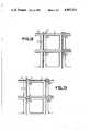
- FIGS. 1 to 7show the different steps of the method in accordance with the invention
- FIG. 8is a perspective view of the component obtained on completion of the step shown in FIG. 4;
- FIG. 9is a perspective view of the component obtained by means of the method in accordance with the invention.
- FIG. 10is a general view of a flat-screen control matrix obtained by means of the method in accordance with the invention.
- FIGS. 11 and 12illustrate an alternative embodiment of the invention
- FIG. 13illustrates another alternative embodiment of the invention.
- FIGS. 1 to 7the different steps of the method in accordance with the invention will now be described.
- a substrate 1such as a glass plate
- a layer 2 of conductive materialwhich can be a transparent material in the event of utilization in a display screen which operates in transparency. It will thus be possible to deposit a thin film of mixed indium-tin oxide (ITO) or an equivalent material (In 2 O 3 , SnO 2 ).
- ITOindium-tin oxide
- a layer of this typewill have a thickness within the range of 500 to 1500 Angstroms, a suitable value being 1250 Anstroms, for example,
- a glass substrate of this type covered with a partially oxidized layer of ITOis commerically available under the trade name of "Baltracon de Balzers", for example.
- the use of a substrate of this typemakes it possible to dispense with this initial step of the method in accordance with the invention.
- the layer 2 of conductive materialis etched in the cold state with a dilute acid so as to form on the surface of the substrate 1 and electrodes 2 such as the electrode which is illustrated in FIG. 1.
- a dilute acidsuch as paritally oxidized ITO lies in the possiblity of employing a dilute acid whereas a totally oxidized ITO would entail the need for hot-state etching by means of a concentrated acid.
- the etching stepis followed by a step of annealing in an ambient atmosphere in order to complete the oxidation of the layer.
- a layer of a metal 3 such as chromiumis deposited by vacuum evaporation or cathode sputtering.
- the thickness of the layer 3must be of the order of a few hundred Angstroms, a suitable value being 600 Angstroms, for example. A structure as shown in FIG. 2 is thus obtained.
- a fourth stepinvolves deposition of a heavily doped n-type layer 4 of semiconductor material such as amorphous silicon.
- This deposition operationis carried out by a known method of deposition of amorphous silicon such as luminescent discharge or reactive sputtering.
- the thickness of this layerwill be approximately 400 Angstroms.
- a structure of the type shown in FIG. 3is thus obtained.
- a fifth stepinvolves etching of the two layers previously deposited (amorphous silicon layer 4 and metal layer 3) in order to form connecting elements CX and columns CL as shown in FIG. 4.
- the connecting element CXis formed by a layer 31 and a layer 41 etched in the layers 3 and 4 of FIG. 3.
- the column CLis constituted by a layer 32 and a layer 42 etched in the layers 3 and 4.
- FIG. 8provides a perspective view of the structure thus obtained.
- the connecting element CXhas the general shape of an L. One of the arms of the L is in contact with the electrode 2 whilst the other arm of the L is parallel to the column CL.
- This etching stepis performed by the photolithographic or photoetching technique and alone serves to define the geometry of the transistor (size of transistor channel).
- a sixth stepinvolves deposition of a layer 5 of semiconductor material such as undoped amorphous silicon. This deposition is performed by a known method such as luminescent discharge or reactive sputtering. The thickness of the layer obtained is approximately 3000 Angstroms. The assembly thus obtained is shown in FIG. 6.
- a seventh stepinvolves deposition of a layer 6 of insulator material (gate insulator) by a method similar to that of the preceding sixth step.
- the thickness of the insulator layer 6is approximately 1500 Angstroms.
- the insulator material employedcan be a nitride, for example.
- An eighth stepinvolves deposition of a layer 7 of metallic material such as aluminum and the like.
- the method of deposition of this layerwill be similar to that of the third step of deposition of layer 3.
- the thickness of layer 7will be approximately 3000 Angstroms.
- a ninth stepinvolves etching of the metal layer 7, the insulator layer 6 and the silicon layer 5 as shown in FIG. 7 in order to obtain row LG.
- the doped silicon of the columns and connecting elementsremains only at the points of intersection with the rows.
- FIG. 9there can be seen a row LG which is perpendicular to the column CL as well as a portion of the connecting element CX. This etching operation is carried out by the photolithographic process.
- the substrate 1which carries electrodes of the rows LG, of the columns CL and of the connecting elements CX at their points of intersection can be employed for the construction of a liquid crystal screen in accordance with known technologies. As has already been demonstrated by practical experience, it will thus prove advisable to provide:
- an anchoring layer(polyimide, SiO, and so on);
- spacers or shimshaving the function of forming a space for containing the liquid crystal
- the liquid crystalwill then be contained between the electrode 2 and a counter-electrode (not shown in the drawings). It will be possible, for example, to observe the liquid crystal between crossed polarizers in the case of a twisted nematic cell.
- a column CL in which a metal layer 32 has higher conductivity than ITOmakes it possible to avoid the effects of delay lines in large-area screens.
- the second step of the process described in the foregoingincludes an operation in which columns of ITO material are also etched along the entire length of the future columns except at the control transistor locations. As shown in FIGS. 11 and 12, a column CL will have a sublayer of ITO over a distance corresponding to the portion shown in hatching lines in FIG. 12.
- each row LGcan be provided with a widened portion at the level of each point of intersection (transistor). This makes it possible to reduce the parasitic transistor effect which may exist between the drain of the principal transistor and the following column.
- the layers of amorphous silicon 5 and of insulating material 6 deposited during the sixth and seventh steps described earliercan be deposited through a mask which serves to isolate the periphery of the substrate 1 from these deposits.
- the peripheral contacts of each row LGare formed directly on the substrate by the deposited metal layer 7.
- the amorphous silicon deposited in the sixth stepcan be electrically compensated or even lightly p-doped in order to reduce photoconductivity and thus to limit the influence of light on the transistor characteristics.
Landscapes
- Physics & Mathematics (AREA)
- Nonlinear Science (AREA)
- Engineering & Computer Science (AREA)
- Microelectronics & Electronic Packaging (AREA)
- Mathematical Physics (AREA)
- Chemical & Material Sciences (AREA)
- Crystallography & Structural Chemistry (AREA)
- General Physics & Mathematics (AREA)
- Optics & Photonics (AREA)
- Liquid Crystal (AREA)
- Thin Film Transistor (AREA)
- Non-Volatile Memory (AREA)
Abstract
Description
Claims (6)
Applications Claiming Priority (2)
| Application Number | Priority Date | Filing Date | Title |
|---|---|---|---|
| FR8512804 | 1985-08-27 | ||
| FR8512804AFR2586859B1 (en) | 1985-08-27 | 1985-08-27 | METHOD FOR MANUFACTURING A CONTROL TRANSISTOR FOR A FLAT VISUALIZATION SCREEN AND CONTROL ELEMENT DERIVED ACCORDING TO THIS METHOD |
Publications (1)
| Publication Number | Publication Date |
|---|---|
| US4697331Atrue US4697331A (en) | 1987-10-06 |
Family
ID=9322434
Family Applications (1)
| Application Number | Title | Priority Date | Filing Date |
|---|---|---|---|
| US06/900,079Expired - Fee RelatedUS4697331A (en) | 1985-08-27 | 1986-08-25 | Method of fabrication of a control transistor for a flat-panel display screen |
Country Status (5)
| Country | Link |
|---|---|
| US (1) | US4697331A (en) |
| EP (1) | EP0216673B1 (en) |
| JP (1) | JPS6252970A (en) |
| DE (1) | DE3672729D1 (en) |
| FR (1) | FR2586859B1 (en) |
Cited By (27)
| Publication number | Priority date | Publication date | Assignee | Title |
|---|---|---|---|---|
| US4728175A (en)* | 1986-10-09 | 1988-03-01 | Ovonic Imaging Systems, Inc. | Liquid crystal display having pixels with auxiliary capacitance |
| US4778258A (en)* | 1987-10-05 | 1988-10-18 | General Electric Company | Protective tab structure for use in the fabrication of matrix addressed thin film transistor liquid crystal displays |
| US4790630A (en)* | 1986-01-27 | 1988-12-13 | Francois Maurice | Active matrix display screen with drain resistance and processes for producing this screen |
| US4792210A (en)* | 1986-01-27 | 1988-12-20 | Francois Maurice | Active matrix display screen with transistor sources connected to adjacent addressing lines and processes for making this screen |
| US4810061A (en)* | 1987-06-24 | 1989-03-07 | Alps Electric Co., Ltd. | Liquid crystal element having conductive wiring part extending from top of transistor light shield to edge |
| US4816885A (en)* | 1986-05-14 | 1989-03-28 | Oki Electric Industry Co., Ltd. | Thin-film transistor matrix for liquid crystal display |
| US4857907A (en)* | 1986-04-30 | 1989-08-15 | 501 Sharp Kabushiki Kaisha | Liquid-crystal display device |
| US4907040A (en)* | 1986-09-17 | 1990-03-06 | Konishiroku Photo Industry Co., Ltd. | Thin film Schottky barrier device |
| US4949141A (en)* | 1988-02-04 | 1990-08-14 | Amoco Corporation | Vertical gate thin film transistors in liquid crystal array |
| US4951113A (en)* | 1988-11-07 | 1990-08-21 | Xerox Corporation | Simultaneously deposited thin film CMOS TFTs and their method of fabrication |
| US4965646A (en)* | 1988-10-21 | 1990-10-23 | General Electric Company | Thin film transistor and crossover structure for liquid crystal displays |
| US5013877A (en)* | 1988-02-08 | 1991-05-07 | Raychem Corporation | Devices for electrical connection |
| US5087113A (en)* | 1988-02-25 | 1992-02-11 | Sharp Kabushiki Kaisha | Liquid crystal display device |
| US5103330A (en)* | 1988-02-16 | 1992-04-07 | Sharp Kabushiki Kaisha | Matrix-type liquid-crystal display panel having redundant conductor structures |
| US5123847A (en)* | 1983-05-11 | 1992-06-23 | Holmberg Scott H | Method of manufacturing flat panel backplanes, display transistors |
| US5132676A (en)* | 1989-05-24 | 1992-07-21 | Ricoh Company, Ltd. | Liquid crystal display |
| US5153142A (en)* | 1990-09-04 | 1992-10-06 | Industrial Technology Research Institute | Method for fabricating an indium tin oxide electrode for a thin film transistor |
| US5191453A (en)* | 1989-08-23 | 1993-03-02 | Nec Corporation | Active matrix substrate for liquid-crystal display and method of fabricating the active matrix substrate |
| US5231039A (en)* | 1988-02-25 | 1993-07-27 | Sharp Kabushiki Kaisha | Method of fabricating a liquid crystal display device |
| US5289300A (en)* | 1991-02-04 | 1994-02-22 | Semiconductor Energy Laboratory Co., Ltd. | Method of manufacturing electro-optical devices wherein the electrode is patterned on the modulation layer |
| US5414283A (en)* | 1993-11-19 | 1995-05-09 | Ois Optical Imaging Systems, Inc. | TFT with reduced parasitic capacitance |
| US5654206A (en)* | 1994-05-13 | 1997-08-05 | International Rectifier Corporation | Amorphous silicon layer for top surface of semiconductor device |
| US5719433A (en)* | 1995-07-25 | 1998-02-17 | Thomson-Csf | Semiconductor component with integrated heat sink |
| US6100950A (en)* | 1997-01-28 | 2000-08-08 | Nec Corporation | Active matrix LCD with thin film transistor switches and method of producing the same |
| US6248634B1 (en)* | 1995-09-26 | 2001-06-19 | Nec Corporation | Field-effect transistor and fabrication method thereof and image display apparatus |
| US20030094611A1 (en)* | 2001-11-14 | 2003-05-22 | Semiconductor Energy Laboratory Co., Ltd | Semiconductor device and method of fabricating the same |
| US20040076742A1 (en)* | 2002-10-22 | 2004-04-22 | Toppoly Optoelectronics Corp. | Method of fabricating reflective liquid crystal display integrated with driving circuit |
Families Citing this family (8)
| Publication number | Priority date | Publication date | Assignee | Title |
|---|---|---|---|---|
| DE68909973T2 (en)* | 1988-03-18 | 1994-03-24 | Seiko Epson Corp | Thin film transistor. |
| JP2678024B2 (en)* | 1988-08-18 | 1997-11-17 | 松下電器産業株式会社 | Image display device Semiconductor device and manufacturing method thereof |
| US5165165A (en)* | 1989-06-02 | 1992-11-24 | Canon Kabushiki Kaisha | Part inserting apparatus and method for use |
| JP3172841B2 (en)* | 1992-02-19 | 2001-06-04 | 株式会社日立製作所 | Thin film transistor, method of manufacturing the same, and liquid crystal display device |
| FR2714766B1 (en)* | 1993-12-30 | 1996-02-02 | France Telecom | Method of manufacturing an active matrix display screen. |
| FR2714765B1 (en)* | 1993-12-30 | 1996-02-02 | France Telecom | Method of making an electrical connection between two conductive layers. |
| FR2718876B1 (en)* | 1994-04-15 | 1998-03-27 | Thomson Lcd | Method for manufacturing a reverse stage TFT. |
| FR2718885B1 (en)* | 1994-04-15 | 1996-07-05 | Thomson Lcd | Method for manufacturing a reverse stage TFT. |
Citations (13)
| Publication number | Priority date | Publication date | Assignee | Title |
|---|---|---|---|---|
| US4332075A (en)* | 1978-05-26 | 1982-06-01 | Matsushita Electric Industrial Co., Ltd. | Method of producing thin film transistor array |
| US4398340A (en)* | 1982-04-26 | 1983-08-16 | The United States Of America As Represented By The Secretary Of The Army | Method for making thin film field effect transistors |
| US4413883A (en)* | 1979-05-31 | 1983-11-08 | Northern Telecom Limited | Displays controlled by MIM switches of small capacitance |
| GB2134685A (en)* | 1982-12-29 | 1984-08-15 | Sharp Kk | Liquid crystal display |
| US4517733A (en)* | 1981-01-06 | 1985-05-21 | Fuji Xerox Co., Ltd. | Process for fabricating thin film image pick-up element |
| US4523811A (en)* | 1981-01-16 | 1985-06-18 | Kabushiki Kaisha Suwa Seikosha | Liquid crystal display matrix including a non-linear device |
| US4543320A (en)* | 1983-11-08 | 1985-09-24 | Energy Conversion Devices, Inc. | Method of making a high performance, small area thin film transistor |
| US4547789A (en)* | 1983-11-08 | 1985-10-15 | Energy Conversion Devices, Inc. | High current thin film transistor |
| US4582395A (en)* | 1980-07-31 | 1986-04-15 | Kabushiki Kaisha Suwa Seikosha | Active matrix assembly for a liquid crystal display device including an insulated-gate-transistor |
| US4609930A (en)* | 1983-05-06 | 1986-09-02 | Seiko Instruments & Electronics Ltd. | Thin film transistor |
| US4625224A (en)* | 1982-01-19 | 1986-11-25 | Canon Kabushiki Kaisha | Thin film transistor having polycrystalline silicon layer with 0.01 to 5 atomic % chlorine |
| US4633284A (en)* | 1983-11-08 | 1986-12-30 | Energy Conversion Devices, Inc. | Thin film transistor having an annealed gate oxide and method of making same |
| US4639087A (en)* | 1984-08-08 | 1987-01-27 | Energy Conversion Devices, Inc. | Displays having pixels with two portions and capacitors |
Family Cites Families (2)
| Publication number | Priority date | Publication date | Assignee | Title |
|---|---|---|---|---|
| JPS56107287A (en)* | 1980-01-31 | 1981-08-26 | Tokyo Shibaura Electric Co | Image display unit |
| FR2533072B1 (en)* | 1982-09-14 | 1986-07-18 | Coissard Pierre | METHOD FOR MANUFACTURING ELECTRONIC CIRCUITS BASED ON THIN FILM TRANSISTORS AND CAPACITORS |
- 1985
- 1985-08-27FRFR8512804Apatent/FR2586859B1/ennot_activeExpired
- 1986
- 1986-08-22EPEP86401863Apatent/EP0216673B1/ennot_activeExpired - Lifetime
- 1986-08-22DEDE8686401863Tpatent/DE3672729D1/ennot_activeExpired - Fee Related
- 1986-08-25USUS06/900,079patent/US4697331A/ennot_activeExpired - Fee Related
- 1986-08-27JPJP61201173Apatent/JPS6252970A/enactivePending
Patent Citations (14)
| Publication number | Priority date | Publication date | Assignee | Title |
|---|---|---|---|---|
| US4332075A (en)* | 1978-05-26 | 1982-06-01 | Matsushita Electric Industrial Co., Ltd. | Method of producing thin film transistor array |
| US4413883A (en)* | 1979-05-31 | 1983-11-08 | Northern Telecom Limited | Displays controlled by MIM switches of small capacitance |
| US4413883B1 (en)* | 1979-05-31 | 1991-06-04 | Northern Telecom Ltd | |
| US4582395A (en)* | 1980-07-31 | 1986-04-15 | Kabushiki Kaisha Suwa Seikosha | Active matrix assembly for a liquid crystal display device including an insulated-gate-transistor |
| US4517733A (en)* | 1981-01-06 | 1985-05-21 | Fuji Xerox Co., Ltd. | Process for fabricating thin film image pick-up element |
| US4523811A (en)* | 1981-01-16 | 1985-06-18 | Kabushiki Kaisha Suwa Seikosha | Liquid crystal display matrix including a non-linear device |
| US4625224A (en)* | 1982-01-19 | 1986-11-25 | Canon Kabushiki Kaisha | Thin film transistor having polycrystalline silicon layer with 0.01 to 5 atomic % chlorine |
| US4398340A (en)* | 1982-04-26 | 1983-08-16 | The United States Of America As Represented By The Secretary Of The Army | Method for making thin film field effect transistors |
| GB2134685A (en)* | 1982-12-29 | 1984-08-15 | Sharp Kk | Liquid crystal display |
| US4609930A (en)* | 1983-05-06 | 1986-09-02 | Seiko Instruments & Electronics Ltd. | Thin film transistor |
| US4547789A (en)* | 1983-11-08 | 1985-10-15 | Energy Conversion Devices, Inc. | High current thin film transistor |
| US4633284A (en)* | 1983-11-08 | 1986-12-30 | Energy Conversion Devices, Inc. | Thin film transistor having an annealed gate oxide and method of making same |
| US4543320A (en)* | 1983-11-08 | 1985-09-24 | Energy Conversion Devices, Inc. | Method of making a high performance, small area thin film transistor |
| US4639087A (en)* | 1984-08-08 | 1987-01-27 | Energy Conversion Devices, Inc. | Displays having pixels with two portions and capacitors |
Non-Patent Citations (4)
| Title |
|---|
| Proceeding of the SiD, vol. 25/1, 1984, pp. 21 24, A Self Alignment Processed a Si: H TFT Matrix Circuit for LCD Panels by S. Kawai et al.* |
| Proceeding of the SiD, vol. 25/1, 1984, pp. 21-24, "A Self-Alignment Processed a-Si: H TFT Matrix Circuit for LCD Panels" by S. Kawai et al. |
| Xerox Disclosure Journal, vol. 9, No. 6, Nov./Dec. 1984, pp. 355 356, Transparent Drain Pads for Liquid Crystal Displays by W. G. Hawkins.* |
| Xerox Disclosure Journal, vol. 9, No. 6, Nov./Dec. 1984, pp. 355-356, "Transparent Drain Pads for Liquid Crystal Displays" by W. G. Hawkins. |
Cited By (35)
| Publication number | Priority date | Publication date | Assignee | Title |
|---|---|---|---|---|
| US5123847A (en)* | 1983-05-11 | 1992-06-23 | Holmberg Scott H | Method of manufacturing flat panel backplanes, display transistors |
| US4790630A (en)* | 1986-01-27 | 1988-12-13 | Francois Maurice | Active matrix display screen with drain resistance and processes for producing this screen |
| US4792210A (en)* | 1986-01-27 | 1988-12-20 | Francois Maurice | Active matrix display screen with transistor sources connected to adjacent addressing lines and processes for making this screen |
| US4857907A (en)* | 1986-04-30 | 1989-08-15 | 501 Sharp Kabushiki Kaisha | Liquid-crystal display device |
| US4816885A (en)* | 1986-05-14 | 1989-03-28 | Oki Electric Industry Co., Ltd. | Thin-film transistor matrix for liquid crystal display |
| US4907040A (en)* | 1986-09-17 | 1990-03-06 | Konishiroku Photo Industry Co., Ltd. | Thin film Schottky barrier device |
| US4728175A (en)* | 1986-10-09 | 1988-03-01 | Ovonic Imaging Systems, Inc. | Liquid crystal display having pixels with auxiliary capacitance |
| US4810061A (en)* | 1987-06-24 | 1989-03-07 | Alps Electric Co., Ltd. | Liquid crystal element having conductive wiring part extending from top of transistor light shield to edge |
| US4778258A (en)* | 1987-10-05 | 1988-10-18 | General Electric Company | Protective tab structure for use in the fabrication of matrix addressed thin film transistor liquid crystal displays |
| US4949141A (en)* | 1988-02-04 | 1990-08-14 | Amoco Corporation | Vertical gate thin film transistors in liquid crystal array |
| US5013877A (en)* | 1988-02-08 | 1991-05-07 | Raychem Corporation | Devices for electrical connection |
| US5103330A (en)* | 1988-02-16 | 1992-04-07 | Sharp Kabushiki Kaisha | Matrix-type liquid-crystal display panel having redundant conductor structures |
| US5087113A (en)* | 1988-02-25 | 1992-02-11 | Sharp Kabushiki Kaisha | Liquid crystal display device |
| US5231039A (en)* | 1988-02-25 | 1993-07-27 | Sharp Kabushiki Kaisha | Method of fabricating a liquid crystal display device |
| US4965646A (en)* | 1988-10-21 | 1990-10-23 | General Electric Company | Thin film transistor and crossover structure for liquid crystal displays |
| US4951113A (en)* | 1988-11-07 | 1990-08-21 | Xerox Corporation | Simultaneously deposited thin film CMOS TFTs and their method of fabrication |
| US5132676A (en)* | 1989-05-24 | 1992-07-21 | Ricoh Company, Ltd. | Liquid crystal display |
| US5300449A (en)* | 1989-08-23 | 1994-04-05 | Nec Corporation | Active matrix substrate for liquid-crystal display and method of fabricating the active matrix substrate |
| US5191453A (en)* | 1989-08-23 | 1993-03-02 | Nec Corporation | Active matrix substrate for liquid-crystal display and method of fabricating the active matrix substrate |
| US5153142A (en)* | 1990-09-04 | 1992-10-06 | Industrial Technology Research Institute | Method for fabricating an indium tin oxide electrode for a thin film transistor |
| US5289300A (en)* | 1991-02-04 | 1994-02-22 | Semiconductor Energy Laboratory Co., Ltd. | Method of manufacturing electro-optical devices wherein the electrode is patterned on the modulation layer |
| US5414283A (en)* | 1993-11-19 | 1995-05-09 | Ois Optical Imaging Systems, Inc. | TFT with reduced parasitic capacitance |
| US5614427A (en)* | 1993-11-19 | 1997-03-25 | Ois Optical Imaging Systems, Inc. | Method of making an array of TFTs having reduced parasitic capacitance |
| US5654206A (en)* | 1994-05-13 | 1997-08-05 | International Rectifier Corporation | Amorphous silicon layer for top surface of semiconductor device |
| US5719433A (en)* | 1995-07-25 | 1998-02-17 | Thomson-Csf | Semiconductor component with integrated heat sink |
| US6248634B1 (en)* | 1995-09-26 | 2001-06-19 | Nec Corporation | Field-effect transistor and fabrication method thereof and image display apparatus |
| US6100950A (en)* | 1997-01-28 | 2000-08-08 | Nec Corporation | Active matrix LCD with thin film transistor switches and method of producing the same |
| US20030094611A1 (en)* | 2001-11-14 | 2003-05-22 | Semiconductor Energy Laboratory Co., Ltd | Semiconductor device and method of fabricating the same |
| US7238557B2 (en)* | 2001-11-14 | 2007-07-03 | Semiconductor Energy Laboratory Co., Ltd. | Semiconductor device and method of fabricating the same |
| US20070228374A1 (en)* | 2001-11-14 | 2007-10-04 | Semiconductor Energy Laboratory Co., Ltd. | Semiconductor device and method of fabricating the same |
| US7834356B2 (en) | 2001-11-14 | 2010-11-16 | Semiconductor Energy Laboratory Co., Ltd. | Semiconductor device and method of fabricating the same |
| US20110034009A1 (en)* | 2001-11-14 | 2011-02-10 | Semiconductor Energy Laboratory Co., Ltd. | Semiconductor device and method of fabricating the same |
| US8043905B2 (en) | 2001-11-14 | 2011-10-25 | Semiconductor Energy Laboratory Co., Ltd. | Semiconductor device and method of fabricating the same |
| US20040076742A1 (en)* | 2002-10-22 | 2004-04-22 | Toppoly Optoelectronics Corp. | Method of fabricating reflective liquid crystal display integrated with driving circuit |
| US7115431B2 (en)* | 2002-10-22 | 2006-10-03 | Tpo Displays Corp. | Method of fabricating reflective liquid crystal display integrated with driving circuit |
Also Published As
| Publication number | Publication date |
|---|---|
| JPS6252970A (en) | 1987-03-07 |
| DE3672729D1 (en) | 1990-08-23 |
| EP0216673B1 (en) | 1990-07-18 |
| FR2586859B1 (en) | 1987-11-20 |
| FR2586859A1 (en) | 1987-03-06 |
| EP0216673A1 (en) | 1987-04-01 |
Similar Documents
| Publication | Publication Date | Title |
|---|---|---|
| US4697331A (en) | Method of fabrication of a control transistor for a flat-panel display screen | |
| US5041888A (en) | Insulator structure for amorphous silicon thin-film transistors | |
| US5498573A (en) | Method of making multi-layer address lines for amorphous silicon liquid crystal display devices | |
| US4653858A (en) | Method of fabrication of diode-type control matrices for a flat electrooptical display screen and a flat screen constructed in accordance with said method | |
| US9881942B2 (en) | Array substrate, manufacturing method thereof and display device | |
| US6180438B1 (en) | Thin film transistors and electronic devices comprising such | |
| US5874326A (en) | Method for fabricating thin film transistor | |
| US5231039A (en) | Method of fabricating a liquid crystal display device | |
| US5087113A (en) | Liquid crystal display device | |
| CN101123257A (en) | Thin film transistor array base plate and its making method | |
| US4732873A (en) | Method of fabrication of non-linear control elements for a flat electrooptical display screen | |
| JP3099274B2 (en) | Wide viewing angle type active matrix liquid crystal display device having halftone gray scale and method of manufacturing the same | |
| US20070024770A1 (en) | Liquid crystal display device and method of fabricating the same | |
| KR20010015187A (en) | Thin film transistor array and its manufacturing method | |
| US4810637A (en) | Non-linear control element for a flat electrooptical display screen and a method of fabrication of said control element | |
| JPH01217422A (en) | Amorphous silicon thin film transistor array substrate | |
| US4944575A (en) | Electrooptical display screen and a method of fabrication of said screen | |
| US5677547A (en) | Thin film transistor and display device including same | |
| US20040245523A1 (en) | Circular thin film transistor structure | |
| EP0721213A2 (en) | Array with metal scan lines controlling semiconductor gate lines | |
| US5061040A (en) | Liquid crystal displays operated by amorphous silicon alloy diodes | |
| US6757033B2 (en) | Liquid crystal display device and method for manufacturing the same | |
| US20050225543A1 (en) | Display circuit having asymmetrical nonlinear resistive elements | |
| EP0150798B1 (en) | Liquid crystal displays operated by amorphous silicon alloy diodes | |
| KR0120399Y1 (en) | Liquid crystal display device |
Legal Events
| Date | Code | Title | Description |
|---|---|---|---|
| AS | Assignment | Owner name:THOMSON-CSF, 173, B1. HAUSSMANN 75008 PARIS FRANCE Free format text:ASSIGNMENT OF ASSIGNORS INTEREST.;ASSIGNORS:BOULITROP, FRANCOIS;CHARTIER, ERIC;MOUREY, BRUNO;AND OTHERS;REEL/FRAME:004737/0219 Effective date:19860813 Owner name:THOMSON-CSF, FRANCE Free format text:ASSIGNMENT OF ASSIGNORS INTEREST;ASSIGNORS:BOULITROP, FRANCOIS;CHARTIER, ERIC;MOUREY, BRUNO;AND OTHERS;REEL/FRAME:004737/0219 Effective date:19860813 | |
| FEPP | Fee payment procedure | Free format text:MAINTENANCE FEE HAS ALREADY BEEN PAID. REFUND IS SCHEDULED (ORIGINAL EVENT CODE: F160); ENTITY STATUS OF PATENT OWNER: LARGE ENTITY | |
| FEPP | Fee payment procedure | Free format text:PAYOR NUMBER ASSIGNED (ORIGINAL EVENT CODE: ASPN); ENTITY STATUS OF PATENT OWNER: LARGE ENTITY | |
| FPAY | Fee payment | Year of fee payment:4 | |
| FEPP | Fee payment procedure | Free format text:PAYOR NUMBER ASSIGNED (ORIGINAL EVENT CODE: ASPN); ENTITY STATUS OF PATENT OWNER: LARGE ENTITY Free format text:PAYER NUMBER DE-ASSIGNED (ORIGINAL EVENT CODE: RMPN); ENTITY STATUS OF PATENT OWNER: LARGE ENTITY | |
| FPAY | Fee payment | Year of fee payment:8 | |
| REMI | Maintenance fee reminder mailed | ||
| LAPS | Lapse for failure to pay maintenance fees | ||
| FP | Lapsed due to failure to pay maintenance fee | Effective date:19991006 | |
| STCH | Information on status: patent discontinuation | Free format text:PATENT EXPIRED DUE TO NONPAYMENT OF MAINTENANCE FEES UNDER 37 CFR 1.362 |