US4691176A - Adaptive carrier tracking circuit - Google Patents
Adaptive carrier tracking circuitDownload PDFInfo
- Publication number
- US4691176A US4691176AUS06/840,220US84022086AUS4691176AUS 4691176 AUS4691176 AUS 4691176AUS 84022086 AUS84022086 AUS 84022086AUS 4691176 AUS4691176 AUS 4691176A
- Authority
- US
- United States
- Prior art keywords
- signal
- output
- input
- coupled
- phase
- Prior art date
- Legal status (The legal status is an assumption and is not a legal conclusion. Google has not performed a legal analysis and makes no representation as to the accuracy of the status listed.)
- Expired - Fee Related
Links
- 230000003044adaptive effectEffects0.000titleclaimsabstractdescription105
- 238000005070samplingMethods0.000claimsdescription17
- 230000010363phase shiftEffects0.000claimsdescription13
- 230000003111delayed effectEffects0.000claimsdescription8
- 238000001914filtrationMethods0.000claims1
- 238000004891communicationMethods0.000abstractdescription7
- 238000004422calculation algorithmMethods0.000description3
- 239000000047productSubstances0.000description3
- 238000004364calculation methodMethods0.000description2
- 230000001427coherent effectEffects0.000description2
- 238000012937correctionMethods0.000description2
- 230000003466anti-cipated effectEffects0.000description1
- 239000003990capacitorSubstances0.000description1
- 239000005433ionosphereSubstances0.000description1
- 238000005259measurementMethods0.000description1
- 238000000034methodMethods0.000description1
- 238000012986modificationMethods0.000description1
- 230000004048modificationEffects0.000description1
- 238000012544monitoring processMethods0.000description1
- 230000000644propagated effectEffects0.000description1
- 230000008929regenerationEffects0.000description1
- 238000011069regeneration methodMethods0.000description1
- 238000006467substitution reactionMethods0.000description1
- 239000013589supplementSubstances0.000description1
Images


Classifications
- H—ELECTRICITY
- H03—ELECTRONIC CIRCUITRY
- H03L—AUTOMATIC CONTROL, STARTING, SYNCHRONISATION OR STABILISATION OF GENERATORS OF ELECTRONIC OSCILLATIONS OR PULSES
- H03L7/00—Automatic control of frequency or phase; Synchronisation
- H03L7/06—Automatic control of frequency or phase; Synchronisation using a reference signal applied to a frequency- or phase-locked loop
- H03L7/07—Automatic control of frequency or phase; Synchronisation using a reference signal applied to a frequency- or phase-locked loop using several loops, e.g. for redundant clock signal generation
- H—ELECTRICITY
- H03—ELECTRONIC CIRCUITRY
- H03L—AUTOMATIC CONTROL, STARTING, SYNCHRONISATION OR STABILISATION OF GENERATORS OF ELECTRONIC OSCILLATIONS OR PULSES
- H03L7/00—Automatic control of frequency or phase; Synchronisation
- H03L7/06—Automatic control of frequency or phase; Synchronisation using a reference signal applied to a frequency- or phase-locked loop
- H03L7/08—Details of the phase-locked loop
- H03L7/085—Details of the phase-locked loop concerning mainly the frequency- or phase-detection arrangement including the filtering or amplification of its output signal
- H03L7/087—Details of the phase-locked loop concerning mainly the frequency- or phase-detection arrangement including the filtering or amplification of its output signal using at least two phase detectors or a frequency and phase detector in the loop
Definitions
- the present inventionrelates in general to communication systems and more particularly to an improved carrier tracking circuit for a pulse code modulation communication system.
- Demodulators intended for both on-board and on ground satellite communicationshave typically used regeneration of a carrier by a phase-locked loop to demodulate an RF signal.
- the primary concerns in use of such a systemare to maintain signal tracking and to minimize bit error rates. This involves a tradeoff.
- a narrow filter bandwidth in the phase-locked loopis desirable for its ability to reject large amounts of noise, thus resulting in a more stable regenerated carrier. Usually this presents no problem if the original signal is stable both as to frequency and phase.
- a larger filter bandwidthis required to track the signal in its entirety and minimize the bit error rate.
- Prior art devicesprovide tracking circuits having adjustable bandwidths with a wide range of values.
- the settingsare performed manually by an operator and are based on detected signal quality. In a rapidly changing environment, manual adjustment may be too slow or too late, resulting at least in degraded performance and, at worst, in a loss of signal lock.
- the foregoing objects of the inventionare achieved by the use of a new and improved adaptive carrier tracking circuit for receiving pulse code modulated communications which are propagated through a disturbed or scintillation environment before being received.
- the tracking circuit of the present inventionis capable of adjusting a loop filter bandwidth to optimize signal tracking during such fluctuations and to minimize noise when the input signal is relatively stable.
- the present inventionmay be applied to communication systems tracking loops utilizing phase-locked loops or modified Costas loops for phase tracking, or automatic frequency control (AFC) loops for frequency tracking.
- the basis of the present inventionis that information contained in a phase or frequency error signal of a carrier tracking circuit can be used to dynamically adjust the parameters of the circuit during times of rapid phase or frequency fluctuations to optimize performance of the circuit. Either the tracking circuit itself or a secondary tracking circuit or loop is used to generate the error signal.
- thisis achieved with a phase tracking circuit by using first and second modified Costas loops coupled to the input signal.
- the first modified Costas loopincludes a narrow bandwidth filter and operates in conjunction with a channel characteristic estimator to estimate an input signal decorrelation time and to adjust an adaptive filter bandwidth of the second modified Costas loop.
- the estimatordetects the frequency of the input signal as well as the magnitude and rate of phase fluctuations of the input signal from the output signal of the first modified Costas loop and computes the optimum filter bandwidth for the second modified Costas loop.
- the baseband signal provided by the second loopis coupled to a phase shift keying demodulator.
- Dynamic adjustment of the bandwidth of the adaptive filter of the second modified Costas loopallows a minimized noise level or noise bandwidth, and thus a minimized bit error rate, at times when the input signal has passed through a benign environment. It also provides tracking assurance and minimized bit error rates when the signal passes through a scintillation environment. Because the response time of the estimator is short and is determined by the timing interval used, the present invention is capable of responding to phase and frequency fluctuations which are too rapid for correction by manual adjustments.
- FIGS. 1 and 2show schematic representations of the present invention for phase tracking implemented with phase-locked loops
- FIG. 3shows a schematic representation of the present invention for phase tracking implemented with modified Costas loops
- FIG. 4shows another embodiment of the present invention for phase tracking implemented with modified Costas loop
- FIG. 5is a schematic representation of the channel characteristic estimator used in the embodiments of FIGS. 1-4.
- FIG. 6shows a schematic representation of the present invention for frequency tracking implemented with an automatic frequency control loop.
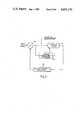
- FIG. 1shows one embodiment of an adaptive carrier tracking circuit as an adaptive phase-locked loop including first and second loops 6 and 8 respectively.
- Second loop 8includes a phase detector 10 which receives an externally derived input signal and has its output which is a phase error signal coupled to a narrow bandwidth filter 12.
- Filter 12provides a restoring error signal at its output which is fed to a voltage controlled oscillator 14.
- the latterprovides a reference signal to phase detector 10 in response to the restoring error signal.
- the phase error signal derived at the output of phase detector 10is proportional to the phase difference or error between the input signal and the reference signal from voltage controlled oscillator 14.
- the number of reversals or zero-crossings of this phase difference signalis a measure of the rate of phase fluctuations of the input signal.
- This phase difference signal from phase detector 10constitutes the output signal of loop 8 and it is applied to a channel characteristic estimator 16.
- Second loop 6includes a phase detector 18 which receives the aforesaid input signal.
- the output of phase detector 18is coupled to an adaptive filter 20.
- Filter 20has an adjustable bandwidth and its output is coupled to a second voltage controlled oscillator 22 which provides a reference signal to phase detector 18.
- Adaptive filter 20receives a control signal from estimator 16 which is capable of varying the bandwidth of filter 20.
- the signal derived at the output of phase detector 18is a baseband signal of the input signal and is further fed to a demodulator which decodes the input signal.
- estimator 16 and loop 8jointly function as a detector for monitoring the characteristics of phase fluctuations and particularly the rate of fluctuations of the input signal. Adjustments are made to the bandwidth of adaptive filter 20 in response to such fluctuations in order to optimize the performance of tracking loop 6.
- the bandwidth selectedis a function of the frequency of the input signal and of the rate and magnitude of phase fluctuations.
- the criterion for optimum performanceis minimum noise in the output signal that is provided to the demodulator in order to minimize the bit error rate of the system. Such noise is minimized by adjusting the bandwidth of the adaptive filter to the minimum acceptable value at times when the input signal is stable.
- estimator 16uses the root mean square (r.m.s.) average of the magnitude of phase error and the number of zero-crossings of the difference signal during a given timing interval, which may be on the order of about one second, estimator 16 computes a decorrelation time which is a measure of the rate of fluctuations of a given magnitude.
- An optimum filter bandwidth for adaptive filter 20is determined based on the computed decorrelation time. The algorithm for determining the filter bandwidth from the decorrelation time uses statistical data for the particular tracking loop involved.
- Estimator 16adjusts the adaptive filter bandwidth such that, for decorrelation times greater than a given predetermined value t max , a minimum bandwidth is set. For decorrelation times less than a given predetermined value t min , the maximum adaptive filter bandwidth is set. For decorrelation times between t min and t max , the loop bandwidth is varied between the minimum and maximum values such that optimum tradeoff between trackability and minimum noise results.
- the available values of the adjusted bandwidthmay be along a continuum, or they may be discrete values.
- the bandwidth of the adaptive filtermay be varied by adjusting the values of resistors and capacitors comprising the filter. Alternatively, or as a supplement, the gain of phase detector 18, or of voltage controlled oscillator 22, may be adjusted.
- FIG. 2A second embodiment of the adaptive carrier tracking circuit as an adaptive phase-locked loop is shown schematically in FIG. 2 and is seen to consist of a single loop.
- This loopincludes a phase detector 30 which provides a phase error signal at its output. The latter output is coupled to an adaptive filter 32 which, in turn, has its output coupled to a voltage controlled oscillator 34.
- Oscillator 34receives a restoring error signal from adaptive filter 32 and provides a responsive reference signal to phase detector 30.
- a channel characteristic estimator 36is connected to the output of phase detector 30.
- the embodiment illustrated in FIG. 2adjusts the adaptive filter bandwidth based on computational algorithms utilizing measurements of the characteristics of the output signal and the present setting of the adaptive circuit. While such an arrangement requires fewer components for the adaptive carrier tracking circuit than the embodiment of FIG. 1, estimator 36 must factor in that the tracking errors of the measured signal of the adaptive circuit are smaller than those used to measure the characteristics in the embodiment of FIG. 1. This is because the dynamic adjustment of the filter bandwidth affects loop performance to reduce tracking errors.
- FIG. 3illustrates an embodiment of the present invention employing the adaptive carrier tracking circuit techniques for an input circuit of the type used with either a coherent phase shift keying (CPSK) demodulator, or a differential phase shift keying (DPSK) demodulator.
- the present embodimentuses first and second modified Costas loops, designated 40 and 60 respectively.
- a modified Costas loopincludes an integrate-and-dump circuit following each of the two input mixers.
- First loop 40includes a pair of mixers 42 and 44, both of which are coupled to receive the input signal.
- a voltage controlled oscillator 46provides an inphase reference signal at its output which is coupled to mixer 42.
- a 90° phase-shift element 48is further coupled to the output of oscillator 46 and provides a quadrature reference signal to mixer 44.
- the outputs of mixers 42 and 44 of loop 40are coupled to integrate-and-dump circuits 50 and 52 respectively, which function as low pass filters for the signals derived at the mixer outputs.
- Circuit 50is followed by a signum (Sgn) element 54 which provides an output of ⁇ one, depending on whether the signal it receives is greater or less than zero.
- a mixer 56is coupled to receive inputs from element 54 and circuit 52.
- Mixer 56provides a phase error signal at its output which is a product of the signals received at its inputs.
- a narrow bandwidth filter 58is coupled to the output of mixer 56 and provides a restoring error signal to voltage controlled oscillator 46.
- Loop 60is configured essentially the same as loop 40.
- a pair of mixers 62 and 64receive the input signal and they are followed by a pair of integrate-and-dump circuits 70 and 72 respectively.
- a voltage controlled oscillator 66provides an inphase reference signal to mixer 62 and, through a 90° phase-shift element 68, a quadrature reference signal to mixer 64.
- Circuit 70is followed by a Sgn element 74 and its output is mixed with the output of circuit 72 by means of a mixer 76 to provide a phase error signal.
- An adaptive filter 78receives the phase error signal from mixer 76 and provides a restoring error signal to oscillator 66.
- a channel characteristic estimator 80is coupled between the output of mixer 56 and adaptive filter 78 and provides a control signal for varying the bandwidth of filter 78.
- FIG. 5illustrates a channel characteristic estimator, such as is shown in each of FIGS. 1-4, in greater detail.
- the channel characteristic estimatoris discussed here with reference to estimator 80 shown in FIG. 3.
- the signal derived at the output of mixer 56is applied to a circuit for calculating the r.m.s. phase error 82 and to a zero crossing counter 84.
- a timing circuit 86is coupled to calculating circuit 82 and to counter 84 to control the sampling or timing interval.
- the outputs of calculating circuit 82 and of counter 84are fed to an analog-to-digital converter 88, which in turn is coupled to a microprocessor 90.
- Timing circuit 86is coupled to microprocessor 90, which additionally receives a signal from an external automatic gain control (AGC) circuit.
- AGCautomatic gain control
- Microprocessor 90provides a computed control signal at its output for varying the bandwidth of adaptive filter 78.
- loop 40which includes narrow bandwidth filter 58, functions as a detector for tracking errors, its output signal being fed to estimator 80.
- the information in the aforesaid loop output signalincludes data concerning the frequency of the input signal, as well as rate and magnitude of phase variations of this signal over a given sampling period.
- a decorrelation timeis estimated by microprocessor 90 and, based on this data, an optimum bandwidth for the particular circuit is calculated to provide a minimum bit error rate.
- the input signal, A(t) cos ⁇ I (t),is adjusted by the AGC circuit before being fed to the carrier tracking circuit.
- This input signalis mixed with the inphase reference signals from voltage controlled oscillators 46 and 66 by means of mixers 42 and 62 respectively.
- the input signalis further mixed with the quadrature reference signals from phase-shift elements 48 and 68 by means of mixers 44 and 64 respectively.
- the mixer productsare filtered by integrate-and-dump circuits 50, 52, 70 and 72 which follow mixers 42, 44, 62 and 64, respectively.
- the output signals of circuits 50 and 70constitute inphase samples I k of the baseband signal.
- the outputs of circuits 52 and 72constitute quadrature samples Q k of the baseband signal.
- ⁇ kis defined as the phase error at t k and equals the difference between the input signal phase ⁇ I (t k ) and the voltage controlled oscillator reference signal phase ⁇ R (t k ).
- phase error signal e kwhich drives each voltage controlled oscillator is represented by:
- the value of the phase error signalis related to the frequency of the input signal and to the rate and magnitude of phase variations of the input signal over a given sampling time.
- Estimator 80uses the information contained in the restoring error signal from loop 40 to estimate the input signal decorrelation time and to calculate an optimum bandwidth for adaptive loop filter 78.
- the r.m.s. phase error averaged over the timing intervalis estimated from the phase error signal by calculating means 82 (FIG. 5).
- the periodicity of the phase erroris determined from the phase error signal by zero crossing counter 84 (FIG. 5) for the same timing interval. It should be noted here that the timing interval provided by timing circuit 86 (FIG. 5) is adjustable and is set based on the rate of fluctuations anticipated for a given circuit application.
- a typical timing intervalmay be on the order of one second.
- the data described aboveis provided to microprocessor 90 (FIG. 5) via analog-to-digital converter 88 (FIG. 5), along with an address to identify the particular timing interval involved.
- Microprocessor 90then calculates the average magnitude of phase error and interval of phase fluctuations and computes a bandwidth for adaptive filter 78 to provide optimum performance for the signal conditions existing during the timing interval. In making the calculation, microprocessor 90 also takes into consideration any adjustments made to the input signal by the AGC circuit. This prevents erroneous adjustments of the adaptive filter bandwidth where the input signal is of a very low magnitude as compared to the noise level.
- a second configuration of the adaptive carrier tracking circuit which uses a modified Costas loopis shown in FIG. 4.
- the input signalis fed to a pair of mixers 100 and 102.
- a voltage controlled oscillator 104provides an inphase reference signal to mixer 100 and, through 90° phase-shift element 106, a quadrature reference signal to mixer 102.
- the outputs of mixers 100 and 102are coupled to integrate-and-dump circuits 108 and 110 respectively.
- the output of circuit 108is fed to Sgn element 112.
- the signal derived at the output of element 112is coupled to a mixer 114 along with the output signal of circuit 110.
- the restoring error signal derived at the output of mixer 114is coupled to an adaptive filter 116 which has an adjustable bandwidth.
- a channel characteristic estimator 118is also coupled to the output of mixer 114 and receives the phase error signal.
- Filter 116provides a filtered restoring error signal to a voltage controlled oscillator 104.
- Estimator 118provides a control signal to filter 116 adapted to vary its bandwidth.
- Filter 116is further coupled to the microprocessor of estimator 118 to provide the current setting of the adaptive filter bandwidth.
- the tracking circuit shown in FIG. 4functions analogously to the embodiment of FIG. 2 in that channel characteristic estimator 118 uses the phase error signal from the tracking loop for providing input signal phase fluctuction information.
- An inphase sample I k of the baseband signalis provided at the output of circuit 108 and a quadrature sample Q k of the baseband signal is provided at the output of circuit 110.
- Mixer 114then provides the phase error signal e k as a product of the quadrature sample with the sign of the inphase sample as shown by the following relationship:
- This error signalis used by estimator 118 to determine the optimum bandwidth for adaptive filter 116.
- the most recent bandwidth setting of filter 116is used by the microprocessor of estimator 118 since that bandwidth setting affects the circuit tracking performance.
- the present inventioncan also be used with a carrier tracking circuit which utilizes frequency tracking of the input signal, as shown in FIG. 6.
- the frequency error signal f k of an automatic frequency control (AFC) circuitis used for determining input signal fluctuation characteristics.
- the AFC circuitincludes a pair of mixers 120 and 122 coupled to receive the input signal.
- a voltage controlled oscillator 124provides an inphase reference signal at its output which is coupled to mixer 120.
- a 90° phase-shift element 126is further coupled to the output of oscillator 124 and provides a quadrature reference signal to mixer 122.
- the signals provided at the outputs of mixers 120 and 122are inphase sample I k and quadrature sample Q k of the baseband signal which are coupled to a pair of integrate-and-dump circuits 128 and 130 respectively.
- the integrate-and-dump circuitsfunction as low pass filters for the inphase and quadrature samples derived at the mixer outputs.
- Circuits 128 and 130are followed by sample delay elements 132 and 134 respectively, which provide time delayed inphase sample I k-1 and time delayed quadrature sample Q k-1 respectively.
- a mixer 136is coupled to receive the delayed inphase sample I k-1 from element 132 and the quadrature sample Q k from the output of circuit 130.
- a mixer 138is coupled to receive the time delayed quadrature Q k-1 sample from element 134 and the inphase sample I k from the output of circuit 128.
- a difference mixer 140is coupled to the outputs of mixers 136 and 138 to provide a frequency error signal which represents the difference of the signals from mixers 136 and 138 such that:
- f kis the frequency error signal
- An adaptive filter 142having an adjustable bandwidth, is coupled to receive the frequency error signal and provide a restoring error signal to oscillator 124.
- a channel characteristic estimator 144is coupled to receive the frequency error signal and provide a responsive control signal for varying the bandwidth of adaptive filter 142.
- Estimator 144functions in essentially the same manner as the estimator shown in FIG. 5 for use with phase tracking circuits, except that it measures the rate and magnitude of frequency fluctuations of the input signal.
- the output signal of the AFC circuitis either the inphase sample I k from the output of circuit 128 or the quadrature sample Q k from the output of circuit 130. This signal is applied to a phase shift keying demodulator.
- An alternative embodiment of the present invention for frequency trackingemploys a second AFC circuit as a detector to provide the frequency error signal to the channel characteristic estimator. This embodiment is comparable to the phase tracking embodiment shown in FIG. 3.
- the adaptive carrier tracking circuithas been described with reference to phase or frequency tracking of a pulse code modulated input signal and a phase shift keying demodulator.
- the present inventionmay be used with demodulators for other kinds of modulated signals such as, for example, coherent amplitude detectors, phase demodulators and frequency demodulators.
- the present inventionmay be used where the source of tracking errors is other than a scintillation environment such as, for example, a changing doppler shift environment of a moving platform.
Landscapes
- Stabilization Of Oscillater, Synchronisation, Frequency Synthesizers (AREA)
- Digital Transmission Methods That Use Modulated Carrier Waves (AREA)
Abstract
Description
I.sub.k =A (t.sub.k) cos φ.sub.k
Q.sub.k =A (t.sub.k) sin φ.sub.k
e.sub.k =Q.sub.k Sgn (I.sub.k).
e.sub.k =Q.sub.k Sgn (I.sub.k).
f.sub.k =Q.sub.k I.sub.k-1 -I.sub.k Q.sub.k-1
Claims (16)
Priority Applications (1)
| Application Number | Priority Date | Filing Date | Title |
|---|---|---|---|
| US06/840,220US4691176A (en) | 1986-03-17 | 1986-03-17 | Adaptive carrier tracking circuit |
Applications Claiming Priority (1)
| Application Number | Priority Date | Filing Date | Title |
|---|---|---|---|
| US06/840,220US4691176A (en) | 1986-03-17 | 1986-03-17 | Adaptive carrier tracking circuit |
Publications (1)
| Publication Number | Publication Date |
|---|---|
| US4691176Atrue US4691176A (en) | 1987-09-01 |
Family
ID=25281765
Family Applications (1)
| Application Number | Title | Priority Date | Filing Date |
|---|---|---|---|
| US06/840,220Expired - Fee RelatedUS4691176A (en) | 1986-03-17 | 1986-03-17 | Adaptive carrier tracking circuit |
Country Status (1)
| Country | Link |
|---|---|
| US (1) | US4691176A (en) |
Cited By (39)
| Publication number | Priority date | Publication date | Assignee | Title |
|---|---|---|---|---|
| US4901319A (en)* | 1988-03-18 | 1990-02-13 | General Electric Company | Transmission system with adaptive interleaving |
| US5029162A (en)* | 1990-03-06 | 1991-07-02 | Confertech International | Automatic gain control using root-mean-square circuitry in a digital domain conference bridge for a telephone network |
| US5042052A (en)* | 1990-02-16 | 1991-08-20 | Harris Corporation | Carrier acquisition scheme for QAM and QPSK data |
| US5107521A (en)* | 1989-11-13 | 1992-04-21 | Hughes Aircraft Company | Single analog path multi-data rate matched filtered demodulator |
| US5216698A (en)* | 1991-04-05 | 1993-06-01 | Thomson-Csf | Automatic device for the phase-locking of a circuit |
| DE4292274T1 (en)* | 1991-06-28 | 1993-07-15 | Motorola, Inc., Schaumburg, Ill., Us | |
| US5432521A (en)* | 1994-01-14 | 1995-07-11 | Motorola, Inc. | Satellite receiver system having doppler frequency shift tracking |
| US5481573A (en)* | 1992-06-26 | 1996-01-02 | International Business Machines Corporation | Synchronous clock distribution system |
| WO1996003827A1 (en)* | 1994-07-25 | 1996-02-08 | Motorola Inc. | Apparatus and method for maximizing frequency offset tracking performance in a digital receiver |
| US5703597A (en)* | 1995-12-22 | 1997-12-30 | Alliedsignal, Inc. | Adaptive carrier phase lock loop in a GPS receiver |
| US5789987A (en)* | 1996-01-22 | 1998-08-04 | Motorola, Inc. | Low-noise frequency synthesizer |
| US5815540A (en)* | 1993-06-02 | 1998-09-29 | Nec Corporation | Semiconductor integrated circuit device including PLL circuit |
| US5841811A (en)* | 1994-10-07 | 1998-11-24 | Massachusetts Institute Of Technology | Quadrature sampling system and hybrid equalizer |
| US5909148A (en)* | 1996-04-26 | 1999-06-01 | Nec Corporation | Carrier phase synchronizing circuit |
| US5949832A (en)* | 1996-03-26 | 1999-09-07 | Sicom, Inc. | Digital receiver with tunable analog filter and method therefor |
| WO1999054818A1 (en)* | 1998-04-17 | 1999-10-28 | Ameritech Corporation | Method and system for adaptive interleaving |
| US6049255A (en)* | 1998-06-05 | 2000-04-11 | Telefonaktiebolaget Lm Ericsson | Tuning the bandwidth of a phase-locked loop |
| US6049573A (en)* | 1997-12-11 | 2000-04-11 | Massachusetts Institute Of Technology | Efficient polyphase quadrature digital tuner |
| US6058147A (en)* | 1997-03-03 | 2000-05-02 | Telogy Networks, Inc. | Intelligent carrier acquisition method for satellite communications |
| US6067328A (en)* | 1996-12-12 | 2000-05-23 | Alliedsignal | High precision hardware carrier frequency and phase aiding in a GPS receiver |
| WO2000051237A1 (en)* | 1999-02-26 | 2000-08-31 | Motorola Limited | Frequency tracking loop and method of frequency tracking |
| US6411661B1 (en)* | 1999-05-07 | 2002-06-25 | The Aerospace Corporation | Digital timing recovery loop for GMSK demodulators |
| US20050041724A1 (en)* | 2001-10-17 | 2005-02-24 | Mangesh Chansarkar | Variable bandwidth code-tracking loop with improved signal dynamics loop noise and sensitivity |
| US20050157820A1 (en)* | 2004-01-15 | 2005-07-21 | Supat Wongwirawat | Digital receiver having adaptive carrier recovery circuit |
| US7062004B1 (en)* | 2001-06-06 | 2006-06-13 | Silicon Image, Inc. | Method and apparatus for adaptive control of PLL loop bandwidth |
| US20070110186A1 (en)* | 2005-11-14 | 2007-05-17 | Ibiquity Digital Corporation | Carrier tracking for AM in-band on-channel radio receivers |
| US20080008268A1 (en)* | 2006-07-07 | 2008-01-10 | Ut-Va Koc | Recursive phase estimation for a phase-shift-keying receiver |
| US20080291992A1 (en)* | 2007-05-23 | 2008-11-27 | Mediatek Inc. | System and method of detecting burst noise and minimizing the effect of burst noise |
| US7620154B2 (en) | 2002-12-23 | 2009-11-17 | Cambron G Keith | Equivalent working length determinative system for digital subscriber line circuits |
| US20100070208A1 (en)* | 2008-09-18 | 2010-03-18 | Enraf B.V. | Apparatus and method for dynamic peak detection, identification, and tracking in level gauging applications |
| US20100066589A1 (en)* | 2008-09-18 | 2010-03-18 | Enraf B.V. | Method and apparatus for highly accurate higher frequency signal generation and related level gauge |
| US20100070207A1 (en)* | 2008-09-18 | 2010-03-18 | Enraf B.V. | Method for robust gauging accuracy for level gauges under mismatch and large opening effects in stillpipes and related apparatus |
| US20100175470A1 (en)* | 2007-09-04 | 2010-07-15 | Honeywell International Inc. | Method and device for determining the level l of a liquid within a specified measuring range by means of radar signals transmitted to the liquid surface and radar signals reflected from the liquid surface |
| WO2010104980A1 (en)* | 2009-03-10 | 2010-09-16 | Qualcomm Incorporated | Adaptive tracking steps for time and frequency tracking loops |
| US7881692B2 (en) | 2004-06-30 | 2011-02-01 | Silicon Laboratories Inc. | Integrated low-IF terrestrial audio broadcast receiver and associated method |
| US20110163910A1 (en)* | 2006-02-22 | 2011-07-07 | Enraf B.V. | Radar liquid level detection using stepped frequency pulses |
| US9046406B2 (en) | 2012-04-11 | 2015-06-02 | Honeywell International Inc. | Advanced antenna protection for radars in level gauging and other applications |
| CN113608243A (en)* | 2021-08-02 | 2021-11-05 | 和芯星通科技(北京)有限公司 | Method, device, computer storage medium and terminal for realizing carrier tracking |
| US12184315B2 (en)* | 2021-04-08 | 2024-12-31 | Toyota Jidosha Kabushiki Kaisha | Demodulating apparatus, base station and demodulating method |
Citations (5)
| Publication number | Priority date | Publication date | Assignee | Title |
|---|---|---|---|---|
| US4072905A (en)* | 1977-03-09 | 1978-02-07 | Rca Corporation | Wide acquisition range MSK demodulator input circuit |
| US4096360A (en)* | 1975-09-27 | 1978-06-20 | Victor Company Of Japan, Ltd. | Multichannel record disc reproducing system |
| US4135164A (en)* | 1976-12-10 | 1979-01-16 | Sansui Electric Co., Ltd. | Synchronous generating circuit devices with two phase-locked loops and feedback around both |
| US4336616A (en)* | 1978-12-15 | 1982-06-22 | Nasa | Discriminator aided phase lock acquisition for suppressed carrier signals |
| US4479091A (en)* | 1980-12-03 | 1984-10-23 | Alps Electric Co., Ltd. | Phase locked loop FM demodulator with variable bandwidth loop filter |
- 1986
- 1986-03-17USUS06/840,220patent/US4691176A/ennot_activeExpired - Fee Related
Patent Citations (5)
| Publication number | Priority date | Publication date | Assignee | Title |
|---|---|---|---|---|
| US4096360A (en)* | 1975-09-27 | 1978-06-20 | Victor Company Of Japan, Ltd. | Multichannel record disc reproducing system |
| US4135164A (en)* | 1976-12-10 | 1979-01-16 | Sansui Electric Co., Ltd. | Synchronous generating circuit devices with two phase-locked loops and feedback around both |
| US4072905A (en)* | 1977-03-09 | 1978-02-07 | Rca Corporation | Wide acquisition range MSK demodulator input circuit |
| US4336616A (en)* | 1978-12-15 | 1982-06-22 | Nasa | Discriminator aided phase lock acquisition for suppressed carrier signals |
| US4479091A (en)* | 1980-12-03 | 1984-10-23 | Alps Electric Co., Ltd. | Phase locked loop FM demodulator with variable bandwidth loop filter |
Cited By (80)
| Publication number | Priority date | Publication date | Assignee | Title |
|---|---|---|---|---|
| US4901319A (en)* | 1988-03-18 | 1990-02-13 | General Electric Company | Transmission system with adaptive interleaving |
| US5107521A (en)* | 1989-11-13 | 1992-04-21 | Hughes Aircraft Company | Single analog path multi-data rate matched filtered demodulator |
| US5042052A (en)* | 1990-02-16 | 1991-08-20 | Harris Corporation | Carrier acquisition scheme for QAM and QPSK data |
| US5029162A (en)* | 1990-03-06 | 1991-07-02 | Confertech International | Automatic gain control using root-mean-square circuitry in a digital domain conference bridge for a telephone network |
| US5216698A (en)* | 1991-04-05 | 1993-06-01 | Thomson-Csf | Automatic device for the phase-locking of a circuit |
| DE4292274C2 (en)* | 1991-06-28 | 1999-05-27 | Motorola Inc | Automatic frequency control through an adaptive filter |
| DE4292274T1 (en)* | 1991-06-28 | 1993-07-15 | Motorola, Inc., Schaumburg, Ill., Us | |
| US5481573A (en)* | 1992-06-26 | 1996-01-02 | International Business Machines Corporation | Synchronous clock distribution system |
| US5815540A (en)* | 1993-06-02 | 1998-09-29 | Nec Corporation | Semiconductor integrated circuit device including PLL circuit |
| US5432521A (en)* | 1994-01-14 | 1995-07-11 | Motorola, Inc. | Satellite receiver system having doppler frequency shift tracking |
| WO1996003827A1 (en)* | 1994-07-25 | 1996-02-08 | Motorola Inc. | Apparatus and method for maximizing frequency offset tracking performance in a digital receiver |
| AU677909B2 (en)* | 1994-07-25 | 1997-05-08 | Motorola, Inc. | Apparatus and method for maximizing frequency offset tracking performance in a digital receiver |
| US5740205A (en)* | 1994-07-25 | 1998-04-14 | Motorola, Inc. | Apparatus and method for maximizing frequency offset tracking performance in a digital receiver |
| US5841811A (en)* | 1994-10-07 | 1998-11-24 | Massachusetts Institute Of Technology | Quadrature sampling system and hybrid equalizer |
| US5703597A (en)* | 1995-12-22 | 1997-12-30 | Alliedsignal, Inc. | Adaptive carrier phase lock loop in a GPS receiver |
| US5789987A (en)* | 1996-01-22 | 1998-08-04 | Motorola, Inc. | Low-noise frequency synthesizer |
| US5949832A (en)* | 1996-03-26 | 1999-09-07 | Sicom, Inc. | Digital receiver with tunable analog filter and method therefor |
| US5909148A (en)* | 1996-04-26 | 1999-06-01 | Nec Corporation | Carrier phase synchronizing circuit |
| US6067328A (en)* | 1996-12-12 | 2000-05-23 | Alliedsignal | High precision hardware carrier frequency and phase aiding in a GPS receiver |
| US6058147A (en)* | 1997-03-03 | 2000-05-02 | Telogy Networks, Inc. | Intelligent carrier acquisition method for satellite communications |
| US6049573A (en)* | 1997-12-11 | 2000-04-11 | Massachusetts Institute Of Technology | Efficient polyphase quadrature digital tuner |
| US7200794B2 (en) | 1998-04-17 | 2007-04-03 | Sbc Properties, L.P. | Method and system for adaptive interleaving |
| US20060080586A1 (en)* | 1998-04-17 | 2006-04-13 | Starr Thomas J J | Method and system for adaptive interleaving |
| US6067646A (en)* | 1998-04-17 | 2000-05-23 | Ameritech Corporation | Method and system for adaptive interleaving |
| US20090031178A1 (en)* | 1998-04-17 | 2009-01-29 | Starr Thomas J J | Method and System for Adaptive Interleaving |
| US6272652B1 (en) | 1998-04-17 | 2001-08-07 | Ameritech Corporation | Method and system for adaptive interleaving |
| US20080313508A1 (en)* | 1998-04-17 | 2008-12-18 | Starr Thomas J J | Method and System for Adaptive Interleaving |
| US6546509B2 (en) | 1998-04-17 | 2003-04-08 | Ameritech Corporation | Method and system for adaptive interleaving |
| US20030200497A1 (en)* | 1998-04-17 | 2003-10-23 | Ameritech Corporation | Method and system for adaptive interleaving |
| US7716558B2 (en) | 1998-04-17 | 2010-05-11 | At&T Intellectual Property I, L.P. | Method and system for adaptive interleaving |
| US9484958B2 (en) | 1998-04-17 | 2016-11-01 | At&T Intellectual Property I, L.P. | Method and system for controlling an interleaver |
| US20060064610A1 (en)* | 1998-04-17 | 2006-03-23 | Starr Thomas J J | Method and system for adaptive interleaving |
| US7398435B2 (en) | 1998-04-17 | 2008-07-08 | At&T Knowledge Ventures, L.P. | Method and system for adaptive interleaving |
| US20060080588A1 (en)* | 1998-04-17 | 2006-04-13 | Starr Thomas J J | Method and system for adaptive interleaving |
| US7398436B2 (en) | 1998-04-17 | 2008-07-08 | At&T Knowledge Ventures, L.P. | Method and system for adaptive interleaving |
| WO1999054818A1 (en)* | 1998-04-17 | 1999-10-28 | Ameritech Corporation | Method and system for adaptive interleaving |
| US7716557B2 (en) | 1998-04-17 | 2010-05-11 | At&T Intellectual Property I, L.P. | Method and system for adaptive interleaving |
| US9225464B2 (en) | 1998-04-17 | 2015-12-29 | At&T Intellectual Property I, Lp | Method and system for controlling an interleaver |
| US20070162789A1 (en)* | 1998-04-17 | 2007-07-12 | Starr Thomas J J | Method and system for controlling an interleaver |
| US7318180B2 (en) | 1998-04-17 | 2008-01-08 | At&T Knowledge Ventures L.P. | Method and system for adaptive interleaving |
| US6049255A (en)* | 1998-06-05 | 2000-04-11 | Telefonaktiebolaget Lm Ericsson | Tuning the bandwidth of a phase-locked loop |
| US7027535B1 (en)* | 1999-02-26 | 2006-04-11 | Motorola, Inc. | Frequency tracking loop and method of frequency tracking |
| WO2000051237A1 (en)* | 1999-02-26 | 2000-08-31 | Motorola Limited | Frequency tracking loop and method of frequency tracking |
| US6411661B1 (en)* | 1999-05-07 | 2002-06-25 | The Aerospace Corporation | Digital timing recovery loop for GMSK demodulators |
| US7062004B1 (en)* | 2001-06-06 | 2006-06-13 | Silicon Image, Inc. | Method and apparatus for adaptive control of PLL loop bandwidth |
| US7953142B2 (en)* | 2001-10-17 | 2011-05-31 | Sirf Technology | Variable code-tracking loop with improved signal dynamics, loop noise, and sensitivity |
| US20050041724A1 (en)* | 2001-10-17 | 2005-02-24 | Mangesh Chansarkar | Variable bandwidth code-tracking loop with improved signal dynamics loop noise and sensitivity |
| US7620154B2 (en) | 2002-12-23 | 2009-11-17 | Cambron G Keith | Equivalent working length determinative system for digital subscriber line circuits |
| US7342981B2 (en) | 2004-01-15 | 2008-03-11 | Ati Technologies Inc. | Digital receiver having adaptive carrier recovery circuit |
| US20050157820A1 (en)* | 2004-01-15 | 2005-07-21 | Supat Wongwirawat | Digital receiver having adaptive carrier recovery circuit |
| US8532601B2 (en) | 2004-06-30 | 2013-09-10 | Silicon Laboratories Inc. | Integrated low-IF terrestrial audio broadcast receiver and associated method |
| US7881692B2 (en) | 2004-06-30 | 2011-02-01 | Silicon Laboratories Inc. | Integrated low-IF terrestrial audio broadcast receiver and associated method |
| US8060049B2 (en) | 2004-06-30 | 2011-11-15 | Silicon Laboratories Inc. | Integrated low-if terrestrial audio broadcast receiver and associated method |
| US8249543B2 (en) | 2004-06-30 | 2012-08-21 | Silicon Laboratories Inc. | Low-IF integrated data receiver and associated methods |
| US7706474B2 (en) | 2005-11-14 | 2010-04-27 | Ibiquity Digital Corporation | Carrier tracking for AM in-band on-channel radio receivers |
| US20070110186A1 (en)* | 2005-11-14 | 2007-05-17 | Ibiquity Digital Corporation | Carrier tracking for AM in-band on-channel radio receivers |
| US8319680B2 (en) | 2006-02-22 | 2012-11-27 | Enraf B.V. | Radar liquid level detection using stepped frequency pulses |
| US20110163910A1 (en)* | 2006-02-22 | 2011-07-07 | Enraf B.V. | Radar liquid level detection using stepped frequency pulses |
| US7688918B2 (en)* | 2006-07-07 | 2010-03-30 | Alcatel-Lucent Usa Inc. | Recursive phase estimation for a phase-shift-keying receiver |
| US20080008268A1 (en)* | 2006-07-07 | 2008-01-10 | Ut-Va Koc | Recursive phase estimation for a phase-shift-keying receiver |
| US7751514B2 (en)* | 2007-05-23 | 2010-07-06 | Mediatek Inc. | System and method of detecting burst noise and minimizing the effect of burst noise |
| US20080291992A1 (en)* | 2007-05-23 | 2008-11-27 | Mediatek Inc. | System and method of detecting burst noise and minimizing the effect of burst noise |
| US20100175470A1 (en)* | 2007-09-04 | 2010-07-15 | Honeywell International Inc. | Method and device for determining the level l of a liquid within a specified measuring range by means of radar signals transmitted to the liquid surface and radar signals reflected from the liquid surface |
| US8186214B2 (en) | 2007-09-04 | 2012-05-29 | Enraf B.V. | Method and device for determining the level L of a liquid within a specified measuring range by means of radar signals transmitted to the liquid surface and radar signals reflected from the liquid surface |
| US20100066589A1 (en)* | 2008-09-18 | 2010-03-18 | Enraf B.V. | Method and apparatus for highly accurate higher frequency signal generation and related level gauge |
| US8224594B2 (en) | 2008-09-18 | 2012-07-17 | Enraf B.V. | Apparatus and method for dynamic peak detection, identification, and tracking in level gauging applications |
| US20100070207A1 (en)* | 2008-09-18 | 2010-03-18 | Enraf B.V. | Method for robust gauging accuracy for level gauges under mismatch and large opening effects in stillpipes and related apparatus |
| US20100070208A1 (en)* | 2008-09-18 | 2010-03-18 | Enraf B.V. | Apparatus and method for dynamic peak detection, identification, and tracking in level gauging applications |
| US8271212B2 (en) | 2008-09-18 | 2012-09-18 | Enraf B.V. | Method for robust gauging accuracy for level gauges under mismatch and large opening effects in stillpipes and related apparatus |
| US8659472B2 (en)* | 2008-09-18 | 2014-02-25 | Enraf B.V. | Method and apparatus for highly accurate higher frequency signal generation and related level gauge |
| US8625724B2 (en) | 2009-03-10 | 2014-01-07 | Qualcomm Incorporated | Adaptive tracking steps for time and frequency tracking loops |
| CN102414987A (en)* | 2009-03-10 | 2012-04-11 | 高通股份有限公司 | Adaptive tracking steps for time and frequency tracking loops |
| WO2010104980A1 (en)* | 2009-03-10 | 2010-09-16 | Qualcomm Incorporated | Adaptive tracking steps for time and frequency tracking loops |
| JP2012520617A (en)* | 2009-03-10 | 2012-09-06 | クゥアルコム・インコーポレイテッド | Adaptive tracking steps for time tracking and frequency tracking loops |
| CN102414987B (en)* | 2009-03-10 | 2016-08-03 | 高通股份有限公司 | Adaptive tracing step-length for time tracking loops and frequency lock loop |
| US20100232488A1 (en)* | 2009-03-10 | 2010-09-16 | Qualcomm Incorporated | Adaptive tracking steps for time and frequency tracking loops |
| US9046406B2 (en) | 2012-04-11 | 2015-06-02 | Honeywell International Inc. | Advanced antenna protection for radars in level gauging and other applications |
| US12184315B2 (en)* | 2021-04-08 | 2024-12-31 | Toyota Jidosha Kabushiki Kaisha | Demodulating apparatus, base station and demodulating method |
| CN113608243A (en)* | 2021-08-02 | 2021-11-05 | 和芯星通科技(北京)有限公司 | Method, device, computer storage medium and terminal for realizing carrier tracking |
| CN113608243B (en)* | 2021-08-02 | 2023-08-04 | 和芯星通科技(北京)有限公司 | Method, device, computer storage medium and terminal for realizing carrier tracking |
Similar Documents
| Publication | Publication Date | Title |
|---|---|---|
| US4691176A (en) | Adaptive carrier tracking circuit | |
| US4092606A (en) | Quadraphase demodulation | |
| US4359692A (en) | Rapid acquisition shift keyed signal demodulator | |
| JPH06224799A (en) | Direct conversion receiver | |
| JPH03236652A (en) | Adaptive phase detection synchronization system | |
| CN1138925A (en) | Satellite receiver system having doppler frequency shift tracking system | |
| US4048566A (en) | Suppressed carrier automatic gain control circuitry | |
| US3939425A (en) | Noise-squelching circuit using a phase-locked loop | |
| TWI326980B (en) | Closed loop control system and method for dynamically changing the loop bandwidth thereof | |
| US4105975A (en) | Offset correction circuit for phase detectors | |
| US4682118A (en) | Phase shift keying and phase modulation transmission system | |
| US4087628A (en) | Carrier lock detector | |
| CA2108217C (en) | Carrier phase lock detecting apparatus used in psk-modulated signal receiver for satellite communication system | |
| KR940003196B1 (en) | Digital automatic frequency control on pure sine waves | |
| EP0634855B1 (en) | Automatic frequency control for direct-conversion FSK receiver | |
| US5432819A (en) | DPSK communications with Doppler compensation | |
| JP2908802B2 (en) | Demodulator calibration method | |
| US4833416A (en) | QPSK/BPSK demodulator | |
| JPS6369354A (en) | Demodulator | |
| US4439737A (en) | Phase locked loop, as for MPSK signal detector | |
| JPS60203045A (en) | Phase locking detection demodulator | |
| US5742207A (en) | Tracking loop having instantaneous frequency shift protection | |
| JP3388079B2 (en) | Receiver | |
| JP3254009B2 (en) | Circuit including phase locked loop | |
| US8155240B2 (en) | Receiver circuit, application of a first and a second proportional element of a digital PLL structure, and method for receiving a frequency-shift keyed signal |
Legal Events
| Date | Code | Title | Description |
|---|---|---|---|
| AS | Assignment | Owner name:GENERAL ELECTRIC COMPANY, A CORP OF NEW YORK Free format text:ASSIGNMENT OF ASSIGNORS INTEREST.;ASSIGNORS:HSIUNG, CHIA YI;ROSS, DANIEL P.;REEL/FRAME:004529/0846 Effective date:19860226 | |
| CC | Certificate of correction | ||
| FEPP | Fee payment procedure | Free format text:PAYOR NUMBER ASSIGNED (ORIGINAL EVENT CODE: ASPN); ENTITY STATUS OF PATENT OWNER: LARGE ENTITY | |
| FPAY | Fee payment | Year of fee payment:4 | |
| AS | Assignment | Owner name:MARTIN MARIETTA CORPORATION, MARYLAND Free format text:ASSIGNMENT OF ASSIGNORS INTEREST;ASSIGNOR:GENERAL ELECTRIC COMPANY;REEL/FRAME:007046/0736 Effective date:19940322 | |
| REMI | Maintenance fee reminder mailed | ||
| LAPS | Lapse for failure to pay maintenance fees | ||
| FP | Lapsed due to failure to pay maintenance fee | Effective date:19950906 | |
| AS | Assignment | Owner name:LOCKHEED MARTIN CORPORATION, MARYLAND Free format text:ASSIGNMENT OF ASSIGNORS INTEREST;ASSIGNOR:MARTIN MARIETTA CORPORATION;REEL/FRAME:008628/0518 Effective date:19960128 | |
| STCH | Information on status: patent discontinuation | Free format text:PATENT EXPIRED DUE TO NONPAYMENT OF MAINTENANCE FEES UNDER 37 CFR 1.362 |