US4689650A - Infrared epitaxial detector structure and method of making same - Google Patents
Infrared epitaxial detector structure and method of making sameDownload PDFInfo
- Publication number
- US4689650A US4689650AUS06/783,702US78370285AUS4689650AUS 4689650 AUS4689650 AUS 4689650AUS 78370285 AUS78370285 AUS 78370285AUS 4689650 AUS4689650 AUS 4689650A
- Authority
- US
- United States
- Prior art keywords
- infrared
- buffer layer
- detector structure
- layer
- substrate
- Prior art date
- Legal status (The legal status is an assumption and is not a legal conclusion. Google has not performed a legal analysis and makes no representation as to the accuracy of the status listed.)
- Expired - Fee Related
Links
Images
Classifications
- H—ELECTRICITY
- H10—SEMICONDUCTOR DEVICES; ELECTRIC SOLID-STATE DEVICES NOT OTHERWISE PROVIDED FOR
- H10F—INORGANIC SEMICONDUCTOR DEVICES SENSITIVE TO INFRARED RADIATION, LIGHT, ELECTROMAGNETIC RADIATION OF SHORTER WAVELENGTH OR CORPUSCULAR RADIATION
- H10F30/00—Individual radiation-sensitive semiconductor devices in which radiation controls the flow of current through the devices, e.g. photodetectors
- H10F30/20—Individual radiation-sensitive semiconductor devices in which radiation controls the flow of current through the devices, e.g. photodetectors the devices having potential barriers, e.g. phototransistors
- H10F30/21—Individual radiation-sensitive semiconductor devices in which radiation controls the flow of current through the devices, e.g. photodetectors the devices having potential barriers, e.g. phototransistors the devices being sensitive to infrared, visible or ultraviolet radiation
- H10F30/22—Individual radiation-sensitive semiconductor devices in which radiation controls the flow of current through the devices, e.g. photodetectors the devices having potential barriers, e.g. phototransistors the devices being sensitive to infrared, visible or ultraviolet radiation the devices having only one potential barrier, e.g. photodiodes
- H10F30/222—Individual radiation-sensitive semiconductor devices in which radiation controls the flow of current through the devices, e.g. photodetectors the devices having potential barriers, e.g. phototransistors the devices being sensitive to infrared, visible or ultraviolet radiation the devices having only one potential barrier, e.g. photodiodes the potential barrier being a PN heterojunction
- H—ELECTRICITY
- H01—ELECTRIC ELEMENTS
- H01L—SEMICONDUCTOR DEVICES NOT COVERED BY CLASS H10
- H01L21/00—Processes or apparatus adapted for the manufacture or treatment of semiconductor or solid state devices or of parts thereof
- H01L21/02—Manufacture or treatment of semiconductor devices or of parts thereof
- H01L21/02104—Forming layers
- H01L21/02365—Forming inorganic semiconducting materials on a substrate
- H01L21/02367—Substrates
- H01L21/0237—Materials
- H01L21/02387—Group 13/15 materials
- H01L21/02395—Arsenides
- H—ELECTRICITY
- H01—ELECTRIC ELEMENTS
- H01L—SEMICONDUCTOR DEVICES NOT COVERED BY CLASS H10
- H01L21/00—Processes or apparatus adapted for the manufacture or treatment of semiconductor or solid state devices or of parts thereof
- H01L21/02—Manufacture or treatment of semiconductor devices or of parts thereof
- H01L21/02104—Forming layers
- H01L21/02365—Forming inorganic semiconducting materials on a substrate
- H01L21/02367—Substrates
- H01L21/0237—Materials
- H01L21/02387—Group 13/15 materials
- H01L21/02398—Antimonides
- H—ELECTRICITY
- H01—ELECTRIC ELEMENTS
- H01L—SEMICONDUCTOR DEVICES NOT COVERED BY CLASS H10
- H01L21/00—Processes or apparatus adapted for the manufacture or treatment of semiconductor or solid state devices or of parts thereof
- H01L21/02—Manufacture or treatment of semiconductor devices or of parts thereof
- H01L21/02104—Forming layers
- H01L21/02365—Forming inorganic semiconducting materials on a substrate
- H01L21/02436—Intermediate layers between substrates and deposited layers
- H01L21/02439—Materials
- H01L21/02469—Group 12/16 materials
- H01L21/0248—Tellurides
- H—ELECTRICITY
- H01—ELECTRIC ELEMENTS
- H01L—SEMICONDUCTOR DEVICES NOT COVERED BY CLASS H10
- H01L21/00—Processes or apparatus adapted for the manufacture or treatment of semiconductor or solid state devices or of parts thereof
- H01L21/02—Manufacture or treatment of semiconductor devices or of parts thereof
- H01L21/02104—Forming layers
- H01L21/02365—Forming inorganic semiconducting materials on a substrate
- H01L21/02518—Deposited layers
- H01L21/02521—Materials
- H01L21/02551—Group 12/16 materials
- H01L21/02562—Tellurides
- H—ELECTRICITY
- H10—SEMICONDUCTOR DEVICES; ELECTRIC SOLID-STATE DEVICES NOT OTHERWISE PROVIDED FOR
- H10F—INORGANIC SEMICONDUCTOR DEVICES SENSITIVE TO INFRARED RADIATION, LIGHT, ELECTROMAGNETIC RADIATION OF SHORTER WAVELENGTH OR CORPUSCULAR RADIATION
- H10F71/00—Manufacture or treatment of devices covered by this subclass
- H10F71/125—The active layers comprising only Group II-VI materials, e.g. CdS, ZnS or CdTe
- H10F71/1257—The active layers comprising only Group II-VI materials, e.g. CdS, ZnS or CdTe comprising growth substrates not made of Group II-VI materials
- H—ELECTRICITY
- H10—SEMICONDUCTOR DEVICES; ELECTRIC SOLID-STATE DEVICES NOT OTHERWISE PROVIDED FOR
- H10F—INORGANIC SEMICONDUCTOR DEVICES SENSITIVE TO INFRARED RADIATION, LIGHT, ELECTROMAGNETIC RADIATION OF SHORTER WAVELENGTH OR CORPUSCULAR RADIATION
- H10F77/00—Constructional details of devices covered by this subclass
- H10F77/10—Semiconductor bodies
- H10F77/12—Active materials
- H10F77/123—Active materials comprising only Group II-VI materials, e.g. CdS, ZnS or HgCdTe
- H10F77/1237—Active materials comprising only Group II-VI materials, e.g. CdS, ZnS or HgCdTe having at least three elements, e.g. HgCdTe
- Y—GENERAL TAGGING OF NEW TECHNOLOGICAL DEVELOPMENTS; GENERAL TAGGING OF CROSS-SECTIONAL TECHNOLOGIES SPANNING OVER SEVERAL SECTIONS OF THE IPC; TECHNICAL SUBJECTS COVERED BY FORMER USPC CROSS-REFERENCE ART COLLECTIONS [XRACs] AND DIGESTS
- Y02—TECHNOLOGIES OR APPLICATIONS FOR MITIGATION OR ADAPTATION AGAINST CLIMATE CHANGE
- Y02E—REDUCTION OF GREENHOUSE GAS [GHG] EMISSIONS, RELATED TO ENERGY GENERATION, TRANSMISSION OR DISTRIBUTION
- Y02E10/00—Energy generation through renewable energy sources
- Y02E10/50—Photovoltaic [PV] energy
Definitions
- This inventionis in the field of semiconductor infrared detectors.
- itis concerned with those detectors wherein an optical absorbing layer is deposited on a substrate, and wherein the substrate is lattice matched to the layer.
- the desirehas existed for a detector in the 3-5 or 8-14 micron spectral region using a narrow bandgap absorbing material such as HgCdTe or HgZnTe on a wider bandgap substrate.
- An ideal substratewill not only be lattice matched to the absorbing material, but will have negligable defect density. Unfortunately, no substrate material has been found which satisfies both these requirements.
- the currently available compound semiconductor materials which may be produced with low defect densityare III-V compounds such as InSb or GaAs.
- the inventionis a unique infrared epitaxial detector and a method of making such a detector.
- the detectorconsists of a low defect-density III-V binary substrate covered with a buffer layer of II-VI ternary material preferably deposited by molecular beam epitaxy (MBE).
- a II-VI ternary narrow-bandpass infrared-absorbing layeris preferably deposited also by MBE.
- the substratemay be GaAs, but is preferably InSb, and the buffer layer is Zn x Cd 1-x Te of appropriate composition to lattice match the infrared absorbing layer.
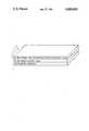
- FIGUREis a schematic showing of a detector made in accordance with the invention.
- layer 1is a III-V binary substrate.
- This substrateshould be in the form of a single crystal wafer of large area and low defect density; InSb is an ideal candidate, since it is available in diameters of 1.5 inches, and with etch pit density less than 100 per cm 2 .
- Buffer layer 2is a ZnCdTe compound, with the zinc concentration adjusted to lattice match the compound to infrared-absorbing layer 3.
- This layer 3is a II-VI compound with a narrow-bandgap infrared response.
- HgCdTe or HgZnTemay be chosen.
- substrate 1is prepared in the usual manner of preparing a semiconductor crystal slab, and the layers 2 and 3 are grown to the desired compositions and thickness and compositions by MBE.
- Typical compositions and thicknessesare as follows: HgCdTe, the buffer layer should be Zn 0 .045 Cd 0 .955 Te, and for HgZnTe, the buffer layer should be Zn 0 .2 Cd 0 .8 Te; each buffer layer is approximately 1 micron thick, and the infrared-absorbing layer is approximately 10 microns thick.
- substrate thicknessis not important, but is normally several mils.
- output leadsWhile no mention has been made of output leads for the device, it should be understood that such leads will be applied in the typical techniques used for semiconductor detectors. That is, the device may be masked and etched to delineate individual detector elements, and output leads may be bonded or deposited to such elements.
Landscapes
- Engineering & Computer Science (AREA)
- Physics & Mathematics (AREA)
- Condensed Matter Physics & Semiconductors (AREA)
- General Physics & Mathematics (AREA)
- Manufacturing & Machinery (AREA)
- Computer Hardware Design (AREA)
- Microelectronics & Electronic Packaging (AREA)
- Power Engineering (AREA)
- Chemical & Material Sciences (AREA)
- Materials Engineering (AREA)
- Light Receiving Elements (AREA)
Abstract
Description
The invention described herein may be manufactured, used, and licensed by the U.S. Government for governmental purposes without the payment of any royalties thereon.
This invention is in the field of semiconductor infrared detectors. In particular, it is concerned with those detectors wherein an optical absorbing layer is deposited on a substrate, and wherein the substrate is lattice matched to the layer. The desire has existed for a detector in the 3-5 or 8-14 micron spectral region using a narrow bandgap absorbing material such as HgCdTe or HgZnTe on a wider bandgap substrate. An ideal substrate will not only be lattice matched to the absorbing material, but will have negligable defect density. Unfortunately, no substrate material has been found which satisfies both these requirements. The currently available compound semiconductor materials which may be produced with low defect density are III-V compounds such as InSb or GaAs. Obviously, lattice matching to HgCdTe or HgZnTe is not possible with such compounds. In order to achieve lattice matching with HgCdTe or HgZnTe, one must use II-VI compounds such as ZnCdTe. The defect densities of such II-VI compounds, however, are three orders of magnitude higher than III-V compounds. The instant invention is a solution to this dilemma.
The invention is a unique infrared epitaxial detector and a method of making such a detector. The detector consists of a low defect-density III-V binary substrate covered with a buffer layer of II-VI ternary material preferably deposited by molecular beam epitaxy (MBE). A II-VI ternary narrow-bandpass infrared-absorbing layer is preferably deposited also by MBE. The substrate may be GaAs, but is preferably InSb, and the buffer layer is Znx Cd1-x Te of appropriate composition to lattice match the infrared absorbing layer.
The single drawing FIGURE is a schematic showing of a detector made in accordance with the invention.
The invention may be best understood when this description is taken in conjunction with the drawing. Referring now to the drawing, we see that layer 1 is a III-V binary substrate. This substrate should be in the form of a single crystal wafer of large area and low defect density; InSb is an ideal candidate, since it is available in diameters of 1.5 inches, and with etch pit density less than 100 per cm2.Buffer layer 2 is a ZnCdTe compound, with the zinc concentration adjusted to lattice match the compound to infrared-absorbinglayer 3. Thislayer 3 is a II-VI compound with a narrow-bandgap infrared response. Depending on whether one is interested in 3-5 or 8-14 micron portions of the spectrum, HgCdTe or HgZnTe may be chosen.
The method of the invention is straight forward: substrate 1 is prepared in the usual manner of preparing a semiconductor crystal slab, and thelayers
While no mention has been made of output leads for the device, it should be understood that such leads will be applied in the typical techniques used for semiconductor detectors. That is, the device may be masked and etched to delineate individual detector elements, and output leads may be bonded or deposited to such elements.
Claims (3)
1. An infrared detector structure including:
a III-V binary substrate chosen from the group consisting of GaAs and In-Sb;
a ternary II-VI buffer layer of a Znx Cd1-X Te compound atop said substrate;
a II-VI narrow-bandpass ternary infrared-absorbing layer chosen from the group consisting of HgCdTe and HgZnTe atop said buffer layer, wherein said buffer layer is lattice matched to said infrared absorbing layer.
2. The detector structure as set forth in claim 1 wherein the buffer layer is Zn0.045 Cd0.955 Te when HgCdTe is chosen as the infrared-absorbing layer.
3. The detector structure as set forth in claim 1 wherein the buffer layer is Zn0.2 Cd0.8 Te when HgZnTe is chosen as the infrared-absorbing layer.
Priority Applications (1)
| Application Number | Priority Date | Filing Date | Title |
|---|---|---|---|
| US06/783,702US4689650A (en) | 1985-10-03 | 1985-10-03 | Infrared epitaxial detector structure and method of making same |
Applications Claiming Priority (1)
| Application Number | Priority Date | Filing Date | Title |
|---|---|---|---|
| US06/783,702US4689650A (en) | 1985-10-03 | 1985-10-03 | Infrared epitaxial detector structure and method of making same |
Publications (1)
| Publication Number | Publication Date |
|---|---|
| US4689650Atrue US4689650A (en) | 1987-08-25 |
Family
ID=25130154
Family Applications (1)
| Application Number | Title | Priority Date | Filing Date |
|---|---|---|---|
| US06/783,702Expired - Fee RelatedUS4689650A (en) | 1985-10-03 | 1985-10-03 | Infrared epitaxial detector structure and method of making same |
Country Status (1)
| Country | Link |
|---|---|
| US (1) | US4689650A (en) |
Cited By (11)
| Publication number | Priority date | Publication date | Assignee | Title |
|---|---|---|---|---|
| US4793872A (en)* | 1986-03-07 | 1988-12-27 | Thomson-Csf | III-V Compound heteroepitaxial 3-D semiconductor structures utilizing superlattices |
| US4813049A (en)* | 1987-09-23 | 1989-03-14 | Massachusetts Institute Of Technology | Semimagnetic semiconductor laser |
| US4965649A (en)* | 1988-12-23 | 1990-10-23 | Ford Aerospace Corporation | Manufacture of monolithic infrared focal plane arrays |
| US5001532A (en)* | 1989-09-06 | 1991-03-19 | Rockwell International Corporation | Impurity band conduction detector having photoluminescent layer |
| US5432374A (en)* | 1993-02-08 | 1995-07-11 | Santa Barbara Research Center | Integrated IR and mm-wave detector |
| US5742089A (en)* | 1995-06-07 | 1998-04-21 | Hughes Electronics | Growth of low dislocation density HGCDTE detector structures |
| US5998235A (en)* | 1997-06-26 | 1999-12-07 | Lockheed Martin Corporation | Method of fabrication for mercury-based quaternary alloys of infrared sensitive materials |
| WO2007072021A1 (en)* | 2005-12-21 | 2007-06-28 | Durham Scientific Crystals Limited | Semiconductor device structure and method of manufacture thereof |
| US20080315342A1 (en)* | 2005-12-21 | 2008-12-25 | Durham Scientific Crystals Limited | Semiconductor Device with a Bulk Single Crystal on a Substrate |
| US20090053453A1 (en)* | 2005-12-21 | 2009-02-26 | Durham Scientific Crystals Limited | Semiconductor device and method of manufacture thereof |
| RU2396635C1 (en)* | 2009-08-11 | 2010-08-10 | Государственное образовательное учреждение высшего профессионального образования "Томский государственный университет" (ТГУ) | Infrared radiation sensitive structure and method of making said structure |
Citations (5)
| Publication number | Priority date | Publication date | Assignee | Title |
|---|---|---|---|---|
| US3218203A (en)* | 1961-10-09 | 1965-11-16 | Monsanto Co | Altering proportions in vapor deposition process to form a mixed crystal graded energy gap |
| JPS5224483A (en)* | 1975-08-20 | 1977-02-23 | Matsushita Electric Ind Co Ltd | Phptoconducting element |
| US4369372A (en)* | 1979-06-18 | 1983-01-18 | Canon Kabushiki Kaisha | Photo electro transducer device |
| JPS603165A (en)* | 1983-06-20 | 1985-01-09 | Matsushita Electric Ind Co Ltd | Light receiving element |
| US4553152A (en)* | 1982-11-06 | 1985-11-12 | Mitsubishi Denki Kabushiki Kaisha | Monolithic infrared ray charge transfer element |
- 1985
- 1985-10-03USUS06/783,702patent/US4689650A/ennot_activeExpired - Fee Related
Patent Citations (5)
| Publication number | Priority date | Publication date | Assignee | Title |
|---|---|---|---|---|
| US3218203A (en)* | 1961-10-09 | 1965-11-16 | Monsanto Co | Altering proportions in vapor deposition process to form a mixed crystal graded energy gap |
| JPS5224483A (en)* | 1975-08-20 | 1977-02-23 | Matsushita Electric Ind Co Ltd | Phptoconducting element |
| US4369372A (en)* | 1979-06-18 | 1983-01-18 | Canon Kabushiki Kaisha | Photo electro transducer device |
| US4553152A (en)* | 1982-11-06 | 1985-11-12 | Mitsubishi Denki Kabushiki Kaisha | Monolithic infrared ray charge transfer element |
| JPS603165A (en)* | 1983-06-20 | 1985-01-09 | Matsushita Electric Ind Co Ltd | Light receiving element |
Non-Patent Citations (2)
| Title |
|---|
| Levinstein, "Infrared Detectors", Physics Today, Nov. 1977, pp. 23-28. |
| Levinstein, Infrared Detectors , Physics Today , Nov. 1977, pp. 23 28.* |
Cited By (18)
| Publication number | Priority date | Publication date | Assignee | Title |
|---|---|---|---|---|
| US4793872A (en)* | 1986-03-07 | 1988-12-27 | Thomson-Csf | III-V Compound heteroepitaxial 3-D semiconductor structures utilizing superlattices |
| US4813049A (en)* | 1987-09-23 | 1989-03-14 | Massachusetts Institute Of Technology | Semimagnetic semiconductor laser |
| US4965649A (en)* | 1988-12-23 | 1990-10-23 | Ford Aerospace Corporation | Manufacture of monolithic infrared focal plane arrays |
| US5001532A (en)* | 1989-09-06 | 1991-03-19 | Rockwell International Corporation | Impurity band conduction detector having photoluminescent layer |
| US5432374A (en)* | 1993-02-08 | 1995-07-11 | Santa Barbara Research Center | Integrated IR and mm-wave detector |
| US5742089A (en)* | 1995-06-07 | 1998-04-21 | Hughes Electronics | Growth of low dislocation density HGCDTE detector structures |
| GB2326762B (en)* | 1997-06-26 | 2003-01-22 | Lockheed Corp | Defect reduction for interdiffused mercury cadmium telluride based infrared detector materials |
| US6208005B1 (en) | 1997-06-26 | 2001-03-27 | Lockheed Martin Corporation | Mercury-based quaternary alloys of infrared sensitive materials |
| US5998235A (en)* | 1997-06-26 | 1999-12-07 | Lockheed Martin Corporation | Method of fabrication for mercury-based quaternary alloys of infrared sensitive materials |
| WO2007072021A1 (en)* | 2005-12-21 | 2007-06-28 | Durham Scientific Crystals Limited | Semiconductor device structure and method of manufacture thereof |
| US20080315342A1 (en)* | 2005-12-21 | 2008-12-25 | Durham Scientific Crystals Limited | Semiconductor Device with a Bulk Single Crystal on a Substrate |
| US20090053453A1 (en)* | 2005-12-21 | 2009-02-26 | Durham Scientific Crystals Limited | Semiconductor device and method of manufacture thereof |
| US20100327277A1 (en)* | 2005-12-21 | 2010-12-30 | Durham Scientific Crystals Limited | Semiconductor device with a bulk single crystal on a substrate |
| US20110024877A1 (en)* | 2005-12-21 | 2011-02-03 | Durham Scientific Crystals Limited | Semiconductor device and method of manufacture thereof |
| US8093095B2 (en) | 2005-12-21 | 2012-01-10 | Kromek Limited | Semiconductor device with a bulk single crystal on a substrate |
| US8093671B2 (en) | 2005-12-21 | 2012-01-10 | Kromek Limited | Semiconductor device with a bulk single crystal on a substrate |
| US8968469B2 (en) | 2005-12-21 | 2015-03-03 | Kromek Limited | Semiconductor device and method of manufacture thereof |
| RU2396635C1 (en)* | 2009-08-11 | 2010-08-10 | Государственное образовательное учреждение высшего профессионального образования "Томский государственный университет" (ТГУ) | Infrared radiation sensitive structure and method of making said structure |
Similar Documents
| Publication | Publication Date | Title |
|---|---|---|
| US4689650A (en) | Infrared epitaxial detector structure and method of making same | |
| US5308980A (en) | Thermal mismatch accommodated infrared detector hybrid array | |
| Tsaur et al. | Molecular beam epitaxy of GaAs and AlGaAs on Si | |
| US5264699A (en) | Infrared detector hybrid array with improved thermal cycle reliability and method for making same | |
| Zogg et al. | Growth of high quality epitaxial PbSe onto Si using a (Ca, Ba) F2 buffer layer | |
| Bringans et al. | Formation of the interface between GaAs and Si: implications for GaAs‐on‐Si heteroepitaxy | |
| JPS6095981A (en) | Intrinsic semiconductor electro-optic device | |
| EP0069453A1 (en) | A process for forming semiconductor alloys having a desired bandgap | |
| US3961998A (en) | Vacuum deposition method for fabricating an epitaxial pbsnte rectifying metal semiconductor contact photodetector | |
| US6208005B1 (en) | Mercury-based quaternary alloys of infrared sensitive materials | |
| Sheldon et al. | Growth and patterning of GaAs/Ge single crystal layers on Si substrates by molecular beam epitaxy | |
| US5449927A (en) | Multilayer buffer structure including II-VI compounds on a silicon substrate | |
| US4328508A (en) | III-V Quaternary alloy photodiode | |
| George et al. | Absorption edge of tin disulfide single crystals | |
| Zogg et al. | Mis capacitors on BaF2/PbSe layers and epitaxial Si/BaF2/PBSE structures for IR detection | |
| CA2197295A1 (en) | Compounds and infrared devices including in1-xtlxq, where q is as1-ypy and 0 <= y <= 1 | |
| JPS57211238A (en) | Semiconductor device | |
| PESSA | Application of the ALE and MBE methods to the growth of layered Hg sub 1-x Cd sub x Te films(Interim Report) | |
| Bastard et al. | Optical characterization of III-V and II-VI semiconductor heterolayers | |
| US5512511A (en) | Process for growing HgCdTe base and contact layer in one operation | |
| Castro | Review of key trends in HgCdTe materials for IR focal plane arrays | |
| Ono et al. | Effects of local environment on localized vibrational modes of aluminum in Al x Ga 1− x As | |
| Bouley et al. | Epitaxial thin film IV-VI detectors: device performance and basic material properties | |
| JPH07161737A (en) | Growing method for hgcdte thin film | |
| JPS5661177A (en) | Preparation of semiconductor photodetector |
Legal Events
| Date | Code | Title | Description |
|---|---|---|---|
| AS | Assignment | Owner name:UNITED STATES OF AMERICA, THE, AS REPRESENTED BY T Free format text:ASSIGNMENT OF ASSIGNORS INTEREST.;ASSIGNOR:DINAN, JOHN H.;REEL/FRAME:004700/0886 Effective date:19850930 Owner name:UNITED STATES OF AMERICA, THE, AS REPRESENTED BY T Free format text:ASSIGNMENT OF ASSIGNORS INTEREST;ASSIGNOR:DINAN, JOHN H.;REEL/FRAME:004700/0886 Effective date:19850930 | |
| REMI | Maintenance fee reminder mailed | ||
| LAPS | Lapse for failure to pay maintenance fees | ||
| STCH | Information on status: patent discontinuation | Free format text:PATENT EXPIRED DUE TO NONPAYMENT OF MAINTENANCE FEES UNDER 37 CFR 1.362 | |
| FP | Lapsed due to failure to pay maintenance fee | Effective date:19910825 |