US4688897A - Liquid crystal device - Google Patents
Liquid crystal deviceDownload PDFInfo
- Publication number
- US4688897A US4688897AUS06/745,471US74547185AUS4688897AUS 4688897 AUS4688897 AUS 4688897AUS 74547185 AUS74547185 AUS 74547185AUS 4688897 AUS4688897 AUS 4688897A
- Authority
- US
- United States
- Prior art keywords
- grid
- liquid crystal
- polarizer
- light
- plane
- Prior art date
- Legal status (The legal status is an assumption and is not a legal conclusion. Google has not performed a legal analysis and makes no representation as to the accuracy of the status listed.)
- Expired - Lifetime
Links
- 239000004973liquid crystal related substanceSubstances0.000titleclaimsabstractdescription65
- 230000005684electric fieldEffects0.000claimsabstractdescription8
- 239000004988Nematic liquid crystalSubstances0.000claimsabstractdescription4
- 239000000463materialSubstances0.000claimsdescription36
- 239000004020conductorSubstances0.000claimsdescription35
- 239000000758substrateSubstances0.000claimsdescription25
- 230000010287polarizationEffects0.000claimsdescription17
- 230000005540biological transmissionEffects0.000claimsdescription13
- 238000005286illuminationMethods0.000claimsdescription7
- 239000013078crystalSubstances0.000claims2
- 239000007788liquidSubstances0.000claims1
- 239000011521glassSubstances0.000description10
- 230000008033biological extinctionEffects0.000description9
- 230000005855radiationEffects0.000description6
- 210000004027cellAnatomy0.000description3
- 230000003466anti-cipated effectEffects0.000description2
- 210000002858crystal cellAnatomy0.000description2
- 230000000694effectsEffects0.000description2
- 239000002184metalSubstances0.000description2
- 229910052751metalInorganic materials0.000description2
- 238000000034methodMethods0.000description2
- 238000000926separation methodMethods0.000description2
- 238000007493shaping processMethods0.000description2
- 238000010521absorption reactionMethods0.000description1
- 230000000593degrading effectEffects0.000description1
- 238000005516engineering processMethods0.000description1
- PCHJSUWPFVWCPO-UHFFFAOYSA-NgoldChemical compound[Au]PCHJSUWPFVWCPO-UHFFFAOYSA-N0.000description1
- 239000010931goldSubstances0.000description1
- 229910052737goldInorganic materials0.000description1
- 238000001093holographyMethods0.000description1
- 238000002329infrared spectrumMethods0.000description1
- 238000004519manufacturing processMethods0.000description1
- 239000011159matrix materialSubstances0.000description1
- 238000012986modificationMethods0.000description1
- 230000004048modificationEffects0.000description1
- 239000000382optic materialSubstances0.000description1
- 230000003287optical effectEffects0.000description1
- 229920002120photoresistant polymerPolymers0.000description1
- 238000012552reviewMethods0.000description1
- 238000004381surface treatmentMethods0.000description1
- 238000012360testing methodMethods0.000description1
- 238000001429visible spectrumMethods0.000description1
Images
Classifications
- G—PHYSICS
- G02—OPTICS
- G02F—OPTICAL DEVICES OR ARRANGEMENTS FOR THE CONTROL OF LIGHT BY MODIFICATION OF THE OPTICAL PROPERTIES OF THE MEDIA OF THE ELEMENTS INVOLVED THEREIN; NON-LINEAR OPTICS; FREQUENCY-CHANGING OF LIGHT; OPTICAL LOGIC ELEMENTS; OPTICAL ANALOGUE/DIGITAL CONVERTERS
- G02F1/00—Devices or arrangements for the control of the intensity, colour, phase, polarisation or direction of light arriving from an independent light source, e.g. switching, gating or modulating; Non-linear optics
- G02F1/01—Devices or arrangements for the control of the intensity, colour, phase, polarisation or direction of light arriving from an independent light source, e.g. switching, gating or modulating; Non-linear optics for the control of the intensity, phase, polarisation or colour
- G02F1/13—Devices or arrangements for the control of the intensity, colour, phase, polarisation or direction of light arriving from an independent light source, e.g. switching, gating or modulating; Non-linear optics for the control of the intensity, phase, polarisation or colour based on liquid crystals, e.g. single liquid crystal display cells
- G02F1/133—Constructional arrangements; Operation of liquid crystal cells; Circuit arrangements
- G02F1/1333—Constructional arrangements; Manufacturing methods
- G02F1/1335—Structural association of cells with optical devices, e.g. polarisers or reflectors
- G02F1/133528—Polarisers
- G02F1/133536—Reflective polarizers
- G—PHYSICS
- G02—OPTICS
- G02B—OPTICAL ELEMENTS, SYSTEMS OR APPARATUS
- G02B5/00—Optical elements other than lenses
- G02B5/30—Polarising elements
- G02B5/3025—Polarisers, i.e. arrangements capable of producing a definite output polarisation state from an unpolarised input state
- G02B5/3058—Polarisers, i.e. arrangements capable of producing a definite output polarisation state from an unpolarised input state comprising electrically conductive elements, e.g. wire grids, conductive particles
- G—PHYSICS
- G02—OPTICS
- G02F—OPTICAL DEVICES OR ARRANGEMENTS FOR THE CONTROL OF LIGHT BY MODIFICATION OF THE OPTICAL PROPERTIES OF THE MEDIA OF THE ELEMENTS INVOLVED THEREIN; NON-LINEAR OPTICS; FREQUENCY-CHANGING OF LIGHT; OPTICAL LOGIC ELEMENTS; OPTICAL ANALOGUE/DIGITAL CONVERTERS
- G02F1/00—Devices or arrangements for the control of the intensity, colour, phase, polarisation or direction of light arriving from an independent light source, e.g. switching, gating or modulating; Non-linear optics
- G02F1/01—Devices or arrangements for the control of the intensity, colour, phase, polarisation or direction of light arriving from an independent light source, e.g. switching, gating or modulating; Non-linear optics for the control of the intensity, phase, polarisation or colour
- G02F1/13—Devices or arrangements for the control of the intensity, colour, phase, polarisation or direction of light arriving from an independent light source, e.g. switching, gating or modulating; Non-linear optics for the control of the intensity, phase, polarisation or colour based on liquid crystals, e.g. single liquid crystal display cells
- G02F1/133—Constructional arrangements; Operation of liquid crystal cells; Circuit arrangements
- G02F1/1333—Constructional arrangements; Manufacturing methods
- G02F1/1335—Structural association of cells with optical devices, e.g. polarisers or reflectors
- G02F1/133553—Reflecting elements
- G—PHYSICS
- G02—OPTICS
- G02F—OPTICAL DEVICES OR ARRANGEMENTS FOR THE CONTROL OF LIGHT BY MODIFICATION OF THE OPTICAL PROPERTIES OF THE MEDIA OF THE ELEMENTS INVOLVED THEREIN; NON-LINEAR OPTICS; FREQUENCY-CHANGING OF LIGHT; OPTICAL LOGIC ELEMENTS; OPTICAL ANALOGUE/DIGITAL CONVERTERS
- G02F1/00—Devices or arrangements for the control of the intensity, colour, phase, polarisation or direction of light arriving from an independent light source, e.g. switching, gating or modulating; Non-linear optics
- G02F1/01—Devices or arrangements for the control of the intensity, colour, phase, polarisation or direction of light arriving from an independent light source, e.g. switching, gating or modulating; Non-linear optics for the control of the intensity, phase, polarisation or colour
- G02F1/13—Devices or arrangements for the control of the intensity, colour, phase, polarisation or direction of light arriving from an independent light source, e.g. switching, gating or modulating; Non-linear optics for the control of the intensity, phase, polarisation or colour based on liquid crystals, e.g. single liquid crystal display cells
- G02F1/133—Constructional arrangements; Operation of liquid crystal cells; Circuit arrangements
- G02F1/1333—Constructional arrangements; Manufacturing methods
- G02F1/1343—Electrodes
- G02F1/13439—Electrodes characterised by their electrical, optical, physical properties; materials therefor; method of making
- G—PHYSICS
- G02—OPTICS
- G02F—OPTICAL DEVICES OR ARRANGEMENTS FOR THE CONTROL OF LIGHT BY MODIFICATION OF THE OPTICAL PROPERTIES OF THE MEDIA OF THE ELEMENTS INVOLVED THEREIN; NON-LINEAR OPTICS; FREQUENCY-CHANGING OF LIGHT; OPTICAL LOGIC ELEMENTS; OPTICAL ANALOGUE/DIGITAL CONVERTERS
- G02F1/00—Devices or arrangements for the control of the intensity, colour, phase, polarisation or direction of light arriving from an independent light source, e.g. switching, gating or modulating; Non-linear optics
- G02F1/01—Devices or arrangements for the control of the intensity, colour, phase, polarisation or direction of light arriving from an independent light source, e.g. switching, gating or modulating; Non-linear optics for the control of the intensity, phase, polarisation or colour
- G02F1/13—Devices or arrangements for the control of the intensity, colour, phase, polarisation or direction of light arriving from an independent light source, e.g. switching, gating or modulating; Non-linear optics for the control of the intensity, phase, polarisation or colour based on liquid crystals, e.g. single liquid crystal display cells
- G02F1/133—Constructional arrangements; Operation of liquid crystal cells; Circuit arrangements
- G02F1/1333—Constructional arrangements; Manufacturing methods
- G02F1/1335—Structural association of cells with optical devices, e.g. polarisers or reflectors
- G02F1/133553—Reflecting elements
- G02F1/133555—Transflectors
Definitions
- This inventionrelates to electro-optic devices and, more particularly, to liquid crystal displays.
- liquid crystal displayshave been devised since the properties of liquid crystal materials were found to be useful in display technologies.
- One of the more popular types of liquid crystal displaysutilizes the properties of nematic-phase liquid crystal materials to form a twisted nematic display operating in the reflective mode.
- a cellis constructed in which the nematic material is sandwiched between front and rear transparent substrates which have received one or more forms of surface treatment and which are oriented in a particular relationship to one another so as to produce an optical media which in its relaxed state rotates the plane of polarization of light passing through it by ninety degrees.
- Such an arrangementgenerally utilizes a first absorbing type polarizer which restricts the light entering and leaving the front of the cell to that having a particular plane of polarization.
- a second absorbing polarizerhaving its plane of transmission rotated ninety degrees with respect to the first polarizer is positioned behind the liquid crystal cell, and a mirror is positioned behind the second polarizer.
- the light passing through the first polarizer and the front substratehas its polarization plane twisted by the liquid crystal material so that the light exiting the cell passes through the second polarizer, is reflected by the mirror, and travels back through the same path to appear as a bright area on the display.
- the two substratesare each provided with transparent electrodes.
- a voltage placed across these electrodesprovides an electric field which causes the liquid crystal molecules to rotate, and thus untwist.
- light passing through the first polarizer and into the liquid crystal materialdoes not pass through the second polarizer, since its polarization plane is no longer twisted into alignment with this polarizer. Instead, the light is absorbed by the second polarizer, creating a dark area on the display.
- a wire grid polarizerreplaces the second transparent electrode, the second polarizer, and the mirror of a conventional liquid crystal display.
- the gridis formed by closely spaced parallel electrical conductors. By connecting the thin conductors of the grid together, the grid may be made to act as an electrode. By properly spacing the grid conductors, the grid may be made to act as a polarizer which, rather than absorbing cross-polarized light, transmits that light. Light polarized parallel to the grid conductors is reflected. By reflecting light of one polarization while transmitting light of another polarization, the electrode acts as both a polarizer and a mirror, substantially increasing the contrast over previous devices using a separate polarizer and mirror.
- the complexity of the displayis reduced substantially. Since the wire grid polarizer is in intimate contact with the liquid crystal material, parallax is also reduced substantially, which acts to increase the resolution of the display.
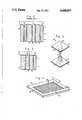
- FIG. 1is a cross sectional view of a conventional twisted nematic-phase liquid crystal display of the prior art
- FIG. 2is a perspective view of a portion of a conventional twisted nematic-phase liquid crystal display of the prior art
- FIG. 3is a cross sectional view of the improved twisted nematic-phase liquid crystal display of the present invention.
- FIG. 4is a perspective view illustrating a wire grid polarizer which may be utilized with the present invention.
- FIG. 1illustrates in cross section a conventional reflective-type liquid crystal display 10 of the twisted nematic-phase variety.
- the displayincludes a liquid crystal material 11 positioned between a first glass plate 12 and a second glass plate 13.
- Each of these plateshas one or more transparent electrodes deposited on its surface adjacent the liquid crystal material 11.
- an electrode 15is deposited on the surface of the glass plate 13 and an electrode 16 is deposited on the surface of the glass plate 12.
- a first polarizer 18is positioned between a source of incident light and the glass plate 12 and forms the front of the display 10.
- a second polarizer 19is positioned behind the second glass plate 13, and a mirror 20 is positioned behind the second polarizer 19.
- a liquid crystal material with a positive dielectric anisotropy and a high impedanceis generally used.
- the molecules of the liquid crystal material adjacent the glass surfacesare caused to align parallel to the surfaces of the plates and in a preferred direction.
- the plates 12 and 13are oriented with respect to each other so that the preferred molecular alignment direction of these plates, denoted by arrows 14 and 17 respectively, are orthogonal.
- This orientationcauses the twisted effect in the liquid crystal material, as illustrated by the twisted plane 11 in FIG. 2.
- the twisted configurationinduces a ninety degree twist in the polarization of the light passing through the liquid crystal material in its relaxed state.
- Such an effectis described in U.S. Pat. No. 3,731,986, entitled Display Devices Using Liquid Crystal Light Modulation, issued to James L. Fergason, on May 8, 1973.
- First polarizer 18is oriented with respect to plate 12 so that polarized light emerging from the polarizer 18 will pass through the liquid crystal molecules.
- second polarizer 19is oriented with its transmission plane at ninety degrees to that of polarizer 18, whereby light proceeding through and having its polarization plane rotated ninety degrees by the twisted molecules will pass through the second polarizer 19.
- the operation of the device 10 with the liquid crystal molecules in their relaxed (twisted) stateis as follows.
- Light entering from the right in FIG. 1passes through the polarizer 18.
- the polarized light emerging therefrompasses through the plate 12 and the transparent electrode 16, and has its plane of polarization rotated ninety degrees by the liquid crystal molecules.
- liquid crystal displayAnother problem associated with conventional liquid crystal displays is the low contrast obtainable between light and dark areas at low ambient light levels. For example, the liquid crystal display often receives light at an angle, where the amount which is transmitted by the polarizers compared to that absorbed is quite low. This results in a lowering of the contrast of the display.
- a liquid crystal display 22 constructed in accordance with the teachings of the present inventionis shown in FIG. 3.
- the polarizer 19 and the mirror 20 of the display 10are omitted; and a metal grid 24 is provided in place of the electrode 15 on the surface of the glass plate 13 which lies adjacent the liquid crystal material 11.
- the grid 24acts as an electrode, a polarizer and a mirror in the present invention.
- the liquid crystal material 11lies in a twisted configuration between the planar glass plates 12 and 13 and the transparent electrode 16 is provided on the surface of the plate 12 adjacent the liquid crystal material 11.
- electrode 16could reside on the other surface of substrate 12 if it has a low enough electrical impedance.
- FIG. 4illustrates a typical configuration of a grid 24 of individual conductors 26 placed upon one surface of the plate 13. The ends of each of the conductors 26 are joined together by conductive material 28 so that all points on the grid 24 can be placed at the same potential and act as the rear electrode 24 for the display 22.
- Wire gridshave been used for many years for polarizing various electromagnetic waves.
- a grid of suitably spaced fine metallic conductorsreflects an electromagnetic wave when the wave is polarized in the direction of the conductors.
- a wave polarized perpendicular to the conductors of the gridpasses through the grid with little transmission loss.
- the effectiveness of the grid as a polarizerdepends on the width and spacing of the conductors in relation to the wavelength of the incident radiation, as described below.
- the present inventionutilizes a grid comprising closely spaced parallel lines of conductive material (hereinafter referred to as a wire grid even though the conductive lines may not actually be wires) in the display 22 to replace the conventional second polarizer 19 used in the prior art display 10.
- the transmission plane of the grid 24(the plane at which light polarized parallel thereto is transmitted through the grid) may be oriented parallel to the tranmission plane of the first polarizer 18, so that light having its polarization twisted by the relaxed twisted liquid crystal molecules does not pass through the grid 24 but is instead reflected by it. The reflected light travels back through the display and appears to the viewer as a bright area.
- the untwisted moleculesUpon application of an electric field, the untwisted molecules permit light to pass through the display without rotation of the polarization plane. This light passes through the grid 24 and, since no mirror is present, the light is not reflected back to the viewer, who will thus perceive a dark image in the area subjected to the electric field.
- the operation of the display 22is substantially identical to the operation of the display 10, with, however, several distinct advantages, as discussed below. It should be noted that the transmission plane of the grid 24 can be oriented at ninety degrees to the transmission plane of the first polarizer 18. In such instance, the displayed image will be reversed. That is, the display will be normally dark, with images appearing as bright areas.
- a voltageis applied between the transparent electrode 16 and the wire grid 24.
- the conductive lines 26, connected together by the end connectors 28thus act in place of the rear elecrode 15 used in the prior art display 10.
- the polarizer 18 and 19 employed in the prior art display 10either absorb or transmit light, depending upon the polarization of that light.
- the grid 24either reflects or transmits light as a function of its polarization. Further, it will be appreciated that the reflection from grid 24 takes place directly at the interface between the liquid crystal material 11 and the inner surface of the plate 13. This is unlike the prior art display 10 where light travels through the plate 13, and the polarizer 19 before it is reflected.
- the reflective characteristic of the grid 24 and its close proximity to the active electro-optic material 11combine both to enhance the contrast of the display and to substantially reduce parallax. This reduction in parallax greatly improves the resolution of the display under off-normal viewing conditions.
- the dimensions of the grid 24must be chosen to provide suitable transmission and reflection characteristics at the wavelength of the incident light.
- One measure of the effectiveness of a wire grid in this applicationis referred to as the extinction ratio of the grid.
- the transmission extinction ratio of a gridis the ratio of the amount of light transmitted through the grid from a light source polarized perpendicular to the grid lines to the amount of light transmitted through the grid when that same light source is polarized parallel to the grid lines.
- the reflection extinction ratiois defined in a similar fashion.
- the grating period of the gridshould be one-tenth (or less) of the wavelength of the incident radiation. Further, the coverage of the grid surface by the grid lines should be in the range of 40 to 80 percent.
- the grating period for the gridis the sum of the width of a grid line (shown as the dimension a in FIG. 4) and the width of the space between adjacent lines. This sum is shown as the dimension d in FIG. 4. The coverage of the grid surface by the grid lines is expressed by the ratio a/d.
- the grid 24having a grating period on the order of 0.05 microns, while for incident light in the infrared spectrum, a grating period on the order of 0.3 microns is adequate.
- grids 24In the fabrication of grids 24, laser holography has been used to expose photoresist grating patterns which are sputter etched into gold metal films on the surface of transparent substrates. Using this technique, grids have been fabricated with a grating period of 0.28 microns and a 60 to 70 percent coverage of the grid surface by the grid lines.
- the extinction ratios of the above fabricated gridswere measured using both infrared and visible light. With infrared incident radiation at a wavelength of 3.39 microns, the transmission extinction ratio of the grid was on the order of six thousand. With visible incident radiation at a wavelength of 0.633 microns, reflection and transmission extinction ratios on the order of 30 and 45, respectively, were measured. Tests conducted with off-normal incident radiation at angles up to forty-five degrees indicated that extinction ratios did not degrade significantly from those measured with incident radiation normal to the plane of the grid. It is anticipated that grids having grating periods substantially smaller than those described above will be fabricated in the near future.
- each grid linemight be fabricated as a "dotted line" comprising individual conductive segments separated from each other.
- Yet another advantage provided by the use of the grid 24 in place of the rear polarizer 19 and mirror 20 of the prior artis that it enables the use of back illumination without degrading the contrast of the display. Back illumination is desirable in situations where ambient front illumination is inadequate for viewing the display.
- the partially silvered mirrorreduces the contrast of the display when used with either front or rear illumination.
- the display 22 of the present inventionmay be backlit simply by providing a source of light behind the rear plate 13. Accordingly, contrast remains high in this configuration regardless of whether front or rear illumination is provided.
Landscapes
- Physics & Mathematics (AREA)
- Nonlinear Science (AREA)
- General Physics & Mathematics (AREA)
- Optics & Photonics (AREA)
- Mathematical Physics (AREA)
- Chemical & Material Sciences (AREA)
- Crystallography & Structural Chemistry (AREA)
- Liquid Crystal (AREA)
Abstract
Description
Claims (15)
Priority Applications (1)
| Application Number | Priority Date | Filing Date | Title |
|---|---|---|---|
| US06/745,471US4688897A (en) | 1985-06-17 | 1985-06-17 | Liquid crystal device |
Applications Claiming Priority (1)
| Application Number | Priority Date | Filing Date | Title |
|---|---|---|---|
| US06/745,471US4688897A (en) | 1985-06-17 | 1985-06-17 | Liquid crystal device |
Publications (1)
| Publication Number | Publication Date |
|---|---|
| US4688897Atrue US4688897A (en) | 1987-08-25 |
Family
ID=24996834
Family Applications (1)
| Application Number | Title | Priority Date | Filing Date |
|---|---|---|---|
| US06/745,471Expired - LifetimeUS4688897A (en) | 1985-06-17 | 1985-06-17 | Liquid crystal device |
Country Status (1)
| Country | Link |
|---|---|
| US (1) | US4688897A (en) |
Cited By (70)
| Publication number | Priority date | Publication date | Assignee | Title |
|---|---|---|---|---|
| US4998338A (en)* | 1988-11-05 | 1991-03-12 | Sms Schloemann-Siemag Aktiengesellschaft | Method and arrangement for manufacturing hot-rolled steel strip |
| WO1994011776A1 (en)* | 1992-11-09 | 1994-05-26 | Honeywell Inc. | Backlit display |
| US5416324A (en)* | 1993-06-11 | 1995-05-16 | Chun; Cornell S. L. | Optical imaging device with integrated polarizer |
| EP0871923A1 (en)* | 1995-06-26 | 1998-10-21 | Minnesota Mining And Manufacturing Company | Transflective displays with reflective polarizing transflector |
| US5986730A (en)* | 1998-12-01 | 1999-11-16 | Moxtek | Dual mode reflective/transmissive liquid crystal display apparatus |
| US5999239A (en)* | 1995-04-07 | 1999-12-07 | Honeywell Inc. | Method for making a polarization-sensitive optical element |
| US6081376A (en)* | 1998-07-16 | 2000-06-27 | Moxtek | Reflective optical polarizer device with controlled light distribution and liquid crystal display incorporating the same |
| US6080467A (en)* | 1995-06-26 | 2000-06-27 | 3M Innovative Properties Company | High efficiency optical devices |
| US6108131A (en)* | 1998-05-14 | 2000-08-22 | Moxtek | Polarizer apparatus for producing a generally polarized beam of light |
| US6122103A (en)* | 1999-06-22 | 2000-09-19 | Moxtech | Broadband wire grid polarizer for the visible spectrum |
| US6185039B1 (en) | 1997-12-06 | 2001-02-06 | 3M Innovative Properties Co. | Infrared selective reflective polarizing element |
| US6208463B1 (en) | 1998-05-14 | 2001-03-27 | Moxtek | Polarizer apparatus for producing a generally polarized beam of light |
| US6234634B1 (en) | 1999-07-28 | 2001-05-22 | Moxtek | Image projection system with a polarizing beam splitter |
| US6243199B1 (en) | 1999-09-07 | 2001-06-05 | Moxtek | Broad band wire grid polarizing beam splitter for use in the visible wavelength region |
| US6288840B1 (en) | 1999-06-22 | 2001-09-11 | Moxtek | Imbedded wire grid polarizer for the visible spectrum |
| WO2001027962A3 (en)* | 1999-10-13 | 2002-01-10 | Fusion Lighting Inc | Lamp apparatus and method for effectively utilizing light from an aperture lamp |
| US20020044351A1 (en)* | 2000-08-15 | 2002-04-18 | Reflexite Corporation | Light polarizer |
| US6447120B2 (en) | 1999-07-28 | 2002-09-10 | Moxtex | Image projection system with a polarizing beam splitter |
| US20020158414A1 (en)* | 2001-04-27 | 2002-10-31 | Chih-Hao Yiu | Dart board display device |
| US20030112510A1 (en)* | 2001-12-13 | 2003-06-19 | Florence James M. | Polarized light beam splitter assembly including embedded wire grid polarizer |
| US6592224B2 (en)* | 2000-01-28 | 2003-07-15 | Seiko Epson Corporation | Optical reflection polarizer and projector comprising the same |
| US20030210369A1 (en)* | 2002-05-07 | 2003-11-13 | Shin-Tson Wu | Reflective and transflective liquid crystal display using a wire grid polarizer |
| US6666556B2 (en) | 1999-07-28 | 2003-12-23 | Moxtek, Inc | Image projection system with a polarizing beam splitter |
| US6707595B2 (en) | 2002-02-26 | 2004-03-16 | Eastman Kodak Company | Micro-mechanical polarization-based modulator |
| US20040125449A1 (en)* | 2002-12-30 | 2004-07-01 | Sales Tasso R. | Grid polarizer with suppressed reflectivity |
| US6785050B2 (en) | 2002-05-09 | 2004-08-31 | Moxtek, Inc. | Corrosion resistant wire-grid polarizer and method of fabrication |
| US20040169791A1 (en)* | 2000-08-15 | 2004-09-02 | Reflexite Corporation | Light polarizer |
| US20050140839A1 (en)* | 2003-12-30 | 2005-06-30 | Hyung Ki Hong | Liquid crystal display device |
| US20050277063A1 (en)* | 2004-04-15 | 2005-12-15 | Wang Jian J | Optical films and methods of making the same |
| US20050275944A1 (en)* | 2004-06-11 | 2005-12-15 | Wang Jian J | Optical films and methods of making the same |
| US20060001969A1 (en)* | 2004-07-02 | 2006-01-05 | Nanoopto Corporation | Gratings, related optical devices and systems, and methods of making such gratings |
| US20060061519A1 (en)* | 2004-09-17 | 2006-03-23 | Fisher Arthur D | Microdisplay |
| US20060061862A1 (en)* | 2004-09-23 | 2006-03-23 | Eastman Kodak Company | Low fill factor wire grid polarizer and method of use |
| US20060119937A1 (en)* | 2004-12-06 | 2006-06-08 | Moxtek, Inc. | Multilayer wire-grid polarizer |
| US20060127830A1 (en)* | 2004-12-15 | 2006-06-15 | Xuegong Deng | Structures for polarization and beam control |
| US20060127829A1 (en)* | 2004-12-15 | 2006-06-15 | Xuegong Deng | Structures for polarization and beam control |
| US20070008775A1 (en)* | 2005-07-11 | 2007-01-11 | Nicola Telecco | Memory architecture with enhanced over-erase tolerant control gate scheme |
| JP2007003787A (en)* | 2005-06-23 | 2007-01-11 | Seiko Epson Corp | Method for manufacturing liquid crystal device, liquid crystal device, and projector |
| US7184115B2 (en) | 2002-01-07 | 2007-02-27 | Moxtek, Inc. | Display apparatus with two polarization compensators |
| US7221420B2 (en) | 2002-01-07 | 2007-05-22 | Sony Corporation | Display with a wire grid polarizing beamsplitter |
| US20070139771A1 (en)* | 2005-12-15 | 2007-06-21 | Jian Wang | Optical retarders and methods of making the same |
| US20070165308A1 (en)* | 2005-12-15 | 2007-07-19 | Jian Wang | Optical retarders and methods of making the same |
| US20070217008A1 (en)* | 2006-03-17 | 2007-09-20 | Wang Jian J | Polarizer films and methods of making the same |
| US20070281143A1 (en)* | 2006-06-05 | 2007-12-06 | Aylward Peter T | Diffusely-reflecting element and method of making |
| US7306338B2 (en) | 1999-07-28 | 2007-12-11 | Moxtek, Inc | Image projection system with a polarizing beam splitter |
| US20080038467A1 (en)* | 2006-08-11 | 2008-02-14 | Eastman Kodak Company | Nanostructured pattern method of manufacture |
| US20080043329A1 (en)* | 2004-09-03 | 2008-02-21 | Koninklijke Philips Electronics, N.V. | Display Device With Birefringent Substrate |
| US7375887B2 (en) | 2001-03-27 | 2008-05-20 | Moxtek, Inc. | Method and apparatus for correcting a visible light beam using a wire-grid polarizer |
| US20080128927A1 (en)* | 2002-10-24 | 2008-06-05 | 3M Innovative Properties Company | Methods of making high gain optical devices having a continuous and dispersive phase |
| CN100449373C (en)* | 2005-10-04 | 2009-01-07 | 乐金显示有限公司 | Liquid crystal display panel and manufacturing method thereof |
| US7630133B2 (en) | 2004-12-06 | 2009-12-08 | Moxtek, Inc. | Inorganic, dielectric, grid polarizer and non-zero order diffraction grating |
| US20100128347A1 (en)* | 2008-11-19 | 2010-05-27 | Herb He Huang | Polarizing cube and method of fabricating the same |
| US7789515B2 (en) | 2007-05-17 | 2010-09-07 | Moxtek, Inc. | Projection device with a folded optical path and wire-grid polarizer |
| US7800823B2 (en) | 2004-12-06 | 2010-09-21 | Moxtek, Inc. | Polarization device to polarize and further control light |
| US20110025957A1 (en)* | 2009-08-03 | 2011-02-03 | Jiangsu Lexvu Electronics Co., Ltd. | Liquid crystal on silicon imager |
| DE102006023437B4 (en)* | 2005-05-18 | 2011-03-31 | Cheil Industries Inc., Gumi | Backlight and liquid crystal display device |
| US7961393B2 (en) | 2004-12-06 | 2011-06-14 | Moxtek, Inc. | Selectively absorptive wire-grid polarizer |
| US20110168999A1 (en)* | 2010-01-13 | 2011-07-14 | Samsung Electronics Co., Ltd. | Semiconductor wire grid, display apparatus having the same, and method of manufacturing the display apparatus |
| US20110222002A1 (en)* | 2010-03-10 | 2011-09-15 | Samsung Electronics Co., Ltd. | Liquid crystal display |
| US20120162582A1 (en)* | 2010-12-28 | 2012-06-28 | Jong Hoon Woo | Liquid crystal display device |
| US8248696B2 (en) | 2009-06-25 | 2012-08-21 | Moxtek, Inc. | Nano fractal diffuser |
| US8611007B2 (en) | 2010-09-21 | 2013-12-17 | Moxtek, Inc. | Fine pitch wire grid polarizer |
| US8755113B2 (en) | 2006-08-31 | 2014-06-17 | Moxtek, Inc. | Durable, inorganic, absorptive, ultra-violet, grid polarizer |
| US8873144B2 (en) | 2011-05-17 | 2014-10-28 | Moxtek, Inc. | Wire grid polarizer with multiple functionality sections |
| US8913321B2 (en) | 2010-09-21 | 2014-12-16 | Moxtek, Inc. | Fine pitch grid polarizer |
| US8913320B2 (en) | 2011-05-17 | 2014-12-16 | Moxtek, Inc. | Wire grid polarizer with bordered sections |
| US8922890B2 (en) | 2012-03-21 | 2014-12-30 | Moxtek, Inc. | Polarizer edge rib modification |
| US9348076B2 (en) | 2013-10-24 | 2016-05-24 | Moxtek, Inc. | Polarizer with variable inter-wire distance |
| CN107526205A (en)* | 2016-06-17 | 2017-12-29 | 三星显示有限公司 | Liquid crystal display device |
| CN111316160A (en)* | 2017-11-27 | 2020-06-19 | 金泰克斯公司 | Switchable polarization display |
Citations (4)
| Publication number | Priority date | Publication date | Assignee | Title |
|---|---|---|---|---|
| US3731986A (en)* | 1971-04-22 | 1973-05-08 | Int Liquid Xtal Co | Display devices utilizing liquid crystal light modulation |
| US4228574A (en)* | 1979-05-29 | 1980-10-21 | Texas Instruments Incorporated | Automated liquid crystal display process |
| US4256787A (en)* | 1978-05-03 | 1981-03-17 | Massachusetts Institute Of Technology | Orientation of ordered liquids and their use in devices |
| US4537471A (en)* | 1983-12-23 | 1985-08-27 | Hughes Aircraft Company | Liquid crystal pixel driver circuit and matrix display |
- 1985
- 1985-06-17USUS06/745,471patent/US4688897A/ennot_activeExpired - Lifetime
Patent Citations (4)
| Publication number | Priority date | Publication date | Assignee | Title |
|---|---|---|---|---|
| US3731986A (en)* | 1971-04-22 | 1973-05-08 | Int Liquid Xtal Co | Display devices utilizing liquid crystal light modulation |
| US4256787A (en)* | 1978-05-03 | 1981-03-17 | Massachusetts Institute Of Technology | Orientation of ordered liquids and their use in devices |
| US4228574A (en)* | 1979-05-29 | 1980-10-21 | Texas Instruments Incorporated | Automated liquid crystal display process |
| US4537471A (en)* | 1983-12-23 | 1985-08-27 | Hughes Aircraft Company | Liquid crystal pixel driver circuit and matrix display |
Non-Patent Citations (2)
| Title |
|---|
| Tove Larsen, "A Survey of the Theory of Wire Grids", IRE Transactions on Microwave Theory and Techniques, 1962, pp. 191-201. |
| Tove Larsen, A Survey of the Theory of Wire Grids , IRE Transactions on Microwave Theory and Techniques, 1962, pp. 191 201.* |
Cited By (120)
| Publication number | Priority date | Publication date | Assignee | Title |
|---|---|---|---|---|
| US4998338A (en)* | 1988-11-05 | 1991-03-12 | Sms Schloemann-Siemag Aktiengesellschaft | Method and arrangement for manufacturing hot-rolled steel strip |
| WO1994011776A1 (en)* | 1992-11-09 | 1994-05-26 | Honeywell Inc. | Backlit display |
| US5416324A (en)* | 1993-06-11 | 1995-05-16 | Chun; Cornell S. L. | Optical imaging device with integrated polarizer |
| US20010008464A1 (en)* | 1995-03-10 | 2001-07-19 | 3M Innovative Properties Company | Transflective displays with reflective polarizing trasflector |
| US6888675B2 (en) | 1995-03-10 | 2005-05-03 | 3M Innovative Properties Company | Transflective displays with reflective polarizing transflector |
| EP1258749A3 (en)* | 1995-04-07 | 2004-01-28 | Honeywell Inc. | High efficiency polarized display |
| US5999239A (en)* | 1995-04-07 | 1999-12-07 | Honeywell Inc. | Method for making a polarization-sensitive optical element |
| EP1258748A3 (en)* | 1995-04-07 | 2004-01-28 | Honeywell Inc. | High efficiency polarized display |
| US6310671B1 (en) | 1995-04-07 | 2001-10-30 | Honeywell, Inc. | Polarization sensitive scattering element |
| US6124971A (en)* | 1995-06-26 | 2000-09-26 | 3M Innovative Properties Company | Transflective displays with reflective polarizing transflector |
| US7833593B2 (en) | 1995-06-26 | 2010-11-16 | 3M Innovative Properties Company | High efficiency optical devices |
| EP0871923A1 (en)* | 1995-06-26 | 1998-10-21 | Minnesota Mining And Manufacturing Company | Transflective displays with reflective polarizing transflector |
| US20040175552A1 (en)* | 1995-06-26 | 2004-09-09 | Ouderkirk Andrew J. | High efficiency optical devices |
| US6210785B1 (en) | 1995-06-26 | 2001-04-03 | 3M Innovative Properties Company | High efficiency optical devices |
| US20050260384A1 (en)* | 1995-06-26 | 2005-11-24 | 3M Innovative Properties Company | High efficiency optical devices |
| US7147903B2 (en) | 1995-06-26 | 2006-12-12 | 3M Innovative Properties Company | High efficiency optical devices |
| US6262842B1 (en) | 1995-06-26 | 2001-07-17 | 3M Innovative Properties Company | Transflective displays with reflective polarizing transflector |
| US6924014B2 (en) | 1995-06-26 | 2005-08-02 | 3Minnovative Properties Company | High efficiency optical devices |
| US6080467A (en)* | 1995-06-26 | 2000-06-27 | 3M Innovative Properties Company | High efficiency optical devices |
| US20070092728A1 (en)* | 1995-06-26 | 2007-04-26 | 3M Innovative Properties Company | High efficiency optical devices |
| US6641883B2 (en) | 1995-06-26 | 2003-11-04 | 3M Innovative Properties Company | High efficiency optical devices |
| US20070122641A1 (en)* | 1995-06-26 | 2007-05-31 | 3M Innovative Properties Company | High Efficiency Optical Devices |
| US6185039B1 (en) | 1997-12-06 | 2001-02-06 | 3M Innovative Properties Co. | Infrared selective reflective polarizing element |
| US6452724B1 (en) | 1998-05-14 | 2002-09-17 | Moxtek | Polarizer apparatus for producing a generally polarized beam of light |
| US6710921B2 (en) | 1998-05-14 | 2004-03-23 | Moxtek | Polarizer apparatus for producing a generally polarized beam of light |
| US6108131A (en)* | 1998-05-14 | 2000-08-22 | Moxtek | Polarizer apparatus for producing a generally polarized beam of light |
| US6208463B1 (en) | 1998-05-14 | 2001-03-27 | Moxtek | Polarizer apparatus for producing a generally polarized beam of light |
| US6081376A (en)* | 1998-07-16 | 2000-06-27 | Moxtek | Reflective optical polarizer device with controlled light distribution and liquid crystal display incorporating the same |
| EP1095308A4 (en)* | 1998-07-16 | 2005-03-23 | Moxtek | Reflective optical polarizer device with controlled light distribution and liquid crystal display incorporating the same |
| US6348995B1 (en)* | 1998-07-16 | 2002-02-19 | Moxtek | Reflective optical polarizer device with controlled light distribution and liquid crystal display incorporating the same |
| US5986730A (en)* | 1998-12-01 | 1999-11-16 | Moxtek | Dual mode reflective/transmissive liquid crystal display apparatus |
| US6288840B1 (en) | 1999-06-22 | 2001-09-11 | Moxtek | Imbedded wire grid polarizer for the visible spectrum |
| US6122103A (en)* | 1999-06-22 | 2000-09-19 | Moxtech | Broadband wire grid polarizer for the visible spectrum |
| US6666556B2 (en) | 1999-07-28 | 2003-12-23 | Moxtek, Inc | Image projection system with a polarizing beam splitter |
| US7306338B2 (en) | 1999-07-28 | 2007-12-11 | Moxtek, Inc | Image projection system with a polarizing beam splitter |
| US6447120B2 (en) | 1999-07-28 | 2002-09-10 | Moxtex | Image projection system with a polarizing beam splitter |
| US6234634B1 (en) | 1999-07-28 | 2001-05-22 | Moxtek | Image projection system with a polarizing beam splitter |
| US6243199B1 (en) | 1999-09-07 | 2001-06-05 | Moxtek | Broad band wire grid polarizing beam splitter for use in the visible wavelength region |
| WO2001027962A3 (en)* | 1999-10-13 | 2002-01-10 | Fusion Lighting Inc | Lamp apparatus and method for effectively utilizing light from an aperture lamp |
| US6592224B2 (en)* | 2000-01-28 | 2003-07-15 | Seiko Epson Corporation | Optical reflection polarizer and projector comprising the same |
| EP1180711A4 (en)* | 2000-01-28 | 2005-10-12 | Seiko Epson Corp | OPTICAL REFLECTION POLARIZER AND PROJECTOR COMPRISING THIS POLARIZER |
| US6764182B2 (en)* | 2000-01-28 | 2004-07-20 | Seiko Epson Corporation | Light reflective polarizer and projector using the same |
| EP1818696A3 (en)* | 2000-01-28 | 2007-08-22 | Seiko Epson Corporation | Projector with fine structured birefringent polarizer inclined to the projector axis |
| US20040169791A1 (en)* | 2000-08-15 | 2004-09-02 | Reflexite Corporation | Light polarizer |
| US8054416B2 (en) | 2000-08-15 | 2011-11-08 | Reflexite Corporation | Light polarizer |
| US8411230B2 (en) | 2000-08-15 | 2013-04-02 | Orafol Americas Inc. | Light polarizer |
| US20080088923A1 (en)* | 2000-08-15 | 2008-04-17 | Nilsen Robert B | Light polarizer |
| US20020044351A1 (en)* | 2000-08-15 | 2002-04-18 | Reflexite Corporation | Light polarizer |
| US7375887B2 (en) | 2001-03-27 | 2008-05-20 | Moxtek, Inc. | Method and apparatus for correcting a visible light beam using a wire-grid polarizer |
| US20020158414A1 (en)* | 2001-04-27 | 2002-10-31 | Chih-Hao Yiu | Dart board display device |
| US20030112510A1 (en)* | 2001-12-13 | 2003-06-19 | Florence James M. | Polarized light beam splitter assembly including embedded wire grid polarizer |
| US7085050B2 (en)* | 2001-12-13 | 2006-08-01 | Sharp Laboratories Of America, Inc. | Polarized light beam splitter assembly including embedded wire grid polarizer |
| US7221420B2 (en) | 2002-01-07 | 2007-05-22 | Sony Corporation | Display with a wire grid polarizing beamsplitter |
| US7184115B2 (en) | 2002-01-07 | 2007-02-27 | Moxtek, Inc. | Display apparatus with two polarization compensators |
| US6707595B2 (en) | 2002-02-26 | 2004-03-16 | Eastman Kodak Company | Micro-mechanical polarization-based modulator |
| US6977702B2 (en)* | 2002-05-07 | 2005-12-20 | University Of Central Florida | Reflective and transflective liquid crystal display using a wire grid polarizer |
| WO2003096111A1 (en)* | 2002-05-07 | 2003-11-20 | University Of Central Florida | Reflective and transflective liquid crystal display using a wire grid polarizer |
| US20030210369A1 (en)* | 2002-05-07 | 2003-11-13 | Shin-Tson Wu | Reflective and transflective liquid crystal display using a wire grid polarizer |
| US6785050B2 (en) | 2002-05-09 | 2004-08-31 | Moxtek, Inc. | Corrosion resistant wire-grid polarizer and method of fabrication |
| US20080128927A1 (en)* | 2002-10-24 | 2008-06-05 | 3M Innovative Properties Company | Methods of making high gain optical devices having a continuous and dispersive phase |
| US20040125449A1 (en)* | 2002-12-30 | 2004-07-01 | Sales Tasso R. | Grid polarizer with suppressed reflectivity |
| US7113335B2 (en) | 2002-12-30 | 2006-09-26 | Sales Tasso R | Grid polarizer with suppressed reflectivity |
| US7372524B2 (en)* | 2003-12-30 | 2008-05-13 | Lg.Philips Lcd Co., Ltd. | Liquid crystal display device |
| US20050140839A1 (en)* | 2003-12-30 | 2005-06-30 | Hyung Ki Hong | Liquid crystal display device |
| US8765360B2 (en) | 2004-04-15 | 2014-07-01 | Polarization Solutions, Llc | Optical films and methods of making the same |
| US7670758B2 (en) | 2004-04-15 | 2010-03-02 | Api Nanofabrication And Research Corporation | Optical films and methods of making the same |
| US20050277063A1 (en)* | 2004-04-15 | 2005-12-15 | Wang Jian J | Optical films and methods of making the same |
| US20050275944A1 (en)* | 2004-06-11 | 2005-12-15 | Wang Jian J | Optical films and methods of making the same |
| US20060001969A1 (en)* | 2004-07-02 | 2006-01-05 | Nanoopto Corporation | Gratings, related optical devices and systems, and methods of making such gratings |
| US20080043329A1 (en)* | 2004-09-03 | 2008-02-21 | Koninklijke Philips Electronics, N.V. | Display Device With Birefringent Substrate |
| US7671520B2 (en) | 2004-09-03 | 2010-03-02 | Sumitomo Chemical Co., Ltd. | Display device with birefringent substrate |
| EP1980899A3 (en)* | 2004-09-03 | 2008-10-29 | Sumitomo Chemical Company, Limited | Display device with birefringent substrate |
| US7480017B2 (en) | 2004-09-17 | 2009-01-20 | Radiant Images, Inc. | Microdisplay |
| US20060061519A1 (en)* | 2004-09-17 | 2006-03-23 | Fisher Arthur D | Microdisplay |
| US7414784B2 (en) | 2004-09-23 | 2008-08-19 | Rohm And Haas Denmark Finance A/S | Low fill factor wire grid polarizer and method of use |
| US20060061862A1 (en)* | 2004-09-23 | 2006-03-23 | Eastman Kodak Company | Low fill factor wire grid polarizer and method of use |
| US7800823B2 (en) | 2004-12-06 | 2010-09-21 | Moxtek, Inc. | Polarization device to polarize and further control light |
| US20060119937A1 (en)* | 2004-12-06 | 2006-06-08 | Moxtek, Inc. | Multilayer wire-grid polarizer |
| US8027087B2 (en) | 2004-12-06 | 2011-09-27 | Moxtek, Inc. | Multilayer wire-grid polarizer with off-set wire-grid and dielectric grid |
| US7961393B2 (en) | 2004-12-06 | 2011-06-14 | Moxtek, Inc. | Selectively absorptive wire-grid polarizer |
| US7813039B2 (en) | 2004-12-06 | 2010-10-12 | Moxtek, Inc. | Multilayer wire-grid polarizer with off-set wire-grid and dielectric grid |
| US7630133B2 (en) | 2004-12-06 | 2009-12-08 | Moxtek, Inc. | Inorganic, dielectric, grid polarizer and non-zero order diffraction grating |
| US7570424B2 (en) | 2004-12-06 | 2009-08-04 | Moxtek, Inc. | Multilayer wire-grid polarizer |
| US7619816B2 (en) | 2004-12-15 | 2009-11-17 | Api Nanofabrication And Research Corp. | Structures for polarization and beam control |
| US20060127830A1 (en)* | 2004-12-15 | 2006-06-15 | Xuegong Deng | Structures for polarization and beam control |
| US20060127829A1 (en)* | 2004-12-15 | 2006-06-15 | Xuegong Deng | Structures for polarization and beam control |
| DE102006023437B4 (en)* | 2005-05-18 | 2011-03-31 | Cheil Industries Inc., Gumi | Backlight and liquid crystal display device |
| JP2007003787A (en)* | 2005-06-23 | 2007-01-11 | Seiko Epson Corp | Method for manufacturing liquid crystal device, liquid crystal device, and projector |
| US20070008775A1 (en)* | 2005-07-11 | 2007-01-11 | Nicola Telecco | Memory architecture with enhanced over-erase tolerant control gate scheme |
| CN100449373C (en)* | 2005-10-04 | 2009-01-07 | 乐金显示有限公司 | Liquid crystal display panel and manufacturing method thereof |
| US20070139771A1 (en)* | 2005-12-15 | 2007-06-21 | Jian Wang | Optical retarders and methods of making the same |
| US20070165308A1 (en)* | 2005-12-15 | 2007-07-19 | Jian Wang | Optical retarders and methods of making the same |
| US20070217008A1 (en)* | 2006-03-17 | 2007-09-20 | Wang Jian J | Polarizer films and methods of making the same |
| US20090152748A1 (en)* | 2006-03-17 | 2009-06-18 | Api Nanofabrication And Research Corp. | Polarizer Films and Methods of Making the Same |
| US20070281143A1 (en)* | 2006-06-05 | 2007-12-06 | Aylward Peter T | Diffusely-reflecting element and method of making |
| US20080038467A1 (en)* | 2006-08-11 | 2008-02-14 | Eastman Kodak Company | Nanostructured pattern method of manufacture |
| US8755113B2 (en) | 2006-08-31 | 2014-06-17 | Moxtek, Inc. | Durable, inorganic, absorptive, ultra-violet, grid polarizer |
| US7789515B2 (en) | 2007-05-17 | 2010-09-07 | Moxtek, Inc. | Projection device with a folded optical path and wire-grid polarizer |
| US20100128347A1 (en)* | 2008-11-19 | 2010-05-27 | Herb He Huang | Polarizing cube and method of fabricating the same |
| US8467128B2 (en) | 2008-11-19 | 2013-06-18 | Shanghai Lexvu Opto Microelectronics Technology Co., Ltd. | Polarizing cube and method of fabricating the same |
| US8248696B2 (en) | 2009-06-25 | 2012-08-21 | Moxtek, Inc. | Nano fractal diffuser |
| US20110025957A1 (en)* | 2009-08-03 | 2011-02-03 | Jiangsu Lexvu Electronics Co., Ltd. | Liquid crystal on silicon imager |
| US8319915B2 (en)* | 2009-08-03 | 2012-11-27 | Shanghai Lexvu Opto Microelectronics Technology Co., Ltd. | Liquid crystal on silicon imager |
| US20110168999A1 (en)* | 2010-01-13 | 2011-07-14 | Samsung Electronics Co., Ltd. | Semiconductor wire grid, display apparatus having the same, and method of manufacturing the display apparatus |
| US9140926B2 (en) | 2010-01-13 | 2015-09-22 | Samsung Electronics Co., Ltd. | Semiconductor wire grid, display apparatus having the same, and method of manufacturing the display apparatus |
| US20110222002A1 (en)* | 2010-03-10 | 2011-09-15 | Samsung Electronics Co., Ltd. | Liquid crystal display |
| US8525958B2 (en) | 2010-03-10 | 2013-09-03 | Samsung Display Co., Ltd. | Liquid crystal display |
| US8611007B2 (en) | 2010-09-21 | 2013-12-17 | Moxtek, Inc. | Fine pitch wire grid polarizer |
| US8913321B2 (en) | 2010-09-21 | 2014-12-16 | Moxtek, Inc. | Fine pitch grid polarizer |
| US8698983B2 (en)* | 2010-12-28 | 2014-04-15 | Lg Display Co., Ltd. | Liquid crystal display device |
| US20120162582A1 (en)* | 2010-12-28 | 2012-06-28 | Jong Hoon Woo | Liquid crystal display device |
| KR20120075047A (en)* | 2010-12-28 | 2012-07-06 | 엘지디스플레이 주식회사 | Liquid crystal display device |
| US8873144B2 (en) | 2011-05-17 | 2014-10-28 | Moxtek, Inc. | Wire grid polarizer with multiple functionality sections |
| US8913320B2 (en) | 2011-05-17 | 2014-12-16 | Moxtek, Inc. | Wire grid polarizer with bordered sections |
| US8922890B2 (en) | 2012-03-21 | 2014-12-30 | Moxtek, Inc. | Polarizer edge rib modification |
| US9348076B2 (en) | 2013-10-24 | 2016-05-24 | Moxtek, Inc. | Polarizer with variable inter-wire distance |
| US9354374B2 (en) | 2013-10-24 | 2016-05-31 | Moxtek, Inc. | Polarizer with wire pair over rib |
| US9632223B2 (en) | 2013-10-24 | 2017-04-25 | Moxtek, Inc. | Wire grid polarizer with side region |
| CN107526205A (en)* | 2016-06-17 | 2017-12-29 | 三星显示有限公司 | Liquid crystal display device |
| CN111316160A (en)* | 2017-11-27 | 2020-06-19 | 金泰克斯公司 | Switchable polarization display |
Similar Documents
| Publication | Publication Date | Title |
|---|---|---|
| US4688897A (en) | Liquid crystal device | |
| KR100649776B1 (en) | Reflective optical polarizer for controlling light distribution and liquid crystal display including the same | |
| US5986730A (en) | Dual mode reflective/transmissive liquid crystal display apparatus | |
| US6266118B1 (en) | Liquid crystal display of high aperture ratio and high transmittance having multi-domain having transparent conductive pixel and counter electrodes on the same substrate | |
| US6466290B2 (en) | Fringe field switching mode LCD | |
| US3881809A (en) | Reflection system for liquid crystal displays | |
| US4150876A (en) | Light amplification device | |
| US5581380A (en) | Transparent-scattering display device | |
| EP0522620A2 (en) | Display device | |
| US20010017679A1 (en) | Transflective liquid crystal display device | |
| GB1571496A (en) | Cholesteric liquid crystal cells | |
| US7310125B2 (en) | Reflective liquid crystal display | |
| US6741311B1 (en) | Reflective type-fringe switching mode LCD having liquid crystal retardation (2n+1)λ/4 | |
| GB2028527A (en) | Improvements in liquid crystal displays | |
| CN112068340A (en) | Display panel with switchable viewing angles, display device and driving method | |
| KR100299751B1 (en) | Reflective type liquid crystal display | |
| CN116594208B (en) | Display panel with switchable viewing angle, display device and driving method | |
| JPS5812584B2 (en) | exiyouhiyoujisouchi | |
| US7133111B2 (en) | Liquid crystal display with wide viewing angle and method for making it | |
| WO1994022045A1 (en) | Liquid crystal display with enhanced luminance and uniform off-axis luminance characteristics | |
| US5812225A (en) | Liquid crystal display screen | |
| US7876402B2 (en) | Liquid crystal display device | |
| US7023506B2 (en) | Reflective liquid crystal display device | |
| US5852486A (en) | Liquid crystal display with alternative electrode structure | |
| US4585311A (en) | Liquid crystal device having interdigitated electrodes |
Legal Events
| Date | Code | Title | Description |
|---|---|---|---|
| AS | Assignment | Owner name:HUGHES AIRCRAFT COMPANY, EL SEGUNDO, CA, A CORP. O Free format text:ASSIGNMENT OF ASSIGNORS INTEREST.;ASSIGNORS:GRINBERG, JAN;LITTLE, MICHAEL J.;REEL/FRAME:004418/0692 Effective date:19850613 Owner name:HUGHES AIRCRAFT COMPANY, A CORP. OF DE.,CALIFORNIA Free format text:ASSIGNMENT OF ASSIGNORS INTEREST;ASSIGNORS:GRINBERG, JAN;LITTLE, MICHAEL J.;REEL/FRAME:004418/0692 Effective date:19850613 | |
| STCF | Information on status: patent grant | Free format text:PATENTED CASE | |
| FPAY | Fee payment | Year of fee payment:4 | |
| AS | Assignment | Owner name:LIGHT VALVE PRODUCTS, INC., CALIFORNIA Free format text:ASSIGNMENT OF ASSIGNORS INTEREST.;ASSIGNOR:HUGHES AIRCRAFT COMPANY;REEL/FRAME:006384/0985 Effective date:19920831 | |
| AS | Assignment | Owner name:HUGHES-JVC TECHNOLOGY CORPORATION, CALIFORNIA Free format text:ASSIGNMENT OF ASSIGNORS INTEREST.;ASSIGNOR:LIGHT VALVE PRODUCTS, INC.;REEL/FRAME:006426/0659 Effective date:19920901 | |
| FEPP | Fee payment procedure | Free format text:PAYOR NUMBER ASSIGNED (ORIGINAL EVENT CODE: ASPN); ENTITY STATUS OF PATENT OWNER: LARGE ENTITY | |
| REFU | Refund | Free format text:REFUND OF EXCESS PAYMENTS PROCESSED (ORIGINAL EVENT CODE: R169); ENTITY STATUS OF PATENT OWNER: LARGE ENTITY | |
| FPAY | Fee payment | Year of fee payment:8 | |
| FPAY | Fee payment | Year of fee payment:12 | |
| AS | Assignment | Owner name:VICTOR COMPANY OF JAPAN, LIMITED, JAPAN Free format text:ASSIGNMENT OF ASSIGNORS INTEREST;ASSIGNOR:HUGHES-JVC TECHNOLOGY CORPORATION;REEL/FRAME:010996/0145 Effective date:19991224 |