US4687953A - Dynamic ECL line driver circuit - Google Patents
Dynamic ECL line driver circuitDownload PDFInfo
- Publication number
- US4687953A US4687953AUS06/853,504US85350486AUS4687953AUS 4687953 AUS4687953 AUS 4687953AUS 85350486 AUS85350486 AUS 85350486AUS 4687953 AUS4687953 AUS 4687953A
- Authority
- US
- United States
- Prior art keywords
- transistor
- emitter
- resistor
- collector
- base
- Prior art date
- Legal status (The legal status is an assumption and is not a legal conclusion. Google has not performed a legal analysis and makes no representation as to the accuracy of the status listed.)
- Expired - Lifetime
Links
Images

Classifications
- H—ELECTRICITY
- H03—ELECTRONIC CIRCUITRY
- H03K—PULSE TECHNIQUE
- H03K19/00—Logic circuits, i.e. having at least two inputs acting on one output; Inverting circuits
- H03K19/01—Modifications for accelerating switching
- H03K19/013—Modifications for accelerating switching in bipolar transistor circuits
- H03K19/0136—Modifications for accelerating switching in bipolar transistor circuits by means of a pull-up or down element
- H—ELECTRICITY
- H03—ELECTRONIC CIRCUITRY
- H03K—PULSE TECHNIQUE
- H03K19/00—Logic circuits, i.e. having at least two inputs acting on one output; Inverting circuits
- H03K19/02—Logic circuits, i.e. having at least two inputs acting on one output; Inverting circuits using specified components
- H03K19/08—Logic circuits, i.e. having at least two inputs acting on one output; Inverting circuits using specified components using semiconductor devices
- H03K19/082—Logic circuits, i.e. having at least two inputs acting on one output; Inverting circuits using specified components using semiconductor devices using bipolar transistors
- H03K19/086—Emitter coupled logic
Definitions
- This inventionrelates generally to high speed ECL gate circuits and more particularly, its relates to an improved dynamic ECL line driver circuit for driving line Loads having a significant capacitance.
- ECLemitter-coupled logic
- the present inventionis concerned with the provision of an ECL line driver circuit for driving line loads having significant capacitance which include an input transistor, a reference transistor, a main current source transistor and an emitter follower transistor.
- the line driverfurther includes a dynamic current enhancement circuit formed of a buffer portion, a current source enhancement transistor, and a dynamic charge pumping capacitor.
- the buffer portionis utilized to amplify and invert a transient voltage at the collector of the reference transistor.
- One end of the dynamic charge pumping capacitoris connected to the collector of the reference transistor, and the other end of the capacitor is coupled to the base of the current source enhancement transistor via the buffer portion.
- the collector of the current source enhancement transistoris connected to an output terminal via the dynamic charge pumping capacitor, a transient increase or decrease in the voltage at the collector of the reference transistor will cause a decrease or increase in the current through the current source enhancement transistor, thereby speeding up the transition times on the output terminal.
- FIG. 1is a schematic circuit diagram of a standard ECL line driver circuit of the prior art
- FIG. 2is a schematic circuit diagram of a dynamic ECL line driver circuit of the present invention
- FIG. 3is a schematic circuit diagram of another embodiment of the dynamic ECL line driver circuit of the present invention.
- FIG. 4is a schematic circuit diagram of yet another embodiment of the dynamic ECL line driver circuit of the present invention.
- FIG. 1a schematic circuit diagram of a standard ECL line driver circuit 10 of the prior art.
- the line driver circuit 10includes an input transistor Q1 and a reference transistor Q3 whose emitters are connected together.
- the collector of the input transistor Q1is connected to a supply voltage or potential VCC, and the collector of the reference transistor Q3 is connected to the supply potential VCC via a load resistor R1.
- the base of the transistor Q1is connected to an input terminal 12 which receives an input logic signal swinging between a high or "1" logic level and a low or “0" logic level.
- the base of the transistor Q3receives a reference voltage VBB which is typically midway between the high and low logic levels.
- a main current sourceis formed of a transistor Q2 and an emitter resistor R2 to provide a constant current I CS .
- the transistor Q2has its collector connected to the common emitters of the transistors Q1 and Q3, its base connected to a bandgap reference voltage VCS, and its emitter connected to a first end of the resistor R2.
- the second end of the resistor R2is connected to a ground potential.
- the line driver circuit 10further includes an emitter follower transistor Q4 and a load current source consisting of a current source transistor Q5 and an emitter resistor R6.
- the current source transistor Q4has its collector connected to the supply potential VCC and its base connected to the collector of the reference transistor Q3.
- the emitter of the transistor Q4is connected to the collector of the current source transistor Q5 and to an output terminal 14 via a line 16.
- the transistor Q5has its base connected to the bandgap reference voltage V CS and its emitter connected to a first end of the resistor R6.
- the other end of the resistor R6is connected to the ground potential. Due to the length of the line 16 and the electrical properties of the associated topological features in an integrated circuit, there exists a load capacitance represented by C L . One end of the capacitance C L is connected to the line 16, and the other end of the capacitance C L is connected to the ground potential. Typically, the capacitance C L has a value on the order of 1-10 pF.
- the load current sourceprovide a current equal to two times the current I CS (2 I CS ) in the main current source so as to facilitate discharging of the load capacitance C L .
- the base of the emitter follower transistor Q4When a high or "1" logic level of the input logic signal is applied to the input terminal 12, the base of the emitter follower transistor Q4 is pulled up so that the capacitance C L is charged up through the transistor Q4. This causes the output terminal 14 to experience a low-to-high transition.
- the transistor Q4functions to pull up the output line 16 whereas the transistor Q5 is a current source which serves to pull down the output line 16 and thus is current limited.
- the base of the emitter follower transistor Q4when a low or "0" logic level of the input signal is applied to the input terminal 12, the base of the emitter follower transistor Q4 is pulled down so that the capacitance C L is discharged through the current source transistor Q5. This causes the output terminal 14 to experience a high-to-low transition.
- the current through the current source transistor Q5 which must sink the charge on the capacitance C L connected to the line 16is finite and limited.
- the propagation delay timesare effected by the load capacitance which must be charged and discharged.
- the propagation delay timesis also increased so as to degrade the inherent high speed operation of the ECL line driver circuit 10.
- the rise times (low-to-high transition)are typically on the order of 1-2 ns and the fall times (high-to-low transition) are typically on the order of 4-10 ns.
- FIG. 2an improved dynamic ECL line driver circuit 110 of the present invention which produces a superior performance over the standard ECL line driver circuit of FIG. 1.
- FIG. 2there is shown a standard ECL line driver circuit modified in accordance with the present invention. All of the components of FIG. 2 which are identical to those of FIG. 1 have been designated by the same reference numerals.
- the differences between the line driver circuit 110 of FIG. 2 and the line driver circuit 10 of FIG. 1reside in the replacement of the load current source (Q5 and R6) by a dynamic current enhancement circuit 18 shown within the dotted Line.
- the dynamic current enhancement circuit 18includes a reference voltage buffer portion, a current enhancement portion, and a dynamic charge pumping means portion.
- the reference voltage portioncomprises a first transistor Q6, a second transistor Q7 and a plurality of resistors R3, R4 and R5.
- the first transistor Q6has its collector connected to the emitter of the emitter follower transistor Q4, its base connected to the bandgap reference voltage V CS and its emitter connected to the emitter of the second transistor Q7.
- the second transistor Q7has its collector connected to a first end of the resistor R5 and its base connected to a first end of the resistor R4.
- the common emitters of the transistor Q6 and Q7are connected to a first end of the resistor R3.
- the second end of the resistor R3is connected to the ground potential.
- the second end of the resistor R4is connected to the first end of the resistor R5 which produces a tracking voltage V' CS which tracks very closely the bandgap reference voltage V CS with temperature and device parameters.
- the current enhancement portionconsist of a current source enhancement transistor Q8 and a emitter resistor R7.
- the current source enhancement transistor Q8has its collector connected to the emitter of the emitter follower transistor Q4, its base connected to the junction of the resistors R4 and R5, and its emitter connected to a first end of the resistor R7.
- the second end of the resistor R7is connected to the ground potential.
- the dynamic charge pumping means portionconsists of a capacitance C D . One end of the capacitance C D is connected to the collector of the reference transistor Q3, and the other end of the capacitance C D is connected to the base of the second transistor Q7.
- the dynamic ECL Line driver circuit 110 of FIG. 2will now be explained in detail. Initially, it is assumed that the input logic signal applied to the input terminal 12 is at a high logic level so that the input transistor Q1 is turned on and the reference transistor Q3 is turned off. Thus, the collector of the transistor Q3 will be at the supply potential VCC. As a result, the emitter follower transistor Q4 is rendered more conductive and the load capacitance C L will be charged to a high level equal to the supply potential less the base-to-emitter voltage drop across the transistor Q4 or (VCC - V BE ). Now when the input logic signal is shifted down to the low logic level (wherein the output terminal 14 is experiencing a high-to-low transition) the collector of the in-phase reference transistor Q3 will also be moved downwardly.
- the first and second transistors of the buffer portion in conjunction with the capacitance C Dfunction as a dynamic signal amplifier for amplifying and inverting the transient voltage at the collector of the reference transistor to provide a signal in the opposite direction at the base of the current source enhancement transistor.
- the ECL line driver circuit of the present inventionis dynamic in nature in that it supplies a transient boost to the current carrying capability of the current source enhancement transistor Q8 only when the collector of the in-phase transistor Q3 is experiencing a change. Once a steady state condition is reached (i.e., the collector remains at either a high level or low level), there will be no further contribution to the voltage at the base of the enhancement transistor Q8 until the next shift occurs. Thus, the tracking voltage V' CS will be at a steady state value approximately equal to the bandgap reference voltage V CS .
- the buffer portion and the current enhancement portionwill each draw a current equal to I CS so that the sum will be equal to the current of 2 I CS flowing through the load current source of FIG. 1. It is only when the tracking voltage V' CS changes due to a transition that the current drawn by the enhancement transistor Q8 either momentarily increases or decreases. When a transient increases the current (higher than I CS ) sunk by the enhancement transistor, this speed up the high-to-low transition time at the output terminal. When a transient decreases the current (lower than I CS ) flowing through the enhancement transistor, this speeds up the low-to-high transition time at the output terminal.
- the ECL line driver circuit 210 of FIG. 3contains all of the same components and their interconnection as in the circuit of FIG. 2 and further includes an additional load current source.
- the additional load current sourceconsisting of a load current source transistor Q9 and an emitter resistor R8.
- the resistor R7 of FIG. 2is replaced by series-connected resistors R9 and R10.
- a first end of the resistor R9is connected to the emitter of the current enhancement transistor Q8, and the second end of the resistor R9 is joined to a first end of the resistor R10.
- the second end of the resistor R10is tied to the ground potential.
- the load current source transistor Q9has its collector connected to the emitter of the emitter follower transistor Q4 and its emitter connected to a first end of the resistor R8.
- the second end of the resistor R8is tied to the ground potential.
- the operation of the circuit 210 of FIG. 3is identical to the circuit of FIG. 2 and thus will not be repeated again.
- the ECL line driver circuit 21Owill discharge quicker the load capacitance C L than that of the circuit 110 due to the additional load current source transistor Q9. It will be understood that when the transistor Q9 is rendered conductive during the high-to-low transition at the output terminal there will be an increased current flowing therethrough so as to discharge the line capacitance, thereby speeding up the downgoing transition.
- the dynamic capacitance C D of FIGS. 2 and 3is of a small value on the order of 0.05-0.1 pF.
- the capacitance C Dmay be formed of metal-to-metal, metal semiconductor, semiconductor junction or a combination thereof.
- a capacitance value of approximately 0.1 pFwas found to be quite adequate for the circuits of FIGS. 2 and 3.
- the improved dynamic ECL line driver 210 of the present inventionis applicable to such scheme by modifying the circuit 210 to include one or two diodes interconnected between the emitter of the emitter follower transistor Q4 and the collector of the current enhancement transistor Q8 so as to provide additional discrete logic levels.
- additional modificationsmay be required to accommodate the multiple level logic scheme such as the provision of additional input transistors and additional reference voltages for each level thereof.
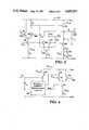
- FIG. 4Yet another embodiment of the present invention is shown in FIG. 4.
- the ECL line driver circuit 310 of FIG. 4contains all of the same components as the circuit of FIG. 2. However, the load resistor R1 is connected between the collector of the input transistor Q1 and the supply potential VCC. The base of the emitter follower transistor Q4 is connected to the collector of the input transistor Q1. The dynamic current enhancement circuit 18 within the dotted line is connected between the base and emitter of the transistor Q4 in a manner identical to that of FIG. 2. The output terminal 14 will now provide an output signal inverted from the input signal applied to input terminal 12. Except for these changes, the operation of the circuit 310 of FIG. 4 corresponds to the circuit 110 of FIG. 2. Alternately, additional load resistor, emitter follower transistor and dynamic current enhancement circuit could be connected to the input transistor Q1 of FIG. 2 if it is desired to speed up transitions on both the non-inverting and inverting output terminals.
- the present inventionprovides improved ECL line driver circuits for driving line loads having significant capacitance which includes a dynamic current enhancement circuit to speed up transitions at the output terminal.
- the ECL circuits of the present inventionutilizes a dynamic capacitance to provide a transient increase or decrease in the current through a current source enhancement transistor for speeding of the transition times.
Landscapes
- Engineering & Computer Science (AREA)
- Physics & Mathematics (AREA)
- Computer Hardware Design (AREA)
- Computing Systems (AREA)
- General Engineering & Computer Science (AREA)
- Mathematical Physics (AREA)
- Power Engineering (AREA)
- Logic Circuits (AREA)
Abstract
Description
Claims (8)
Priority Applications (1)
| Application Number | Priority Date | Filing Date | Title |
|---|---|---|---|
| US06/853,504US4687953A (en) | 1986-04-18 | 1986-04-18 | Dynamic ECL line driver circuit |
Applications Claiming Priority (1)
| Application Number | Priority Date | Filing Date | Title |
|---|---|---|---|
| US06/853,504US4687953A (en) | 1986-04-18 | 1986-04-18 | Dynamic ECL line driver circuit |
Publications (1)
| Publication Number | Publication Date |
|---|---|
| US4687953Atrue US4687953A (en) | 1987-08-18 |
Family
ID=25316213
Family Applications (1)
| Application Number | Title | Priority Date | Filing Date |
|---|---|---|---|
| US06/853,504Expired - LifetimeUS4687953A (en) | 1986-04-18 | 1986-04-18 | Dynamic ECL line driver circuit |
Country Status (1)
| Country | Link |
|---|---|
| US (1) | US4687953A (en) |
Cited By (17)
| Publication number | Priority date | Publication date | Assignee | Title |
|---|---|---|---|---|
| US4798973A (en)* | 1987-05-13 | 1989-01-17 | Texas Instruments Incorporated | High frequency charge pump/integrator circuit |
| US4835420A (en)* | 1987-11-17 | 1989-05-30 | Applied Micro Circuits Corporation | Method and apparatus for signal level conversion with clamped capacitive bootstrap |
| US4877977A (en)* | 1987-06-02 | 1989-10-31 | Fujitsu Limited | ECL circuit having an improved emitter follower output circuit |
| US4926065A (en)* | 1987-11-17 | 1990-05-15 | Applied Micro Circuits Corporation | Method and apparatus for coupling an ECL output signal using a clamped capacitive bootstrap circuit |
| US4928024A (en)* | 1988-05-13 | 1990-05-22 | Fujitsu Limited | Referenceless ECL logic circuit |
| US4948991A (en)* | 1988-11-03 | 1990-08-14 | Motorola Inc. | Load controlled ECL transient driver |
| US5027013A (en)* | 1987-11-17 | 1991-06-25 | Applied Micro Circuits Corporation | Method and apparatus for coupling an ECL output signal using a clamped capacitive bootstrap circuit |
| EP0440192A1 (en)* | 1990-01-31 | 1991-08-07 | Kabushiki Kaisha Toshiba | ECL circuit constituted in semiconductor integrated circuit |
| US5041747A (en)* | 1986-07-23 | 1991-08-20 | Tandem Computers Incorporated | Delay regulation circuit |
| US5045729A (en)* | 1989-11-15 | 1991-09-03 | National Semiconductor Corporation | TTL/ECL translator circuit |
| US5136179A (en)* | 1988-10-31 | 1992-08-04 | Teledyne Industries, Inc. | Logic level discriminator |
| US5146116A (en)* | 1989-11-30 | 1992-09-08 | Kabushiki Kaisha Toshida | Ecl circuit with a reduced power active pulldown |
| US5187391A (en)* | 1990-06-29 | 1993-02-16 | Nec Corporation | Modified non-threshold logic circuit |
| US5258667A (en)* | 1991-02-08 | 1993-11-02 | Nec Corporation | Logic circuit for controlling a supply on drive pulses to regulate an output level |
| US5321321A (en)* | 1991-08-30 | 1994-06-14 | Nec Corporation | Emitter-coupled logic (ECL) circuit with an inductively coupled output stage for enhanced operating speed |
| US5343092A (en)* | 1992-04-27 | 1994-08-30 | International Business Machines Corporation | Self-biased feedback-controlled active pull-down signal switching |
| US5764082A (en)* | 1996-07-29 | 1998-06-09 | Cirrus Logic, Inc. | Circuits, systems and methods for transferring data across a conductive line |
Citations (10)
| Publication number | Priority date | Publication date | Assignee | Title |
|---|---|---|---|---|
| US3978347A (en)* | 1974-10-02 | 1976-08-31 | Motorola, Inc. | High band width emitter coupled logic gate |
| US4092551A (en)* | 1976-05-20 | 1978-05-30 | International Business Machines Corporation | A.C. powered speed up circuit |
| JPS5368064A (en)* | 1976-11-29 | 1978-06-17 | Fujitsu Ltd | Non-saturation high-speed logical circuit |
| US4237388A (en)* | 1977-06-14 | 1980-12-02 | Nippon Electric Co., Ltd. | Inverter circuit |
| US4356409A (en)* | 1979-06-29 | 1982-10-26 | Hitachi, Ltd. | Level conversion circuit |
| US4449063A (en)* | 1979-08-29 | 1984-05-15 | Fujitsu Limited | Logic circuit with improved switching |
| JPS59115618A (en)* | 1982-12-22 | 1984-07-04 | Hitachi Ltd | Power supply circuit in bipolar lsi |
| US4533838A (en)* | 1981-12-18 | 1985-08-06 | Nippon Electric Co., Ltd. | Diode driver circuit having stored charge control means |
| US4539493A (en)* | 1983-11-09 | 1985-09-03 | Advanced Micro Devices, Inc. | Dynamic ECL circuit adapted to drive loads having significant capacitance |
| EP0177278A1 (en)* | 1984-09-28 | 1986-04-09 | Advanced Micro Devices, Inc. | Emitter coupled logic circuit |
- 1986
- 1986-04-18USUS06/853,504patent/US4687953A/ennot_activeExpired - Lifetime
Patent Citations (10)
| Publication number | Priority date | Publication date | Assignee | Title |
|---|---|---|---|---|
| US3978347A (en)* | 1974-10-02 | 1976-08-31 | Motorola, Inc. | High band width emitter coupled logic gate |
| US4092551A (en)* | 1976-05-20 | 1978-05-30 | International Business Machines Corporation | A.C. powered speed up circuit |
| JPS5368064A (en)* | 1976-11-29 | 1978-06-17 | Fujitsu Ltd | Non-saturation high-speed logical circuit |
| US4237388A (en)* | 1977-06-14 | 1980-12-02 | Nippon Electric Co., Ltd. | Inverter circuit |
| US4356409A (en)* | 1979-06-29 | 1982-10-26 | Hitachi, Ltd. | Level conversion circuit |
| US4449063A (en)* | 1979-08-29 | 1984-05-15 | Fujitsu Limited | Logic circuit with improved switching |
| US4533838A (en)* | 1981-12-18 | 1985-08-06 | Nippon Electric Co., Ltd. | Diode driver circuit having stored charge control means |
| JPS59115618A (en)* | 1982-12-22 | 1984-07-04 | Hitachi Ltd | Power supply circuit in bipolar lsi |
| US4539493A (en)* | 1983-11-09 | 1985-09-03 | Advanced Micro Devices, Inc. | Dynamic ECL circuit adapted to drive loads having significant capacitance |
| EP0177278A1 (en)* | 1984-09-28 | 1986-04-09 | Advanced Micro Devices, Inc. | Emitter coupled logic circuit |
Non-Patent Citations (8)
| Title |
|---|
| Barish et al, "Current Switch Push-Pull Internal Circuit"; IBM TDB; vol. 24, No. 6, p. 3041; 11/1981. |
| Barish et al, Current Switch Push Pull Internal Circuit ; IBM TDB; vol. 24, No. 6, p. 3041; 11/1981.* |
| Barry, "High Performance Current Switch Push-Pull Off-Chip Driver"; IBM TDB; vol. 26, No. 7B, pp. 3642-3643; 12/1983. |
| Barry, High Performance Current Switch Push Pull Off Chip Driver ; IBM TDB; vol. 26, No. 7B, pp. 3642 3643; 12/1983.* |
| Chan, "High Speed Current Switch Push-Pull Driver"; IBM TDB; vol. 24, No. 5, pp. 2635-2636; 10/1981. |
| Chan, High Speed Current Switch Push Pull Driver ; IBM TDB; vol. 24, No. 5, pp. 2635 2636; 10/1981.* |
| Chang et al, "Complementary Driver for Emitter-Coupled-Logic Gates"; IBM TDB; vol. 19, No. 12, pp. 4614-4615; 5/1977. |
| Chang et al, Complementary Driver for Emitter Coupled Logic Gates ; IBM TDB; vol. 19, No. 12, pp. 4614 4615; 5/1977.* |
Cited By (18)
| Publication number | Priority date | Publication date | Assignee | Title |
|---|---|---|---|---|
| US5041747A (en)* | 1986-07-23 | 1991-08-20 | Tandem Computers Incorporated | Delay regulation circuit |
| US4798973A (en)* | 1987-05-13 | 1989-01-17 | Texas Instruments Incorporated | High frequency charge pump/integrator circuit |
| US4877977A (en)* | 1987-06-02 | 1989-10-31 | Fujitsu Limited | ECL circuit having an improved emitter follower output circuit |
| US5027013A (en)* | 1987-11-17 | 1991-06-25 | Applied Micro Circuits Corporation | Method and apparatus for coupling an ECL output signal using a clamped capacitive bootstrap circuit |
| US4835420A (en)* | 1987-11-17 | 1989-05-30 | Applied Micro Circuits Corporation | Method and apparatus for signal level conversion with clamped capacitive bootstrap |
| US4926065A (en)* | 1987-11-17 | 1990-05-15 | Applied Micro Circuits Corporation | Method and apparatus for coupling an ECL output signal using a clamped capacitive bootstrap circuit |
| US4928024A (en)* | 1988-05-13 | 1990-05-22 | Fujitsu Limited | Referenceless ECL logic circuit |
| US5136179A (en)* | 1988-10-31 | 1992-08-04 | Teledyne Industries, Inc. | Logic level discriminator |
| US4948991A (en)* | 1988-11-03 | 1990-08-14 | Motorola Inc. | Load controlled ECL transient driver |
| US5045729A (en)* | 1989-11-15 | 1991-09-03 | National Semiconductor Corporation | TTL/ECL translator circuit |
| US5146116A (en)* | 1989-11-30 | 1992-09-08 | Kabushiki Kaisha Toshida | Ecl circuit with a reduced power active pulldown |
| EP0440192A1 (en)* | 1990-01-31 | 1991-08-07 | Kabushiki Kaisha Toshiba | ECL circuit constituted in semiconductor integrated circuit |
| US5122683A (en)* | 1990-01-31 | 1992-06-16 | Kabushiki Kaisha Toshiba | Ecl circuit with feedback controlled pull down in output |
| US5187391A (en)* | 1990-06-29 | 1993-02-16 | Nec Corporation | Modified non-threshold logic circuit |
| US5258667A (en)* | 1991-02-08 | 1993-11-02 | Nec Corporation | Logic circuit for controlling a supply on drive pulses to regulate an output level |
| US5321321A (en)* | 1991-08-30 | 1994-06-14 | Nec Corporation | Emitter-coupled logic (ECL) circuit with an inductively coupled output stage for enhanced operating speed |
| US5343092A (en)* | 1992-04-27 | 1994-08-30 | International Business Machines Corporation | Self-biased feedback-controlled active pull-down signal switching |
| US5764082A (en)* | 1996-07-29 | 1998-06-09 | Cirrus Logic, Inc. | Circuits, systems and methods for transferring data across a conductive line |
Similar Documents
| Publication | Publication Date | Title |
|---|---|---|
| US4687953A (en) | Dynamic ECL line driver circuit | |
| US4825101A (en) | Full-level, fast CMOS output buffer | |
| US4948991A (en) | Load controlled ECL transient driver | |
| US4902914A (en) | Logic circuit used in standard IC or CMOS logic level | |
| KR910009086B1 (en) | Output circuit | |
| US4985645A (en) | BiCMOS logic circuit having a rapid output voltage falling-down property | |
| US5309039A (en) | Power supply dependent input buffer | |
| EP0590247B1 (en) | BICMOS level converter circuit | |
| US5381057A (en) | ECL gate having active pull-down transistor | |
| US4002931A (en) | Integrated circuit bipolar bootstrap driver | |
| JPH05268031A (en) | Adjusted bicmos output buffer | |
| JPH0629824A (en) | Changeover circuit of logic signal | |
| US4675555A (en) | IC input buffer emitter follower with current source value dependent upon connection length for equalizing signal delay | |
| US4454432A (en) | Power efficient TTL buffer for driving large capacitive loads | |
| US4883975A (en) | Schmitt trigger circuit | |
| US5514984A (en) | Active pull down type ECL apparatus capable of stable operation | |
| JPS61293022A (en) | Ecl-ttl converting and outputting circuit | |
| JP2699823B2 (en) | Semiconductor integrated circuit | |
| JPH03147422A (en) | Ecl circuit | |
| US4967106A (en) | Emitter-coupled logic circuit | |
| EP0054408B1 (en) | Logic circuit | |
| JP2544826B2 (en) | Semiconductor integrated circuit | |
| US5187391A (en) | Modified non-threshold logic circuit | |
| US5382842A (en) | Composite logic circuit with bipolar transistor-complementary field effect transistor | |
| US5446400A (en) | GTL compatible BICMOS input stage |
Legal Events
| Date | Code | Title | Description |
|---|---|---|---|
| AS | Assignment | Owner name:ADVANCED MICRO DEVICES, INC., 901 THOMPSON PLACE, Free format text:ASSIGNMENT OF ASSIGNORS INTEREST.;ASSIGNOR:VARADARAJAN, HEMMIGE D.;REEL/FRAME:004565/0534 Effective date:19860417 | |
| STCF | Information on status: patent grant | Free format text:PATENTED CASE | |
| FPAY | Fee payment | Year of fee payment:4 | |
| FPAY | Fee payment | Year of fee payment:8 | |
| FPAY | Fee payment | Year of fee payment:12 | |
| AS | Assignment | Owner name:MORGAN STANLEY & CO. INCORPORATED, NEW YORK Free format text:SECURITY INTEREST;ASSIGNOR:LEGERITY, INC.;REEL/FRAME:011601/0539 Effective date:20000804 | |
| AS | Assignment | Owner name:LEGERITY, INC., TEXAS Free format text:ASSIGNMENT OF ASSIGNORS INTEREST;ASSIGNOR:ADVANCED MICRO DEVICES, INC.;REEL/FRAME:011700/0686 Effective date:20000731 | |
| AS | Assignment | Owner name:MORGAN STANLEY & CO. INCORPORATED, AS FACILITY COL Free format text:SECURITY AGREEMENT;ASSIGNORS:LEGERITY, INC.;LEGERITY HOLDINGS, INC.;LEGERITY INTERNATIONAL, INC.;REEL/FRAME:013372/0063 Effective date:20020930 | |
| AS | Assignment | Owner name:SAXON IP ASSETS LLC, TEXAS Free format text:ASSIGNMENT OF ASSIGNORS INTEREST;ASSIGNOR:LEGERITY, INC.;REEL/FRAME:017537/0307 Effective date:20060324 | |
| AS | Assignment | Owner name:LEGERITY INTERNATIONAL, INC., TEXAS Free format text:RELEASE OF SECURITY INTEREST;ASSIGNOR:MORGAN STANLEY SENIOR FUNDING INC., AS ADMINISTRATIVE AGENT, SUCCESSOR TO MORGAN STANLEY & CO. INCORPORATED, AS FACILITY COLLATERAL AGENT;REEL/FRAME:019699/0854 Effective date:20070727 Owner name:LEGERITY HOLDINGS, INC., TEXAS Free format text:RELEASE OF SECURITY INTEREST;ASSIGNOR:MORGAN STANLEY SENIOR FUNDING INC., AS ADMINISTRATIVE AGENT, SUCCESSOR TO MORGAN STANLEY & CO. INCORPORATED, AS FACILITY COLLATERAL AGENT;REEL/FRAME:019699/0854 Effective date:20070727 Owner name:LEGERITY, INC., TEXAS Free format text:RELEASE OF SECURITY INTEREST;ASSIGNOR:MORGAN STANLEY SENIOR FUNDING INC., AS ADMINISTRATIVE AGENT, SUCCESSOR TO MORGAN STANLEY & CO. INCORPORATED, AS FACILITY COLLATERAL AGENT;REEL/FRAME:019699/0854 Effective date:20070727 Owner name:LEGERITY, INC., TEXAS Free format text:RELEASE OF SECURITY INTEREST;ASSIGNOR:MORGAN STANLEY SENIOR FUNDING INC., AS ADMINISTRATIVE AGENT, SUCCESSOR TO MORGAN STANLEY & CO. INCORPORATED;REEL/FRAME:019690/0647 Effective date:20070727 | |
| AS | Assignment | Owner name:SAXON INNOVATIONS, LLC, TEXAS Free format text:ASSIGNMENT OF ASSIGNORS INTEREST;ASSIGNOR:SAXON IP ASSETS, LLC;REEL/FRAME:020261/0892 Effective date:20071016 | |
| AS | Assignment | Owner name:RPX CORPORATION,CALIFORNIA Free format text:ASSIGNMENT OF ASSIGNORS INTEREST;ASSIGNOR:SAXON INNOVATIONS, LLC;REEL/FRAME:024202/0302 Effective date:20100324 |