US4683637A - Forming depthwise isolation by selective oxygen/nitrogen deep implant and reaction annealing - Google Patents
Forming depthwise isolation by selective oxygen/nitrogen deep implant and reaction annealingDownload PDFInfo
- Publication number
- US4683637A US4683637AUS06/826,951US82695186AUS4683637AUS 4683637 AUS4683637 AUS 4683637AUS 82695186 AUS82695186 AUS 82695186AUS 4683637 AUS4683637 AUS 4683637A
- Authority
- US
- United States
- Prior art keywords
- substrate
- dielectric
- region
- depth
- nitrogen
- Prior art date
- Legal status (The legal status is an assumption and is not a legal conclusion. Google has not performed a legal analysis and makes no representation as to the accuracy of the status listed.)
- Expired - Lifetime
Links
Images


Classifications
- H—ELECTRICITY
- H10—SEMICONDUCTOR DEVICES; ELECTRIC SOLID-STATE DEVICES NOT OTHERWISE PROVIDED FOR
- H10D—INORGANIC ELECTRIC SEMICONDUCTOR DEVICES
- H10D30/00—Field-effect transistors [FET]
- H10D30/60—Insulated-gate field-effect transistors [IGFET]
- H—ELECTRICITY
- H01—ELECTRIC ELEMENTS
- H01L—SEMICONDUCTOR DEVICES NOT COVERED BY CLASS H10
- H01L21/00—Processes or apparatus adapted for the manufacture or treatment of semiconductor or solid state devices or of parts thereof
- H01L21/02—Manufacture or treatment of semiconductor devices or of parts thereof
- H01L21/04—Manufacture or treatment of semiconductor devices or of parts thereof the devices having potential barriers, e.g. a PN junction, depletion layer or carrier concentration layer
- H01L21/18—Manufacture or treatment of semiconductor devices or of parts thereof the devices having potential barriers, e.g. a PN junction, depletion layer or carrier concentration layer the devices having semiconductor bodies comprising elements of Group IV of the Periodic Table or AIIIBV compounds with or without impurities, e.g. doping materials
- H01L21/26—Bombardment with radiation
- H01L21/263—Bombardment with radiation with high-energy radiation
- H01L21/265—Bombardment with radiation with high-energy radiation producing ion implantation
- H01L21/26506—Bombardment with radiation with high-energy radiation producing ion implantation in group IV semiconductors
- H01L21/26533—Bombardment with radiation with high-energy radiation producing ion implantation in group IV semiconductors of electrically inactive species in silicon to make buried insulating layers
- H—ELECTRICITY
- H01—ELECTRIC ELEMENTS
- H01L—SEMICONDUCTOR DEVICES NOT COVERED BY CLASS H10
- H01L21/00—Processes or apparatus adapted for the manufacture or treatment of semiconductor or solid state devices or of parts thereof
- H01L21/70—Manufacture or treatment of devices consisting of a plurality of solid state components formed in or on a common substrate or of parts thereof; Manufacture of integrated circuit devices or of parts thereof
- H01L21/71—Manufacture of specific parts of devices defined in group H01L21/70
- H01L21/76—Making of isolation regions between components
- H01L21/762—Dielectric regions, e.g. EPIC dielectric isolation, LOCOS; Trench refilling techniques, SOI technology, use of channel stoppers
- H01L21/7624—Dielectric regions, e.g. EPIC dielectric isolation, LOCOS; Trench refilling techniques, SOI technology, use of channel stoppers using semiconductor on insulator [SOI] technology
- H01L21/76264—SOI together with lateral isolation, e.g. using local oxidation of silicon, or dielectric or polycristalline material refilled trench or air gap isolation regions, e.g. completely isolated semiconductor islands
- H01L21/76267—Vertical isolation by silicon implanted buried insulating layers, e.g. oxide layers, i.e. SIMOX techniques
- H—ELECTRICITY
- H01—ELECTRIC ELEMENTS
- H01L—SEMICONDUCTOR DEVICES NOT COVERED BY CLASS H10
- H01L21/00—Processes or apparatus adapted for the manufacture or treatment of semiconductor or solid state devices or of parts thereof
- H01L21/70—Manufacture or treatment of devices consisting of a plurality of solid state components formed in or on a common substrate or of parts thereof; Manufacture of integrated circuit devices or of parts thereof
- H01L21/71—Manufacture of specific parts of devices defined in group H01L21/70
- H01L21/76—Making of isolation regions between components
- H01L21/762—Dielectric regions, e.g. EPIC dielectric isolation, LOCOS; Trench refilling techniques, SOI technology, use of channel stoppers
- H01L21/7624—Dielectric regions, e.g. EPIC dielectric isolation, LOCOS; Trench refilling techniques, SOI technology, use of channel stoppers using semiconductor on insulator [SOI] technology
- H01L21/76264—SOI together with lateral isolation, e.g. using local oxidation of silicon, or dielectric or polycristalline material refilled trench or air gap isolation regions, e.g. completely isolated semiconductor islands
- H01L21/76283—Lateral isolation by refilling of trenches with dielectric material
- Y—GENERAL TAGGING OF NEW TECHNOLOGICAL DEVELOPMENTS; GENERAL TAGGING OF CROSS-SECTIONAL TECHNOLOGIES SPANNING OVER SEVERAL SECTIONS OF THE IPC; TECHNICAL SUBJECTS COVERED BY FORMER USPC CROSS-REFERENCE ART COLLECTIONS [XRACs] AND DIGESTS
- Y10—TECHNICAL SUBJECTS COVERED BY FORMER USPC
- Y10S—TECHNICAL SUBJECTS COVERED BY FORMER USPC CROSS-REFERENCE ART COLLECTIONS [XRACs] AND DIGESTS
- Y10S148/00—Metal treatment
- Y10S148/077—Implantation of silicon on sapphire
- Y—GENERAL TAGGING OF NEW TECHNOLOGICAL DEVELOPMENTS; GENERAL TAGGING OF CROSS-SECTIONAL TECHNOLOGIES SPANNING OVER SEVERAL SECTIONS OF THE IPC; TECHNICAL SUBJECTS COVERED BY FORMER USPC CROSS-REFERENCE ART COLLECTIONS [XRACs] AND DIGESTS
- Y10—TECHNICAL SUBJECTS COVERED BY FORMER USPC
- Y10S—TECHNICAL SUBJECTS COVERED BY FORMER USPC CROSS-REFERENCE ART COLLECTIONS [XRACs] AND DIGESTS
- Y10S148/00—Metal treatment
- Y10S148/082—Ion implantation FETs/COMs
Definitions
- This inventionrelates in general to means and methods for semiconductor devices and, more particularly to means and methods for partially dielectrically isolated, self-aligned, semiconductor devices.
- dielectrically isolated (DIC) deviceswere formed by first etching a mesh shaped pattern of grooves in the upper surface of a single crystal semiconductor substrate so as to leave islands of single crystal material between the grooves, coating the grooves and the exposed islands with a dielectric layer, covering the dielectric layer with a thick polycrystalline layer, and then grinding away the single crystal substrate so as to expose the islands of single crystal material.
- Thisprovided a structure in which each single crystal island was surrounded by a dielectric region embedded in a polycrystalline matrix. Individual devices could then be fabricated in the individual single crystal semiconductor islands. While this arrangement was satisfactory for building low density integrated circuits, particularly radiation hardened integrated circuits, it has not proved well suited to high density and large scale integrated circuits.
- dielectrically isolated circuitshave been prepared by taking a single crystal substrate, blanket implanting a very high dose of oxygen at an energy sufficient to place the peak of the implanted oxygen distribution well below the substrate surface.
- the implanted oxygenforms a thin buried dielectric layer.
- the implanted substrateis heated so as to anneal, in so far as possible, the structural damage in the single crystal semiconductor region between the surface and the implanted dielectric layer.
- a single crystal semiconductor substratehaving a first surface; a first insulating dielectric region (e.g., a gate insulator) on a portion of the first surface; a conductor means (e.g., a gate electrode) above the first dielectric region; first and second single crystal semiconductor regions (e.g., source and drain regions) in the substrate extending below the first surface a first pre-determined distance and lying on either side of the first dielectric region; second insulating dielectric regions (e.g., buried dielectric isolation regions) in the substrate underlying the first and second single crystal semiconductor regions and not substantially extending under the first dielectric region; and third dielectric regions (e.g., lateral isolation walls) in the substrate extending from the surface to the second dielectric regions and laterally separated from the first dielectric region by the first and second single crystal semiconductor regions.
- first insulating dielectric regione.g., a gate insulator
- a conductor meanse.g., a gate electrode
- first and second single crystal semiconductor regions
- a method for fabricating a semiconductor devicecomprising: providing a single crystal semiconductor substrate having a first surface; forming on or above the first surface a gate conductor means having a first pre-determined thickness and overlying a first region of the substrate and not overlying a first region of substrate; and implanting oxygen or nitrogen into a first part of the second region of the substrate to a dose exceeding about 1 ⁇ 10 18 ions/cm 2 , preferably exceeding about 1.7 ⁇ 10 18 ions/cm 2 , to form a buried dielectric layer in the second region, wherein the implant energy is sufficient to cause the ions to penetrate into the substrate to a second pre-determined depth and not penetrate through the gate conductor means into the first region of the substrate. It is desirable to include the step of forming lateral dielectric isolation walls extending from the first surface to the buried dielectric layer. These lateral dielectric isolation walls may be formed before or after forming the buried dielectric layer.
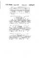
- FIGS. 1-4, 4A, and 5-11show simplified schematic cross-sectional views of a portion of a semiconductor device, according to the present invention, at different stages of fabrication, and according to different embodiments.
- the device structures and methods hereinare illustrated for the case of silicon based semiconductor devices using silicon oxide and silicon nitride dielectric layers and polysilicon layers.
- silicon oxide and silicon nitride dielectric layers and polysilicon layersare examples of semiconductor materials.
- the described means and methodsapply to other semiconductor substrates, other dielectric materials, and other polcrystalline semiconductor layers, and that the illustrated examples are merely presented as an aid to understanding and not intended to be limiting, and that other materials may also be used.
- dielectric layers or regionsare shown hatched, polycrystalline semiconductor regions are shown stippled, and single crystal regions, metal layers, and masking layers are shown clear.
- Arrowsare used to indicate conventional implanation and/or bombardment etching techniques, such as for example, reactive ion etching or ion milling. It will be understood by those of skill in the art that masking, etching, and doping may be carried out by other means well known in the art.
- FIGS. 1-4, 4A, and 5-11show in simplified schematic cross-sectional form, a portion of a semiconductor device according to the present invention during different stages of fabrication and for different embodiments.
- the means and method of the present inventionare best understood by considering the figures sequentially.
- device portion 9consists of substrate 10 of, for example, single crystal silicon, on which has been provided dielectric layers 11 and 12.
- Dielectric layer 11is, for silicon substrates, conveniently formed of silicon dioxide. Thicknesses of layer 11 in the range 0.01-0.08 microns are useful. However, larger or smaller thicknesses may also be used.
- Layer 12is conveniently formed of silicon nitride of a thickness in the range 0.05-0.3 microns. It is important that layer 12 be resistant to oxygen migration, since in a subsequent step it will be used to locally control the oxidation of substrate 10. Layer 12 may be of any material which provides this oxidation masking function and does not otherwise contaminate substrate 10.
- Layer 12is covered with masking layer 13 (FIG. 2) of any convenient material. Photoresist is a typical example. Layer 13 is patterned to provide openings as indicated in FIG. 2 through which holes 15 are etched successively in layers 12, and 11, so as to locally expose portions of the surface of substrate 10. Means for etching layers 12 and 11 are well known in the art. Trenches 15 are then etched in substrate 10, for example by reactive ion etching as indicated by arrows 14. Trenches 15 are then filled with dielectric regions 16 as indicated in FIG. 3. Each dielectric region 16 serves as a lateral isolation wall. This is conveniently accomplished by oxidation of substrate 10, but other means well known in the art may also be used.
- isolation walls 16are formed by oxidation
- layer 12serves as an oxidation mask to prevent generalized oxidation of substrate 10 (see FIG. 3). It is desirable that trenches 15 be filled so that the surfaces of dielectric isolation walls 16 are substantially level with the surface of dielectric layer 11, however this is not essential.
- Isolation walls 16 and dielectric layer 11are then covered with conductor layer 17 of thickness 60, as shown in FIG. 4.
- Layer 17is conveniently of, for example, polycrystalline silicon, but other conductor materials may also be used.
- region 11a of device portion 9may conveniently serve as the gate dielectric of a MOSFET. Thickness 8 of dielectric layer 11 may be chosen so that it provides the desired thickness for the gate insulator, however this is not essential.
- the central portion of layer 11 between edges 11bmay be striped from substrate 10 prior to depositing layer 17 and new dielectric layer 11c of any desired thickness 7 formed in central region 11b--11b between isolation walls 16.
- Dielectric layer portion 11cmay be formed by oxidation of substrate 10 or by any other convenient technique and may be of any desired material. Means for stripping the central portion of dielectric layer 11 and providing new dielectric layer 11c are well known in the art and are conventional.
- layer 11 in FIGS. 1-4may be omitted and layer 12 placed directly on substrate 10. If an oxide or other dielectric layer analogous to layer 11 is needed on substrate 10 for other purposes, it may be formed at the same time as layer 11c.
- dielectric region 11cis not essential and may be omitted.
- JFETS, MESFETS, and bipolar transistorsare examples of devices which do not require an insulator such as dielectric region 11c.
- FIGS. 5-11it is assumed that the configuration illustrated in FIG. 4 has been utilized. Those of skill in the art will understand that other configurations could equally well have been employed.
- a masking layer(not shown) is formed on layer 17 so as to cover or protect portions 17a while leaving portions 17aa exposed (FIG. 4). Portions 17aa are then removed while portion 17a is left substantially undisturbed (FIG. 5).
- Masking and etching techniques for removing portions 17aa while leaving portion 17a undisturbedare well known in the art and are conventional. It is desirable to employ masking and etching procedures which provide substantially vertical sidewalls on portion 17a. Reactive ion etching and ion milling are examples of known techniques for producing substantially vertical sidewalls but others may also be used.
- ions 18 of, for example, oxygen or nitrogen or mixtures thereofare implanted with ions 18 of, for example, oxygen or nitrogen or mixtures thereof, to a dose sufficient to form buried dielectric layer or region 19.
- the implant energymust be sufficient to locate buried dielectric layer 19 at depth 40 below surface 10f of substrate 10.
- Doses of oxygen or nitrogen or a combination thereof exceeding about 1 ⁇ 10 18 ions/cm 2are necessary to form buried dielectric region 19.
- Doses in the range 1.7-2.2 ⁇ 10 18 ions/cm 2are convenient.
- Energys exceeding about 80 KeVare useful, with 150 KeV being typical. Higher energies can also be used. It is convenient to carry out the oxygen/nitrogen implant through dielectric layer 11.
- the dose and energyare selected, using means well known in the art, so that portions 10b-c of substrate 10 having thickness 40 lie between buried dielectric layer 19 and surface 10f of substrate 10.
- range 41 to the center of implanted region of layer 19is about 0.37 microns at 150 KeV. This range includes thickness 50 of about 0.025 microns for covering oxide 11.
- Increasing the dose beyond the levels indicated aboveincreases thickness 51 of buried dielectric layer 19.
- Increasing the implant energyincreases distance 41 from exposed surface 30 to the center of implanted dielectric layer 19.
- the quality of implanted buried dielectric layer 19 and the quality of overlying single crystal regions 10b-care improved by annealing the structure after oxygen or nitrogen implanation. Annealing removes some of the implant damage created in single crystal regions 10b-c above buried dielectric layer 19 as a result of the oxygen or nitrogen implant, and also densifies buried dielectric layer 19. In general, some implant damage or dislocations always remain in regions 10b-c.
- Annealing temperatures exceeding about 1000° C.are desirable, with temperatures exceeding 1100° C. being preferred and about 1150° C. being convenient.
- Annealing timevaries inversely with temperature, the higher the temperature the shorter the time required to obtain a given annealing effect.
- annealing times in the range 1-4 hoursare satisfactory.
- longer or shorter timescan also be used with lower or higher temperatures. For example, 2-3 minutes at about 1400° C. has about the same effect as 1-2 hours at 1100°-1500° C.
- Annealing of the oxygen/nitrogen implantis conveniently carried out in an inert ambient, e.g. argon. A small amount of oxygen may be added briefly to promote regrowth of any part of layer 11 which has been eroded by sputtering during the oxygen/nitrogen implant.
- Annealing the oxygen/nitrogen implant damage prior to dopingavoids having the oxygen/nitrogen annealing step cause redistribution of the dopants. However, this is not essential.
- a blanket implant for ions 18It is desirable to use a blanket implant for ions 18.
- buried dielectric zone 17cis formed in region 17a at the same time as buried dielectric layer 19 is formed in substrate 10 (see FIG. 5). Since it is an objective of the present invention to avoid implant damage in region 10e undeneath dielectric portion 11a and conductor portion 17a, thickness 61 of conductor region 17a must be larger than implant depth 42 in the material of conductor 17.
- dielectric zone 17c formed by implanted ions 18 in conductor portion 17alies at distance 43 away from sensitive dielectric region 11a. While upper portion 17b of region 17a may experience substantial implant damage, lower portion 17d protects underlying regions 11a and 10e so that they are substantially free of direct implant damage.
- regions 10b-cwill experience significant implant damage during formation of buried dielectric layer 19.
- region 10e of substrate 10will be substantially free of implant damage from ions 18. This is because region 10e is protected by conductor portion 17a during the oxygen/nitrogen implant. Boundaries 10d of dielectric regions 19c and implant damaged regions 10c may extend slightly under the edges of portion 17a, as illustrated in FIGS. 5-11. This is due in part to scattering effects. However, this slight intrusion is not sufficient to cause the ends of regions 19c to meet under portion 17a for device dimensions of practical interest, so region 10e remains substantially free of oxygen/nitrogen implant damage and remains directly coupled to underlying substrate 10a.
- Portion 17b of region 17ais then conveniently removed.
- Portion 17bmay be removed by direct etching, i.e., by etching with an etching means that directly attacks portion 17b, or portion 17b may be removed by lift-off using an etching means which attacks region 17c. Dip etching is convenient.
- region 17cPrior to annealing oxygen/nitrogen implanted region 17c, region 17c is porous and etches more rapidly than dielectric layer 11, even if formed of the same material, e.g. silicon oxide. Thus lift-off etching may be performed without a masking step, although a mask may be used if desired.
- mask 20 having opening 21--21is then applied to layer 11 on substrate 10 by conventional means well known in the art.
- conventional etching technqiuessuch as for example reactive ion etching as indicated by arrows 22
- portions 11d of oxide layer 11 between edges 11e--11eare removed. If dielectric region 17c has been left in place it is also conveniently removed at the same time. This exposes portion 17d of conductor region 17a and surface 10f of portions 10c of substrate 10 on either side of portion 17d.
- Portions 10c and 17dare then conveniently doped, as for example by ion implanation as indicated by arrows 23 (FIG. 7).
- the substrateis then heated to anneal any residual dopant implant damage and activate the dopant. This results typically in a lateral migration of the dopant placed in regions 10c so that the PN junctions formed by the dopant ions with the material of substrate 10 are at locations 10g under remaining portion 17d of conductor region 17a. (See FIG. 7).
- Portion 11d of dielectric layer 11may be left in place during implant doping of regions 10c by ions 23.
- the device illustrated in FIG. 7has conveniently the form of a MOS transistor. Regions 10c form the source and drain and portion 17d forms the gate with portion 11a acting as the gate dielectric. It will be observed from FIG. 7 that source-drain regions 10c are isolated from substrate 10 by dielectric regions 19c and from portions 10b by lateral dielectric isolation walls 16. Portions 10b of substrate 10 are similarly isolated from common region 10a of substrate 10 by dielectric portions 19b of buried dielectric layer 19.
- the channel of the MOS deviceis located between junctions 10g in region 10e.
- Portion 10a of substrate 10therefore forms a body or backgate contact to the channel.
- providing dielectric isolation regions 19c under source-drain regions 10c and dielectric isolation walls 16 laterally disposed on either side of regions 10csubstantially reduces the parasitic leakage currents and parasitic capacitances associated with the MOS device. This permits significantly improved device and circuit performance.
- source-drain regions 10care automatically self-aligned with gate region 17d without need for any separate masking or alignment steps.
- portion 17d and regions 10cmay utilize the minimum resolvable dimensions since it is not necessary to make an alignment therebetween. This permits much higher packing densities and substantially improved circuit performance.
- FIGS. 8-11illustrate an alternate embodiment of the means and method of the present invention. Unless otherwise indicated, FIGS. 8-10 are analogous to FIGS. 5-7, and regions or parts having the same numbers are identical.
- FIG. 8differs from FIG. 5 in that thick mask layer 24 having opening 24a is placed over layer 11 on substrate 10 prior to implanting ions 18.
- Mask 24must have sufficient thickness so as to prevent ions 18 from reaching substrate 10.
- Mask 24 with opening 24a--24aneed not be precision aligned to the pre-existing images on the wafer since it may be placed anywhere within the lateral extent of dielectric isolation walls 16.
- the purpose of mask 24is to prevent ions 18 from forming buried dielectric regions 19b (see FIG. 5) laterally exterior to dielectric isolation walls 16.
- Mask 24may be conveniently formed from high temperature materials such as oxides, nitrides, polysilicon or other refractory materials. High temperature materials are desirable because they are better able to withstand the elevated temperatures generated during the oxygen/nitrogen implant, e.g., 300°-800° C.
- FIG. 9is analogous to FIG. 6 except that sidewall dielectric regions 17e are formed on either side of portion 17d of conductor region 17a. This is conveniently accomplished by oxidation or other means well known in the art.
- mask layer 20is applied and the process proceeds in the same manner as previously described in connection with FIGS. 6 and 7.
- FIG. 10is analogous to FIG. 7 and illustrates the configuration when dielectric sidewalls 17e are present at the sides of portion 17d.
- FIG. 10also illustrates a further optional embodiment in that mask 20 is left in place during doping of regions 10c and 17d by ions 23. The purpose of mask 20 at this step is to prevent ions 23 from doping portions 10b of substrate 10 laterally outside dielectric isolation wall 16.
- the device of FIG. 10conveniently forms an MOS transistor.
- FIG. 11illustrates the configuration when contact conductors 26 having source contact 26a, drain contact 26b and gate contact 26c are applied to the structure of FIG. 10.
- the structure of FIG. 11conveniently forms a MOS transistor in which portions 10c are the source and drain and portion 17d is the gate.
- the channel region of this MOS transistoris formed under dielectric region 11a in portion 10e of substrate 10.
- Portion 10a of substrate 10 below dielectric layer 19provides a common body or backgate contact to the MOS transistors formed in this manner.
- portion 17ashields region 10e where the active device behavior takes place from damage due to ions 18 and ions 23 which are used to form buried dielectric layer 19 and to dope regions 10c. This is a significant advantage and substantially improves device behavior.
- the invented means and methodhave been illustrated in terms of MOS devices built on silicon substrates using buried dielectric layers formed with oxygen and/or nitrogen, those of skill in the art will understand that other materials may be used and other types of devices formed in both silicon and in other semiconductor materials.
- the means and method of the present inventionare particularly useful when it is desired that the active region of the device, e.g., the channel region of a MOSFET, the base or collector blocking region of a bipolar transistor or thyristor, or the depletion region of a diode, be protected during the high dose, high energy implants necessary to form the buried dielectric layer which is to isolate the non-active regions of the device from the common substrate.
- a significant advantage of the invented means and method as compared to prior art blanket implant structures and methodsis the suitability of the invented means and methods for use in CCDs and DRAMs and other devices in which the active device behavior is particularly sensitive to material defects.
- the invented means and methodreduces structural defects, reduces or eliminates oxygen donor compensation, improves mobility and minority carrier lifetimes, reduces channel-off currents, reduces parasitic latch-up problems, reduces soft-error charge upsets, and improves thin oxide integrity.
- a significant advantage over more conventional blanket isolated structuresis that a high tolerance to ionizing radiation can be achieved without increasing the number of defects in the sensitive regions of the device.
Landscapes
- Physics & Mathematics (AREA)
- Engineering & Computer Science (AREA)
- High Energy & Nuclear Physics (AREA)
- Condensed Matter Physics & Semiconductors (AREA)
- General Physics & Mathematics (AREA)
- Manufacturing & Machinery (AREA)
- Computer Hardware Design (AREA)
- Microelectronics & Electronic Packaging (AREA)
- Power Engineering (AREA)
- Health & Medical Sciences (AREA)
- Toxicology (AREA)
- Element Separation (AREA)
Abstract
Description
Claims (7)
Priority Applications (5)
| Application Number | Priority Date | Filing Date | Title |
|---|---|---|---|
| US06/826,951US4683637A (en) | 1986-02-07 | 1986-02-07 | Forming depthwise isolation by selective oxygen/nitrogen deep implant and reaction annealing |
| KR1019870700901AKR940011479B1 (en) | 1986-02-07 | 1986-11-26 | Semiconductor device manufacturing method |
| PCT/US1986/002540WO1987004860A1 (en) | 1986-02-07 | 1986-11-26 | Partially dielectrically isolated semiconductor devices |
| JP62500062AJPH0754825B2 (en) | 1986-02-07 | 1986-11-26 | Partial dielectric isolation semiconductor device |
| EP19870900416EP0258271A4 (en) | 1986-02-07 | 1986-11-26 | Partially dielectrically isolated semiconductor devices |
Applications Claiming Priority (1)
| Application Number | Priority Date | Filing Date | Title |
|---|---|---|---|
| US06/826,951US4683637A (en) | 1986-02-07 | 1986-02-07 | Forming depthwise isolation by selective oxygen/nitrogen deep implant and reaction annealing |
Publications (1)
| Publication Number | Publication Date |
|---|---|
| US4683637Atrue US4683637A (en) | 1987-08-04 |
Family
ID=25247929
Family Applications (1)
| Application Number | Title | Priority Date | Filing Date |
|---|---|---|---|
| US06/826,951Expired - LifetimeUS4683637A (en) | 1986-02-07 | 1986-02-07 | Forming depthwise isolation by selective oxygen/nitrogen deep implant and reaction annealing |
Country Status (5)
| Country | Link |
|---|---|
| US (1) | US4683637A (en) |
| EP (1) | EP0258271A4 (en) |
| JP (1) | JPH0754825B2 (en) |
| KR (1) | KR940011479B1 (en) |
| WO (1) | WO1987004860A1 (en) |
Cited By (60)
| Publication number | Priority date | Publication date | Assignee | Title |
|---|---|---|---|---|
| US4810664A (en)* | 1986-08-14 | 1989-03-07 | Hewlett-Packard Company | Method for making patterned implanted buried oxide transistors and structures |
| US4914046A (en)* | 1989-02-03 | 1990-04-03 | Motorola, Inc. | Polycrystalline silicon device electrode and method |
| US4959329A (en)* | 1988-03-28 | 1990-09-25 | Mitsubishi Denki Kabushiki Kaisha | Semiconductor device |
| US4963502A (en)* | 1988-08-25 | 1990-10-16 | Texas Instruments, Incorporated | Method of making oxide-isolated source/drain transistor |
| US5116774A (en)* | 1991-03-22 | 1992-05-26 | Motorola, Inc. | Heterojunction method and structure |
| US5185279A (en)* | 1987-03-31 | 1993-02-09 | Kabushiki Kaisha Toshiba | Method of manufacturing insulated-gate type field effect transistor |
| US5340766A (en)* | 1992-03-19 | 1994-08-23 | Nec Corporation | Method for fabricating charge-coupled device |
| US5399507A (en)* | 1994-06-27 | 1995-03-21 | Motorola, Inc. | Fabrication of mixed thin-film and bulk semiconductor substrate for integrated circuit applications |
| US5449630A (en)* | 1994-05-03 | 1995-09-12 | United Microelectronics Corp. | Method for fabricating a trench capacitor structure for dynamic random access memory integrated circuit |
| US5567629A (en)* | 1993-09-01 | 1996-10-22 | Kabushiki Kaisha Toshiba | Method of making transistor with oxygen implanted region |
| US5616509A (en)* | 1994-09-28 | 1997-04-01 | Nec Corporation | Method for fabricating a semiconductor device |
| US5702957A (en)* | 1996-09-20 | 1997-12-30 | Lsi Logic Corporation | Method of making buried metallization structure |
| US5705440A (en)* | 1995-09-13 | 1998-01-06 | Samsung Electronics Co., Ltd. | Methods of fabricating integrated circuit field effect transistors having reduced-area device isolation regions |
| US5712173A (en)* | 1996-01-24 | 1998-01-27 | Advanced Micro Devices, Inc. | Method of making semiconductor device with self-aligned insulator |
| US5849621A (en)* | 1996-06-19 | 1998-12-15 | Advanced Micro Devices, Inc. | Method and structure for isolating semiconductor devices after transistor formation |
| US5882974A (en)* | 1998-04-08 | 1999-03-16 | Advanced Micro Devices, Inc. | High-performance PMOS transistor using a barrier implant in the source-side of the transistor channel |
| US5908313A (en)* | 1996-12-31 | 1999-06-01 | Intel Corporation | Method of forming a transistor |
| US5930642A (en)* | 1997-06-09 | 1999-07-27 | Advanced Micro Devices, Inc. | Transistor with buried insulative layer beneath the channel region |
| US5972751A (en)* | 1998-08-28 | 1999-10-26 | Advanced Micro Devices, Inc. | Methods and arrangements for introducing nitrogen into a tunnel oxide in a non-volatile semiconductor memory device |
| US6057214A (en)* | 1996-12-09 | 2000-05-02 | Texas Instruments Incorporated | Silicon-on-insulation trench isolation structure and method for forming |
| US6066530A (en)* | 1998-04-09 | 2000-05-23 | Advanced Micro Devices, Inc. | Oxygen implant self-aligned, floating gate and isolation structure |
| US6069054A (en)* | 1997-12-23 | 2000-05-30 | Integrated Device Technology, Inc. | Method for forming isolation regions subsequent to gate formation and structure thereof |
| US6100148A (en)* | 1997-12-19 | 2000-08-08 | Advanced Micro Devices, Inc. | Semiconductor device having a liner defining the depth of an active region, and fabrication thereof |
| US6107150A (en)* | 1998-09-04 | 2000-08-22 | Advanced Micro Devices, Inc. | Method of making high performance transistors using channel modulated implant for ultra thin oxide formation |
| US6194259B1 (en)* | 1997-06-27 | 2001-02-27 | Advanced Micro Devices, Inc. | Forming retrograde channel profile and shallow LLDD/S-D extensions using nitrogen implants |
| US6198142B1 (en) | 1998-07-31 | 2001-03-06 | Intel Corporation | Transistor with minimal junction capacitance and method of fabrication |
| US6200836B1 (en) | 1999-08-06 | 2001-03-13 | Taiwan Semiconductor Manufacturing Company | Using oxide junction to cut off sub-threshold leakage in CMOS devices |
| WO2001029897A1 (en)* | 1999-10-20 | 2001-04-26 | Advanced Micro Devices, Inc. | Field effect transistor with non-floating body and method for forming same on a bulk silicon wafer |
| US6245636B1 (en) | 1999-10-20 | 2001-06-12 | Advanced Micro Devices, Inc. | Method of formation of pseudo-SOI structures with direct contact of transistor body to the substrate |
| US6258693B1 (en) | 1997-12-23 | 2001-07-10 | Integrated Device Technology, Inc. | Ion implantation for scalability of isolation in an integrated circuit |
| US6287897B1 (en)* | 2000-02-29 | 2001-09-11 | International Business Machines Corporation | Gate dielectric with self forming diffusion barrier |
| US6326665B1 (en)* | 1998-02-04 | 2001-12-04 | Hyundai Electronics Industries Co., Ltd. | Semiconductor device with insulating films |
| US20020037627A1 (en)* | 2000-08-10 | 2002-03-28 | Liu Mark Y. | Extension of shallow trench isolation by ion implantation |
| US6461902B1 (en)* | 2000-07-18 | 2002-10-08 | Institute Of Microelectronics | RF LDMOS on partial SOI substrate |
| US6465852B1 (en) | 1999-10-20 | 2002-10-15 | Advanced Micro Devices, Inc. | Silicon wafer including both bulk and SOI regions and method for forming same on a bulk silicon wafer |
| US6469350B1 (en) | 2001-10-26 | 2002-10-22 | International Business Machines Corporation | Active well schemes for SOI technology |
| US6475868B1 (en)* | 1999-08-18 | 2002-11-05 | Advanced Micro Devices, Inc. | Oxygen implantation for reduction of junction capacitance in MOS transistors |
| US6514809B1 (en) | 2000-11-03 | 2003-02-04 | Advanced Micro Devices, Inc. | SOI field effect transistors with body contacts formed by selective etch and fill |
| US6548345B2 (en)* | 1999-06-16 | 2003-04-15 | International Business Machines Corporation | Method of fabricating trench for SOI merged logic DRAM |
| US20030092222A1 (en)* | 2001-11-09 | 2003-05-15 | Bartlett Donald M. | Circuit isolation utilizing MeV implantation |
| US6596593B2 (en)* | 2000-12-05 | 2003-07-22 | Seiko Instruments Inc. | Method of manufacturing semiconductor device employing oxygen implantation |
| US6680243B1 (en)* | 2001-06-29 | 2004-01-20 | Lsi Logic Corporation | Shallow junction formation |
| US6806151B2 (en)* | 2001-12-14 | 2004-10-19 | Texas Instruments Incorporated | Methods and apparatus for inducing stress in a semiconductor device |
| US20040219760A1 (en)* | 2002-08-29 | 2004-11-04 | Micro Technology, Inc. | Cascode I/O driver with improved ESD operation |
| US20050151193A1 (en)* | 2004-01-08 | 2005-07-14 | International Business Machines Corporation | Discriminative soi with oxide holes underneath dc source/drain |
| US20050164468A1 (en)* | 2003-06-26 | 2005-07-28 | Steegen An L. | Selective silicon-on-insulator isolation structure and method |
| US6958518B2 (en)* | 2001-06-15 | 2005-10-25 | Agere Systems Inc. | Semiconductor device having at least one source/drain region formed on an isolation region and a method of manufacture therefor |
| US20070004112A1 (en)* | 2005-06-30 | 2007-01-04 | Chia-Nan Shen | Method of forming thin film transistor and method of repairing defects in polysilicon layer |
| US20070096215A1 (en)* | 2005-10-27 | 2007-05-03 | International Business Machines Corporation | Transistor with dielectric stressor elements |
| US20070218603A1 (en)* | 2006-03-15 | 2007-09-20 | International Business Machines Corporation | Improved soi substrates and soi devices, and methods for forming the same |
| CN100355076C (en)* | 2002-05-08 | 2007-12-12 | 日本电气株式会社 | Method for manufacturing semiconductor substrate, method for manufacturing semiconductor device, and semiconductor substrate and semiconductor device manufactured by the method |
| US20080035998A1 (en)* | 2005-05-05 | 2008-02-14 | Micron Technology, Inc. | Pseudo soi substrate and associated semiconductor devices |
| US20080203491A1 (en)* | 2007-02-28 | 2008-08-28 | Anderson Brent A | Radiation hardened finfet |
| US20090096501A1 (en)* | 2007-10-10 | 2009-04-16 | Atmel Corporation | Apparatus and method for preventing snap back in integrated circuits |
| WO2009066135A1 (en)* | 2007-11-23 | 2009-05-28 | S.O.I.Tec Silicon On Insulator Technologies | Precise oxide dissolution |
| US20100149710A1 (en)* | 2008-12-12 | 2010-06-17 | Atmel Corporation | Snap-back tolerant integrated circuits |
| US9625647B2 (en) | 2014-01-29 | 2017-04-18 | The University Of Connecticut | Optoelectronic integrated circuit |
| US10192779B1 (en)* | 2018-03-26 | 2019-01-29 | Globalfoundries Inc. | Bulk substrates with a self-aligned buried polycrystalline layer |
| CN112652654A (en)* | 2019-10-10 | 2021-04-13 | 格芯公司 | High resistivity multi-depth regions in semiconductor substrates |
| US11189793B2 (en)* | 2019-09-09 | 2021-11-30 | United Microelectronics Corp. | Method of forming resistive random access memory cell |
Citations (11)
| Publication number | Priority date | Publication date | Assignee | Title |
|---|---|---|---|---|
| JPS5316586A (en)* | 1976-07-30 | 1978-02-15 | Toshiba Corp | Semiconductor device |
| JPS5455870A (en)* | 1977-10-12 | 1979-05-04 | Takeshi Houya | Soliddliquid separator |
| JPS5583263A (en)* | 1978-12-19 | 1980-06-23 | Fujitsu Ltd | Mos semiconductor device |
| JPS55148464A (en)* | 1979-05-08 | 1980-11-19 | Chiyou Lsi Gijutsu Kenkyu Kumiai | Mos semiconductor device and its manufacture |
| EP0042552A2 (en)* | 1980-06-16 | 1981-12-30 | Kabushiki Kaisha Toshiba | MOS type semiconductor device |
| JPS5889868A (en)* | 1981-11-24 | 1983-05-28 | Nec Corp | Manufacturing method of semiconductor device |
| US4412868A (en)* | 1981-12-23 | 1983-11-01 | General Electric Company | Method of making integrated circuits utilizing ion implantation and selective epitaxial growth |
| US4498224A (en)* | 1982-12-23 | 1985-02-12 | Tokyo Shibaura Denki Kabushiki Kaisha | Method of manufacturing a MOSFET using accelerated ions to form an amorphous region |
| WO1985000694A1 (en)* | 1983-07-25 | 1985-02-14 | American Telephone & Telegraph Company | Shallow-junction semiconductor devices |
| FR2563377A1 (en)* | 1984-04-19 | 1985-10-25 | Commissariat Energie Atomique | METHOD FOR MANUFACTURING AN INSULATED INSULATED LAYER IN A SEMICONDUCTOR SUBSTRATE, BY ION IMPLANTATION |
| US4596605A (en)* | 1982-12-14 | 1986-06-24 | Junichi Nishizawa | Fabrication process of static induction transistor and solid-state image sensor device |
Family Cites Families (5)
| Publication number | Priority date | Publication date | Assignee | Title |
|---|---|---|---|---|
| US4113133A (en)* | 1972-06-05 | 1978-09-12 | Cebal | Rolled edge in cans |
| JPS5935698B2 (en)* | 1974-06-27 | 1984-08-30 | アメリカン キヤン コムパニ− | How to attach a metal container lid to the container body |
| JPS5721856B2 (en)* | 1977-11-28 | 1982-05-10 | Nippon Telegraph & Telephone | Semiconductor and its manufacture |
| US4700454A (en)* | 1985-11-04 | 1987-10-20 | Intel Corporation | Process for forming MOS transistor with buried oxide regions for insulation |
| JP3058374B2 (en)* | 1992-05-08 | 2000-07-04 | 株式会社リコー | Directional microphone device |
- 1986
- 1986-02-07USUS06/826,951patent/US4683637A/ennot_activeExpired - Lifetime
- 1986-11-26JPJP62500062Apatent/JPH0754825B2/ennot_activeExpired - Lifetime
- 1986-11-26WOPCT/US1986/002540patent/WO1987004860A1/ennot_activeApplication Discontinuation
- 1986-11-26KRKR1019870700901Apatent/KR940011479B1/ennot_activeExpired - Fee Related
- 1986-11-26EPEP19870900416patent/EP0258271A4/ennot_activeWithdrawn
Patent Citations (12)
| Publication number | Priority date | Publication date | Assignee | Title |
|---|---|---|---|---|
| JPS5316586A (en)* | 1976-07-30 | 1978-02-15 | Toshiba Corp | Semiconductor device |
| JPS5455870A (en)* | 1977-10-12 | 1979-05-04 | Takeshi Houya | Soliddliquid separator |
| JPS5583263A (en)* | 1978-12-19 | 1980-06-23 | Fujitsu Ltd | Mos semiconductor device |
| JPS55148464A (en)* | 1979-05-08 | 1980-11-19 | Chiyou Lsi Gijutsu Kenkyu Kumiai | Mos semiconductor device and its manufacture |
| US4523213A (en)* | 1979-05-08 | 1985-06-11 | Vlsi Technology Research Association | MOS Semiconductor device and method of manufacturing the same |
| EP0042552A2 (en)* | 1980-06-16 | 1981-12-30 | Kabushiki Kaisha Toshiba | MOS type semiconductor device |
| JPS5889868A (en)* | 1981-11-24 | 1983-05-28 | Nec Corp | Manufacturing method of semiconductor device |
| US4412868A (en)* | 1981-12-23 | 1983-11-01 | General Electric Company | Method of making integrated circuits utilizing ion implantation and selective epitaxial growth |
| US4596605A (en)* | 1982-12-14 | 1986-06-24 | Junichi Nishizawa | Fabrication process of static induction transistor and solid-state image sensor device |
| US4498224A (en)* | 1982-12-23 | 1985-02-12 | Tokyo Shibaura Denki Kabushiki Kaisha | Method of manufacturing a MOSFET using accelerated ions to form an amorphous region |
| WO1985000694A1 (en)* | 1983-07-25 | 1985-02-14 | American Telephone & Telegraph Company | Shallow-junction semiconductor devices |
| FR2563377A1 (en)* | 1984-04-19 | 1985-10-25 | Commissariat Energie Atomique | METHOD FOR MANUFACTURING AN INSULATED INSULATED LAYER IN A SEMICONDUCTOR SUBSTRATE, BY ION IMPLANTATION |
Non-Patent Citations (7)
| Title |
|---|
| Arienzo et al., IBM TDB, vol. 27, Sep. 1984, p. 2371.* |
| Arienzo et al., IBM-TDB, vol. 27, Sep. 1984, p. 2371. |
| Hezel et al., Thin Solid Films 124 (1985) 35, IBM TDB, vol. 27 (12), May 1985, p. 6866.* |
| Hezel et al., Thin Solid Films 124 (1985) 35, IBM-TDB, vol. 27 (12), May 1985, p. 6866. |
| IBM TDB, vol. 27, (11), Apr. 1985 p. 6707.* |
| IBM-TDB, vol. 27, (11), Apr. 1985 p. 6707. |
| Wada et al., Jap. Journ. Appl. Phys. 15 (1976) 1725.* |
Cited By (92)
| Publication number | Priority date | Publication date | Assignee | Title |
|---|---|---|---|---|
| US4810664A (en)* | 1986-08-14 | 1989-03-07 | Hewlett-Packard Company | Method for making patterned implanted buried oxide transistors and structures |
| US5185279A (en)* | 1987-03-31 | 1993-02-09 | Kabushiki Kaisha Toshiba | Method of manufacturing insulated-gate type field effect transistor |
| US4959329A (en)* | 1988-03-28 | 1990-09-25 | Mitsubishi Denki Kabushiki Kaisha | Semiconductor device |
| US4963502A (en)* | 1988-08-25 | 1990-10-16 | Texas Instruments, Incorporated | Method of making oxide-isolated source/drain transistor |
| US4914046A (en)* | 1989-02-03 | 1990-04-03 | Motorola, Inc. | Polycrystalline silicon device electrode and method |
| US5116774A (en)* | 1991-03-22 | 1992-05-26 | Motorola, Inc. | Heterojunction method and structure |
| US5340766A (en)* | 1992-03-19 | 1994-08-23 | Nec Corporation | Method for fabricating charge-coupled device |
| US5567629A (en)* | 1993-09-01 | 1996-10-22 | Kabushiki Kaisha Toshiba | Method of making transistor with oxygen implanted region |
| US5449630A (en)* | 1994-05-03 | 1995-09-12 | United Microelectronics Corp. | Method for fabricating a trench capacitor structure for dynamic random access memory integrated circuit |
| US5399507A (en)* | 1994-06-27 | 1995-03-21 | Motorola, Inc. | Fabrication of mixed thin-film and bulk semiconductor substrate for integrated circuit applications |
| US5616509A (en)* | 1994-09-28 | 1997-04-01 | Nec Corporation | Method for fabricating a semiconductor device |
| US5705440A (en)* | 1995-09-13 | 1998-01-06 | Samsung Electronics Co., Ltd. | Methods of fabricating integrated circuit field effect transistors having reduced-area device isolation regions |
| US5712173A (en)* | 1996-01-24 | 1998-01-27 | Advanced Micro Devices, Inc. | Method of making semiconductor device with self-aligned insulator |
| US5955767A (en)* | 1996-01-24 | 1999-09-21 | Advanced Micro Devices, Inc. | Semiconductor device with self-aligned insulator |
| US5849621A (en)* | 1996-06-19 | 1998-12-15 | Advanced Micro Devices, Inc. | Method and structure for isolating semiconductor devices after transistor formation |
| US6184566B1 (en) | 1996-06-19 | 2001-02-06 | Advanced Micro Devices, Inc. | Method and structure for isolating semiconductor devices after transistor formation |
| US5702957A (en)* | 1996-09-20 | 1997-12-30 | Lsi Logic Corporation | Method of making buried metallization structure |
| US6057214A (en)* | 1996-12-09 | 2000-05-02 | Texas Instruments Incorporated | Silicon-on-insulation trench isolation structure and method for forming |
| US5908313A (en)* | 1996-12-31 | 1999-06-01 | Intel Corporation | Method of forming a transistor |
| US5930642A (en)* | 1997-06-09 | 1999-07-27 | Advanced Micro Devices, Inc. | Transistor with buried insulative layer beneath the channel region |
| US6194259B1 (en)* | 1997-06-27 | 2001-02-27 | Advanced Micro Devices, Inc. | Forming retrograde channel profile and shallow LLDD/S-D extensions using nitrogen implants |
| US6100148A (en)* | 1997-12-19 | 2000-08-08 | Advanced Micro Devices, Inc. | Semiconductor device having a liner defining the depth of an active region, and fabrication thereof |
| US6069054A (en)* | 1997-12-23 | 2000-05-30 | Integrated Device Technology, Inc. | Method for forming isolation regions subsequent to gate formation and structure thereof |
| US6258693B1 (en) | 1997-12-23 | 2001-07-10 | Integrated Device Technology, Inc. | Ion implantation for scalability of isolation in an integrated circuit |
| US6326665B1 (en)* | 1998-02-04 | 2001-12-04 | Hyundai Electronics Industries Co., Ltd. | Semiconductor device with insulating films |
| US5882974A (en)* | 1998-04-08 | 1999-03-16 | Advanced Micro Devices, Inc. | High-performance PMOS transistor using a barrier implant in the source-side of the transistor channel |
| US6066530A (en)* | 1998-04-09 | 2000-05-23 | Advanced Micro Devices, Inc. | Oxygen implant self-aligned, floating gate and isolation structure |
| US6198142B1 (en) | 1998-07-31 | 2001-03-06 | Intel Corporation | Transistor with minimal junction capacitance and method of fabrication |
| US5972751A (en)* | 1998-08-28 | 1999-10-26 | Advanced Micro Devices, Inc. | Methods and arrangements for introducing nitrogen into a tunnel oxide in a non-volatile semiconductor memory device |
| US6252276B1 (en) | 1998-08-28 | 2001-06-26 | Advanced Micro Devices, Inc. | Non-volatile semiconductor memory device including assymetrically nitrogen doped gate oxide |
| US6107150A (en)* | 1998-09-04 | 2000-08-22 | Advanced Micro Devices, Inc. | Method of making high performance transistors using channel modulated implant for ultra thin oxide formation |
| US6548345B2 (en)* | 1999-06-16 | 2003-04-15 | International Business Machines Corporation | Method of fabricating trench for SOI merged logic DRAM |
| US6200836B1 (en) | 1999-08-06 | 2001-03-13 | Taiwan Semiconductor Manufacturing Company | Using oxide junction to cut off sub-threshold leakage in CMOS devices |
| US6475868B1 (en)* | 1999-08-18 | 2002-11-05 | Advanced Micro Devices, Inc. | Oxygen implantation for reduction of junction capacitance in MOS transistors |
| WO2001029897A1 (en)* | 1999-10-20 | 2001-04-26 | Advanced Micro Devices, Inc. | Field effect transistor with non-floating body and method for forming same on a bulk silicon wafer |
| US6245636B1 (en) | 1999-10-20 | 2001-06-12 | Advanced Micro Devices, Inc. | Method of formation of pseudo-SOI structures with direct contact of transistor body to the substrate |
| US6465852B1 (en) | 1999-10-20 | 2002-10-15 | Advanced Micro Devices, Inc. | Silicon wafer including both bulk and SOI regions and method for forming same on a bulk silicon wafer |
| US6376286B1 (en) | 1999-10-20 | 2002-04-23 | Advanced Micro Devices, Inc. | Field effect transistor with non-floating body and method for forming same on a bulk silicon wafer |
| US6287897B1 (en)* | 2000-02-29 | 2001-09-11 | International Business Machines Corporation | Gate dielectric with self forming diffusion barrier |
| US6461902B1 (en)* | 2000-07-18 | 2002-10-08 | Institute Of Microelectronics | RF LDMOS on partial SOI substrate |
| US6432798B1 (en)* | 2000-08-10 | 2002-08-13 | Intel Corporation | Extension of shallow trench isolation by ion implantation |
| US20020037627A1 (en)* | 2000-08-10 | 2002-03-28 | Liu Mark Y. | Extension of shallow trench isolation by ion implantation |
| US6590271B2 (en)* | 2000-08-10 | 2003-07-08 | Intel Corporation | Extension of shallow trench isolation by ion implantation |
| US6514809B1 (en) | 2000-11-03 | 2003-02-04 | Advanced Micro Devices, Inc. | SOI field effect transistors with body contacts formed by selective etch and fill |
| US6596593B2 (en)* | 2000-12-05 | 2003-07-22 | Seiko Instruments Inc. | Method of manufacturing semiconductor device employing oxygen implantation |
| US6958518B2 (en)* | 2001-06-15 | 2005-10-25 | Agere Systems Inc. | Semiconductor device having at least one source/drain region formed on an isolation region and a method of manufacture therefor |
| US6680243B1 (en)* | 2001-06-29 | 2004-01-20 | Lsi Logic Corporation | Shallow junction formation |
| US6469350B1 (en) | 2001-10-26 | 2002-10-22 | International Business Machines Corporation | Active well schemes for SOI technology |
| US6664150B2 (en) | 2001-10-26 | 2003-12-16 | International Business Machines Corporation | Active well schemes for SOI technology |
| US6885078B2 (en)* | 2001-11-09 | 2005-04-26 | Lsi Logic Corporation | Circuit isolation utilizing MeV implantation |
| US20030092222A1 (en)* | 2001-11-09 | 2003-05-15 | Bartlett Donald M. | Circuit isolation utilizing MeV implantation |
| US7339214B2 (en) | 2001-12-14 | 2008-03-04 | Texas Instruments Incorporated | Methods and apparatus for inducing stress in a semiconductor device |
| US6806151B2 (en)* | 2001-12-14 | 2004-10-19 | Texas Instruments Incorporated | Methods and apparatus for inducing stress in a semiconductor device |
| US20050029560A1 (en)* | 2001-12-14 | 2005-02-10 | Christoph Wasshuber | Methods and apparatus for inducing stress in a semiconductor device |
| CN100355076C (en)* | 2002-05-08 | 2007-12-12 | 日本电气株式会社 | Method for manufacturing semiconductor substrate, method for manufacturing semiconductor device, and semiconductor substrate and semiconductor device manufactured by the method |
| US7253064B2 (en) | 2002-08-29 | 2007-08-07 | Micron Technology, Inc. | Cascode I/O driver with improved ESD operation |
| US20040219760A1 (en)* | 2002-08-29 | 2004-11-04 | Micro Technology, Inc. | Cascode I/O driver with improved ESD operation |
| US7903379B2 (en) | 2002-08-29 | 2011-03-08 | Micron Technology, Inc. | Cascode I/O driver with improved ESD operation |
| US20080019064A1 (en)* | 2002-08-29 | 2008-01-24 | Micron Technology, Inc. | Cascode i/o driver with improved esd operation |
| US20080029818A1 (en)* | 2003-06-26 | 2008-02-07 | Steegen An L | Selective silicon-on-insulator isolation structure and method |
| US7923786B2 (en) | 2003-06-26 | 2011-04-12 | International Business Machines Corporation | Selective silicon-on-insulator isolation structure and method |
| US7326983B2 (en)* | 2003-06-26 | 2008-02-05 | International Business Machines Corporation | Selective silicon-on-insulator isolation structure and method |
| US20050164468A1 (en)* | 2003-06-26 | 2005-07-28 | Steegen An L. | Selective silicon-on-insulator isolation structure and method |
| US6958516B2 (en) | 2004-01-08 | 2005-10-25 | International Business Machines Corporation | Discriminative SOI with oxide holes underneath DC source/drain |
| US20050151193A1 (en)* | 2004-01-08 | 2005-07-14 | International Business Machines Corporation | Discriminative soi with oxide holes underneath dc source/drain |
| WO2005069373A1 (en)* | 2004-01-08 | 2005-07-28 | International Business Machines Corporation | Discriminative soi with oxide holes underneath dc source/drain |
| US7538392B2 (en)* | 2005-05-05 | 2009-05-26 | Micron Technology, Inc. | Pseudo SOI substrate and associated semiconductor devices |
| US20080035998A1 (en)* | 2005-05-05 | 2008-02-14 | Micron Technology, Inc. | Pseudo soi substrate and associated semiconductor devices |
| US20070004112A1 (en)* | 2005-06-30 | 2007-01-04 | Chia-Nan Shen | Method of forming thin film transistor and method of repairing defects in polysilicon layer |
| US20070096215A1 (en)* | 2005-10-27 | 2007-05-03 | International Business Machines Corporation | Transistor with dielectric stressor elements |
| US7759739B2 (en)* | 2005-10-27 | 2010-07-20 | International Business Machines Corporation | Transistor with dielectric stressor elements |
| CN1956221B (en)* | 2005-10-27 | 2010-04-07 | 国际商业机器公司 | Transistor with dielectric stress generating region and manufacturing method thereof |
| US20070218603A1 (en)* | 2006-03-15 | 2007-09-20 | International Business Machines Corporation | Improved soi substrates and soi devices, and methods for forming the same |
| US8735990B2 (en)* | 2007-02-28 | 2014-05-27 | International Business Machines Corporation | Radiation hardened FinFET |
| US20080203491A1 (en)* | 2007-02-28 | 2008-08-28 | Anderson Brent A | Radiation hardened finfet |
| US7692483B2 (en) | 2007-10-10 | 2010-04-06 | Atmel Corporation | Apparatus and method for preventing snap back in integrated circuits |
| US20090096501A1 (en)* | 2007-10-10 | 2009-04-16 | Atmel Corporation | Apparatus and method for preventing snap back in integrated circuits |
| US20100193899A1 (en)* | 2007-11-23 | 2010-08-05 | S.O.I.Tec Silicon On Insulator Technologies | Precise oxide dissolution |
| WO2009066135A1 (en)* | 2007-11-23 | 2009-05-28 | S.O.I.Tec Silicon On Insulator Technologies | Precise oxide dissolution |
| US20100149710A1 (en)* | 2008-12-12 | 2010-06-17 | Atmel Corporation | Snap-back tolerant integrated circuits |
| US8085604B2 (en) | 2008-12-12 | 2011-12-27 | Atmel Corporation | Snap-back tolerant integrated circuits |
| US10601198B2 (en) | 2014-01-29 | 2020-03-24 | Poet Technologies, Inc. | Dual wavelength hybrid device |
| US10038302B2 (en) | 2014-01-29 | 2018-07-31 | The University Of Connecticut | Optoelectronic integrated circuit |
| US9625647B2 (en) | 2014-01-29 | 2017-04-18 | The University Of Connecticut | Optoelectronic integrated circuit |
| US10811841B2 (en) | 2014-01-29 | 2020-10-20 | Poet Technologies, Inc. | Split-electrode vertical cavity optical device |
| US10192779B1 (en)* | 2018-03-26 | 2019-01-29 | Globalfoundries Inc. | Bulk substrates with a self-aligned buried polycrystalline layer |
| US10832940B2 (en) | 2018-03-26 | 2020-11-10 | Globalfoundries Inc. | Bulk substrates with a self-aligned buried polycrystalline layer |
| US11527432B2 (en) | 2018-03-26 | 2022-12-13 | Globalfoundries U.S. Inc. | Bulk substrates with a self-aligned buried polycrystalline layer |
| US11749559B2 (en) | 2018-03-26 | 2023-09-05 | Globalfoundries U.S. Inc. | Bulk substrates with a self-aligned buried polycrystalline layer |
| US11189793B2 (en)* | 2019-09-09 | 2021-11-30 | United Microelectronics Corp. | Method of forming resistive random access memory cell |
| CN112652654A (en)* | 2019-10-10 | 2021-04-13 | 格芯公司 | High resistivity multi-depth regions in semiconductor substrates |
| CN112652654B (en)* | 2019-10-10 | 2023-11-03 | 格芯公司 | High resistivity multi-depth regions in semiconductor substrates |
Also Published As
| Publication number | Publication date |
|---|---|
| WO1987004860A1 (en) | 1987-08-13 |
| KR940011479B1 (en) | 1994-12-19 |
| KR880701023A (en) | 1988-04-13 |
| JPS63502390A (en) | 1988-09-08 |
| EP0258271A1 (en) | 1988-03-09 |
| EP0258271A4 (en) | 1991-03-13 |
| JPH0754825B2 (en) | 1995-06-07 |
Similar Documents
| Publication | Publication Date | Title |
|---|---|---|
| US4683637A (en) | Forming depthwise isolation by selective oxygen/nitrogen deep implant and reaction annealing | |
| US5372952A (en) | Method for forming isolated semiconductor structures | |
| US4317686A (en) | Method of manufacturing field-effect transistors by forming double insulative buried layers by ion-implantation | |
| US4422885A (en) | Polysilicon-doped-first CMOS process | |
| US5130770A (en) | Integrated circuit in silicon on insulator technology comprising a field effect transistor | |
| US4463492A (en) | Method of forming a semiconductor device on insulating substrate by selective amorphosization followed by simultaneous activation and reconversion to single crystal state | |
| KR100372872B1 (en) | Patterned SOI Regions On Semiconductor Chips | |
| US4199773A (en) | Insulated gate field effect silicon-on-sapphire transistor and method of making same | |
| EP0442144B1 (en) | Manufacturing high speed low leakage radiation hardened CMOS/SOI devices | |
| US4027380A (en) | Complementary insulated gate field effect transistor structure and process for fabricating the structure | |
| US5466630A (en) | Silicon-on-insulator technique with buried gap | |
| US3899363A (en) | Method and device for reducing sidewall conduction in recessed oxide pet arrays | |
| US5920108A (en) | Late process method and apparatus for trench isolation | |
| US6245636B1 (en) | Method of formation of pseudo-SOI structures with direct contact of transistor body to the substrate | |
| JPH0476503B2 (en) | ||
| US4891328A (en) | Method of manufacturing field effect transistors and lateral bipolar transistors on the same substrate | |
| US5872044A (en) | Late process method for trench isolation | |
| US5460983A (en) | Method for forming isolated intra-polycrystalline silicon structures | |
| KR20000058181A (en) | Bitline diffusion with halo for improved array threshold voltage control | |
| US5179038A (en) | High density trench isolation for MOS circuits | |
| KR100798158B1 (en) | Semiconductor device manufacturing method | |
| KR100273220B1 (en) | Manufacturing method of semiconductor device | |
| JPS6224945B2 (en) | ||
| JPH0799259A (en) | Bi-CMOS SOI structure having vertical bipolar transistor and manufacturing method thereof | |
| US4090289A (en) | Method of fabrication for field effect transistors (FETs) having a common channel stopper and FET channel doping with the channel stopper doping self-aligned to the dielectric isolation between FETS |
Legal Events
| Date | Code | Title | Description |
|---|---|---|---|
| AS | Assignment | Owner name:MOTOROLA, INC., SCHAUMBURG, ILLINOIS, A CORP OF DE Free format text:ASSIGNMENT OF ASSIGNORS INTEREST.;ASSIGNORS:VARKER, CHARLES J.;WILSON, SYD R.;BURNHAM, MARIE E.;REEL/FRAME:004516/0095 Effective date:19860205 | |
| STCF | Information on status: patent grant | Free format text:PATENTED CASE | |
| FPAY | Fee payment | Year of fee payment:4 | |
| FEPP | Fee payment procedure | Free format text:PAYOR NUMBER ASSIGNED (ORIGINAL EVENT CODE: ASPN); ENTITY STATUS OF PATENT OWNER: LARGE ENTITY | |
| FPAY | Fee payment | Year of fee payment:8 | |
| FPAY | Fee payment | Year of fee payment:12 | |
| AS | Assignment | Owner name:FREESCALE SEMICONDUCTOR, INC., TEXAS Free format text:ASSIGNMENT OF ASSIGNORS INTEREST;ASSIGNOR:MOTOROLA, INC.;REEL/FRAME:015698/0657 Effective date:20040404 Owner name:FREESCALE SEMICONDUCTOR, INC.,TEXAS Free format text:ASSIGNMENT OF ASSIGNORS INTEREST;ASSIGNOR:MOTOROLA, INC.;REEL/FRAME:015698/0657 Effective date:20040404 |