US4677736A - Self-aligned inlay transistor with or without source and drain self-aligned metallization extensions - Google Patents
Self-aligned inlay transistor with or without source and drain self-aligned metallization extensionsDownload PDFInfo
- Publication number
- US4677736A US4677736AUS06/853,108US85310886AUS4677736AUS 4677736 AUS4677736 AUS 4677736AUS 85310886 AUS85310886 AUS 85310886AUS 4677736 AUS4677736 AUS 4677736A
- Authority
- US
- United States
- Prior art keywords
- mask layer
- active region
- gate electrode
- gate
- forming
- Prior art date
- Legal status (The legal status is an assumption and is not a legal conclusion. Google has not performed a legal analysis and makes no representation as to the accuracy of the status listed.)
- Expired - Lifetime
Links
Images


Classifications
- H—ELECTRICITY
- H10—SEMICONDUCTOR DEVICES; ELECTRIC SOLID-STATE DEVICES NOT OTHERWISE PROVIDED FOR
- H10D—INORGANIC ELECTRIC SEMICONDUCTOR DEVICES
- H10D30/00—Field-effect transistors [FET]
- H10D30/01—Manufacture or treatment
- H10D30/021—Manufacture or treatment of FETs having insulated gates [IGFET]
- H10D30/027—Manufacture or treatment of FETs having insulated gates [IGFET] of lateral single-gate IGFETs
- H10D30/0273—Manufacture or treatment of FETs having insulated gates [IGFET] of lateral single-gate IGFETs forming final gates or dummy gates after forming source and drain electrodes, e.g. contact first technology
- H—ELECTRICITY
- H01—ELECTRIC ELEMENTS
- H01L—SEMICONDUCTOR DEVICES NOT COVERED BY CLASS H10
- H01L21/00—Processes or apparatus adapted for the manufacture or treatment of semiconductor or solid state devices or of parts thereof
- H01L21/02—Manufacture or treatment of semiconductor devices or of parts thereof
- H01L21/04—Manufacture or treatment of semiconductor devices or of parts thereof the devices having potential barriers, e.g. a PN junction, depletion layer or carrier concentration layer
- H01L21/18—Manufacture or treatment of semiconductor devices or of parts thereof the devices having potential barriers, e.g. a PN junction, depletion layer or carrier concentration layer the devices having semiconductor bodies comprising elements of Group IV of the Periodic Table or AIIIBV compounds with or without impurities, e.g. doping materials
- H01L21/26—Bombardment with radiation
- H01L21/263—Bombardment with radiation with high-energy radiation
- H01L21/265—Bombardment with radiation with high-energy radiation producing ion implantation
- H01L21/266—Bombardment with radiation with high-energy radiation producing ion implantation using masks
- H—ELECTRICITY
- H10—SEMICONDUCTOR DEVICES; ELECTRIC SOLID-STATE DEVICES NOT OTHERWISE PROVIDED FOR
- H10D—INORGANIC ELECTRIC SEMICONDUCTOR DEVICES
- H10D30/00—Field-effect transistors [FET]
- H10D30/60—Insulated-gate field-effect transistors [IGFET]
- Y—GENERAL TAGGING OF NEW TECHNOLOGICAL DEVELOPMENTS; GENERAL TAGGING OF CROSS-SECTIONAL TECHNOLOGIES SPANNING OVER SEVERAL SECTIONS OF THE IPC; TECHNICAL SUBJECTS COVERED BY FORMER USPC CROSS-REFERENCE ART COLLECTIONS [XRACs] AND DIGESTS
- Y10—TECHNICAL SUBJECTS COVERED BY FORMER USPC
- Y10S—TECHNICAL SUBJECTS COVERED BY FORMER USPC CROSS-REFERENCE ART COLLECTIONS [XRACs] AND DIGESTS
- Y10S438/00—Semiconductor device manufacturing: process
- Y10S438/942—Masking
- Y10S438/945—Special, e.g. metal
Definitions
- the present inventionis generally directed to the fabrication of field effect transistor (FET) devices. More particularly, the present invention is directed to a method for the fabrication of an inlay transistor with self-aligned source and drain and metallization areas. Additionally, the process of the present invention is amenable to fabrication of lightly doped drain and/or source regions to reduce problems associated with electric high fields in the transistor channel region.
- FETfield effect transistor
- VLSI fabrication methodsemploy masks through which photoresist materials are exposed, developed, and selectively removed.
- a field effect transistoris formed in a multi-step fabrication process comprising the following steps. First, an active region is formed in a semiconductor substrate so that the active region is surrounded by an insulative material separating the active region from the rest of the substrate. The surrounding insulative material is typically referred to as the field oxide. A first ion implantation mask layer is then disposed (e.g., by deposition and patterning) on the active region in substantially the pattern which is desired for a gate electrode for the field effect transistor. The gate electrode pattern, however, generally extends beyond the active region. Next, doped regions are formed in the active region on either side of the first gate electrode. This forms the source and drain regions in the semiconductor substrate or body.
- the doped regions forming the source and drainare heavily doped with a dopant of opposite polarity from a dopant already present in the semiconductor substrate.
- second ion implantation mask layeris deposited over the substrate and planarized at least down to the level of the first mask layer. It is noted that the mask employed for forming the active region involves a non-critical mask alignment process step and that the only critical masking process step is in the formation of the first ion implantation mask layer.
- the first mask layeris removed and oxide sidewall spacers are formed on substantially vertical walls of the second mask layer.
- An insulative gate layeris then formed or deposited on a portion of the semiconductor body exposed by reason of removal of the first mask layer.
- insulative gate electrode materialis deposited and is preferably planarized so that the gate material fills the well and is configured in a desired shape both as an electrode overlying the active area and as a gate electrical lead extending beyond the active area, as necessary or desired.
- the insulative sidewall spacer materialmay then optionally be removed and an ion implantation performed so as to result in less heavily doped source and drain extension regions extending into the device channel area. If lightly doped field mitigating structures are not desirable, then these two process steps may be eliminated. If desired, particularly for the purpose of forming interlayer dielectric material, an insulative layer of spacer oxide may be redeposited.
- the second ion implantation mask layercomprises a conductive material such as molybdenum, tungsten or silicides such as WSi 2 , MoSi 2 or TiSi 2 .
- this mask layeritself may be patterned to form source and drain contact electrodes.
- Such processesalso typically entail a planarization process step.
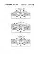
- FIGS. 1-14are cross-sectional, side elevation views illustrating a sequence of process steps in accordance with the present invention.
- FIG. 15is a plan view illustrating one embodiment of the present invention in which the gate electrode is "necked down" as it passed over the active region;
- FIG. 16is a plan view more particularly illustrating one embodiment of the present invention in which the second mask layer is patterned to provide extended metal contacts to the source and drain regions of the device.
- active area 50(as seen in FIG. 1) is formed in a semiconductor substrate 20.
- Active area 50may be formed by conventional isoplanar and etchback methods or by a sidewall or trench isolation process.
- a semiconductor bodysuch as silicon 20
- insultative material 22such as silicon dioxide
- FIG. 1shows active area 50 surrounded by insulative islands 22.
- Semiconductor body 20typically comprises silicon and islands 22 comprise silicon oxide and are typically referred to as the field or field oxide region of the substrate. It is noted that the masking step for the formation of the active area is non-critical, that is, significant alignment and registration problems are not present for this masking operation since it is the first step in the process.
- a first ion implantation mask layer 24is provided.
- a layer of mask materialsuch as silicon nitride is deposited and patterned using a mask which defines the gate pattern. This is the only device gate masking pattern step employed.
- the pattern provided for mask layer 24is substantially the desired pattern for the gate electrode. This pattern typically extends a certain some distance beyond active area 50.
- mask layer 24preferably comprises a material such a silicon nitride, the practice of the present invention is not limited thereto, but may also include any other selectively etchable material such as molybdenum, tungsten, aluminum, polysilicon or silicon oxide. Metals are preferred, but not more preferred than silicon nitride.
- semiconductor body 20is provided with doped regions 28s and 28d forming source and drain regions.
- Doping of semiconductor substrate 20is preferably accomplished by ion implantation. If semiconductor body 20 is doped with P-type dopants, then regions 28s and 28d are preferably doped with N-type dopants. Dopant concentration and ion implant energy levels are chosen to provide a relatively heavy (say N + ) doping for the source and drain rgions. Subsequent doping operations may also optionally be carried out to produce lightly doped source and drain region extensions. These are discussed below.
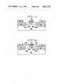
- second ion implantation mask layer 26ais deposited and planarized as shown in FIG. 4.
- Layer 26apreferably comprises a material other than silicon nitride and certainly a material different than that used in first ion implantation mask layer 24.
- this materialmay comprise polycrystalline silicon, metal, or silicon oxide.
- Preferable metalsinclude molybdenum and tungsten or silicides such as tungsten silicide, molybdenum silicide or titanium silicide.
- this materialmay be patterned, as illustrated in FIG. 5, to form metal electrode contacts 26 for the source and drain regions.
- oxide spacer materialis deposited on the sidewalls of layer 26. This deposition is accomplished by low pressure chemical vapor deposition using silane and nitrous oxide. It is noted that formation of oxide spacer material 32 is shown only as being present in the channel region of the FET device being formed. One mechanism for accomplishing this object is delaying the patterning of layer 26a shown in FIG. 4. In such a sequence, spacer oxide material 32 is deposited only in the active area as shown in FIG. 7.
- insultative layer 34is formed by an oxidation process of silicon material 20.
- layer 26comprises metal such as tungsten or molybdenum, then this oxide may be formed using a mixture of hydrogen and water vapor without oxidizing the metal.
- layer 26may comprise a silicide which can be oxidized.
- gate dielectric material 34may be deposited. In either case, the resulting structure is illustrated in FIG. 8.
- gate material 36is deposited and planarized to the surface of layer 26 or slightly below it.
- Gate electrode 26may comprise material such as polycrystalline silicon, molybdenum, or tungsten or silicides such as tantalum silicide or palladium silicide.
- FIG. 9If lightly doped source and drain regions are not desired and if the second mask layer comprises metal, an enhancement mode MOSFET as shown in FIG. 9 can be formed by lateral diffusion of the source and drain dopant under the oxide spacers to form self-aligned junction edges at or slightly underneath the gate edges.
- a functional FETis now present and processing could stop except for covering the device with a passivation layer and interconnecting other devices.
- a depletion mode deviceis already formed since the conductive channel region is already present and gate modulation can be used to either enhance or decrease or "turn off" the channel conductance.
- N-channel enhancement and depletion devicesare formed on the same wafer by providing appropriate dopants in region 28 and by using appropriate masking. For instance, the depletion mode device regions 28 are doped with arsenic (a slow diffuser) and enhancement mode device regions 28 are doped with phosphorous (a fast diffuser).
- oxide spacer material 32is selectively removed and a lightly doped (say N - ) implantation is carried out. Implantation is carried out through gate insulation layer 34 and forms source and drain region extensions 38s and 38d extending from regions 28s and 28d, respectively.
- the dopant concentration and ion implantation energy levelsare selected to produce substantially the dopant distribution illustrated in FIG. 10. in the event that layer 26 comprises metal suitable for use as contact material for source and drain electrodes, a lightly doped transistor structure is complete. However, for purposes of passivation and inclusion of a dielectric layer, oxide material 40a may be redeposited, as shown in FIG. 11.
- Dielectric 40amay be planarized to produce insulative patches 40, as shown in FIG. 12.
- gate electrode material 36can be made thicker and essentially coplanar with the top surfaces of diode contacts 26.
- an interconnectional metal layercan be used to locally interconnect gate pattern 36 with adjacent diode contacts 26. This is advantageous for high packing density in integrated circuits.
- second ion implantation masking layer 26is unsuitable or undesirable as a source or drain electrode contact material
- portions 26 overlying the source and drain regionsmay be selectively etched, resulting in the structure shown in FIG. 13.
- Appropriate source and drain contact material 26'may then be deposited and planarized as necessary. This deposition may be achieved by chemical vapor deposition, but sputtering or by evaporation, again with planarization as needed. The resulting structure is shown in FIG. 14.
- ion implantation mask layer 26comprises metal
- annealing at approximately 650° C. or flash annealingmay be used to anneal the lightly doped implant.
- material 26comprises a metal silicide
- normal thermal sinteringis used since no reaction can take place with the underlying silicon material.
- regions 28s and 28dare N + -doped and regions 38s and N - -doped regions to make N-channel devices.
- opposite polarity dopantsare employed to make P-channel devices.
- CMOS devicesare fabricated by appropriate ion implantation and masking during source and drain doping of regions 28 and 38.
- the process described hereinis well adapted to conventional VLSI processing and fabrication. It is also seen that the process described herein is particularly advantageous in that few masking steps are required and that none of these masking steps is critical. It is also seen that the process is particularly advantageous in that the secondion implantation mask layer also may be employed as a layer which constitutes the source and drain contacts. Source and drain contacts are therefore substantially aligned with the silicon diodes and no further masking or patterning is required to form these contacts. This makes it possible to considerably reduce the device diode areas which enhances the speed and performance characteristics of FET devices by reduction of the parasitic diode capacitances. It is also seen that the gate material may be deposited not only to provide a pad for gate electrode contact, but also to provide an extremely narrow gate electrode resulting in a desirably narrow or short channel length for FET devices.
Landscapes
- Physics & Mathematics (AREA)
- High Energy & Nuclear Physics (AREA)
- Engineering & Computer Science (AREA)
- Health & Medical Sciences (AREA)
- Toxicology (AREA)
- Condensed Matter Physics & Semiconductors (AREA)
- General Physics & Mathematics (AREA)
- Manufacturing & Machinery (AREA)
- Computer Hardware Design (AREA)
- Microelectronics & Electronic Packaging (AREA)
- Power Engineering (AREA)
- Insulated Gate Type Field-Effect Transistor (AREA)
Abstract
Description
Claims (31)
Priority Applications (1)
| Application Number | Priority Date | Filing Date | Title |
|---|---|---|---|
| US06/853,108US4677736A (en) | 1986-04-17 | 1986-04-17 | Self-aligned inlay transistor with or without source and drain self-aligned metallization extensions |
Applications Claiming Priority (1)
| Application Number | Priority Date | Filing Date | Title |
|---|---|---|---|
| US06/853,108US4677736A (en) | 1986-04-17 | 1986-04-17 | Self-aligned inlay transistor with or without source and drain self-aligned metallization extensions |
Publications (1)
| Publication Number | Publication Date |
|---|---|
| US4677736Atrue US4677736A (en) | 1987-07-07 |
Family
ID=25315076
Family Applications (1)
| Application Number | Title | Priority Date | Filing Date |
|---|---|---|---|
| US06/853,108Expired - LifetimeUS4677736A (en) | 1986-04-17 | 1986-04-17 | Self-aligned inlay transistor with or without source and drain self-aligned metallization extensions |
Country Status (1)
| Country | Link |
|---|---|
| US (1) | US4677736A (en) |
Cited By (19)
| Publication number | Priority date | Publication date | Assignee | Title |
|---|---|---|---|---|
| US4803173A (en)* | 1987-06-29 | 1989-02-07 | North American Philips Corporation, Signetics Division | Method of fabrication of semiconductor device having a planar configuration |
| US4944682A (en)* | 1988-10-07 | 1990-07-31 | International Business Machines Corporation | Method of forming borderless contacts |
| US4965219A (en)* | 1984-07-19 | 1990-10-23 | Sgs Microelettronica Spa | Method for the manufacturing of insulated gate field effect transistors (IGFETS) having a high response speed in high density integrated circuits |
| US5079180A (en)* | 1988-12-22 | 1992-01-07 | Texas Instruments Incorporated | Method of fabricating a raised source/drain transistor |
| US5124272A (en)* | 1989-08-11 | 1992-06-23 | Seiko Instruments, Inc. | Method of producing field effect transistor |
| EP0495541A1 (en)* | 1991-01-16 | 1992-07-22 | Koninklijke Philips Electronics N.V. | Method of manufacturing a semiconductor device provided with a field effect transistor |
| EP0495650A3 (en)* | 1991-01-16 | 1993-05-12 | Sharp Kabushiki Kaisha | Method of fabricating field-effect transistor |
| US5422289A (en)* | 1992-04-27 | 1995-06-06 | National Semiconductor Corporation | Method of manufacturing a fully planarized MOSFET and resulting structure |
| US5532185A (en)* | 1991-03-27 | 1996-07-02 | Seiko Instruments Inc. | Impurity doping method with adsorbed diffusion source |
| US5654241A (en)* | 1988-12-23 | 1997-08-05 | Kabushiki Kaisha Toshiba | Method for manufacturing a semiconductor device having reduced resistance of diffusion layers and gate electrodes |
| US6002152A (en)* | 1992-01-14 | 1999-12-14 | Sandisk Corporation | EEPROM with split gate source side injection with sidewall spacers |
| US6140190A (en)* | 1997-12-18 | 2000-10-31 | Advanced Micro Devices | Method and structure for elevated source/drain with polished gate electrode insulated gate field effect transistors |
| US6222762B1 (en) | 1992-01-14 | 2001-04-24 | Sandisk Corporation | Multi-state memory |
| US6265256B1 (en)* | 1998-09-17 | 2001-07-24 | Advanced Micro Devices, Inc. | MOS transistor with minimal overlap between gate and source/drain extensions |
| US6432317B1 (en)* | 1991-02-28 | 2002-08-13 | Texas Instruments Incorporated | Method to produce masking |
| US6472274B1 (en)* | 2000-06-29 | 2002-10-29 | International Business Machines Corporation | MOSFET with self-aligned channel edge implant and method |
| US20030052360A1 (en)* | 1992-01-14 | 2003-03-20 | Guterman Daniel C. | EEPROM with split gate source side injection with sidewall spacers |
| US20040137688A1 (en)* | 1999-10-07 | 2004-07-15 | Chorng-Ping Chang | Semiconductor device with tapered gate and process for fabricating the device |
| US20050184343A1 (en)* | 1999-06-02 | 2005-08-25 | Thornton Trevor J. | MESFETs integrated with MOSFETs on common substrate and methods of forming the same |
Citations (5)
| Publication number | Priority date | Publication date | Assignee | Title |
|---|---|---|---|---|
| US4419810A (en)* | 1981-12-30 | 1983-12-13 | International Business Machines Corporation | Self-aligned field effect transistor process |
| US4472872A (en)* | 1982-12-21 | 1984-09-25 | Tokyo Shibaura Denki Kabushiki Kaisha | Method of fabricating a Schottky gate field effect transistor |
| US4536782A (en)* | 1983-09-22 | 1985-08-20 | General Electric Company | Field effect semiconductor devices and method of making same |
| US4577392A (en)* | 1984-08-03 | 1986-03-25 | Advanced Micro Devices, Inc. | Fabrication technique for integrated circuits |
| US4599789A (en)* | 1984-06-15 | 1986-07-15 | Harris Corporation | Process of making twin well VLSI CMOS |
- 1986
- 1986-04-17USUS06/853,108patent/US4677736A/ennot_activeExpired - Lifetime
Patent Citations (5)
| Publication number | Priority date | Publication date | Assignee | Title |
|---|---|---|---|---|
| US4419810A (en)* | 1981-12-30 | 1983-12-13 | International Business Machines Corporation | Self-aligned field effect transistor process |
| US4472872A (en)* | 1982-12-21 | 1984-09-25 | Tokyo Shibaura Denki Kabushiki Kaisha | Method of fabricating a Schottky gate field effect transistor |
| US4536782A (en)* | 1983-09-22 | 1985-08-20 | General Electric Company | Field effect semiconductor devices and method of making same |
| US4599789A (en)* | 1984-06-15 | 1986-07-15 | Harris Corporation | Process of making twin well VLSI CMOS |
| US4577392A (en)* | 1984-08-03 | 1986-03-25 | Advanced Micro Devices, Inc. | Fabrication technique for integrated circuits |
Non-Patent Citations (2)
| Title |
|---|
| Bassous et al., "Self-Aligned Polysilicon Gate MOSFETs with Tailored Source and Drain Profiles", IBM Tech. Dis. Bulletin, vol. 22, No. 11, Apr. 1980. |
| Bassous et al., Self Aligned Polysilicon Gate MOSFETs with Tailored Source and Drain Profiles , IBM Tech. Dis. Bulletin, vol. 22, No. 11, Apr. 1980.* |
Cited By (50)
| Publication number | Priority date | Publication date | Assignee | Title |
|---|---|---|---|---|
| US4965219A (en)* | 1984-07-19 | 1990-10-23 | Sgs Microelettronica Spa | Method for the manufacturing of insulated gate field effect transistors (IGFETS) having a high response speed in high density integrated circuits |
| US4803173A (en)* | 1987-06-29 | 1989-02-07 | North American Philips Corporation, Signetics Division | Method of fabrication of semiconductor device having a planar configuration |
| US4944682A (en)* | 1988-10-07 | 1990-07-31 | International Business Machines Corporation | Method of forming borderless contacts |
| US5079180A (en)* | 1988-12-22 | 1992-01-07 | Texas Instruments Incorporated | Method of fabricating a raised source/drain transistor |
| US5654241A (en)* | 1988-12-23 | 1997-08-05 | Kabushiki Kaisha Toshiba | Method for manufacturing a semiconductor device having reduced resistance of diffusion layers and gate electrodes |
| US5124272A (en)* | 1989-08-11 | 1992-06-23 | Seiko Instruments, Inc. | Method of producing field effect transistor |
| EP0495541A1 (en)* | 1991-01-16 | 1992-07-22 | Koninklijke Philips Electronics N.V. | Method of manufacturing a semiconductor device provided with a field effect transistor |
| EP0495650A3 (en)* | 1991-01-16 | 1993-05-12 | Sharp Kabushiki Kaisha | Method of fabricating field-effect transistor |
| US6432317B1 (en)* | 1991-02-28 | 2002-08-13 | Texas Instruments Incorporated | Method to produce masking |
| US5532185A (en)* | 1991-03-27 | 1996-07-02 | Seiko Instruments Inc. | Impurity doping method with adsorbed diffusion source |
| US6222762B1 (en) | 1992-01-14 | 2001-04-24 | Sandisk Corporation | Multi-state memory |
| US20030052360A1 (en)* | 1992-01-14 | 2003-03-20 | Guterman Daniel C. | EEPROM with split gate source side injection with sidewall spacers |
| US6856546B2 (en) | 1992-01-14 | 2005-02-15 | Sandisk Corporation | Multi-state memory |
| US6954381B2 (en) | 1992-01-14 | 2005-10-11 | Sandisk Corporation | EEPROM with split gate source side injection with sidewall spacers |
| US6275419B1 (en) | 1992-01-14 | 2001-08-14 | Sandisk Corporation | Multi-state memory |
| US6317364B1 (en) | 1992-01-14 | 2001-11-13 | Sandisk Corporation | Multi-state memory |
| US6317363B1 (en) | 1992-01-14 | 2001-11-13 | Sandisk Corporation | Multi-state memory |
| US6002152A (en)* | 1992-01-14 | 1999-12-14 | Sandisk Corporation | EEPROM with split gate source side injection with sidewall spacers |
| US7898868B2 (en) | 1992-01-14 | 2011-03-01 | Sandisk Corporation | Multi-state memory |
| US5422289A (en)* | 1992-04-27 | 1995-06-06 | National Semiconductor Corporation | Method of manufacturing a fully planarized MOSFET and resulting structure |
| US20060163645A1 (en)* | 1996-02-28 | 2006-07-27 | Guterman Daniel C | EEPROM With Split Gate Source Side Injection |
| US6664587B2 (en) | 1996-02-28 | 2003-12-16 | Sandisk Corporation | EEPROM cell array structure with specific floating gate shape |
| US7071060B1 (en) | 1996-02-28 | 2006-07-04 | Sandisk Corporation | EEPROM with split gate source side infection with sidewall spacers |
| US6704222B2 (en) | 1996-02-28 | 2004-03-09 | Sandisk Corporation | Multi-state operation of dual floating gate array |
| US20040063283A1 (en)* | 1996-02-28 | 2004-04-01 | Guterman Daniel C. | Eeprom with split gate source side injection |
| US7449746B2 (en) | 1996-02-28 | 2008-11-11 | Sandisk Corporation | EEPROM with split gate source side injection |
| US6861700B2 (en) | 1996-02-28 | 2005-03-01 | Sandisk Corporation | Eeprom with split gate source side injection |
| US20040165431A1 (en)* | 1997-08-07 | 2004-08-26 | Guterman Daniel C. | Novel multi-state memory |
| US20080212374A1 (en)* | 1997-08-07 | 2008-09-04 | Guterman Daniel C | Novel Multi-State Memory |
| US7573740B2 (en) | 1997-08-07 | 2009-08-11 | Sandisk Corporation | Multi-state memory |
| US6894926B2 (en) | 1997-08-07 | 2005-05-17 | Sandisk Corporation | Multi-state memory |
| US20050180211A1 (en)* | 1997-08-07 | 2005-08-18 | Guterman Daniel C. | Novel multi-state memory |
| US7457162B2 (en) | 1997-08-07 | 2008-11-25 | Sandisk Corporation | Multi-state memory |
| US7443723B2 (en) | 1997-08-07 | 2008-10-28 | Sandisk Corporation | Multi-state memory |
| US20060034124A1 (en)* | 1997-08-07 | 2006-02-16 | Sandisk Corporation | Novel multi-state memory |
| US20060129751A1 (en)* | 1997-08-07 | 2006-06-15 | Guterman Daniel C | Novel multi-state memory |
| US20040042294A1 (en)* | 1997-08-07 | 2004-03-04 | Guterman Daniel C. | Novel Multi-state memory |
| US6862218B2 (en) | 1997-08-07 | 2005-03-01 | Sandisk Corporation | Multi-state memory |
| US7088615B2 (en) | 1997-08-07 | 2006-08-08 | Sandisk Corporation | Multi-state memory |
| US7187592B2 (en) | 1997-08-07 | 2007-03-06 | Sandisk Corporation | Multi-state memory |
| US7289360B2 (en) | 1997-08-07 | 2007-10-30 | Sandisk Corporation | Multi-state memory |
| US7345934B2 (en) | 1997-08-07 | 2008-03-18 | Sandisk Corporation | Multi-state memory |
| US7385843B2 (en) | 1997-08-07 | 2008-06-10 | Sandisk Corporation | Multi-state memory |
| US6140190A (en)* | 1997-12-18 | 2000-10-31 | Advanced Micro Devices | Method and structure for elevated source/drain with polished gate electrode insulated gate field effect transistors |
| US6265256B1 (en)* | 1998-09-17 | 2001-07-24 | Advanced Micro Devices, Inc. | MOS transistor with minimal overlap between gate and source/drain extensions |
| US20050184343A1 (en)* | 1999-06-02 | 2005-08-25 | Thornton Trevor J. | MESFETs integrated with MOSFETs on common substrate and methods of forming the same |
| US7589007B2 (en)* | 1999-06-02 | 2009-09-15 | Arizona Board Of Regents For And On Behalf Of Arizona State University | MESFETs integrated with MOSFETs on common substrate and methods of forming the same |
| US20040137688A1 (en)* | 1999-10-07 | 2004-07-15 | Chorng-Ping Chang | Semiconductor device with tapered gate and process for fabricating the device |
| EP1091414A3 (en)* | 1999-10-07 | 2005-03-16 | Lucent Technologies Inc. | MOSFET with tapered gate and method of manufacturing it |
| US6472274B1 (en)* | 2000-06-29 | 2002-10-29 | International Business Machines Corporation | MOSFET with self-aligned channel edge implant and method |
Similar Documents
| Publication | Publication Date | Title |
|---|---|---|
| US4677736A (en) | Self-aligned inlay transistor with or without source and drain self-aligned metallization extensions | |
| US5472897A (en) | Method for fabricating MOS device with reduced anti-punchthrough region | |
| EP0074215B1 (en) | Cmos devices with self-aligned channel stops | |
| US5108937A (en) | Method of making a recessed gate MOSFET device structure | |
| US6124189A (en) | Metallization structure and method for a semiconductor device | |
| US4149307A (en) | Process for fabricating insulated-gate field-effect transistors with self-aligned contacts | |
| EP0083785A2 (en) | Method of forming self-aligned field effect transistors in integrated circuit structures | |
| US5294822A (en) | Polycide local interconnect method and structure | |
| US4663825A (en) | Method of manufacturing semiconductor device | |
| US5198378A (en) | Process of fabricating elevated source/drain transistor | |
| US5286663A (en) | Methods for producing thin film transistor having a diode shunt | |
| US5202277A (en) | Method of fabricating a semiconductor device | |
| US4717689A (en) | Method of forming semimicron grooves in semiconductor material | |
| US6664150B2 (en) | Active well schemes for SOI technology | |
| US5213990A (en) | Method for forming a stacked semiconductor structure | |
| US5814541A (en) | Method for manufacturing semiconductor device | |
| US6146978A (en) | Integrated circuit having an interlevel interconnect coupled to a source/drain region(s) with source/drain region(s) boundary overlap and reduced parasitic capacitance | |
| JP4491858B2 (en) | Manufacturing method of semiconductor device | |
| US4517731A (en) | Double polysilicon process for fabricating CMOS integrated circuits | |
| US6995055B2 (en) | Structure of a semiconductor integrated circuit and method of manufacturing the same | |
| US5924001A (en) | Ion implantation for preventing polycide void | |
| US5612243A (en) | Polycide local interconnect method and structure | |
| US5670417A (en) | Method for fabricating self-aligned semiconductor component | |
| US4826779A (en) | Integrated capacitor and method of fabricating same | |
| US5773344A (en) | Semiconductor device having gate electrode and impurity diffusion layer different in conductivity type and method of manufacturing same |
Legal Events
| Date | Code | Title | Description |
|---|---|---|---|
| AS | Assignment | Owner name:GENERAL ELECTRIC COMPANY, A CORP OF N.Y. Free format text:ASSIGNMENT OF ASSIGNORS INTEREST.;ASSIGNOR:BROWN, DALE M.;REEL/FRAME:004551/0135 Effective date:19860411 Owner name:GENERAL ELECTRIC COMPANY, NEW YORK Free format text:ASSIGNMENT OF ASSIGNORS INTEREST;ASSIGNOR:BROWN, DALE M.;REEL/FRAME:004551/0135 Effective date:19860411 | |
| FEPP | Fee payment procedure | Free format text:PAYOR NUMBER ASSIGNED (ORIGINAL EVENT CODE: ASPN); ENTITY STATUS OF PATENT OWNER: LARGE ENTITY | |
| STCF | Information on status: patent grant | Free format text:PATENTED CASE | |
| FPAY | Fee payment | Year of fee payment:4 | |
| FEPP | Fee payment procedure | Free format text:PAYOR NUMBER ASSIGNED (ORIGINAL EVENT CODE: ASPN); ENTITY STATUS OF PATENT OWNER: LARGE ENTITY Free format text:PAYER NUMBER DE-ASSIGNED (ORIGINAL EVENT CODE: RMPN); ENTITY STATUS OF PATENT OWNER: LARGE ENTITY | |
| FPAY | Fee payment | Year of fee payment:8 | |
| REMI | Maintenance fee reminder mailed | ||
| FPAY | Fee payment | Year of fee payment:12 | |
| REMI | Maintenance fee reminder mailed | ||
| AS | Assignment | Owner name:INTERSIL CORPORATION, FLORIDA Free format text:ASSIGNMENT OF ASSIGNORS INTEREST;ASSIGNOR:HARRIS CORPORATION;REEL/FRAME:010255/0405 Effective date:19990813 | |
| AS | Assignment | Owner name:CREDIT SUISSE FIRST BOSTON, AS COLLATERAL AGENT, N Free format text:SECURITY INTEREST;ASSIGNOR:INTERSIL CORPORATION;REEL/FRAME:010351/0410 Effective date:19990813 |