US4674320A - Chemoresistive gas sensor - Google Patents
Chemoresistive gas sensorDownload PDFInfo
- Publication number
- US4674320A US4674320AUS06/781,543US78154385AUS4674320AUS 4674320 AUS4674320 AUS 4674320AUS 78154385 AUS78154385 AUS 78154385AUS 4674320 AUS4674320 AUS 4674320A
- Authority
- US
- United States
- Prior art keywords
- layer
- organic semiconductor
- high conductivity
- conductivity material
- islands
- Prior art date
- Legal status (The legal status is an assumption and is not a legal conclusion. Google has not performed a legal analysis and makes no representation as to the accuracy of the status listed.)
- Expired - Fee Related
Links
- 239000000463materialSubstances0.000claimsabstractdescription41
- 239000004065semiconductorSubstances0.000claimsabstractdescription39
- 239000000356contaminantSubstances0.000claimsabstractdescription15
- 230000005641tunnelingEffects0.000claimsabstractdescription6
- 239000000758substrateSubstances0.000claimsdescription23
- 238000000034methodMethods0.000claimsdescription9
- IEQIEDJGQAUEQZ-UHFFFAOYSA-NphthalocyanineChemical groupN1C(N=C2C3=CC=CC=C3C(N=C3C4=CC=CC=C4C(=N4)N3)=N2)=C(C=CC=C2)C2=C1N=C1C2=CC=CC=C2C4=N1IEQIEDJGQAUEQZ-UHFFFAOYSA-N0.000claimsdescription9
- PCHJSUWPFVWCPO-UHFFFAOYSA-NgoldChemical compound[Au]PCHJSUWPFVWCPO-UHFFFAOYSA-N0.000claimsdescription4
- 239000010931goldSubstances0.000claimsdescription4
- 229910052737goldInorganic materials0.000claimsdescription4
- 238000000151depositionMethods0.000claimsdescription3
- 238000001816coolingMethods0.000claimsdescription2
- 229910052594sapphireInorganic materials0.000claimsdescription2
- 239000010980sapphireSubstances0.000claimsdescription2
- 238000010438heat treatmentMethods0.000claims2
- 230000035945sensitivityEffects0.000abstractdescription7
- 238000001179sorption measurementMethods0.000abstractdescription2
- 239000002245particleSubstances0.000abstract1
- 239000010410layerSubstances0.000description26
- 239000007789gasSubstances0.000description14
- 239000003463adsorbentSubstances0.000description4
- 239000010409thin filmSubstances0.000description4
- 238000013459approachMethods0.000description3
- 230000015572biosynthetic processEffects0.000description3
- 238000000576coating methodMethods0.000description2
- 239000013078crystalSubstances0.000description2
- 238000001514detection methodMethods0.000description2
- 239000003344environmental pollutantSubstances0.000description2
- 239000010408filmSubstances0.000description2
- 238000012986modificationMethods0.000description2
- 230000004048modificationEffects0.000description2
- 238000012544monitoring processMethods0.000description2
- 229920000642polymerPolymers0.000description2
- 230000004044responseEffects0.000description2
- 241001550206CollaSpecies0.000description1
- HSFWRNGVRCDJHI-UHFFFAOYSA-Nalpha-acetyleneNatural productsC#CHSFWRNGVRCDJHI-UHFFFAOYSA-N0.000description1
- 239000003994anesthetic gasSubstances0.000description1
- 230000008859changeEffects0.000description1
- 239000002575chemical warfare agentSubstances0.000description1
- 239000011248coating agentSubstances0.000description1
- 239000004020conductorSubstances0.000description1
- 239000000470constituentSubstances0.000description1
- 230000001419dependent effectEffects0.000description1
- 230000000694effectsEffects0.000description1
- 230000002708enhancing effectEffects0.000description1
- 125000002534ethynyl groupChemical group[H]C#C*0.000description1
- 238000000556factor analysisMethods0.000description1
- 238000009501film coatingMethods0.000description1
- 239000012535impuritySubstances0.000description1
- 238000001465metallisationMethods0.000description1
- 230000037361pathwayEffects0.000description1
- 231100000719pollutantToxicity0.000description1
- 238000003825pressingMethods0.000description1
- 238000000746purificationMethods0.000description1
- 239000010453quartzSubstances0.000description1
- 238000012552reviewMethods0.000description1
- VYPSYNLAJGMNEJ-UHFFFAOYSA-Nsilicon dioxideInorganic materialsO=[Si]=OVYPSYNLAJGMNEJ-UHFFFAOYSA-N0.000description1
- 239000002356single layerSubstances0.000description1
- 238000000859sublimationMethods0.000description1
- 230000008022sublimationEffects0.000description1
- 238000012360testing methodMethods0.000description1
Images
Classifications
- G—PHYSICS
- G01—MEASURING; TESTING
- G01N—INVESTIGATING OR ANALYSING MATERIALS BY DETERMINING THEIR CHEMICAL OR PHYSICAL PROPERTIES
- G01N27/00—Investigating or analysing materials by the use of electric, electrochemical, or magnetic means
- G01N27/02—Investigating or analysing materials by the use of electric, electrochemical, or magnetic means by investigating impedance
- G01N27/04—Investigating or analysing materials by the use of electric, electrochemical, or magnetic means by investigating impedance by investigating resistance
- G01N27/12—Investigating or analysing materials by the use of electric, electrochemical, or magnetic means by investigating impedance by investigating resistance of a solid body in dependence upon absorption of a fluid; of a solid body in dependence upon reaction with a fluid, for detecting components in the fluid
- G01N27/125—Composition of the body, e.g. the composition of its sensitive layer
- G01N27/126—Composition of the body, e.g. the composition of its sensitive layer comprising organic polymers
Definitions
- the inventionrelates generally to gas sensing apparatus, and more particularly to gas sensing apparatus utilizing the adsorbent properties of organic semiconductors.
- the selectivity of individual piezoelectric sorption detectors of the type disclosed by King, Jr., U.S. Pat. Nos. 3,164,004 or by Frechette et al, 4,111,036,depends entirely on the selectivity of the adsorbent coatings on the piezoelectric crystals.
- the selectivity of these adsorbent materialsare notoriously poor, e.g., Hirschfeld, "Providing Innovative System Monitoring and Reliability Assessment Through Microengineering", Energy Technology and Review, February 1984; and Edwards et al, "A Quartz Crystal Piezoelectric Device for Monitoring Organic Gaseous Pollutants", Analytica Chimica Acta, Vol.
- Selectivity problemscan be overcome to a large extent by employing a plurality of sensors each having a different adsorbent coating.
- the responses of the multiple sensorsare analyzed by factor analysis or least squares analysis to obtain information about the concentrations of contaminants in the gas being monitored.
- chemoresistive gas sensorsAnother approach to detecting contaminant gases utilizes their effects on the conductivities of certain organic semiconductors.
- the class of sensors based on this approachis referred to as chemoresistive gas sensors.
- a thin layer of organic semiconductoris disposed on a surface between two electrodes. The layer of organic semiconductor is exposed to the atmosphere containing the contaminant gases of interest. As the organic semiconductor adsorbs the contaminant gases, its conductivity changes, and the magnitude of the change is related to the concentration of contaminant gas.
- the following referencesprovide representative disclosures of such gas detection systems: Colla et al, U.S. Pat. Nos.
- This class of sensoris also limited by the extremely low conductivity of the layers of organic semiconductor, which is on the order of 10 -10 -10 -8 ohms -1 .
- the low conductivitymeans that the changes introduced by the adsorbed contaminants will be correspondingly low and difficult to detect; hence, the sensitivity of the system is low.
- An object of the inventionis to provide a sensor for gaseous contaminants with improved selectivity and sensitivity.
- Another object of the inventionis to improve the sensitivity of chemoresistive gas sensors.
- the layer of organic semiconductor together with the embedded islands of high conductive materialis placed on a nonconductive substrate having good thermal conductivity.
- Good thermal conductivityallows the temperature of the layer of organic semiconductor to be controlled so that temperature-dependent changes in conductivity can be eliminated, or minimized.
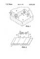
- FIG. 1is a cutaway view of the layer of organic semiconductor on a substrate that exposes the islands of high conductivity material
- FIG. 2is an illustration of an embodiment of the invention employing a single layer of organic semiconductor.
- the inventionis a chemoresistive gas sensor with increased sensitivity, and method for making same.
- the increased sensitivityis attained by modifying a layer of organic semiconductor so that it contains islands of high conductivity material.
- the average interisland spacingis selected so that the predominant current path through the layer is by way of electron tunneling between the islands.
- the presence of the islands in accordance with the inventionincreases the conductivity of the chemosensitive layer by two to three orders of magnitude, and thereby causes corresponding increases in the variances in current due to gaseous contaminants being adsorbed onto or expelled from the layer of organic semiconductor.
- FIG. 1presents a cutaway view of a layer of organic semiconductor which illustrates how the islands of high conductivity material are embedded in the layer.
- islands 10 of high conductivity materialare covered by and embedded in organic semiconductor 12 to form chemoresistive layer 14 on substrate 16.
- FIG. 2illustrates an embodiment of the invention employing a single kind of organic semiconductor.
- Chemoresistive layer 14is disposed between electrodes 20 and 22 on substrate 16. Electrodes 20 and 22 are connected to voltage source 24 by leads 26 and 28. The current passing through the chemoresistive layer is monitored by meter 30.
- a critical parameter of the chemoresistive layeris the average interisland spacing of high conductivity material.
- the average interisland spacingis between about 10-80 Angstroms. Most preferably, the average interisland spacing is between about 50-60 Angstroms.
- organic semiconductorsare suitable for use with the present invention including phthalocyanine and its derivatives (disclosed in Moser et al, in Phthalocyanine Compounds (Van Nostrand, New York, 1963); electrically conductive acetylene polymers (disclosed in U.S. Pat. Nos. 4,510,075 and 4,510,076); polymeric semiconductors disclosed in U.S. Pat. No. 4,472,356; and the like.
- the three cited U.S. patentsare incorporated by reference to their disclosures of organic semiconductors.
- the preferred organic semiconductoris phthalocyanine and its derivatives, particularly its halogenated or sulfonated derivatives.
- the substrate to which the chemoresistive layer is attachedis nonconductive electrically, but preferably it has good heat conductivity.
- a preferred substrate materialis sapphire.
- the preferred embodiment of the inventionis constructed by depositing a continuous thin film of high conductivity material on the substrate surface between electrodes 20 and 22.
- the high conductivity materialis gold.
- the thin filmis preferably between about 100-300 Angstroms thick, and is deposited by standard metal deposition techniques.
- the substrate material with the continuous thin film coatingis then heated to a temperature high enough for the thin film to form mobile droplets on the surface of the substrate. At this temperature, the droplets move around on the surface of the substrate and coalesce when they come into contact with one another. when the droplets cool and solidify, they form the islands of high conductivity material. By maintaining the substrate at the elevated temperature, one can adjust the average interisland spacing.
- the surface of the substrate on which the chemoresistive layer restsis optically smooth. That is, it is smooth enough so that droplet formation occurs, and there are no sizable grooves, cracks, or other irregularities which could cause the formation of channels of high conductivity material upon cooling. Such a condition is undesirable because the channels would provide alternative current pathways to electron tunneling.
- the preferred temperature for formation of dropletsis between about 150°-200° C.
- the organic semiconductoris deposited on the solidified islands by sublimation under a vacuum in order to avoid impurities in the chemoresistive layer, e.g., by the method disclosed by Bott et all, Sensors and Actuators, Vol. 5, pgs. 43-53 (1984), or like method.
- the thickness of the layer of organic semiconductoris on the order of the average diameter of the islands of high conductivity material. Thicker layers reduce the response time of the sensor; thinner layers may in.troduce undesirable complications because of inhomogeneities in the material between islands.
Landscapes
- Chemical & Material Sciences (AREA)
- Chemical Kinetics & Catalysis (AREA)
- Electrochemistry (AREA)
- Physics & Mathematics (AREA)
- Health & Medical Sciences (AREA)
- Life Sciences & Earth Sciences (AREA)
- Analytical Chemistry (AREA)
- Biochemistry (AREA)
- General Health & Medical Sciences (AREA)
- General Physics & Mathematics (AREA)
- Immunology (AREA)
- Pathology (AREA)
- Investigating Or Analyzing Materials By The Use Of Fluid Adsorption Or Reactions (AREA)
Abstract
Description
The U.S. Government has rights in this invention pursuant to Contract No. W-7405-ENG-48 between the U.S. Department of Energy and the University of California, for the operation of the Lawrence Livermore National Laboratory.
The invention relates generally to gas sensing apparatus, and more particularly to gas sensing apparatus utilizing the adsorbent properties of organic semiconductors.
There is pressing need for highly selective and sensitive detectors of gaseous constituents in a wide variety of industrial, medical, and military contexts. There is a need to detect and monitor contaminant gases in industrial purification processes; anesthetic gases in operating rooms; chemical warfare agents on the battlefields; and environmental pollutants in industrial or agricultural areas.
Many of the current approaches to contaminant gas detection lack sensitivity and selectivity. For example, the selectivity of individual piezoelectric sorption detectors of the type disclosed by King, Jr., U.S. Pat. Nos. 3,164,004 or by Frechette et al, 4,111,036, depends entirely on the selectivity of the adsorbent coatings on the piezoelectric crystals. The selectivity of these adsorbent materials are notoriously poor, e.g., Hirschfeld, "Providing Innovative System Monitoring and Reliability Assessment Through Microengineering", Energy Technology and Review, February 1984; and Edwards et al, "A Quartz Crystal Piezoelectric Device for Monitoring Organic Gaseous Pollutants", Analytica Chimica Acta, Vol. 117, pgs. 147-157 (1980). Selectivity problems can be overcome to a large extent by employing a plurality of sensors each having a different adsorbent coating. The responses of the multiple sensors are analyzed by factor analysis or least squares analysis to obtain information about the concentrations of contaminants in the gas being monitored.
Another approach to detecting contaminant gases utilizes their effects on the conductivities of certain organic semiconductors. The class of sensors based on this approach is referred to as chemoresistive gas sensors. A thin layer of organic semiconductor is disposed on a surface between two electrodes. The layer of organic semiconductor is exposed to the atmosphere containing the contaminant gases of interest. As the organic semiconductor adsorbs the contaminant gases, its conductivity changes, and the magnitude of the change is related to the concentration of contaminant gas. The following references provide representative disclosures of such gas detection systems: Colla et al, U.S. Pat. Nos. 4,142,400 and 4,236,307; Kolesar, 4,472,356; Bott et al, "A Highly Sensitive NO2 Sensor Based on Electrical Conductivity Changes in Phthalocyanine Films", Sensors and Actuators, Vol. 5, pgs. 43-53 (1984); and Hermans, "CO, CO2, CH4, and H2 O Sensing by Polymer Covered Interdigitating Electrode Structures", Sensors and Actuators, Vol. 5, pgs. 181-186 (1984). Like the piezoelectric-based sensors, the selectivity of chemoresistive sensors is limited by the lack of selectivity of the organic semiconductors for particular gaseous contaminants. This class of sensor is also limited by the extremely low conductivity of the layers of organic semiconductor, which is on the order of 10-10 -10-8 ohms-1. The low conductivity means that the changes introduced by the adsorbed contaminants will be correspondingly low and difficult to detect; hence, the sensitivity of the system is low.
An object of the invention is to provide a sensor for gaseous contaminants with improved selectivity and sensitivity.
Another object of the invention is to improve the sensitivity of chemoresistive gas sensors.
Additional objects, advantages and novel features of the invention will be set forth in part in the description which follows, and in part will become apparent to those skilled in the art upon examination of the following or may be learned by practice of the invention. The objects and advantages of the invention may be realized and attained by means of the instrumentalities and combinations particularly pointed out in the appended claims.
These and other objects are attained in accordance with the present invention by enhancing the conductivity of the organic semiconductor layers used in chemoresistive gas sensors. Chemically inert, high conductivity materials are embedded in the organic semiconductor layer such that islands of high conductivity material are dispersed throughout the layer at a predetermined average interisland spacing. The average interisland spacing is selected so that the predominant path of current flow is by way of electron tunneling between the islands of high conductivity material. The magnitude of the tunneling current depends on the nature of the high conductivity material, the nature of the organic semiconductor, the average distance between the islands of high conductivity material, the average size of the islands, the voltage across the layer of organic semiconductor, and the amount of gaseous contaminants adsorbed onto the organic semiconductor. In accordance with the invention, all of the above factors are predetermined, except the amount of gaseous contaminants adsorbed onto the organic semiconductor.
Preferably, the layer of organic semiconductor together with the embedded islands of high conductive material is placed on a nonconductive substrate having good thermal conductivity. Good thermal conductivity allows the temperature of the layer of organic semiconductor to be controlled so that temperature-dependent changes in conductivity can be eliminated, or minimized.
FIG. 1 is a cutaway view of the layer of organic semiconductor on a substrate that exposes the islands of high conductivity material; and
FIG. 2 is an illustration of an embodiment of the invention employing a single layer of organic semiconductor.
The invention is a chemoresistive gas sensor with increased sensitivity, and method for making same. The increased sensitivity is attained by modifying a layer of organic semiconductor so that it contains islands of high conductivity material. The average interisland spacing is selected so that the predominant current path through the layer is by way of electron tunneling between the islands. The presence of the islands in accordance with the invention increases the conductivity of the chemosensitive layer by two to three orders of magnitude, and thereby causes corresponding increases in the variances in current due to gaseous contaminants being adsorbed onto or expelled from the layer of organic semiconductor.
FIG. 1 presents a cutaway view of a layer of organic semiconductor which illustrates how the islands of high conductivity material are embedded in the layer. In this embodiment,islands 10 of high conductivity material are covered by and embedded inorganic semiconductor 12 to formchemoresistive layer 14 onsubstrate 16.
FIG. 2 illustrates an embodiment of the invention employing a single kind of organic semiconductor.Chemoresistive layer 14 is disposed betweenelectrodes 20 and 22 onsubstrate 16.Electrodes 20 and 22 are connected to voltage source 24 byleads meter 30.
A critical parameter of the chemoresistive layer is the average interisland spacing of high conductivity material. Preferably, the average interisland spacing is between about 10-80 Angstroms. Most preferably, the average interisland spacing is between about 50-60 Angstroms.
Several organic semiconductors are suitable for use with the present invention including phthalocyanine and its derivatives (disclosed in Moser et al, in Phthalocyanine Compounds (Van Nostrand, New York, 1963); electrically conductive acetylene polymers (disclosed in U.S. Pat. Nos. 4,510,075 and 4,510,076); polymeric semiconductors disclosed in U.S. Pat. No. 4,472,356; and the like. The three cited U.S. patents are incorporated by reference to their disclosures of organic semiconductors. The preferred organic semiconductor is phthalocyanine and its derivatives, particularly its halogenated or sulfonated derivatives.
The substrate to which the chemoresistive layer is attached is nonconductive electrically, but preferably it has good heat conductivity. A preferred substrate material is sapphire.
Referring to FIG. 2, the preferred embodiment of the invention is constructed by depositing a continuous thin film of high conductivity material on the substrate surface betweenelectrodes 20 and 22. Preferably, the high conductivity material is gold. The thin film is preferably between about 100-300 Angstroms thick, and is deposited by standard metal deposition techniques. The substrate material with the continuous thin film coating is then heated to a temperature high enough for the thin film to form mobile droplets on the surface of the substrate. At this temperature, the droplets move around on the surface of the substrate and coalesce when they come into contact with one another. when the droplets cool and solidify, they form the islands of high conductivity material. By maintaining the substrate at the elevated temperature, one can adjust the average interisland spacing. The longer the droplets are allowed to move about and coalesce, the larger the average interisland spacing tnat will result. The shorter the time, the smaller the average interisland spacing. The precise temperature required, and the length of time for which it is maintained in order to achieve a desired average interisland spacing, requires some testing for the particular materials used. Preferably, the surface of the substrate on which the chemoresistive layer rests is optically smooth. That is, it is smooth enough so that droplet formation occurs, and there are no sizable grooves, cracks, or other irregularities which could cause the formation of channels of high conductivity material upon cooling. Such a condition is undesirable because the channels would provide alternative current pathways to electron tunneling.
When the high conductivity material is gold, and it is deposited as a continuous 100-300 Angstrom film on the surface of the substrate, the preferred temperature for formation of droplets is between about 150°-200° C.
Preferably, the organic semiconductor is deposited on the solidified islands by sublimation under a vacuum in order to avoid impurities in the chemoresistive layer, e.g., by the method disclosed by Bott et all, Sensors and Actuators, Vol. 5, pgs. 43-53 (1984), or like method. Preferably the thickness of the layer of organic semiconductor is on the order of the average diameter of the islands of high conductivity material. Thicker layers reduce the response time of the sensor; thinner layers may in.troduce undesirable complications because of inhomogeneities in the material between islands.
The foregoing description of a preferred embodiment of the invention has been presented for purposes of illustration and description. It is not intended to be exhaustive or to limit the invention to the precise form disclosed, and obviously many modifications and variations are possible in light of the above teaching. The embodiment was chosen and described in order to best explain the principles of the invention and its practical application to thereby enable others skilled in the art to best utilize the invention in various embodiments and with various modifications as are suited to the particular use contemplated. It is intended that the scope of the invention be defined by the claims appended hereto.
Claims (11)
1. An apparatus for sensing gaseous contaminants, the apparatus comprising:
a layer of organic semiconductor on a surface of an associated substrate material, the associated substrate material being nonconductive;
a first electrode and a second electrode attached to the layer of organic semiconductor at spaced locations on the surface of the associated substrate material, the first electrode and second electrode being connected to an associated voltage source; and
a plurality of islands of high conductivity material dispersed within the layer of organic semiconductor, the plurality of islands having an average interisland spacing such that a detectable amount of current traverses between the first electrode and the second electrode by electron tunneling between tne islands of high conductivity material.
2. The apparatus of claim 1 wherein said average interisland spacing is between about 10-80 Angstroms.
3. The apparatus of claim 2 wherein said high conductivity material is gold.
4. The apparatus of claim 3 wherein said organic semiconductor is selected from the group consisting of phthalocyanine, halogenated phthalocyanine, and sulfonated phthalocyanine.
5. The apparatus of claim 4 wherein said organic semiconductor is phthalocyanine.
6. The apparatus of claim 5 wherein said average interisland spacing is between about 50-60 Angstroms.
7. The apparatus of claim 6 wherein said associated substrate material is sapphire.
8. A method of constructing a chemoresistive gas sensor, the method comprising the steps of:
depositing a layer of high conductivity material on a surface of an associated substrate material, the associated substrate material being nonconductive;
heating the layer of high conductivity material so that mobile droplets of the high conductivity material form on the surface of the associated substrate;
cooling the associated substrate material so that the mobile droplets of high conductivity material solidify to form islands;
depositing a layer of organic semiconductor over the islands of high conductivity material on the surface of the associated substrate material; and
attaching electrical electrodes to the layer of organic semiconductor at spaced locations.
9. The method of claim 8 wherein said layer of high conductivity material is between about 100-300 Angstroms thick.
10. The method of claim 9 wherein said high conductivity material is gold and said organic semiconductor is phthalocyanine.
11. The method of claim 10 wherein said step of heating includes raising the temperature of said associated substrate material to between about 150°-200° C.
Priority Applications (1)
| Application Number | Priority Date | Filing Date | Title |
|---|---|---|---|
| US06/781,543US4674320A (en) | 1985-09-30 | 1985-09-30 | Chemoresistive gas sensor |
Applications Claiming Priority (1)
| Application Number | Priority Date | Filing Date | Title |
|---|---|---|---|
| US06/781,543US4674320A (en) | 1985-09-30 | 1985-09-30 | Chemoresistive gas sensor |
Publications (1)
| Publication Number | Publication Date |
|---|---|
| US4674320Atrue US4674320A (en) | 1987-06-23 |
Family
ID=25123074
Family Applications (1)
| Application Number | Title | Priority Date | Filing Date |
|---|---|---|---|
| US06/781,543Expired - Fee RelatedUS4674320A (en) | 1985-09-30 | 1985-09-30 | Chemoresistive gas sensor |
Country Status (1)
| Country | Link |
|---|---|
| US (1) | US4674320A (en) |
Cited By (63)
| Publication number | Priority date | Publication date | Assignee | Title |
|---|---|---|---|---|
| US5079944A (en)* | 1990-04-27 | 1992-01-14 | Westinghouse Electric Corp. | Hydrocarbon vapor sensor and system |
| US5150603A (en)* | 1991-12-13 | 1992-09-29 | Westinghouse Electric Corp. | Hydrocarbon vapor sensor and system |
| WO1992017774A1 (en)* | 1991-04-05 | 1992-10-15 | Minnesota Mining And Manufacturing Company | Sensors based on nano-structured composite films |
| US5172066A (en)* | 1990-03-30 | 1992-12-15 | Saes Getters Spa | Method for determining the end of useful life of a gas purifier and apparatus therefore |
| US5209275A (en)* | 1987-07-09 | 1993-05-11 | Junkosha Co., Ltd. | Liquid dispensing apparatus and method by sensing the type of liquid vapors in the receiver |
| US5338430A (en)* | 1992-12-23 | 1994-08-16 | Minnesota Mining And Manufacturing Company | Nanostructured electrode membranes |
| US5448905A (en)* | 1993-11-26 | 1995-09-12 | Transducer Research, Inc. | Solid-state chemical sensor apparatus and methods |
| WO1996042011A1 (en)* | 1995-06-09 | 1996-12-27 | Aromascan Plc | Integrated sensor |
| US5591896A (en)* | 1995-11-02 | 1997-01-07 | Lin; Gang | Solid-state gas sensors |
| US5679888A (en)* | 1994-10-05 | 1997-10-21 | Matsushita Electric Industrial Co., Ltd. | Dynamic quantity sensor and method for producing the same, distortion resistance element and method for producing the same, and angular velocity sensor |
| US5756879A (en)* | 1996-07-25 | 1998-05-26 | Hughes Electronics | Volatile organic compound sensors |
| DE19713719A1 (en)* | 1997-04-03 | 1998-10-08 | Kuehn Hans R Dipl Ing | Sensor for measuring physical and / or chemical quantities and method for producing a sensor |
| US5911872A (en)* | 1996-08-14 | 1999-06-15 | California Institute Of Technology | Sensors for detecting analytes in fluids |
| US6010616A (en)* | 1995-03-27 | 2000-01-04 | California Institute Of Technology | Sensor arrays for detecting analytes in fluids |
| US6041645A (en)* | 1994-11-17 | 2000-03-28 | Fugitive Emissions Detection Devices, Inc. | Fugitive emmissions detection system and components thereof |
| WO2000034765A1 (en)* | 1998-12-10 | 2000-06-15 | Robert Bischoff | Electronic arrangement for an electric component and as a support for sensors |
| US6077712A (en)* | 1997-12-03 | 2000-06-20 | Trw Inc. | Semiconductor chemical sensor |
| US6170318B1 (en) | 1995-03-27 | 2001-01-09 | California Institute Of Technology | Methods of use for sensor based fluid detection devices |
| RU2168718C1 (en)* | 1999-12-30 | 2001-06-10 | Российский Федеральный Ядерный Центр - Всероссийский Научно-Исследовательский Институт Экспериментальной Физики | Sensor of concentration of ammonia |
| RU2170916C1 (en)* | 1999-12-09 | 2001-07-20 | Федеральное государственное унитарное предприятие Государственный научно-исследовательский и проектный институт редкометаллической промышленности "Гиредмет" | Ammonia-in-air sensor |
| RU2172486C2 (en)* | 1996-07-04 | 2001-08-20 | Московская государственная академия тонкой химической технологии им. М.В. Ломоносова | Gaseous ammonia sensor and method of its manufacture by means of metallocomplexes of porhyrins |
| WO2001029549A3 (en)* | 1999-10-19 | 2002-01-24 | Fraunhofer Ges Forschung | Method for producing electric conductive structures in the nanometric range and their use as an impedimetric sensor |
| US6387329B1 (en) | 1998-11-16 | 2002-05-14 | California Institute Of Technology | Use of an array of polymeric sensors of varying thickness for detecting analytes in fluids |
| US20020081232A1 (en)* | 1998-04-14 | 2002-06-27 | California Institute Of Technology | Method and system for determining analyte activity |
| US6455319B1 (en) | 1999-05-10 | 2002-09-24 | California Institute Of Technology | Use of spatiotemporal response behavior in sensor arrays to detect analytes in fluids |
| US20020142477A1 (en)* | 1999-05-10 | 2002-10-03 | Lewis Nathan S. | Spatiotemporal and geometric optimization of sensor arrays for detecting analytes fluids |
| US20030062263A1 (en)* | 2000-10-03 | 2003-04-03 | Stanford Thomas B. | Sensors with variable response behavior |
| US6730212B1 (en) | 2000-10-03 | 2004-05-04 | Hrl Laboratories, Llc | Sensor for chemical and biological materials |
| US20040092004A1 (en)* | 2002-11-07 | 2004-05-13 | Hrl Laboratories, Llc | Sensor for detection of enzyme and enzyme detection method for aerosolized bacteria in the enviromnment |
| US20050263394A1 (en)* | 1999-08-18 | 2005-12-01 | California Institute Of Technology | Sensors and sensor arrays of conducting and insulating composites and methods of use thereof |
| US20060188399A1 (en)* | 2005-02-04 | 2006-08-24 | Jadi, Inc. | Analytical sensor system for field use |
| US20070234947A1 (en)* | 2003-03-07 | 2007-10-11 | Fabio Biscarini | Nanoscale control of the spatial distribution, shape and size of thin films of conjugated organic molecules through the production of silicon oxide nanostructures |
| RU2308712C2 (en)* | 2004-11-24 | 2007-10-20 | Открытое Акционерное Общество "Практик-НЦ" | Nitrogen oxide concentration sensor and a method for formation its light-sensitive layer |
| RU2308713C2 (en)* | 2004-11-24 | 2007-10-20 | Открытое Акционерное Общество "Практик-НЦ" | Ammonia concentration sensor and a method for forming sensitive layer |
| US20080077331A1 (en)* | 1999-05-10 | 2008-03-27 | California Institute Of Technology | Methods for remote characterization of an odor |
| WO2010046105A3 (en)* | 2008-10-22 | 2010-06-24 | Nanoscale Systems, Nanoss Gmbh | Electrochemical sensor and method for the production thereof |
| EP2244088A1 (en)* | 2009-04-22 | 2010-10-27 | ETH Zurich | Electrical device |
| US20110124113A1 (en)* | 2009-11-25 | 2011-05-26 | Abdul-Majeed Azad | Methods and devices for detecting unsaturated compounds |
| US8394330B1 (en) | 1998-10-02 | 2013-03-12 | The California Institute Of Technology | Conductive organic sensors, arrays and methods of use |
| US20140041532A1 (en)* | 2012-04-16 | 2014-02-13 | Eugenio Minvielle | Logistic Transport System for Nutritional Substances |
| US8851365B2 (en) | 2012-04-16 | 2014-10-07 | Eugenio Minvielle | Adaptive storage and conditioning systems for nutritional substances |
| US9016193B2 (en) | 2012-04-16 | 2015-04-28 | Eugenio Minvielle | Logistic transport system for nutritional substances |
| US9069340B2 (en) | 2012-04-16 | 2015-06-30 | Eugenio Minvielle | Multi-conditioner control for conditioning nutritional substances |
| US9072317B2 (en) | 2012-04-16 | 2015-07-07 | Eugenio Minvielle | Transformation system for nutritional substances |
| US9080997B2 (en) | 2012-04-16 | 2015-07-14 | Eugenio Minvielle | Local storage and conditioning systems for nutritional substances |
| US9146226B1 (en) | 2011-05-26 | 2015-09-29 | The University Of Toledo | Methods and devices for detecting unsaturated compounds |
| US9171061B2 (en) | 2012-04-16 | 2015-10-27 | Eugenio Minvielle | Local storage and conditioning systems for nutritional substances |
| US20150355366A1 (en)* | 2014-06-05 | 2015-12-10 | Baker Hughes Incorporated | Devices and methods for detecting chemicals |
| CN105424300A (en)* | 2015-11-06 | 2016-03-23 | 扬州大学 | Tunneling fiber device |
| USD762081S1 (en) | 2014-07-29 | 2016-07-26 | Eugenio Minvielle | Device for food preservation and preparation |
| US9414623B2 (en) | 2012-04-16 | 2016-08-16 | Eugenio Minvielle | Transformation and dynamic identification system for nutritional substances |
| US9429920B2 (en) | 2012-04-16 | 2016-08-30 | Eugenio Minvielle | Instructions for conditioning nutritional substances |
| US9436170B2 (en) | 2012-04-16 | 2016-09-06 | Eugenio Minvielle | Appliances with weight sensors for nutritional substances |
| US9460633B2 (en) | 2012-04-16 | 2016-10-04 | Eugenio Minvielle | Conditioner with sensors for nutritional substances |
| US9497990B2 (en) | 2012-04-16 | 2016-11-22 | Eugenio Minvielle | Local storage and conditioning systems for nutritional substances |
| US9528972B2 (en) | 2012-04-16 | 2016-12-27 | Eugenio Minvielle | Dynamic recipe control |
| US9541536B2 (en) | 2012-04-16 | 2017-01-10 | Eugenio Minvielle | Preservation system for nutritional substances |
| US9564064B2 (en) | 2012-04-16 | 2017-02-07 | Eugenio Minvielle | Conditioner with weight sensors for nutritional substances |
| US9619781B2 (en) | 2012-04-16 | 2017-04-11 | Iceberg Luxembourg S.A.R.L. | Conditioning system for nutritional substances |
| US9902511B2 (en) | 2012-04-16 | 2018-02-27 | Iceberg Luxembourg S.A.R.L. | Transformation system for optimization of nutritional substances at consumption |
| US10219531B2 (en) | 2012-04-16 | 2019-03-05 | Iceberg Luxembourg S.A.R.L. | Preservation system for nutritional substances |
| US10790062B2 (en) | 2013-10-08 | 2020-09-29 | Eugenio Minvielle | System for tracking and optimizing health indices |
| US20220091059A1 (en)* | 2017-04-05 | 2022-03-24 | Panasonic Corporation | Gas sensor |
Citations (6)
| Publication number | Priority date | Publication date | Assignee | Title |
|---|---|---|---|---|
| US3676188A (en)* | 1967-08-23 | 1972-07-11 | Trw Inc | Method for preparing sensors for detecting reducing vapors |
| US3901067A (en)* | 1973-06-21 | 1975-08-26 | Gen Monitors | Semiconductor gas detector and method therefor |
| US4142400A (en)* | 1977-03-07 | 1979-03-06 | Johnson Controls, Inc. | Nitrogen dioxide sensing element and method of sensing the presence of nitrogen dioxide |
| US4236307A (en)* | 1978-11-02 | 1980-12-02 | Johnson Controls Inc. | Method of making a nitrogen dioxide sensing element |
| US4313338A (en)* | 1978-08-18 | 1982-02-02 | Matsushita Electric Industrial Co., Ltd. | Gas sensing device |
| US4472356A (en)* | 1982-01-27 | 1984-09-18 | The United States Of America As Represented By The Secretary Of The Air Force | Gas contamination detection device |
- 1985
- 1985-09-30USUS06/781,543patent/US4674320A/ennot_activeExpired - Fee Related
Patent Citations (6)
| Publication number | Priority date | Publication date | Assignee | Title |
|---|---|---|---|---|
| US3676188A (en)* | 1967-08-23 | 1972-07-11 | Trw Inc | Method for preparing sensors for detecting reducing vapors |
| US3901067A (en)* | 1973-06-21 | 1975-08-26 | Gen Monitors | Semiconductor gas detector and method therefor |
| US4142400A (en)* | 1977-03-07 | 1979-03-06 | Johnson Controls, Inc. | Nitrogen dioxide sensing element and method of sensing the presence of nitrogen dioxide |
| US4313338A (en)* | 1978-08-18 | 1982-02-02 | Matsushita Electric Industrial Co., Ltd. | Gas sensing device |
| US4236307A (en)* | 1978-11-02 | 1980-12-02 | Johnson Controls Inc. | Method of making a nitrogen dioxide sensing element |
| US4472356A (en)* | 1982-01-27 | 1984-09-18 | The United States Of America As Represented By The Secretary Of The Air Force | Gas contamination detection device |
Non-Patent Citations (4)
| Title |
|---|
| B. Bott et al., "A Highly Sensitive NO2 Sensor Based on Electrical Conductivity Changes in Phthalocyamine Films", Sensors and Actuators, vol. 5, pp. 43-53, 1984. |
| B. Bott et al., A Highly Sensitive NO 2 Sensor Based on Electrical Conductivity Changes in Phthalocyamine Films , Sensors and Actuators , vol. 5, pp. 43 53, 1984.* |
| E. Hermans, "CO, CO2, CH4 and H2 O Sensing by Polymer Covered Interdigitated Electrode Structures", Sensors and Actuators, vol. 5, pp. 181-186, 1984. |
| E. Hermans, CO, CO 2 , CH 4 and H 2 O Sensing by Polymer Covered Interdigitated Electrode Structures , Sensors and Actuators , vol. 5, pp. 181 186, 1984.* |
Cited By (103)
| Publication number | Priority date | Publication date | Assignee | Title |
|---|---|---|---|---|
| US5209275A (en)* | 1987-07-09 | 1993-05-11 | Junkosha Co., Ltd. | Liquid dispensing apparatus and method by sensing the type of liquid vapors in the receiver |
| US5172066A (en)* | 1990-03-30 | 1992-12-15 | Saes Getters Spa | Method for determining the end of useful life of a gas purifier and apparatus therefore |
| US5079944A (en)* | 1990-04-27 | 1992-01-14 | Westinghouse Electric Corp. | Hydrocarbon vapor sensor and system |
| US6004494A (en)* | 1991-04-05 | 1999-12-21 | 3M Innovative Properties Company | Method for preparing sensors based on nanostructured composite films |
| WO1992017774A1 (en)* | 1991-04-05 | 1992-10-15 | Minnesota Mining And Manufacturing Company | Sensors based on nano-structured composite films |
| US5238729A (en)* | 1991-04-05 | 1993-08-24 | Minnesota Mining And Manufacturing Company | Sensors based on nanosstructured composite films |
| US5387462A (en)* | 1991-04-05 | 1995-02-07 | Minnesota Mining And Manufacturing Company | Sensors based on nanostructured composite films |
| US5150603A (en)* | 1991-12-13 | 1992-09-29 | Westinghouse Electric Corp. | Hydrocarbon vapor sensor and system |
| US5338430A (en)* | 1992-12-23 | 1994-08-16 | Minnesota Mining And Manufacturing Company | Nanostructured electrode membranes |
| US6530259B1 (en) | 1993-11-08 | 2003-03-11 | Fedd Systems, Inc. | Fugitive emissions detection system and components thereof |
| US6722185B2 (en) | 1993-11-08 | 2004-04-20 | Fedd Systems Inc. | Fugitive emissions detection system and components thereof |
| US20040123647A1 (en)* | 1993-11-08 | 2004-07-01 | Lawson Rick A. | Fugitive emissions detection devices |
| US7864064B2 (en) | 1993-11-08 | 2011-01-04 | Fugitive Emissions Detection Device, Inc. | Fugitive emissions detection devices |
| US5448905A (en)* | 1993-11-26 | 1995-09-12 | Transducer Research, Inc. | Solid-state chemical sensor apparatus and methods |
| US5679888A (en)* | 1994-10-05 | 1997-10-21 | Matsushita Electric Industrial Co., Ltd. | Dynamic quantity sensor and method for producing the same, distortion resistance element and method for producing the same, and angular velocity sensor |
| US6041645A (en)* | 1994-11-17 | 2000-03-28 | Fugitive Emissions Detection Devices, Inc. | Fugitive emmissions detection system and components thereof |
| US6093308A (en)* | 1995-03-27 | 2000-07-25 | California Institute Of Technology | Sensors for detecting analytes in fluids |
| US6170318B1 (en) | 1995-03-27 | 2001-01-09 | California Institute Of Technology | Methods of use for sensor based fluid detection devices |
| US6010616A (en)* | 1995-03-27 | 2000-01-04 | California Institute Of Technology | Sensor arrays for detecting analytes in fluids |
| US6331244B1 (en) | 1995-03-27 | 2001-12-18 | California Institute Of Technology | Sensors for detecting analytes in fluids |
| US6017440A (en)* | 1995-03-27 | 2000-01-25 | California Institute Of Technology | Sensor arrays for detecting microorganisms |
| WO1996042011A1 (en)* | 1995-06-09 | 1996-12-27 | Aromascan Plc | Integrated sensor |
| US5591896A (en)* | 1995-11-02 | 1997-01-07 | Lin; Gang | Solid-state gas sensors |
| RU2172486C2 (en)* | 1996-07-04 | 2001-08-20 | Московская государственная академия тонкой химической технологии им. М.В. Ломоносова | Gaseous ammonia sensor and method of its manufacture by means of metallocomplexes of porhyrins |
| US5756879A (en)* | 1996-07-25 | 1998-05-26 | Hughes Electronics | Volatile organic compound sensors |
| US5911872A (en)* | 1996-08-14 | 1999-06-15 | California Institute Of Technology | Sensors for detecting analytes in fluids |
| DE19713719A1 (en)* | 1997-04-03 | 1998-10-08 | Kuehn Hans R Dipl Ing | Sensor for measuring physical and / or chemical quantities and method for producing a sensor |
| DE19713719C2 (en)* | 1997-04-03 | 2002-11-14 | Kuehn Hans R | Sensor for measuring physical and / or chemical quantities and method for producing a sensor |
| EP0869353A3 (en)* | 1997-04-03 | 1999-04-07 | Kühn, Hans-R., Dipl.-Ing. | Sensor for measuring physical and/or chemical quantities, and method for manufacturing a sensor |
| US6077712A (en)* | 1997-12-03 | 2000-06-20 | Trw Inc. | Semiconductor chemical sensor |
| US20020081232A1 (en)* | 1998-04-14 | 2002-06-27 | California Institute Of Technology | Method and system for determining analyte activity |
| US8394330B1 (en) | 1998-10-02 | 2013-03-12 | The California Institute Of Technology | Conductive organic sensors, arrays and methods of use |
| US6387329B1 (en) | 1998-11-16 | 2002-05-14 | California Institute Of Technology | Use of an array of polymeric sensors of varying thickness for detecting analytes in fluids |
| US6759010B2 (en) | 1998-11-16 | 2004-07-06 | California Institute Of Technology | Use of an array of polymeric sensors of varying thickness for detecting analytes in fluids |
| US7144553B2 (en) | 1998-11-16 | 2006-12-05 | The California Institute Of Technology | Use of an array of polymeric sensors of varying thickness for detecting analytes in fluids |
| US20040042933A1 (en)* | 1998-11-16 | 2004-03-04 | Lewis Nathan S. | Use of an array of polymeric sensors of varying thickness for detecting analytes in fluids |
| US6610367B2 (en) | 1998-11-16 | 2003-08-26 | California Institute Of Technology | Use of an array of polymeric sensors of varying thickness for detecting analytes in fluids |
| US6531859B1 (en) | 1998-12-10 | 2003-03-11 | Robert Bischoff | Electronic arrangement for an electric component and as a support for sensors |
| WO2000034765A1 (en)* | 1998-12-10 | 2000-06-15 | Robert Bischoff | Electronic arrangement for an electric component and as a support for sensors |
| US7122152B2 (en) | 1999-05-10 | 2006-10-17 | University Of Florida | Spatiotemporal and geometric optimization of sensor arrays for detecting analytes fluids |
| US20090214762A1 (en)* | 1999-05-10 | 2009-08-27 | The California Institute Of Technology | Spatiotemporal and geometric optimization of sensor arrays for detecting analytes in fluids |
| US7595023B2 (en) | 1999-05-10 | 2009-09-29 | The California Institute Of Technology | Spatiotemporal and geometric optimization of sensor arrays for detecting analytes in fluids |
| US7359802B1 (en) | 1999-05-10 | 2008-04-15 | The California Institute Of Technology | Methods for remote characterization of an odor |
| US20080077331A1 (en)* | 1999-05-10 | 2008-03-27 | California Institute Of Technology | Methods for remote characterization of an odor |
| US20020142477A1 (en)* | 1999-05-10 | 2002-10-03 | Lewis Nathan S. | Spatiotemporal and geometric optimization of sensor arrays for detecting analytes fluids |
| US6962675B2 (en) | 1999-05-10 | 2005-11-08 | California Institute Of Technology | Use of spatiotemporal response behavior in sensor arrays to detect analytes in fluids |
| US7966132B2 (en) | 1999-05-10 | 2011-06-21 | California Institute Of Technology | Methods for remote characterization of an odor |
| US6455319B1 (en) | 1999-05-10 | 2002-09-24 | California Institute Of Technology | Use of spatiotemporal response behavior in sensor arrays to detect analytes in fluids |
| US20050263394A1 (en)* | 1999-08-18 | 2005-12-01 | California Institute Of Technology | Sensors and sensor arrays of conducting and insulating composites and methods of use thereof |
| WO2001029549A3 (en)* | 1999-10-19 | 2002-01-24 | Fraunhofer Ges Forschung | Method for producing electric conductive structures in the nanometric range and their use as an impedimetric sensor |
| RU2170916C1 (en)* | 1999-12-09 | 2001-07-20 | Федеральное государственное унитарное предприятие Государственный научно-исследовательский и проектный институт редкометаллической промышленности "Гиредмет" | Ammonia-in-air sensor |
| RU2168718C1 (en)* | 1999-12-30 | 2001-06-10 | Российский Федеральный Ядерный Центр - Всероссийский Научно-Исследовательский Институт Экспериментальной Физики | Sensor of concentration of ammonia |
| US7008524B2 (en) | 2000-10-03 | 2006-03-07 | Hrl Laboratories, Llc | Sensors with variable response behavior |
| US20030062263A1 (en)* | 2000-10-03 | 2003-04-03 | Stanford Thomas B. | Sensors with variable response behavior |
| US6730212B1 (en) | 2000-10-03 | 2004-05-04 | Hrl Laboratories, Llc | Sensor for chemical and biological materials |
| US20040092004A1 (en)* | 2002-11-07 | 2004-05-13 | Hrl Laboratories, Llc | Sensor for detection of enzyme and enzyme detection method for aerosolized bacteria in the enviromnment |
| US20070234947A1 (en)* | 2003-03-07 | 2007-10-11 | Fabio Biscarini | Nanoscale control of the spatial distribution, shape and size of thin films of conjugated organic molecules through the production of silicon oxide nanostructures |
| US7498060B2 (en)* | 2003-03-07 | 2009-03-03 | Fabio Biscarini | Method for controlling at nanometric scale the growth of thin films of conjugated organic molecules |
| RU2308713C2 (en)* | 2004-11-24 | 2007-10-20 | Открытое Акционерное Общество "Практик-НЦ" | Ammonia concentration sensor and a method for forming sensitive layer |
| RU2308712C2 (en)* | 2004-11-24 | 2007-10-20 | Открытое Акционерное Общество "Практик-НЦ" | Nitrogen oxide concentration sensor and a method for formation its light-sensitive layer |
| US20060188399A1 (en)* | 2005-02-04 | 2006-08-24 | Jadi, Inc. | Analytical sensor system for field use |
| JP2012506543A (en)* | 2008-10-22 | 2012-03-15 | ナノスカレ システムズ、ナノス ゲゼルシャフト ミット ベシュレンクテル ハフツング | Electrochemical sensor and manufacturing method thereof |
| CN102257381A (en)* | 2008-10-22 | 2011-11-23 | 纳米尺度体系Nanoss有限公司 | Electrochemical sensor and method for the production thereof |
| WO2010046105A3 (en)* | 2008-10-22 | 2010-06-24 | Nanoscale Systems, Nanoss Gmbh | Electrochemical sensor and method for the production thereof |
| US8907677B2 (en) | 2008-10-22 | 2014-12-09 | Nanoscale Systems, Nanoss Gmbh | Electrochemical sensor and method for the production thereof |
| WO2010121811A1 (en)* | 2009-04-22 | 2010-10-28 | Eth Zurich | Electrical device |
| US20120043124A1 (en)* | 2009-04-22 | 2012-02-23 | Eth Zurich | Electrical device |
| EP2244088A1 (en)* | 2009-04-22 | 2010-10-27 | ETH Zurich | Electrical device |
| US20110124113A1 (en)* | 2009-11-25 | 2011-05-26 | Abdul-Majeed Azad | Methods and devices for detecting unsaturated compounds |
| US9228966B2 (en) | 2009-11-25 | 2016-01-05 | The University Of Toledo | Methods and devices for detecting unsaturated compounds |
| US9146226B1 (en) | 2011-05-26 | 2015-09-29 | The University Of Toledo | Methods and devices for detecting unsaturated compounds |
| US20140041532A1 (en)* | 2012-04-16 | 2014-02-13 | Eugenio Minvielle | Logistic Transport System for Nutritional Substances |
| US9497990B2 (en) | 2012-04-16 | 2016-11-22 | Eugenio Minvielle | Local storage and conditioning systems for nutritional substances |
| US9072317B2 (en) | 2012-04-16 | 2015-07-07 | Eugenio Minvielle | Transformation system for nutritional substances |
| US9080997B2 (en) | 2012-04-16 | 2015-07-14 | Eugenio Minvielle | Local storage and conditioning systems for nutritional substances |
| US9121840B2 (en)* | 2012-04-16 | 2015-09-01 | Eugenio Minvielle | Logistic transport system for nutritional substances |
| US9016193B2 (en) | 2012-04-16 | 2015-04-28 | Eugenio Minvielle | Logistic transport system for nutritional substances |
| US9171061B2 (en) | 2012-04-16 | 2015-10-27 | Eugenio Minvielle | Local storage and conditioning systems for nutritional substances |
| US10219531B2 (en) | 2012-04-16 | 2019-03-05 | Iceberg Luxembourg S.A.R.L. | Preservation system for nutritional substances |
| US8851365B2 (en) | 2012-04-16 | 2014-10-07 | Eugenio Minvielle | Adaptive storage and conditioning systems for nutritional substances |
| US9902511B2 (en) | 2012-04-16 | 2018-02-27 | Iceberg Luxembourg S.A.R.L. | Transformation system for optimization of nutritional substances at consumption |
| US9877504B2 (en) | 2012-04-16 | 2018-01-30 | Iceberg Luxembourg S.A.R.L. | Conditioning system for nutritional substances |
| US9414623B2 (en) | 2012-04-16 | 2016-08-16 | Eugenio Minvielle | Transformation and dynamic identification system for nutritional substances |
| US9429920B2 (en) | 2012-04-16 | 2016-08-30 | Eugenio Minvielle | Instructions for conditioning nutritional substances |
| US9436170B2 (en) | 2012-04-16 | 2016-09-06 | Eugenio Minvielle | Appliances with weight sensors for nutritional substances |
| US9460633B2 (en) | 2012-04-16 | 2016-10-04 | Eugenio Minvielle | Conditioner with sensors for nutritional substances |
| US9069340B2 (en) | 2012-04-16 | 2015-06-30 | Eugenio Minvielle | Multi-conditioner control for conditioning nutritional substances |
| US9528972B2 (en) | 2012-04-16 | 2016-12-27 | Eugenio Minvielle | Dynamic recipe control |
| US9541536B2 (en) | 2012-04-16 | 2017-01-10 | Eugenio Minvielle | Preservation system for nutritional substances |
| US9564064B2 (en) | 2012-04-16 | 2017-02-07 | Eugenio Minvielle | Conditioner with weight sensors for nutritional substances |
| US9619781B2 (en) | 2012-04-16 | 2017-04-11 | Iceberg Luxembourg S.A.R.L. | Conditioning system for nutritional substances |
| US10790062B2 (en) | 2013-10-08 | 2020-09-29 | Eugenio Minvielle | System for tracking and optimizing health indices |
| US11869665B2 (en) | 2013-10-08 | 2024-01-09 | Eugenio Minvielle | System for tracking and optimizing health indices |
| US9857498B2 (en)* | 2014-06-05 | 2018-01-02 | Baker Hughes Incorporated | Devices and methods for detecting chemicals |
| US20150355366A1 (en)* | 2014-06-05 | 2015-12-10 | Baker Hughes Incorporated | Devices and methods for detecting chemicals |
| US10401527B2 (en) | 2014-06-05 | 2019-09-03 | Baker Hughes, A Ge Company, Llc | Devices for detecting chemicals |
| USD762081S1 (en) | 2014-07-29 | 2016-07-26 | Eugenio Minvielle | Device for food preservation and preparation |
| CN105424300A (en)* | 2015-11-06 | 2016-03-23 | 扬州大学 | Tunneling fiber device |
| CN105424300B (en)* | 2015-11-06 | 2018-07-06 | 扬州大学 | A kind of tunnelling cilium device |
| US20220091059A1 (en)* | 2017-04-05 | 2022-03-24 | Panasonic Corporation | Gas sensor |
| CN115753909A (en)* | 2017-04-05 | 2023-03-07 | 松下控股株式会社 | Gas sensor |
| US11740197B2 (en)* | 2017-04-05 | 2023-08-29 | Panasonic Holdings Corporation | Gas sensor |
| US12140555B2 (en)* | 2017-04-05 | 2024-11-12 | Panasonic Holdings Corporation | Gas sensor |
Similar Documents
| Publication | Publication Date | Title |
|---|---|---|
| US4674320A (en) | Chemoresistive gas sensor | |
| EP1151272B1 (en) | Simultaneous determination of equilibrium and kinetic properties | |
| EP0578742B1 (en) | Sensors based on nano-structured composite films | |
| US4347732A (en) | Gas monitoring apparatus | |
| US6539774B1 (en) | Thin film metal hydride hydrogen sensor | |
| EP0768528B1 (en) | Hydrogen sensor | |
| US6040189A (en) | Gas sensor test chip sensing method | |
| EP0151197A1 (en) | Ion-selective layered half cell | |
| HK1001845B (en) | Sensors based on nano-structured composite films | |
| EP0940673B1 (en) | Method using a semiconductor gas sensor. | |
| IL102939A (en) | Chemical sensor for carbon monoxide detection | |
| US6930586B2 (en) | Carbon monoxide detector | |
| US6786076B2 (en) | Thin film gas sensor | |
| GB2142147A (en) | Gas sensor | |
| US5866075A (en) | Device useful for sensing ammonia and nitrogen oxides(s) gases at room temperature | |
| RU2132551C1 (en) | Gas sensor operating process | |
| JP3262867B2 (en) | Semiconductor gas detector | |
| Hirschfeld | Chemoresistive gas sensor | |
| US6498046B2 (en) | Infrared thermographic screening technique for semiconductor-based chemical sensors | |
| Moseley et al. | Semiconductor gas sensors | |
| WO1996042011A1 (en) | Integrated sensor | |
| RU2097751C1 (en) | Ammonia-sensitive layer | |
| CA2132810A1 (en) | Detection of reactive gases | |
| US6709635B1 (en) | Gas sensor test chip | |
| JP2918391B2 (en) | Nitrogen oxide detection sensor |
Legal Events
| Date | Code | Title | Description |
|---|---|---|---|
| AS | Assignment | Owner name:UNITED STATES OF AMERICA AS REPRESENTED BY THE UNI Free format text:ASSIGNMENT OF ASSIGNORS INTEREST.;ASSIGNOR:HIRSCHFELD, TOMAS B.;REEL/FRAME:004528/0241 Effective date:19851115 | |
| FPAY | Fee payment | Year of fee payment:4 | |
| REMI | Maintenance fee reminder mailed | ||
| LAPS | Lapse for failure to pay maintenance fees | ||
| FP | Lapsed due to failure to pay maintenance fee | Effective date:19950628 | |
| STCH | Information on status: patent discontinuation | Free format text:PATENT EXPIRED DUE TO NONPAYMENT OF MAINTENANCE FEES UNDER 37 CFR 1.362 |