US4674180A - Method of making a micromechanical electric shunt - Google Patents
Method of making a micromechanical electric shuntDownload PDFInfo
- Publication number
- US4674180A US4674180AUS06/606,065US60606584AUS4674180AUS 4674180 AUS4674180 AUS 4674180AUS 60606584 AUS60606584 AUS 60606584AUS 4674180 AUS4674180 AUS 4674180A
- Authority
- US
- United States
- Prior art keywords
- metallic
- terminal
- metallic layer
- shunt
- layer
- Prior art date
- Legal status (The legal status is an assumption and is not a legal conclusion. Google has not performed a legal analysis and makes no representation as to the accuracy of the status listed.)
- Expired - Lifetime
Links
Images


Classifications
- B—PERFORMING OPERATIONS; TRANSPORTING
- B81—MICROSTRUCTURAL TECHNOLOGY
- B81C—PROCESSES OR APPARATUS SPECIALLY ADAPTED FOR THE MANUFACTURE OR TREATMENT OF MICROSTRUCTURAL DEVICES OR SYSTEMS
- B81C1/00—Manufacture or treatment of devices or systems in or on a substrate
- B81C1/00015—Manufacture or treatment of devices or systems in or on a substrate for manufacturing microsystems
- B81C1/00134—Manufacture or treatment of devices or systems in or on a substrate for manufacturing microsystems comprising flexible or deformable structures
- B81C1/0015—Cantilevers
- G—PHYSICS
- G06—COMPUTING OR CALCULATING; COUNTING
- G06K—GRAPHICAL DATA READING; PRESENTATION OF DATA; RECORD CARRIERS; HANDLING RECORD CARRIERS
- G06K19/00—Record carriers for use with machines and with at least a part designed to carry digital markings
- G06K19/06—Record carriers for use with machines and with at least a part designed to carry digital markings characterised by the kind of the digital marking, e.g. shape, nature, code
- G06K19/067—Record carriers with conductive marks, printed circuits or semiconductor circuit elements, e.g. credit or identity cards also with resonating or responding marks without active components
- H—ELECTRICITY
- H01—ELECTRIC ELEMENTS
- H01H—ELECTRIC SWITCHES; RELAYS; SELECTORS; EMERGENCY PROTECTIVE DEVICES
- H01H1/00—Contacts
- H01H1/0036—Switches making use of microelectromechanical systems [MEMS]
- B—PERFORMING OPERATIONS; TRANSPORTING
- B81—MICROSTRUCTURAL TECHNOLOGY
- B81B—MICROSTRUCTURAL DEVICES OR SYSTEMS, e.g. MICROMECHANICAL DEVICES
- B81B2203/00—Basic microelectromechanical structures
- B81B2203/03—Static structures
- B81B2203/0353—Holes
- B—PERFORMING OPERATIONS; TRANSPORTING
- B81—MICROSTRUCTURAL TECHNOLOGY
- B81C—PROCESSES OR APPARATUS SPECIALLY ADAPTED FOR THE MANUFACTURE OR TREATMENT OF MICROSTRUCTURAL DEVICES OR SYSTEMS
- B81C2201/00—Manufacture or treatment of microstructural devices or systems
- B81C2201/05—Temporary protection of devices or parts of the devices during manufacturing
- B81C2201/056—Releasing structures at the end of the manufacturing process
- Y—GENERAL TAGGING OF NEW TECHNOLOGICAL DEVELOPMENTS; GENERAL TAGGING OF CROSS-SECTIONAL TECHNOLOGIES SPANNING OVER SEVERAL SECTIONS OF THE IPC; TECHNICAL SUBJECTS COVERED BY FORMER USPC CROSS-REFERENCE ART COLLECTIONS [XRACs] AND DIGESTS
- Y10—TECHNICAL SUBJECTS COVERED BY FORMER USPC
- Y10T—TECHNICAL SUBJECTS COVERED BY FORMER US CLASSIFICATION
- Y10T29/00—Metal working
- Y10T29/49—Method of mechanical manufacture
- Y10T29/49002—Electrical device making
- Y10T29/49105—Switch making
- Y—GENERAL TAGGING OF NEW TECHNOLOGICAL DEVELOPMENTS; GENERAL TAGGING OF CROSS-SECTIONAL TECHNOLOGIES SPANNING OVER SEVERAL SECTIONS OF THE IPC; TECHNICAL SUBJECTS COVERED BY FORMER USPC CROSS-REFERENCE ART COLLECTIONS [XRACs] AND DIGESTS
- Y10—TECHNICAL SUBJECTS COVERED BY FORMER USPC
- Y10T—TECHNICAL SUBJECTS COVERED BY FORMER US CLASSIFICATION
- Y10T29/00—Metal working
- Y10T29/49—Method of mechanical manufacture
- Y10T29/49002—Electrical device making
- Y10T29/49117—Conductor or circuit manufacturing
- Y10T29/49204—Contact or terminal manufacturing
- Y10T29/49224—Contact or terminal manufacturing with coating
Definitions
- the present inventionrelates to the field of microminiature electric shunt devices, especially to such devices exhibiting a hysteresis effect, and more particularly to a plurality of such switches manufactured by microfabrication techniques and combined to provide novel station encoding apparatus.
- micromachiningincludes the techniques of planar technology, wet chemical etching and other etching techniques, metallization, and metal deposition.
- Planar technologyincludes the various techniques used in integrated circuit fabrication, such as photolithography, oxide etching, thermal diffusion, ion implantation, chemical vapor deposition, and dry plasma etching.
- the present inventive conceptincludes a basic microminiature electrical element and its multiple uses, and the method of manufacture thereof.
- Micromechanical voltage controlled switches and microsized resonant elementshave become known and experimentally tested in certain uses, including as matrix-addressed, optical image storage devices, inexpensive displays, ac signal switching arrays, as reactive (especially inductive and/or tuned) elements, as microrelays, as microsensors, and as microsized switches in microwave stripline circuits.
- process controlincludes both individual variable processes and complex processes involving a large number of controlled process conditions such as fluid flow, flow rate, temperature, pressure, level, and the like.
- Shuntis used in describing the present invention in the sense of providing a lower current pathway connecting two points, which points are not necessarily parallel with another current path.
- Sttationgenerally refers to a place, site, base, installation, point, locality, terminal, or post.
- Hysteresisis defined as the lagging of a physical effect on a body behind its cause after the causal force is changed in value or removed.
- Industrial process control apparatus and techniqueshave evolved over a number of years from relatively simple individual variable controllers for separate respective process conditions, to very large integrated systems including sophisticated analog and digital processing equipment and sophisticated communications (telemetering) techniques for remotely communicating the process control signals to and from the site of the process control actuator, often a valve, switch, clutch, brake, solenoid, relay, motor, or servomotor or sensor.
- the communications/telemetry processmay involve (individually or in combination) pneumatic, electric, optical fiber light path, or various other communications media techniques. Converting the communications data to energy to effect change in the process control variable often involves interfacing various energy and communications techniques. Historically, such systems were large and unwieldly and often used substantial amounts of energy.
- Micromechanical voltage-controlled switches lacking the hysteresis effect of the present invention and some related circuitsare described by Kurt E. Peterson in an article entitled: "Micromechanical Voltage Controlled Switches and Circuits,” purportedly published in 1978 (International Business Machines, Corporate Research Division, San Jose, Calif. 95193). Techniques for fabrication of certain configured cantilevered elements superficially similar to the cantilevered portion of the present invention are disclosed in U.S. Pat. No. 3,620,932; in J. B. Angell, S. C. Terry, and P. W. Barth, "Silicon Micromechanical Devices," Scientific American, Vol. 248, April 1983, pp. 44-55; K. E.
- the preferred and alternative embodiments of the present inventionaddress the needs for miniature electrical shunts exhibiting hysteresis, and encoding devices of the type made therefrom by the adoption of semiconductor and microfabrication techniques in the manufacture of one or more cantilevered elements in association with a substrate.
- Combinations of one or more cantilevered elements in an electrical shunt configurationcan be configured with other elements to form a digital encoding device suitable for use on multiple wire transmission lines having at least two wires, such as are used in serial digital communication.
- the shunt elementmay be used as a hysteresis element which is capable of oscillation.
- the micromechanical shunt of the present inventiontakes the form of a modified cantilevered beam element fabricated by solid-state microfabrication and micromachining techniques.
- One or more such metallic cantilevered elementsmay be joined on a single substrate.
- the substrateis normally an insulating material such as glass or similar material.
- the cantilevered beam elementis attached at one end and free to move at the other end.
- the free end of the cantilever and the force plateare drawn together by the electrostatic force of the charge applied to the two elements.
- the force plateis attached to the substrate and the free end of the cantilever is free to move, thus only the cantilever free end is deflected toward the force plate.
- the cantileverBy placing an electrical resistance coating on the force plate surface, the cantilever is prevented from making direct electrical contact with the force plate. This is required, since if the cantilever end and force plate were permitted to make direct electrical contact, a short circuit would develop and the electrostatic force bringing the two elements together would be discharged. Thus, the cantilever would separate from the force plate.
- the micromechanical shunt elementsare formed essentially in the following manner: (1) a suitable substrate is prepared, then metallized; (2) the cantilever contact and the force plate areas are photolithed and excess material etched away, then an electrical resistance layer is deposited over the force plate, (3) next, a nickel layer is deposited over the entire surface, which nickel layer becomes bonded to the underlying cantilever contact then a resist layer is deposited, leaving apertures over the cantilever contact and the force plate; (4) the holes are etched through apertures into the nickel, the hole over the cantilever contact going entirely through the nickel to the contact plate, and the hole over the resistance layer extending to a depth short of the resistance layer; (5) a further resist pattern is overlaid, and (6) the cantilever per se is formed by gold plating the nickel layer; (7) finally, the undesired layers, including the nickel layer, are selectively dissolved and/or etched to leave a cantilever beam attached to an electrical contact pad and a force plate, both mounted to a substrate.
- a plurality of such micromechanical shuntsmay be prepared by batch processing.
- a third terminalmay be formed subjacent the cantilever beam to serve as the force plate, and the plate underlying the cantilever beam tip may serve as an electrical contact point if desired.
- a plurality of such cantilever elementsmay be fabricated surrounding a common force plate.
- a microminiature hysteretic shunt elementmay be formed in large quanitities with small size and low cost.
- Another advantage of this inventionis that many such microminiature shunt devices may be incorporated in a single remote sensor or in each of several other stations as encoding devices to enable identification of such stations in digital bus communication configurations.
- Another advantage of this inventionis that manufacture by micromachining provides consistent characteristics and enables combination directly with microfabricated sensors for use in process control systems.
- Yet another advantage of this inventionis flexibility of the device and related signaling apparatus including communications signature systems for encoding information sent to or received from a remote field station sensor. Another advantage is that such signature systems operate on the same two wire lines as the host station or sensor.
- Still another advantage of the present inventionis that when not active it does not load the source lines. Yet another advantage of the present invention in a signature system configuration is that it may be built to contain no active electronic circuitry.
- Another advantage of this inventionis that manufacture as an encoding device requires only that one standard programmable microminiature device be manufactured.
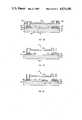
- FIG. 1is a simplified cross-section of a two-terminal cantilever beam shunt element exhibiting hysteresis
- FIG. 2is a schematic diagram of the two-terminal micromechanical shunt device of FIG. 1, showing the inherent interelectrode capacitance between the cantilever beam and the force plate,
- FIG. 3is a simplified cross-section of a three-terminal cantilever beam shunt element exhibiting hysteresis
- FIG. 4is a schematic diagram of the micromechanical shunt device of FIG. 3,
- FIG. 5is a diagrammatic view of another three-terminal cantilever beam shunt element embodiment exhibiting hysteresis
- FIG. 6is a schematic diagram of a basic oscillator employing the hysteretic micromechanical shunt
- FIG. 7is a schematic symbol representing the basic cantilever beam shunt element
- FIG. 8is a schematic diagram showing a plurality of basic hysteretic shunt oscillators packaged as an encoder for use on a communications bus
- FIG. 9is a chart showing the distribution of oscillator energy at discrete frequencies, according to the apparatus of FIG. 8,
- FIG. 10is a plan view of an enlarged portion of the basic hysteretic shunt oscillator when packaged as an encoder
- FIG. 11is a schematic diagram showing a plurality of basic hysteretic shunt elements packaged as a voltage/current encoder for use on a communications bus,
- FIG. 12is a chart showing the second derivative of the electrical current over time resulting from a ramped d-c voltage applied to the communications bus
- FIG. 13is a plan view showing two fused micromechanical shunt elements on a single substrate used as a current shunt encoder for use with a communications bus,
- FIG. 14shows a simplified cross-section of the basic micromechanical shunt device after certain initial fabrication steps
- FIG. 15shows the device of FIG. 14 with a resistance layer covering one terminal
- FIG. 16shows the device of FIG. 15 after certain additional fabrication steps
- FIG. 17shows the device of FIG. 16 prepared for plating of the cantilever beam
- FIG. 18shows the device including a plated centilever beam
- FIG. 19shows a completed two-terminal shunt in cross section
- FIG. 20shows a completed three-terminal shunt in cross section
- FIG. 21shows a plan view of a plurality of cantilever beam elements grouped around a unitary force plate element.
- micromechanical shunt of the present inventionDue to the wide range of microfabrication techniques and the many uses to which the micromechanical shunt of the present invention may be put, several specific embodiments of the invention and examples of how they are made are included herein.
- FIG. 1illustrates pictorially the essential elements of the two-terminal version of the micromechanical shunt 11, while FIG. 2 illustrates the same micromechanical shunt 11 in electrical schematic form.
- An input terminal 100is affixed to a substrate 106, and a cantilever beam 105 having a fixed end and a free end is physically and electrically joined to the terminal 100 at its fixed end. Lying under the free end of the cantilever beam 105 is a contact plate 102, which serves as a force plate and also as the output terminal in this example.
- a d-c voltageis placed across points 100, 102, and cantilever 105 is electrostatically attracted to the contact plate 102. As cantilever 105 comes closer to plate 102, less voltage is required to move the cantilever into closer proximity with plate 102.
- resistance 101is interposed between cantilever beam 105 and contact plate 102.
- a lower charge valueis required to maintain the cantilever 105 in close proximity to contact plate 102 than the charge value required to move the cantilever from its rest position into proximity with contact plate 102, thus the shunt 11 exhibits hysteresis.
- the resistance 101is shown physically located between elements 102, 105, and in FIG. 2, it is shown electrically between cantilever beam 105 and the input terminal 100 for clarity, since it is electrically in series with the input 100, cantilever beam 105, and output 103.
- An interelectrode capacitanceexists between cantilever beam 105 and contact plate 102; it is pictured in FIG.
- FIG. 3illustrates in pictorial form a three-terminal micromechanical shunt according to the present invention
- FIG. 4illustrates schematically the same device connected in a two-terminal configuration.
- contact plate 102, cantilever beam 105, and a field plate 107are separately joined to an insulating substrate 106.
- an input terminal 100is shown connected to the cantilever arm 105
- a resistance 101is connected between cantilever plate 102 and output terminal 103
- the field plate 107which underlies the cantilever beam 105, is also connected to output terminal 103.
- An interelectrode capacitanceexists between field plate 107 and the cantilever arm 105, but is not shown.
- a resistance layermay be deposited between contact plate 102 and cantilever beam 105, as in FIG. 1, in order to avoid short-circuiting the voltage charge applied between the field plate 107 and contact plate 102, or a separate discrete resistor may be electrically inserted between contact plate 102 and terminal 103.
- FIG. 5An alternate embodiment three-terminal shunt 12 is disclosed in FIG. 5, in which a substrate 106 underlies a field plate 107, on which is deposited a resistance layer 101, and on which is in turn mounted a contact plate 102.
- Cantilever beam 105having a free end and a fixed end, is attached at its fixed end to the substrate with its free end suprajacent contact plate 102.
- a field terminal 108extends from the field plate joined to the substrate 106, and an input terminal 100 extends from the fixed end of cantilever beam 105, also joined to the substrate 106.
- Another terminal, output terminal 103is joined to the substrate and to the contact plate 102, generally following the profile of the resistance layer 101 but electrically insulated therefrom.
- micromechanical shunt 10is shown in a relaxation oscillator circuit 13. Applying a voltage between terminals 112 and 113 to resistor 110 and capacitor 111, which form an RC time constant charging circuit, the capacitor charges with time and the voltage level at voltage divider point A increases relative to terminal 113. The voltage across the micromechanical shunt 10, in parallel with capacitor 111, increases similarly. As the voltage increases, the electrostatic charge between contact plate 102 and cantilever beam 105 brings the two together by electrostatic attraction. When the cantilever beam 105 makes contact, capacitor 111 is discharged through resistance 101. The resistance 101 may be either a discrete resistor or a deposited film electrical resistance between the contact plate 102 and the cantilever beam 105.
- FIG. 7represents schematically the micromechanical shunt 10 which includes elements 101, 102, and 105 contained within the dotted line of FIG. 6.
- a plurality of these oscillators 121, 122, 123, 124, 125, 126may be produced together as shown in FIG. 8 and connected in parallel, each being adjusted to a separate frequency.
- Including a fusible link 103, 131, 132, 133, 134, 135 in series with each respective oscillator sectionpermits arranging a plurality of such oscillators into an oscillator signature system. Except for the addition of its respective fusible link, each oscillator is substantially identical to the oscillator 13 shown in FIG. 6.
- Interrupting the power supply line to the oscillator by opening one or more fusible links in a predetermined patternresults in an identifiable encoding pattern.
- Including a plurality of such fusible link oscillators at a single location or at a single telemetry locationas is facilitated by fabricating several such oscillators on a single chip, enables discrete encoding of the location, function, or station in the telemetry system, which encoding pattern may be remotely sensed or detected. This is especially useful for identifying stations in a high-speed, serial bus telemetry communications configuration.
- FIG. 9there is shown an amplitude versus frequency graph of a station such as that in FIG. 8 in which the fusible links 133, 135 of oscillators 124, 126 are opened and an interrogation voltage applied to communication bus 127, 128 (identified as terminals 1 and 2, respectively). Returned along the bus are frequencies F1, F2, F3, and F5; with F4 and F6 being absent.
- the presence or absence of energy at each particular frequencyis sensed in accordance with conventional spectrum analysis techniques. If the presence of a measurable amplitude of energy at a particular frequency is coded as a binary 1, the station represented in FIG. 9 is coded 111010, and is specifically identifiable from among a plurality of similarly coded stations.
- FIG. 10there is shown a simplified plan view of an individual oscillator section 121 such as forms the basis of an oscillator signature system 14 on a single substrate 106 (remaining oscillator sections, which are identical, are not shown).
- the micromechanical shunt 10is connected from ground bus 128 in parallel with capacitor 111 which is in series with both resistor 110 and fusible link 130 to supply bus 127.
- a pad 120joins resistance 110 and fusible link 130 and in combination with bus 127 provides a contact area for opening fusible link 130 by passing a high current therethrough. In this manner, the identification encoding can be performed to reflect the coding for a given station or point.
- a resistance layer(not visible in this view) is ordinarily included underlying the free end of cantilever beam 105 to limit contact current through the cantilever beam to reasonable values.
- Point Ais the voltage divider point described in the discussion associated with FIG. 6.
- FIG. 11there is shown a series of parallel-connected micromechanical hysteretic shunts 10 similar to those of FIG. 7, each connected with its own respective fusible link 130, 131, 132, 133, 134, 135, 136, 137, and forming an electrical current signature encoding system 15.
- Each successive micromechanical shunt circuit element 140, 141, 142, 143, 144, 145, 146, 147has a slightly higher closure threshold voltage, determined mainly by the dimensions of the cantilever beam contained therein.
- the shunt closure threshold voltagesare selected above the normal operating range of the equipment at the post, station, or operating site.
- Interrogationis performed by applying a ramped d-c voltage (which includes all of the threshold voltages being interrogated) to communications bus (127, 128 and monitoring the second derivative of the current in the line. In this manner, a series of spikes representative of the coded pattern, is obtained. See FIG. 12, in which bits B1-B8 represent shunt elements 140-147, inclusive. If fusible links 132 and 135 are open, and binary coding is used, FIG. 12 represents a 11011011 8-bit encoding.
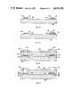
- FIG. 13A simplified successful layout pattern for the circuit of FIG. 11 is shown in FIG. 13, in which a fused micromechanical shunt 140 having a cantilever beam 105 connected in series with a fusible link 130 is mounted on a substrate 106 between two terminals 127, 128.
- the cantilever beams 105, 109are connected with the respective fusible links 130, 131 via fuse pads 120, 119 and are progressively shorter.
- This variation in lengthprovides one of several ways to vary the threshold voltage of the shunt because longer cantilever beams require lower threshold voltages for closure, all other characteristics being equal.
- the resistance of the individual shunt elements 10must be selected such that the increment of current produced at shunt activation is detectable above the noise in the current flowing through the host station or site. Consideration must also be given to the threshold voltage separations between each shunt element as limited by the maximum permissible voltage values. Manufacturing capabilities are likely limitations in the differences in threshold voltages between shunts. Vibration immunity is a further consideration.
- the frequencycan be calculated by considering the amount of time it takes to raise V 1 (or to charge the capacitor) from V off (the voltage at which the switch opens) to V on (the voltage at which the switch closes) and the time it takes to decrease V 1 (discharge the capacitor) from V on to V off .
- the sum of these timesis the period of oscillation.
- the period of oscillationis:
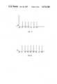
- FIG. 21shows a plurality of cantilever beam elements 105 fabricated around a single force plate 102. Each cantilever beam is of a different length.
- the metallizationsare on substrate 106, and include contact terminal 103, electrically connected to force plate 102, a bus 128 connecting the various elements; contact pads 100; fusible links 130 connected between bus 128 and contact pads 100; and the cantilever beams 105.
- micromechanical electric shunt devicesThe following is a generalized process for making micromechanical electric shunt devices according to the various embodiments included in this disclosure.
- a glass substrate 106is prepared by washing in detergent solution in an ultrasonic cleaner, rinsed thoroughly in deionized water, then blow-dried with dry nitrogen.
- a layer of chromium 151, from 10 to 1,000 Angstroms thickis deposited on the glass substrate 106, followed by deposition of a 2,000 to 3,000 Angstrom gold layer.
- a photolithographic resist layeris applied and prebaked, then exposed to a suitable mask and developed to produce a first, input terminal area 100 and a second terminal surface area 102 which serves as an output terminal area in two-terminal devices 11 and in three-terminal devices 12.
- a third surface areais formed in an identical manner for a force plate generally lying between first terminal surface area 100 and second terminal surface area 102.
- the undesired materialis etched way in conventional manner to leave the terminal areas. Plasma/sputter etching produces a clean, angled profile and is preferred to wet etching.
- a resistance layer 101may be desired at terminal 102, especially in two-terminal devices.
- Suitable resistive materialsuch as germanium, a copper oxide, or doped silicon, preferably silicon doped with aluminum, is deposited on terminal 102.
- aluminum-bearing siliconis deposited and the surplus removed by standard photolithographic patterning and etching techniques, preferably by dry etching in order to provide a suitable profile, resulting in resistance layer 101 covering terminal 102.
- FIG. 16there is shown a substrate 106 including thereon terminals 100, 102 and resistance layer 101 according to the preceding procedure.
- a substantial nickel layer 152is deposited over the surface of the wafer by sputtering, which layer 152 generally follows the profile of the built-up areas at 100 and 101/102.
- a nickel layer having a thickness of 1 to 2 micronsis desired.
- a photoresist layer 153is patterned according to conventional photolithographic methods with etch holes at 154 and 155 precisely aligned over terminals 100 and 102. Holes 154, 155 may be separately etched using separate photolithographic masks and etching steps.
- a lineis used to show the boundary between the nickel layer 152 and photoresist layer 153 before and after the portion of the step where the holes 154, 155 are etched.
- a cantilever mount hole 154 and a cantilever contact hole 155are carefully etched; the contact hole 155 is etched to a depth of approximately 3,000 to 10,000 Angstroms and the mount hole 154 is etched to a depth of 1 to 2 microns or until the surface of gold layer 150 of terminal 100 is exposed, so as to provide a plating contact surface for subsequent forming of the cantilever beam.
- etch resist layer 153completely covers the nickel layer 152, except for holes 154 and 155.
- FIG. 17the hole etch resist pattern has been removed and the desired cantilever plating pattern substituted, using standard photolithographic techniques. Since FIG. 17 is a vertical cross-section along the longitudinal axis of the desired cantilever beam 105 shape, the plating resist layers 156 of the extreme left and right of the figure are shown as cross-sections, while an exposed resist face (boundary for the cantilever beam edge) is shown at the center where the cantilever beam 105 will be formed.
- FIG. 18shows the deposition of a gold layer onto the nickel layer by plating to a thickness of between 1 and 10 microns in a cantilever beam plating resist channel provided in a beam-defining area to form cantilever 105.
- the beam 105may be formed between 5 microns and 1,000 microns wide, preferably between 50 microns and 200 microns wide; between 1 and 10 microns thick, preferably between 2 and 6 microns thick; and of a length between 1 and 200 mils, preferably between 4 and 120 mils, and most preferably between 4 and 30 mils.
- the exposed nickelis cleaned with a 5 to 10 percent solution of hydrochloric acid and then the beam 105 is formed by plating the exposed nickel surface to the desired thickness with an acid gold solution.
- the plating resist 156is removed (FIG. 19) and then the entire nickel layer 152 is removed by etching in a strong solution of nitric acid, thereby relieving cantilever beam 105.
- suitable nickel etchantsinclude combinations of nitric, acetic and sulfuric acids or ferric chloride.
- the deviceis cleaned by placing it in alcohol to lower the surface tension, then immersed in water, and dried; a slightly elevated temperature facilitates drying. Drying of shorter beam lengths may be improved by spinning until dry at relatively low speeds, such as less than 500 rpm.
- FIG. 20reveals a three-terminal micromechanical shunt 12 formed according to the same process, save for addition of an additional pad surface area 107 as a force plate, and omitting resistance 101 and the process steps associated therewith.
Landscapes
- Engineering & Computer Science (AREA)
- Physics & Mathematics (AREA)
- Manufacturing & Machinery (AREA)
- General Physics & Mathematics (AREA)
- Theoretical Computer Science (AREA)
- Microelectronics & Electronic Packaging (AREA)
- Electromagnetism (AREA)
- Micromachines (AREA)
Abstract
Description
T=t.sub.1 +t.sub.2,
αV.sub.O <V.sub.off <V.sub.on
Claims (13)
Priority Applications (2)
| Application Number | Priority Date | Filing Date | Title |
|---|---|---|---|
| US06/606,065US4674180A (en) | 1984-05-01 | 1984-05-01 | Method of making a micromechanical electric shunt |
| US07/012,092US4959515A (en) | 1984-05-01 | 1987-02-06 | Micromechanical electric shunt and encoding devices made therefrom |
Applications Claiming Priority (1)
| Application Number | Priority Date | Filing Date | Title |
|---|---|---|---|
| US06/606,065US4674180A (en) | 1984-05-01 | 1984-05-01 | Method of making a micromechanical electric shunt |
Related Child Applications (1)
| Application Number | Title | Priority Date | Filing Date |
|---|---|---|---|
| US07/012,092DivisionUS4959515A (en) | 1984-05-01 | 1987-02-06 | Micromechanical electric shunt and encoding devices made therefrom |
Publications (1)
| Publication Number | Publication Date |
|---|---|
| US4674180Atrue US4674180A (en) | 1987-06-23 |
Family
ID=24426384
Family Applications (1)
| Application Number | Title | Priority Date | Filing Date |
|---|---|---|---|
| US06/606,065Expired - LifetimeUS4674180A (en) | 1984-05-01 | 1984-05-01 | Method of making a micromechanical electric shunt |
Country Status (1)
| Country | Link |
|---|---|
| US (1) | US4674180A (en) |
Cited By (74)
| Publication number | Priority date | Publication date | Assignee | Title |
|---|---|---|---|---|
| US4849070A (en)* | 1988-09-14 | 1989-07-18 | The United States Of America As Represented By The Secretary Of The Army | Process for fabricating three-dimensional, free-standing microstructures |
| US4959515A (en)* | 1984-05-01 | 1990-09-25 | The Foxboro Company | Micromechanical electric shunt and encoding devices made therefrom |
| US5016072A (en)* | 1988-01-13 | 1991-05-14 | The Charles Stark Draper Laboratory, Inc. | Semiconductor chip gyroscopic transducer |
| US5126812A (en)* | 1990-02-14 | 1992-06-30 | The Charles Stark Draper Laboratory, Inc. | Monolithic micromechanical accelerometer |
| US5129983A (en)* | 1991-02-25 | 1992-07-14 | The Charles Stark Draper Laboratory, Inc. | Method of fabrication of large area micromechanical devices |
| JPH04306520A (en)* | 1990-11-01 | 1992-10-29 | Hughes Aircraft Co | Micromachining switch and manufacture thereof |
| US5165289A (en)* | 1990-07-10 | 1992-11-24 | Johnson Service Company | Resonant mechanical sensor |
| WO1992015109A3 (en)* | 1991-02-15 | 1993-01-07 | Guenther Niessen | Arrangement of control switching and control device therefor |
| US5203208A (en)* | 1991-04-29 | 1993-04-20 | The Charles Stark Draper Laboratory | Symmetrical micromechanical gyroscope |
| US5216490A (en)* | 1988-01-13 | 1993-06-01 | Charles Stark Draper Laboratory, Inc. | Bridge electrodes for microelectromechanical devices |
| US5238435A (en)* | 1987-06-10 | 1993-08-24 | U.S. Philips Corporation | Liquid crystal display device and method of manufacturing such a display device |
| US5258591A (en)* | 1991-10-18 | 1993-11-02 | Westinghouse Electric Corp. | Low inductance cantilever switch |
| US5262000A (en)* | 1989-09-26 | 1993-11-16 | British Telecommunications Public Limited Company | Method for making micromechanical switch |
| US5331852A (en)* | 1991-09-11 | 1994-07-26 | The Charles Stark Draper Laboratory, Inc. | Electromagnetic rebalanced micromechanical transducer |
| US5349855A (en)* | 1992-04-07 | 1994-09-27 | The Charles Stark Draper Laboratory, Inc. | Comb drive micromechanical tuning fork gyro |
| US5374792A (en)* | 1993-01-04 | 1994-12-20 | General Electric Company | Micromechanical moving structures including multiple contact switching system |
| US5408877A (en)* | 1992-03-16 | 1995-04-25 | The Charles Stark Draper Laboratory, Inc. | Micromechanical gyroscopic transducer with improved drive and sense capabilities |
| US5410799A (en)* | 1993-03-17 | 1995-05-02 | National Semiconductor Corporation | Method of making electrostatic switches for integrated circuits |
| US5439552A (en)* | 1992-11-04 | 1995-08-08 | Csem - Centre Suisse D'electronique Et De Microtechnique Sa | Process of fabricating an enlongated microstructure element on a substrate |
| US5472539A (en)* | 1994-06-06 | 1995-12-05 | General Electric Company | Methods for forming and positioning moldable permanent magnets on electromagnetically actuated microfabricated components |
| US5475353A (en)* | 1994-09-30 | 1995-12-12 | General Electric Company | Micromachined electromagnetic switch with fixed on and off positions using three magnets |
| US5479042A (en)* | 1993-02-01 | 1995-12-26 | Brooktree Corporation | Micromachined relay and method of forming the relay |
| US5507911A (en)* | 1990-10-17 | 1996-04-16 | The Charles Stark Draper Laboratory, Inc. | Monolithic micromechanical vibrating string accelerometer with trimmable resonant frequency |
| US5581035A (en)* | 1994-08-29 | 1996-12-03 | The Charles Stark Draper Laboratory, Inc. | Micromechanical sensor with a guard band electrode |
| US5605598A (en)* | 1990-10-17 | 1997-02-25 | The Charles Stark Draper Laboratory Inc. | Monolithic micromechanical vibrating beam accelerometer with trimmable resonant frequency |
| US5619061A (en)* | 1993-07-27 | 1997-04-08 | Texas Instruments Incorporated | Micromechanical microwave switching |
| US5635739A (en)* | 1990-02-14 | 1997-06-03 | The Charles Stark Draper Laboratory, Inc. | Micromechanical angular accelerometer with auxiliary linear accelerometer |
| US5635639A (en)* | 1991-09-11 | 1997-06-03 | The Charles Stark Draper Laboratory, Inc. | Micromechanical tuning fork angular rate sensor |
| US5638946A (en)* | 1996-01-11 | 1997-06-17 | Northeastern University | Micromechanical switch with insulated switch contact |
| US5646348A (en)* | 1994-08-29 | 1997-07-08 | The Charles Stark Draper Laboratory, Inc. | Micromechanical sensor with a guard band electrode and fabrication technique therefor |
| US5650568A (en)* | 1993-02-10 | 1997-07-22 | The Charles Stark Draper Laboratory, Inc. | Gimballed vibrating wheel gyroscope having strain relief features |
| US5658636A (en)* | 1995-01-27 | 1997-08-19 | Carnegie Mellon University | Method to prevent adhesion of micromechanical structures |
| US5725729A (en)* | 1994-09-26 | 1998-03-10 | The Charles Stark Draper Laboratory, Inc. | Process for micromechanical fabrication |
| US5767405A (en)* | 1992-04-07 | 1998-06-16 | The Charles Stark Draper Laboratory, Inc. | Comb-drive micromechanical tuning fork gyroscope with piezoelectric readout |
| US5783973A (en)* | 1997-02-24 | 1998-07-21 | The Charles Stark Draper Laboratory, Inc. | Temperature insensitive silicon oscillator and precision voltage reference formed therefrom |
| EP0845728A3 (en)* | 1996-11-27 | 1998-07-22 | Xerox Corporation | Printed dielectric substrate for microelectromechanical systems |
| US5817942A (en)* | 1996-02-28 | 1998-10-06 | The Charles Stark Draper Laboratory, Inc. | Capacitive in-plane accelerometer |
| US5892153A (en)* | 1996-11-21 | 1999-04-06 | The Charles Stark Draper Laboratory, Inc. | Guard bands which control out-of-plane sensitivities in tuning fork gyroscopes and other sensors |
| US5911156A (en)* | 1997-02-24 | 1999-06-08 | The Charles Stark Draper Laboratory, Inc. | Split electrode to minimize charge transients, motor amplitude mismatch errors, and sensitivity to vertical translation in tuning fork gyros and other devices |
| US5943223A (en)* | 1997-10-15 | 1999-08-24 | Reliance Electric Industrial Company | Electric switches for reducing on-state power loss |
| US5952574A (en)* | 1997-04-29 | 1999-09-14 | The Charles Stark Draper Laboratory, Inc. | Trenches to reduce charging effects and to control out-of-plane sensitivities in tuning fork gyroscopes and other sensors |
| WO1999063562A1 (en)* | 1998-06-04 | 1999-12-09 | Wang-Electro-Opto Corporation | Low-voltage, electrostatic type microelectromechanical system switches for radio-frequency applications |
| US6058027A (en)* | 1999-02-16 | 2000-05-02 | Maxim Integrated Products, Inc. | Micromachined circuit elements driven by micromachined DC-to-DC converter on a common substrate |
| US6246243B1 (en)* | 2000-01-21 | 2001-06-12 | Analog Devices, Inc. | Semi-fusible link system |
| US6323834B1 (en) | 1998-10-08 | 2001-11-27 | International Business Machines Corporation | Micromechanical displays and fabrication method |
| US6373007B1 (en) | 2000-04-19 | 2002-04-16 | The United States Of America As Represented By The Secretary Of The Air Force | Series and shunt mems RF switch |
| WO2002068046A1 (en) | 2000-11-03 | 2002-09-06 | Medtronic, Inc. | Mems switching circuit and method for an implantable medical device |
| US6570750B1 (en) | 2000-04-19 | 2003-05-27 | The United States Of America As Represented By The Secretary Of The Air Force | Shunted multiple throw MEMS RF switch |
| US20030149363A1 (en)* | 1998-11-19 | 2003-08-07 | Acuson Corporation | Diagnostic medical ultrasound systems and transducers utilizing micro-mechanical components |
| US6678943B1 (en)* | 1999-06-04 | 2004-01-20 | The Board Of Trustees Of The University Of Illinois | Method of manufacturing a microelectromechanical switch |
| US20040035206A1 (en)* | 2002-03-26 | 2004-02-26 | Ward Paul A. | Microelectromechanical sensors having reduced signal bias errors and methods of manufacturing the same |
| JP2004117368A (en)* | 2003-10-14 | 2004-04-15 | Tokyo Electron Ltd | Acoustic sensor |
| US20040198081A1 (en)* | 1993-11-16 | 2004-10-07 | Eldridge Benjamin N. | Microelectronic spring contact elements |
| WO2004054088A3 (en)* | 2002-12-10 | 2004-12-02 | Koninkl Philips Electronics Nv | Driving of an array of micro-electro-mechanical-system (mems) elements |
| US20040244191A1 (en)* | 2001-10-25 | 2004-12-09 | Bruce Orr | Method of fabrication of micro-devices |
| US20060269186A1 (en)* | 2005-05-17 | 2006-11-30 | James Frame | High-impedance attenuator |
| US20070040637A1 (en)* | 2005-08-19 | 2007-02-22 | Yee Ian Y K | Microelectromechanical switches having mechanically active components which are electrically isolated from components of the switch used for the transmission of signals |
| US20070115082A1 (en)* | 2005-10-03 | 2007-05-24 | Analog Devices, Inc. | MEMS Switch Contact System |
| US20070223267A1 (en)* | 2004-06-15 | 2007-09-27 | Robert Kazinczi | Arrangement and Method for Controlling a Micromechanical Element |
| US20080151464A1 (en)* | 2006-12-22 | 2008-06-26 | Analog Devices, Inc. | Method and Apparatus for Driving a Switch |
| US20080157237A1 (en)* | 2006-12-29 | 2008-07-03 | Myung-Soo Kim | Switching device and method of fabricating the same |
| US7601039B2 (en) | 1993-11-16 | 2009-10-13 | Formfactor, Inc. | Microelectronic contact structure and method of making same |
| US20100005884A1 (en)* | 2008-07-09 | 2010-01-14 | Weinberg Marc S | High Performance Sensors and Methods for Forming the Same |
| US20100012471A1 (en)* | 2002-10-25 | 2010-01-21 | Analog Devices, Inc. | Micro-Machined Relay |
| US20100068854A1 (en)* | 2005-10-03 | 2010-03-18 | Analog Devices, Inc. | MEMS Switch Capping and Passivation Method |
| US20100237738A1 (en)* | 2009-03-17 | 2010-09-23 | Charles Gordon Smith | Moving a free-standing structure between high and low adhesion states |
| US8033838B2 (en) | 1996-02-21 | 2011-10-11 | Formfactor, Inc. | Microelectronic contact structure |
| EP2479887A1 (en)* | 2011-01-19 | 2012-07-25 | Alcatel Lucent | Electro-mechanical radio frequency signal generator and method of operating an electro-mechanical radio frequency signal generator |
| US8373428B2 (en) | 1993-11-16 | 2013-02-12 | Formfactor, Inc. | Probe card assembly and kit, and methods of making same |
| JP2013232391A (en)* | 2011-07-29 | 2013-11-14 | General Electric Co <Ge> | Electrical distribution system |
| US20150334851A1 (en)* | 2008-01-17 | 2015-11-19 | Harris Corporation | Three-dimensional liquid crystal polymer multilayer circuit board including membrane switch and related methods |
| JP2015213994A (en)* | 2014-05-12 | 2015-12-03 | 国立大学法人東北大学 | Digital circuit utilizing nano-mechanical switch |
| US20170268698A1 (en)* | 2016-03-15 | 2017-09-21 | Dunan Microstaq, Inc. | Mems based solenoid valve |
| US20240203669A1 (en)* | 2022-12-06 | 2024-06-20 | The Regents Of The University Of California | Bit rate-adapting resoswitch |
Citations (6)
| Publication number | Priority date | Publication date | Assignee | Title |
|---|---|---|---|---|
| US3321602A (en)* | 1965-07-12 | 1967-05-23 | Sprague Electric Co | Voltage-sensitive multiple switch |
| US3413573A (en)* | 1965-06-18 | 1968-11-26 | Westinghouse Electric Corp | Microelectronic frequency selective apparatus with vibratory member and means responsive thereto |
| US3509470A (en)* | 1968-03-27 | 1970-04-28 | Sylvania Electric Prod | Electrostatic protection device |
| US3681134A (en)* | 1968-05-31 | 1972-08-01 | Westinghouse Electric Corp | Microelectronic conductor configurations and methods of making the same |
| US3686593A (en)* | 1969-03-07 | 1972-08-22 | Int Standard Electric Corp | Electromechanical resonator |
| US4289846A (en)* | 1979-12-28 | 1981-09-15 | General Electric Company | Process for forming low-reactance interconnections on semiconductors |
- 1984
- 1984-05-01USUS06/606,065patent/US4674180A/ennot_activeExpired - Lifetime
Patent Citations (6)
| Publication number | Priority date | Publication date | Assignee | Title |
|---|---|---|---|---|
| US3413573A (en)* | 1965-06-18 | 1968-11-26 | Westinghouse Electric Corp | Microelectronic frequency selective apparatus with vibratory member and means responsive thereto |
| US3321602A (en)* | 1965-07-12 | 1967-05-23 | Sprague Electric Co | Voltage-sensitive multiple switch |
| US3509470A (en)* | 1968-03-27 | 1970-04-28 | Sylvania Electric Prod | Electrostatic protection device |
| US3681134A (en)* | 1968-05-31 | 1972-08-01 | Westinghouse Electric Corp | Microelectronic conductor configurations and methods of making the same |
| US3686593A (en)* | 1969-03-07 | 1972-08-22 | Int Standard Electric Corp | Electromechanical resonator |
| US4289846A (en)* | 1979-12-28 | 1981-09-15 | General Electric Company | Process for forming low-reactance interconnections on semiconductors |
Non-Patent Citations (2)
| Title |
|---|
| Holland, L. & Petersen, K. E., "Bottom Contacting Micromechanical Switching Geometry", IBM Tech. Disclosure Bull., vol. 21, No. 3, Aug. '78, pp. 1207-1208. |
| Holland, L. & Petersen, K. E., Bottom Contacting Micromechanical Switching Geometry , IBM Tech. Disclosure Bull., vol. 21, No. 3, Aug. 78, pp. 1207 1208.* |
Cited By (108)
| Publication number | Priority date | Publication date | Assignee | Title |
|---|---|---|---|---|
| US4959515A (en)* | 1984-05-01 | 1990-09-25 | The Foxboro Company | Micromechanical electric shunt and encoding devices made therefrom |
| US5238435A (en)* | 1987-06-10 | 1993-08-24 | U.S. Philips Corporation | Liquid crystal display device and method of manufacturing such a display device |
| US5016072A (en)* | 1988-01-13 | 1991-05-14 | The Charles Stark Draper Laboratory, Inc. | Semiconductor chip gyroscopic transducer |
| US5216490A (en)* | 1988-01-13 | 1993-06-01 | Charles Stark Draper Laboratory, Inc. | Bridge electrodes for microelectromechanical devices |
| US4849070A (en)* | 1988-09-14 | 1989-07-18 | The United States Of America As Represented By The Secretary Of The Army | Process for fabricating three-dimensional, free-standing microstructures |
| US5262000A (en)* | 1989-09-26 | 1993-11-16 | British Telecommunications Public Limited Company | Method for making micromechanical switch |
| US5635739A (en)* | 1990-02-14 | 1997-06-03 | The Charles Stark Draper Laboratory, Inc. | Micromechanical angular accelerometer with auxiliary linear accelerometer |
| US5126812A (en)* | 1990-02-14 | 1992-06-30 | The Charles Stark Draper Laboratory, Inc. | Monolithic micromechanical accelerometer |
| US5165289A (en)* | 1990-07-10 | 1992-11-24 | Johnson Service Company | Resonant mechanical sensor |
| US5605598A (en)* | 1990-10-17 | 1997-02-25 | The Charles Stark Draper Laboratory Inc. | Monolithic micromechanical vibrating beam accelerometer with trimmable resonant frequency |
| US5760305A (en)* | 1990-10-17 | 1998-06-02 | The Charles Stark Draper Laboratory, Inc. | Monolithic micromechanical vibrating beam accelerometer with trimmable resonant frequency |
| US5507911A (en)* | 1990-10-17 | 1996-04-16 | The Charles Stark Draper Laboratory, Inc. | Monolithic micromechanical vibrating string accelerometer with trimmable resonant frequency |
| US5969250A (en)* | 1990-10-17 | 1999-10-19 | The Charles Stark Draper Laboratory, Inc. | Micromechanical accelerometer having a peripherally suspended proof mass |
| JP2693065B2 (en) | 1990-11-01 | 1997-12-17 | エイチイー・ホールディングス・インコーポレーテッド・ディービーエー・ヒューズ・エレクトロニクス | Micromachined switch and manufacturing method thereof |
| EP0484142A3 (en)* | 1990-11-01 | 1993-03-31 | Hughes Aircraft Company | Micro-machined switch and method of fabrication |
| JPH04306520A (en)* | 1990-11-01 | 1992-10-29 | Hughes Aircraft Co | Micromachining switch and manufacture thereof |
| WO1992015109A3 (en)* | 1991-02-15 | 1993-01-07 | Guenther Niessen | Arrangement of control switching and control device therefor |
| US5129983A (en)* | 1991-02-25 | 1992-07-14 | The Charles Stark Draper Laboratory, Inc. | Method of fabrication of large area micromechanical devices |
| US5203208A (en)* | 1991-04-29 | 1993-04-20 | The Charles Stark Draper Laboratory | Symmetrical micromechanical gyroscope |
| US5505084A (en)* | 1991-09-11 | 1996-04-09 | The Charles Stark Draper Laboratory, Inc. | Micromechanical tuning fork angular rate sensor |
| US5635639A (en)* | 1991-09-11 | 1997-06-03 | The Charles Stark Draper Laboratory, Inc. | Micromechanical tuning fork angular rate sensor |
| US5331852A (en)* | 1991-09-11 | 1994-07-26 | The Charles Stark Draper Laboratory, Inc. | Electromagnetic rebalanced micromechanical transducer |
| US5258591A (en)* | 1991-10-18 | 1993-11-02 | Westinghouse Electric Corp. | Low inductance cantilever switch |
| US5408877A (en)* | 1992-03-16 | 1995-04-25 | The Charles Stark Draper Laboratory, Inc. | Micromechanical gyroscopic transducer with improved drive and sense capabilities |
| US5515724A (en)* | 1992-03-16 | 1996-05-14 | The Charles Stark Draper Laboratory, Inc. | Micromechanical gyroscopic transducer with improved drive and sense capabilities |
| US5496436A (en)* | 1992-04-07 | 1996-03-05 | The Charles Stark Draper Laboratory, Inc. | Comb drive micromechanical tuning fork gyro fabrication method |
| US5767405A (en)* | 1992-04-07 | 1998-06-16 | The Charles Stark Draper Laboratory, Inc. | Comb-drive micromechanical tuning fork gyroscope with piezoelectric readout |
| US5349855A (en)* | 1992-04-07 | 1994-09-27 | The Charles Stark Draper Laboratory, Inc. | Comb drive micromechanical tuning fork gyro |
| US5439552A (en)* | 1992-11-04 | 1995-08-08 | Csem - Centre Suisse D'electronique Et De Microtechnique Sa | Process of fabricating an enlongated microstructure element on a substrate |
| US5374792A (en)* | 1993-01-04 | 1994-12-20 | General Electric Company | Micromechanical moving structures including multiple contact switching system |
| US5479042A (en)* | 1993-02-01 | 1995-12-26 | Brooktree Corporation | Micromachined relay and method of forming the relay |
| US5650568A (en)* | 1993-02-10 | 1997-07-22 | The Charles Stark Draper Laboratory, Inc. | Gimballed vibrating wheel gyroscope having strain relief features |
| US5410799A (en)* | 1993-03-17 | 1995-05-02 | National Semiconductor Corporation | Method of making electrostatic switches for integrated circuits |
| US5619061A (en)* | 1993-07-27 | 1997-04-08 | Texas Instruments Incorporated | Micromechanical microwave switching |
| US8373428B2 (en) | 1993-11-16 | 2013-02-12 | Formfactor, Inc. | Probe card assembly and kit, and methods of making same |
| US7601039B2 (en) | 1993-11-16 | 2009-10-13 | Formfactor, Inc. | Microelectronic contact structure and method of making same |
| US20040198081A1 (en)* | 1993-11-16 | 2004-10-07 | Eldridge Benjamin N. | Microelectronic spring contact elements |
| US7579269B2 (en) | 1993-11-16 | 2009-08-25 | Formfactor, Inc. | Microelectronic spring contact elements |
| US5472539A (en)* | 1994-06-06 | 1995-12-05 | General Electric Company | Methods for forming and positioning moldable permanent magnets on electromagnetically actuated microfabricated components |
| US5646348A (en)* | 1994-08-29 | 1997-07-08 | The Charles Stark Draper Laboratory, Inc. | Micromechanical sensor with a guard band electrode and fabrication technique therefor |
| US5581035A (en)* | 1994-08-29 | 1996-12-03 | The Charles Stark Draper Laboratory, Inc. | Micromechanical sensor with a guard band electrode |
| US5725729A (en)* | 1994-09-26 | 1998-03-10 | The Charles Stark Draper Laboratory, Inc. | Process for micromechanical fabrication |
| US5475353A (en)* | 1994-09-30 | 1995-12-12 | General Electric Company | Micromachined electromagnetic switch with fixed on and off positions using three magnets |
| US5772902A (en)* | 1995-01-27 | 1998-06-30 | Carnegie Mellon University | Method to prevent adhesion of micromechanical structures |
| US5658636A (en)* | 1995-01-27 | 1997-08-19 | Carnegie Mellon University | Method to prevent adhesion of micromechanical structures |
| US5638946A (en)* | 1996-01-11 | 1997-06-17 | Northeastern University | Micromechanical switch with insulated switch contact |
| US8033838B2 (en) | 1996-02-21 | 2011-10-11 | Formfactor, Inc. | Microelectronic contact structure |
| US5817942A (en)* | 1996-02-28 | 1998-10-06 | The Charles Stark Draper Laboratory, Inc. | Capacitive in-plane accelerometer |
| US5892153A (en)* | 1996-11-21 | 1999-04-06 | The Charles Stark Draper Laboratory, Inc. | Guard bands which control out-of-plane sensitivities in tuning fork gyroscopes and other sensors |
| EP0845728A3 (en)* | 1996-11-27 | 1998-07-22 | Xerox Corporation | Printed dielectric substrate for microelectromechanical systems |
| US5911156A (en)* | 1997-02-24 | 1999-06-08 | The Charles Stark Draper Laboratory, Inc. | Split electrode to minimize charge transients, motor amplitude mismatch errors, and sensitivity to vertical translation in tuning fork gyros and other devices |
| US5783973A (en)* | 1997-02-24 | 1998-07-21 | The Charles Stark Draper Laboratory, Inc. | Temperature insensitive silicon oscillator and precision voltage reference formed therefrom |
| US5952574A (en)* | 1997-04-29 | 1999-09-14 | The Charles Stark Draper Laboratory, Inc. | Trenches to reduce charging effects and to control out-of-plane sensitivities in tuning fork gyroscopes and other sensors |
| US5943223A (en)* | 1997-10-15 | 1999-08-24 | Reliance Electric Industrial Company | Electric switches for reducing on-state power loss |
| WO1999063562A1 (en)* | 1998-06-04 | 1999-12-09 | Wang-Electro-Opto Corporation | Low-voltage, electrostatic type microelectromechanical system switches for radio-frequency applications |
| US6020564A (en)* | 1998-06-04 | 2000-02-01 | Wang Electro-Opto Corporation | Low-voltage long life electrostatic microelectromechanical system switches for radio-frequency applications |
| US6377233B2 (en) | 1998-10-08 | 2002-04-23 | International Business Machines Corporation | Micromechanical display and fabrication method |
| US6323834B1 (en) | 1998-10-08 | 2001-11-27 | International Business Machines Corporation | Micromechanical displays and fabrication method |
| US7549962B2 (en)* | 1998-11-19 | 2009-06-23 | Siemens Medical Solutions Usa, Inc. | Diagnostic medical ultrasound systems and transducers utilizing micro-mechanical components |
| US20030149363A1 (en)* | 1998-11-19 | 2003-08-07 | Acuson Corporation | Diagnostic medical ultrasound systems and transducers utilizing micro-mechanical components |
| US6058027A (en)* | 1999-02-16 | 2000-05-02 | Maxim Integrated Products, Inc. | Micromachined circuit elements driven by micromachined DC-to-DC converter on a common substrate |
| US6678943B1 (en)* | 1999-06-04 | 2004-01-20 | The Board Of Trustees Of The University Of Illinois | Method of manufacturing a microelectromechanical switch |
| US6246243B1 (en)* | 2000-01-21 | 2001-06-12 | Analog Devices, Inc. | Semi-fusible link system |
| US6570750B1 (en) | 2000-04-19 | 2003-05-27 | The United States Of America As Represented By The Secretary Of The Air Force | Shunted multiple throw MEMS RF switch |
| US6373007B1 (en) | 2000-04-19 | 2002-04-16 | The United States Of America As Represented By The Secretary Of The Air Force | Series and shunt mems RF switch |
| WO2002068046A1 (en) | 2000-11-03 | 2002-09-06 | Medtronic, Inc. | Mems switching circuit and method for an implantable medical device |
| US20040244191A1 (en)* | 2001-10-25 | 2004-12-09 | Bruce Orr | Method of fabrication of micro-devices |
| US20040035206A1 (en)* | 2002-03-26 | 2004-02-26 | Ward Paul A. | Microelectromechanical sensors having reduced signal bias errors and methods of manufacturing the same |
| US8279026B2 (en) | 2002-10-25 | 2012-10-02 | Analog Devices, Inc. | Micro-machined relay |
| US20100012471A1 (en)* | 2002-10-25 | 2010-01-21 | Analog Devices, Inc. | Micro-Machined Relay |
| JP2006509643A (en)* | 2002-12-10 | 2006-03-23 | コーニンクレッカ フィリップス エレクトロニクス エヌ ヴィ | Driving an array of MEMS (Micro-Electro-Mechanical-System) elements |
| KR101140689B1 (en)* | 2002-12-10 | 2012-05-03 | 에프코스 아게 | Driving of an array of micro-electro-mechanical-systemmems elements |
| WO2004054088A3 (en)* | 2002-12-10 | 2004-12-02 | Koninkl Philips Electronics Nv | Driving of an array of micro-electro-mechanical-system (mems) elements |
| CN1723606B (en)* | 2002-12-10 | 2011-01-12 | 爱普科斯公司 | MEMS cell array and driving method thereof |
| US20060050350A1 (en)* | 2002-12-10 | 2006-03-09 | Koninklijke Philips Electronics N.V. | Driving of an array of micro-electro-mechanical-system (mems) elements |
| JP2004117368A (en)* | 2003-10-14 | 2004-04-15 | Tokyo Electron Ltd | Acoustic sensor |
| US7613039B2 (en)* | 2004-06-15 | 2009-11-03 | Cavendish Kinetics B.V. | Arrangement and method for controlling a micromechanical element |
| US20070223267A1 (en)* | 2004-06-15 | 2007-09-27 | Robert Kazinczi | Arrangement and Method for Controlling a Micromechanical Element |
| US7965547B2 (en) | 2004-06-15 | 2011-06-21 | Cavendish Kinetics, Inc. | Arrangement and method for controlling a micromechanical element |
| US20100080052A1 (en)* | 2004-06-15 | 2010-04-01 | Robert Kazinczi | Arrangement and method for controlling a micromechanical element |
| US20060269186A1 (en)* | 2005-05-17 | 2006-11-30 | James Frame | High-impedance attenuator |
| US20090134893A1 (en)* | 2005-05-17 | 2009-05-28 | Analog Devices, Inc. | Test Instrument Probe with MEMS Attenuator Circuit |
| US7504841B2 (en) | 2005-05-17 | 2009-03-17 | Analog Devices, Inc. | High-impedance attenuator |
| US7728610B2 (en) | 2005-05-17 | 2010-06-01 | Analog Devices, Inc. | Test instrument probe with MEMS attenuator circuit |
| US20070040637A1 (en)* | 2005-08-19 | 2007-02-22 | Yee Ian Y K | Microelectromechanical switches having mechanically active components which are electrically isolated from components of the switch used for the transmission of signals |
| US20100068854A1 (en)* | 2005-10-03 | 2010-03-18 | Analog Devices, Inc. | MEMS Switch Capping and Passivation Method |
| US7968364B2 (en) | 2005-10-03 | 2011-06-28 | Analog Devices, Inc. | MEMS switch capping and passivation method |
| US20070115082A1 (en)* | 2005-10-03 | 2007-05-24 | Analog Devices, Inc. | MEMS Switch Contact System |
| US8194382B2 (en) | 2006-12-22 | 2012-06-05 | Analog Devices, Inc. | Method and apparatus for driving a switch |
| US20080151464A1 (en)* | 2006-12-22 | 2008-06-26 | Analog Devices, Inc. | Method and Apparatus for Driving a Switch |
| US20080157237A1 (en)* | 2006-12-29 | 2008-07-03 | Myung-Soo Kim | Switching device and method of fabricating the same |
| US20150334851A1 (en)* | 2008-01-17 | 2015-11-19 | Harris Corporation | Three-dimensional liquid crystal polymer multilayer circuit board including membrane switch and related methods |
| US12400810B2 (en) | 2008-01-17 | 2025-08-26 | Harris Corporation | Method for making a three-dimensional liquid crystal polymer electronic device |
| US11657989B2 (en) | 2008-01-17 | 2023-05-23 | Harris Corporation | Method for making a three-dimensional liquid crystal polymer multilayer circuit board including membrane switch including air |
| US10818448B2 (en) | 2008-01-17 | 2020-10-27 | Harris Corporation | Method for making a three-dimensional liquid crystal polymer multilayer circuit board including membrane switch including air |
| US9922783B2 (en)* | 2008-01-17 | 2018-03-20 | Harris Corporation | Method for making a three-dimensional liquid crystal polymer multilayer circuit board including membrane switch |
| US8187902B2 (en) | 2008-07-09 | 2012-05-29 | The Charles Stark Draper Laboratory, Inc. | High performance sensors and methods for forming the same |
| US20100005884A1 (en)* | 2008-07-09 | 2010-01-14 | Weinberg Marc S | High Performance Sensors and Methods for Forming the Same |
| US8289674B2 (en) | 2009-03-17 | 2012-10-16 | Cavendish Kinetics, Ltd. | Moving a free-standing structure between high and low adhesion states |
| US20100237738A1 (en)* | 2009-03-17 | 2010-09-23 | Charles Gordon Smith | Moving a free-standing structure between high and low adhesion states |
| EP2479887A1 (en)* | 2011-01-19 | 2012-07-25 | Alcatel Lucent | Electro-mechanical radio frequency signal generator and method of operating an electro-mechanical radio frequency signal generator |
| JP2013232391A (en)* | 2011-07-29 | 2013-11-14 | General Electric Co <Ge> | Electrical distribution system |
| JP2015213994A (en)* | 2014-05-12 | 2015-12-03 | 国立大学法人東北大学 | Digital circuit utilizing nano-mechanical switch |
| US20170268698A1 (en)* | 2016-03-15 | 2017-09-21 | Dunan Microstaq, Inc. | Mems based solenoid valve |
| CN107191657A (en)* | 2016-03-15 | 2017-09-22 | 盾安美斯泰克股份有限公司 | Magnetic valve based on MEMS |
| US10190702B2 (en)* | 2016-03-15 | 2019-01-29 | Dunan Microstaq, Inc. | MEMS based solenoid valve |
| CN107191657B (en)* | 2016-03-15 | 2020-04-14 | 盾安美斯泰克股份有限公司 | Electromagnetic valve based on MEMS |
| US20240203669A1 (en)* | 2022-12-06 | 2024-06-20 | The Regents Of The University Of California | Bit rate-adapting resoswitch |
Similar Documents
| Publication | Publication Date | Title |
|---|---|---|
| US4674180A (en) | Method of making a micromechanical electric shunt | |
| US4959515A (en) | Micromechanical electric shunt and encoding devices made therefrom | |
| US5638946A (en) | Micromechanical switch with insulated switch contact | |
| US5880921A (en) | Monolithically integrated switched capacitor bank using micro electro mechanical system (MEMS) technology | |
| Zavracky et al. | Microswitches and microrelays with a view toward microwave applications | |
| US3539705A (en) | Microelectronic conductor configurations and method of making the same | |
| US6232847B1 (en) | Trimmable singleband and tunable multiband integrated oscillator using micro-electromechanical system (MEMS) technology | |
| US6518165B1 (en) | Method for manufacturing a semiconductor device having a metal layer floating over a substrate | |
| US6507475B1 (en) | Capacitive device and method of manufacture | |
| US5258591A (en) | Low inductance cantilever switch | |
| Zavracky et al. | Micromechanical switches fabricated using nickel surface micromachining | |
| US6977196B1 (en) | Micro-electromechanical switch fabricated by simultaneous formation of a resistor and bottom electrode | |
| JPH0883941A (en) | Microsystem and manufacturing method thereof | |
| US3681134A (en) | Microelectronic conductor configurations and methods of making the same | |
| EP0932171A2 (en) | Micromechanical capacitor | |
| EP0603101A1 (en) | A self protective decoupling capacitor structure | |
| US20040188781A1 (en) | Bump style MEMS switch | |
| US5824233A (en) | Micromechanical component with a dielectric movable structure, microsystem, and production process | |
| US20060084198A1 (en) | Electrostatically actuated low response time power commutation micro-switches | |
| EP1176620B1 (en) | Micromachine switch and method of manufacture thereof | |
| KR100326282B1 (en) | Noise filter | |
| JP2008277743A (en) | Variable element circuit and manufacturing method thereof | |
| US7202763B2 (en) | Micro-electromechanical switching device | |
| US7075393B2 (en) | Micromachined relay with inorganic insulation | |
| US4356608A (en) | Method for the manufacture of layer capacitors |
Legal Events
| Date | Code | Title | Description |
|---|---|---|---|
| AS | Assignment | Owner name:FOXBORO COMPANY, THE FOXOBORO, MA A MA CORP. Free format text:ASSIGNMENT OF ASSIGNORS INTEREST.;ASSIGNORS:ZAVRACKY, PAUL M.;MORRISON, RICHARD H. JR.;REEL/FRAME:004292/0765 Effective date:19840430 | |
| STCF | Information on status: patent grant | Free format text:PATENTED CASE | |
| AS | Assignment | Owner name:BANKERS TRUST COMPANY, 280 PARK AVENUE, NEW YORK, Free format text:SECURITY INTEREST;ASSIGNOR:FOXBORO COMPANY, THE, A CORP OF MA;REEL/FRAME:005477/0603 Effective date:19900905 | |
| FPAY | Fee payment | Year of fee payment:4 | |
| FPAY | Fee payment | Year of fee payment:8 | |
| FPAY | Fee payment | Year of fee payment:12 | |
| AS | Assignment | Owner name:INVENSYS SYSTEMS INC. (FORMERLY KNOWN AS THE FOXBO Free format text:CHANGE OF NAME;ASSIGNOR:FOXBORO COMPANY, THE;REEL/FRAME:015328/0762 Effective date:20010330 | |
| AS | Assignment | Owner name:DEUTSCHE BANK AG, LONDON, UNITED KINGDOM Free format text:SECURITY INTEREST;ASSIGNOR:INVENSYS SYSTEMS, INC.;REEL/FRAME:015279/0874 Effective date:20040401 Owner name:DEUTSCHE BANK AG, LONDON,UNITED KINGDOM Free format text:SECURITY INTEREST;ASSIGNOR:INVENSYS SYSTEMS, INC.;REEL/FRAME:015279/0874 Effective date:20040401 | |
| AS | Assignment | Owner name:DEUTSCHE BANK AG, LONDON BRANCH,UNITED KINGDOM Free format text:SECURITY AGREEMENT;ASSIGNOR:INVENSYS SYSTEMS, INC.;REEL/FRAME:017921/0766 Effective date:20060713 Owner name:DEUTSCHE BANK AG, LONDON BRANCH, UNITED KINGDOM Free format text:SECURITY AGREEMENT;ASSIGNOR:INVENSYS SYSTEMS, INC.;REEL/FRAME:017921/0766 Effective date:20060713 | |
| AS | Assignment | Owner name:INVENSYS SYSTEMS, INC., MASSACHUSETTS Free format text:RELEASE AND TERMINATION OF SECURITY INTEREST IN PA;ASSIGNOR:DEUTSCHE BANK AG LONDON;REEL/FRAME:018367/0749 Effective date:20060727 | |
| AS | Assignment | Owner name:INVENSYS SYSTEMS, INC., MASSACHUSETTS Free format text:RELEASE BY SECURED PARTY;ASSIGNOR:DEUTSCHE BANK AG, LONDON BRANCH;REEL/FRAME:030954/0394 Effective date:20080723 |