US4672384A - Circularly polarized radio frequency antenna - Google Patents
Circularly polarized radio frequency antennaDownload PDFInfo
- Publication number
- US4672384A US4672384AUS06/687,685US68768584AUS4672384AUS 4672384 AUS4672384 AUS 4672384AUS 68768584 AUS68768584 AUS 68768584AUS 4672384 AUS4672384 AUS 4672384A
- Authority
- US
- United States
- Prior art keywords
- pair
- radio frequency
- waveguide
- opposing
- feed
- Prior art date
- Legal status (The legal status is an assumption and is not a legal conclusion. Google has not performed a legal analysis and makes no representation as to the accuracy of the status listed.)
- Expired - Fee Related
Links
- 239000004020conductorSubstances0.000claimsabstractdescription56
- 230000010287polarizationEffects0.000claimsabstractdescription35
- 230000005684electric fieldEffects0.000claimsabstractdescription28
- 239000003989dielectric materialSubstances0.000claimsabstractdescription4
- 238000000926separation methodMethods0.000claimsdescription5
- 230000010363phase shiftEffects0.000abstractdescription5
- 230000005540biological transmissionEffects0.000description16
- RYGMFSIKBFXOCR-UHFFFAOYSA-NCopperChemical compound[Cu]RYGMFSIKBFXOCR-UHFFFAOYSA-N0.000description15
- 229910052802copperInorganic materials0.000description15
- 239000010949copperSubstances0.000description15
- 229910052782aluminiumInorganic materials0.000description3
- 239000000758substrateSubstances0.000description3
- XAGFODPZIPBFFR-UHFFFAOYSA-NaluminiumChemical compound[Al]XAGFODPZIPBFFR-UHFFFAOYSA-N0.000description2
- 239000000463materialSubstances0.000description2
- 125000006850spacer groupChemical group0.000description2
- 239000004593EpoxySubstances0.000description1
- 239000004809TeflonSubstances0.000description1
- 229920006362Teflon®Polymers0.000description1
- 230000001154acute effectEffects0.000description1
- 238000003491arrayMethods0.000description1
- 238000003486chemical etchingMethods0.000description1
- 238000010276constructionMethods0.000description1
- 230000008878couplingEffects0.000description1
- 238000010168coupling processMethods0.000description1
- 238000005859coupling reactionMethods0.000description1
- 230000007423decreaseEffects0.000description1
- 238000010586diagramMethods0.000description1
- 239000011152fibreglassSubstances0.000description1
- 238000004519manufacturing processMethods0.000description1
- 238000000034methodMethods0.000description1
- 239000000126substanceSubstances0.000description1
- 230000007704transitionEffects0.000description1
Images


Classifications
- H—ELECTRICITY
- H01—ELECTRIC ELEMENTS
- H01Q—ANTENNAS, i.e. RADIO AERIALS
- H01Q13/00—Waveguide horns or mouths; Slot antennas; Leaky-waveguide antennas; Equivalent structures causing radiation along the transmission path of a guided wave
- H01Q13/02—Waveguide horns
- H01Q13/0275—Ridged horns
- H—ELECTRICITY
- H01—ELECTRIC ELEMENTS
- H01Q—ANTENNAS, i.e. RADIO AERIALS
- H01Q21/00—Antenna arrays or systems
- H01Q21/0006—Particular feeding systems
- H01Q21/0075—Stripline fed arrays
- H—ELECTRICITY
- H01—ELECTRIC ELEMENTS
- H01Q—ANTENNAS, i.e. RADIO AERIALS
- H01Q21/00—Antenna arrays or systems
- H01Q21/24—Combinations of antenna units polarised in different directions for transmitting or receiving circularly and elliptically polarised waves or waves linearly polarised in any direction
- H—ELECTRICITY
- H01—ELECTRIC ELEMENTS
- H01Q—ANTENNAS, i.e. RADIO AERIALS
- H01Q25/00—Antennas or antenna systems providing at least two radiating patterns
- H01Q25/001—Crossed polarisation dual antennas
Definitions
- This inventionrelates generally to radio frequency antenna and more particularly to radio frequency antenna adapted to operate with circular polarization.
- the radio frequency antennaincludes an antenna element having a forward, open-ended waveguide section, the upper and lower relatively wide side walls thereof being provided by the ground planes of a pair of microwave circuits.
- a first feedis disposed adjacent the rearward end of the waveguide section for radiating radio frequency energy having an electric field normal to the upper and lower wide walls of the waveguide section (i.e., a vertical polarization having a phase center at the center of the open-ended waveguide).
- Each one of the pair of microwave circuitsincludes a strip transmission line circuit having disposed adjacent the forward, open-ended waveguide section an array of radiating elements and a rearward feed for radiating from the array of radiating elements radio frequency energy having an electric field parallel to the plane of the upper and lower side walls (i.e., a horizontal polarization).
- a radio frequency antennacomprising: a waveguide section; first means for establishing radio frequency energy in such waveguide section having a first linear polarization with an electric field disposed normal to opposing wide walls of the waveguide section; a planar microwave circuit means, for establishing a second linear polarization having an electric field disposed perpendicular to the electric field of the first linear polarization, such microwave circuit means being disposed within the waveguide between the wide walls and relative to the feed means to provide the first linear polarization and the second linear polarization with substantially coincident phase centers.
- the microwave circuit meansincludes a strip conductor feed separated from a ground plane conductor by a dielectric, such ground plane conductor having a notch formed therein and fed by the strip conductor.
- the dielectricis a planar sheet of dielectric material having the ground plane conductor formed on one surface thereof and the strip conductor feed formed on the other surface thereof.
- the first feed meanslaunches the first linearly polarized energy with the electric field disposed in the E-plane of the waveguide and the planar dielectric sheet is disposed in the H-plane of the waveguide.
- the first feed means and the strip line feedare feed signals having a ninety degree phase shift therebetween. With such arrangement, a relatively simple feed structure is provided.
- the ground plane of the microwave circuitis dielectrically spaced from the narrow side walls of the waveguide.
- the strip conductor of the microwave circuitpasses through one of the sidewalls of the waveguide and such portion of the strip conductor is provided with a ground plane dielectrically spaced from the ground plane of the microwave circuit to maintain the dielectric separation between the sidewalls and the ground plane of the microwave circuit.
- the front ends of the upper and lower wide walls of the waveguidehave non-overlaying regions to provide a balance between the gain of the waveguide and the gain of the microwave circuit.
- FIG. 1is a schematic diagram of a radio frequency antenna system including an array of antenna elements according to the invention
- FIG. 2is an exploded isometric drawing, partly broken away, of an exemplary one of the antenna elements in the array of FIG. 1;
- FIG. 3is an exploded isometric view of a pair of adjacent conductive members which, when affixed to each other, form an open-ended, double ridge fed waveguide portion of the antenna element of FIG. 2;
- FIG. 4is a top plan view of the front portion of the open-ended waveguide formed by the affixed conductive members of FIG. 3;
- FIG. 5is a top plan view of the bottom one of the pair of conductive members of FIG. 3;
- FIG. 6is an exploded cross-sectional side elevation. view of the antenna element of FIG. 2 formed by the pair of conductive members of FIG. 3, such cross-section being taken along the longitudinal center line of the waveguide formed by the affixed pair of members;
- FIG. 6Ais a cross-sectional view showing a portion of the antenna element of FIG. 2 when the pair of conductive members of FIG. 2 are mounted together and with the feed network of FIG. 7 disposed within such antenna element, such portion being of region 6A--6A of FIG. 6;
- FIG. 7is an exploded, isometric view of a strip transmission line feed network used in the antenna element of FIG. 2;
- FIG. 8is a perspective view partially broken away and showing in cross-section, a portion of the lower conductive member of FIG. 3 affixed to the strip transmission line feed network of FIG. 7, such view showing the connection of the strip transmission line circuit to a coaxial connector;
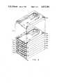
- FIG. 9shows an array of antenna elements of FIG. 2.
- a multibeam radio frequency antenna system 10is shown to include to include a radio frequency lens 12 having a plurality of feed ports 14a-14n disposed along a portion of the periphery of such lens 12 and a plurality of, here eight array ports 16 1 -16 8 disposed along an opposing portion of the periphery of the lens 12, the plurality of array ports 16 1 -16 8 being coupled to an array 20 of a plurality of, here eight, identically constructed antenna elements 20 1 -20 8 through a power distribution network 24, the details of which will be described hereinafter.
- the shape of the lens 12, the construction of the power distribution network 24 and the arrangement of the antenna elements 20 1 -20 8are selected such that n collimated beams of radio frequency energy are formed in free space, each one of such n beams having a different direction and each one of such n beams having circularly polarized radio frequency energy.
- antenna element 20 1an exemplary one of the plurality of identically constructed antenna elements 20 1 -20 8 , here antenna element 20 1 , is shown in detail to include a pair of substantially identically (except for the front edges for reasons to be described hereinafter) constructed conductive members 22 1 , 22 2 .
- the post 23 of the upper tapered ridge 25 formed on the bottom plate 27 1 of member 22 1is disposed within the aperture 28 formed on the lower tapered ridge 29 formed on the upper surface of bottom plate 27 2 of member 22 1 (FIGS.
- a rectangular cross-section, waveguideis formed having an open front end and a rearward, double ridge feed fed via coaxial connector 31 as described in our U.S. Pat. No. 4,353,074, entitled "Radio Frequency Ridged Waveguide Antenna", issued Oct. 5, 1982, and assigned to the same assignee as the present invention.
- Such formed waveguideis thus adapted to transmit and/or receive radio frequency energy having a linear polarization with the electric field thereof in the E-plane, i.e., in a vertical plane perpendicular to the planes of the plates 27 1 , 27 2 of members 22 1 , 22 2 which form the opposing wide walls of the waveguide, as shown by the vector E 1 in FIG. 1.
- Slots 24a, 24bare formed in the sidewalls 28a, 28b of member 22 2 .
- the formed slots 24a, 24bare disposed midway between the top surface portions 21 of member 22 2 and the upper surface portion of bottom plate 27 2 of member 22 2 .
- a planar microstrip circuit 26Disposed within slots 24a, 24b formed in the frontal portion of the opposing narrow sidewalls 28a, 28b of member 22 2 is a planar microstrip circuit 26, here a strip transmission line circuit having a plurality of, here four, flared notch-shaped antenna elements 30a-30d similar to that described in U.S. Pat. No.
- 4,353,072for providing radio frequency energy having a linear polarization with the electric field thereof disposed in the H-plane (i.e., horizontal) of the waveguide (as described in U.S. Pat. No. 4,353,072) and having a phase center midway between the sidewalls 28a, 28b of the formed waveguide as shown by the vector E 2 in FIG. 1.
- the microstrip circuit 26is also fed through a feed structure 32 similar to that described in U.S. Pat. No. 4,353,072. It is noted that here, however, such microstrip circuit 26 is fed by a feed structure 32 which feeds energy through one of the sidewalls 28a, 28b (here the left sidewall 28a) via a coaxial connector 33.
- planar microstrip circuit 26is disposed in a plane positioned midway between the upper and lower opposing widewalls of the formed waveguide.
- the phase center of the horizontally polarized energy provided by the strip transmission line circuit 26is a vertical plane, symmetrically disposed between the upper and lower opposing wide walls of the formed waveguide.
- the phase center of the vertically polarized energy provided by the double ridges 25, 29is also midway between the opposing upper and lower wide walls 27 1 , 27 2 .
- the double ridges 25, 29are disposed midway between the narrow sidewalls 28a, 28b.
- the vertically polarized radio frequency energy provided by the double ridge fed waveguide formed by the pair of conductive members 22 1 , 22 2 and the horizontally polarized radio frequency energy provided by the microwave circuit 26have coincident phase centers at point P, such point being at the center of the front end of the formed waveguide as shown in FIG. 1.
- antenna element 20 1produces circularly polarized radio frequency energy.
- the power distribution network 24includes a plurality of, here eight, quadrature hybrid couplers 40 1 -40 8 , each having a pair of input terminal 42 1 , 44 1 to 42 8 , 44 8 and a pair of output terminals 46 1 , 48 1 to 46 8 , 48 8 .
- One of the pair of input terminals 42 1 -42 8is coupled to a corresponding one of the array ports 16 1 -16 8 , as shown, and the other one of the pair of input terminals 44 1 -44 8 is terminated in a matched 1oad 49, as shown.
- power fed to the couplers 40 1 -40 8is divided equally between a pair of output ports 46 1 , 48 1 to 46 8 , 48 8 , but the signals at the output ports 46 1 -46 8 differ in phase from the signals at output ports 48 1 -48 8 by ninety degrees.
- the output ports 46 1 -46 8are fed to the coxial axial connectors 31 of elements 20 1 -20 8 , respectively, and hence to the double ridge feeds of the waveguide and the output ports 48 1 -48 8 are fed to the coaxial connectors 33 of elements 20 1 -20 8 , respectively, and hence to the microstrip circuits 26 to thereby provide the desired 90 degree relative phase shift between the signal fed to the double ridge feed at the rear end of the formed waveguides and the signal fed to the microwave circuits and thus enable production of the desired circularly polarized radio frequency energy.
- each one of such members 22 1 , 22 2is constructed from a block of electrically conductive material, here aluminum.
- the upper surface 21 of such blockhas machined therein S-shaped side walls 28a, 28b and a rear wall portion 58 has a recess or notch 60 formed therein.
- Also machined into the upper surface 21 of the members 22 1 , 22 2is the tapered ridge 29, as shown.
- the tapered ridge 29has aperture 28 formed in the upper, flat top portion thereof, the flat top portion terminating in a tapered portion, as shown.
- Member 22 2also has slots 24a, 24b machined into the side walls 28a, 28b thereof. Such slots 24a, 24b are, as described above, midway between the upper surface of the bottom plate 27 2 of member 22 2 and the bottom surface of the bottom plate 27 1 of member 22 1 . Disposed along the curved regions of the side walls 28a, 28b are open ended channels 70, 72.
- Channels 70, 72are here formed of curved conductive strips 74, 76, here aluminum having ends 78, 80 spaced from, and affixed to side walls 28a, 28b respectively.
- the spacingis provided by aluminum spacers 82, 84, such ends 78, 80 and spacers 82, 84 being affixed to the side wall portions through a convenient means as by bolts or a suitable electrically conductive epoxy, not shown.
- the channels 70, 72are effective in removing unwanted surface currents produced along the side walls 28a, 28b, as described in the above-referenced U.S. Pat. No. 4,353,074.
- the side walls 28a, 28b disposed between the tapered ridge 29 and the frontal end of the member 22 2are flared outwardly along a nonlinear path to increase the surface length of the side walls 28a, 28b from the tapered ridge 29 to free space within the fixed longitudinal length of the antenna element 22 1 thereby providing a relatively compact antenna element with a side wall length sufficiently long to provide an adequate transition region between the tapered ridge and free space. It is noted that while the left hand portion 90 of the bottom plate 27 2 of member 22 2 extends to the front end of the left side wall 28a, the right hand portion 92 of the bottom plate 27 2 terminates a predetermined distance from the front end of the right side wall 28b.
- the front edge 95 of the bottom plate 27 2is disposed at an angle A with respect to such dotted line 93.
- the right end 100 of the bottom plate 27 1extends to the end of the right side wall 28b of member 22 1 while the left end 102 of the bottom plate 27 1 is foreshortened.
- the front edge 106 of bottom plate 27 1makes also an acute angle A with respect to the dotted line 108 passing through the ends of the side walls 28a, 28b of the upper memeber 27 1 .
- the frontal portion of the formed waveguideappears as shown in FIG. 4; that is, the front edges 95, 106 of the bottom plates 27 1 , 27 2 forming the upper and lower side walls of the waveguide cross one another at a point X in the center of the waveguide so that the front portions 90, 100 of the wide walls are neither underlayed nor overlayed with a wide wall of the formed waveguide. More particularly, the right hand portion 100 (in FIG. 4) of the upper wide wall 27 1 is not overlayed by the lower wide wall 27 2 and the left hand portions 90 of the lower wide wall 27 2 is not underlayed by the upper wide wall 27 1 .
- the degree of non-overlappingis a function of the shape of the edges 95, 106 and such is selected to provide a match between the antenna gain of the double-ridge fed waveguide portion of the antenna element and the antenna gain of the microstrip circuit antenna element; i.e., a match in gain between the horizontal and vertical polarization components of the radio frequency energy. More specifically, this allows the microstrip circuit gain to increase to the same level as the waveguide gain and closely follow the waveguide gain over the frequency band and over a field of view of approximately 90°. The gain of the waveguide is approximately the same as it would have been if the bottom plates 27 1 , 27 2 were not foreshorted. It is noted that the left sidewall 28a (FIG. 2) of member 22 2 is provided with a slot 61 which is used to accept a feed structure for the microwave circuit 26 (FIG. 2) and a portion of connector 33. Such slot 61 will be described in more detail hereinafter.
- the bottom surface of bottom plate 27 1 of member 22 1has the tapered ridge 25 formed thereon.
- the flat portion of the ridge 25has the turret shaped conductive post 23 press fit therein by a pin shaped end as described in U.S. Pat. No. 4,353,074 referred to above.
- Post 23has a hole drilled therein for receiving the center conductor 92 (FIG. 2) of the coaxial connector 31 as described in U.S. Pat. No. 4,353,074. It is noted from FIGS. 2, 3 and 6 that the tapered ridges 25, 27 formed on the upper and lower surfaces of member 22 1 are in alignment or registration with each other. Further, it is evident that the post 23 of member 22 1 fits into the aperture 28 of member 26 2 as shown and as described in detail in U.S. Pat. No. 4,353,074.
- each one of the dielectric support structures 110, 112has a sheet of conductive material, here copper clad on the upper and lower surfaces thereof.
- the sheet of conductive material on the lower surface of upper dielectric support structure 110is removed entirely with a suitable chemical etchant whereas a plurality of here, four flared notches 120a-120b symmetrically disposed with respect to the edges 122a, 122b are etched into the conductive material 114 clad onto the upper surface of such upper dielectric support structure 110 using conventional photolithographic-chemical etching techniques.
- Each one of the notches 120a-120dhas a narrow portion 124 and a wider portion 126.
- the notches 120 a-120dare separated from each other a distance less than a half wavelength at the smallest operating wavelength of the antenna.
- a pair of slots 130a, 130bdisposed a predetermined distance from the side edges 122a, 122b of the support 110. The distance is selected so that when circuit 26 is inserted into slots 24a, 24b (FIG. 2), the inner surfaces 111a, 111b of the sidewalls 28a, 28b are in the middle of the slots 122a, 122b (FIG. 5) particularly in the region when circuit 26 is fed via connector 33.
- a similar pattern of four flared notches 140a-140dis etched into the conductive sheet 144 clad to the bottom surface of such dielectric support structure 112.
- Each one of the notches 140a-140dis identical to the notches 120a-120d formed on the conductive sheet 114 clad to the upper surface of dielectric support 110. Also etched in the conductive sheet 148a, 148b is a pair of slots spaced the same predetermined distance from the sides 150a, 150b of the support 112 as slots 130 a, 130b. The conductive sheet initially clad to the upper surface of the dielectric support structure 112 is etched to form a feed network 32.
- the feed network 32is a strip transmission line circuit having strip conductor 152 disposed between a pair of ground plane conductors formed by the conductive sheets 114, 144, (except for the region 155 where the portion 152a of strip conductor 152 passes through slots 130a, 148a (FIG. 8)) and separated from such sheets 114, 144 by the dielectric support structures 110, 112.
- the feed network 32includes a first two-to-one power divider section 154 the output of which in turn feeds a pair of two-to-one power divider sections 156, 158.
- Each one of the three power divider sections 154, 156, 158includes a step-matching transformer section 160.
- each feed line 162a-162dis disposed underneath the narrow portions 124 of notches 120a-120d and hence the narrow portions of elements 30a-30d, as shown in FIG. 5, because the notches 120a-120d in conductive sheet 114 being in registration with notches 140a-140d formed in conductive sheet 144 form such flared notched antenna elements 30a-30d.
- the pair of slots 130a, 130bare also aligned over slots 148a, 148b, respectively).
- strip conductor 152 fed to the two-to-one power divider 154extends towards, and exits from the left edges 122 a, 150a of the circuit. It is also noted that as the portion 152a of strip conductor 152 passes between the pair of slots 122a, 148a (i.e., through region 155) formed in the upper and lower ground planes 114, 144 of the strip transmission line circuit 26, such strip conductor portion 152a is without upper and lower ground planes.
- the slots 122a, 122b, 148a, 148bare formed in the upper and lower ground planes of the strip transmission line circuit so that the inner regions 114a, 144a of the ground planes 114, 144 are dielectrically separated (via substrates 110, 112) from outer regions 114b, 144b and when the circuit 26 is inserted into the slots 24a, 24b formed in the side walls of member 22 2 (FIG. 2), the ground planes of the strip transmission line circuit 26 formed by sheets 114, 144 are insulated from the conductive side walls 28a, 28b by the dielectric of substrates 110, 112. It is noted that the back walls 151a, 151b (FIGS.
- slots 24a, 24bprevent the back edge 153 of circuit 26 from contacting the spacers 82, 84 and strips 74, 76. More particularly, by merely placing the microwave circuit 26 midway between the upper and lower wide walls of the formed waveguide and with the upper and lower ground planes of the microwave circuit of feed 32 in contact with the narrow side walls 28a, 28b, a gain drop in the waveguide portion was experienced and the bandwidth was limited to about one octave. But, with the ground planes of feed 32 isolated from the narrow side walls 28a, 28b, the gain drop out was substantially removed. However, in order to provide ground planes above and below the strip conductor portion 152a, a pair of dielectric slabs 180, 182 (FIGS.
- upper dielectric slab 180has copper 184 clad to the upper surface thereof and lower dielectric slab 182 has copper 186 clad to the bottom surface thereof.
- the left bottom portion (FIGS. 2 and 8) of slab 182rests on a flat region 190 formed in conductive member 22 2 .
- the dielectric slabs 180, 182bridge the slots 130a, 148a formed in the ground planes 114, 144 of the feed 32 of microstrip circuit 26 and the copper 184, 186 clad to the upper and lower surfaces of the slabs 180, 182, respectively, provide a continuous (albeit elevated) ground plane for the strip conductor portion 152a.
- the slabs 180, 182are held into place by a conductive cap 191, as indicated. More particularly, the bottom of cap 191 has a recess 193 for receiving the top, copper 184 clad portion of slab 180. It is also noted that a groove 195 (FIG. 2) is formed in a flat section 196 for receiving the front portions of connector 33.
- cap 191is shaped so that a left wall 197 of slot 193 contacts the left portion of the copper 184 on slab 180 and to also contact the left edge of the outer portion 114b of clad copper 114.
- the sidewall 22 2is shaped (FIG. 8) so that the back wall 189 of flat 190 makes contact with the left portion of the copper 186 clad to the bottom of slab 182 and also to contact the outer portion 144b of the clad copper 144.
- a coaxial cable connector 33has the center conductor 192 connected to the left end of the strip conductor portion 152a and the insulated (via hole 195) outer conductor 154 of such connector 33 is electrically connected to conductive mounting block 192 and member 22 2 and hence to the copper 184, 186 clad to the upper and lower slabs 180, 182 and to the outer portions 114b, 144b of clad copper 114, 144.
- the copper 184, 186 clad to the slabs 180, 182thus bridge slots 130a, 148a to provide a continuous, elevated, ground plane for the strip conductor portions 152a but the ground planes (i.e., the inner portions 114a, 144a of the clad copper 114, 144 (FIG.
- the energy radiated by the notchesis linearly polarized; more particularly, here horizontally polarized.
- a gap 170is formed between the flat portions of the tapered ridges 25, 29, as described in U.S. Pat. No. 4,353,074. This gap 170 is used to establish a vertical electric field E 1 . It is noted that gap 170 is disposed along the coaxial center line 171 of the waveguide.
- the plane of the microwave circuit 26is disposed in alignment with the gap 170, that is, the plane of circuit 26 is parallel to bottom plates 27 1 , 27 2 and is also disposed along the axial center line 171 of the waveguide, i.e., in line with the gap 170.
- the electric field E2 produced by circuit 26 and the field E 1 produced by the gap 170 in the formed waveguideare coincident and in the center of the formed waveguide.
- conductive members 22 3 , 22 5 , 22 7 , 22 9are identical to conductive member 22 1 (including the front edges 106 thereof) and conductive members 22 4 , 22 6 , 22 8 ) are identical to conductive member 22 2 (including the front edges 95 thereof).
- Each of the microwave circuits 26 at each one of the elements 20 1 -20 8is identical.
- edges 95, 106are linear, other shapes may be used. It is felt, therefore, that the invention should not be restricted to the described embodiment, but rather should be limited only by the spirit and scope of the appended claims.
Landscapes
- Waveguide Aerials (AREA)
Abstract
Description
This invention relates generally to radio frequency antenna and more particularly to radio frequency antenna adapted to operate with circular polarization.
As is known in the art, it is frequently desirable to provide a radio frequency antenna adapted to operate with circular polarization. One such antenna is described in U.S. Pat. No. 4,353,072, entitled "Circularly Polarized Radio Frequency Antenna", issued Oct. 5, 1982, inventor George J. Monser and assigned to the same assignee as the present invention. As described therein, the radio frequency antenna includes an antenna element having a forward, open-ended waveguide section, the upper and lower relatively wide side walls thereof being provided by the ground planes of a pair of microwave circuits. A first feed is disposed adjacent the rearward end of the waveguide section for radiating radio frequency energy having an electric field normal to the upper and lower wide walls of the waveguide section (i.e., a vertical polarization having a phase center at the center of the open-ended waveguide). Each one of the pair of microwave circuits includes a strip transmission line circuit having disposed adjacent the forward, open-ended waveguide section an array of radiating elements and a rearward feed for radiating from the array of radiating elements radio frequency energy having an electric field parallel to the plane of the upper and lower side walls (i.e., a horizontal polarization). Thus, by feeding equal, in-phase signals to the pair of microwave circuits and by feeding a 90° phase shifted signal to the first feed, circularly polarized energy is radiated by the antenna element. Further, with such arrangement, the resultant phase center of the horizontally polarized energy is disposed at the center of the open-ended waveguide and, therefore, both the horizontal and vertical polarization components have coincident phase centers. While such antenna element does provide circular polarization, when used in relatively large arrays, a relatively large power distribution network is required to feed equal signals to each of the pair of microwave circuits of each of the antenna elements in the array. Further, such network may add loss and unwanted phase shift which with increasing scan angles, leads to non-coincident phase center and reduced quality of the circular polarization.
In accordance with the present invention, a radio frequency antenna is provided comprising: a waveguide section; first means for establishing radio frequency energy in such waveguide section having a first linear polarization with an electric field disposed normal to opposing wide walls of the waveguide section; a planar microwave circuit means, for establishing a second linear polarization having an electric field disposed perpendicular to the electric field of the first linear polarization, such microwave circuit means being disposed within the waveguide between the wide walls and relative to the feed means to provide the first linear polarization and the second linear polarization with substantially coincident phase centers.
In a preferred embodiment of the invention, the microwave circuit means includes a strip conductor feed separated from a ground plane conductor by a dielectric, such ground plane conductor having a notch formed therein and fed by the strip conductor. More particularly, the dielectric is a planar sheet of dielectric material having the ground plane conductor formed on one surface thereof and the strip conductor feed formed on the other surface thereof. The first feed means launches the first linearly polarized energy with the electric field disposed in the E-plane of the waveguide and the planar dielectric sheet is disposed in the H-plane of the waveguide. The first feed means and the strip line feed are feed signals having a ninety degree phase shift therebetween. With such arrangement, a relatively simple feed structure is provided.
In accordance with an additional feature of the invention, the ground plane of the microwave circuit is dielectrically spaced from the narrow side walls of the waveguide. The strip conductor of the microwave circuit passes through one of the sidewalls of the waveguide and such portion of the strip conductor is provided with a ground plane dielectrically spaced from the ground plane of the microwave circuit to maintain the dielectric separation between the sidewalls and the ground plane of the microwave circuit.
In accordance with a further additional feature of the invention, the front ends of the upper and lower wide walls of the waveguide have non-overlaying regions to provide a balance between the gain of the waveguide and the gain of the microwave circuit.
The foregoing features of this invention, as well as the invention itself, may be more fully understood from the following description read together with the accompanying drawings in which:
FIG. 1 is a schematic diagram of a radio frequency antenna system including an array of antenna elements according to the invention;
FIG. 2 is an exploded isometric drawing, partly broken away, of an exemplary one of the antenna elements in the array of FIG. 1;
FIG. 3 is an exploded isometric view of a pair of adjacent conductive members which, when affixed to each other, form an open-ended, double ridge fed waveguide portion of the antenna element of FIG. 2;
FIG. 4 is a top plan view of the front portion of the open-ended waveguide formed by the affixed conductive members of FIG. 3;
FIG. 5 is a top plan view of the bottom one of the pair of conductive members of FIG. 3;
FIG. 6 is an exploded cross-sectional side elevation. view of the antenna element of FIG. 2 formed by the pair of conductive members of FIG. 3, such cross-section being taken along the longitudinal center line of the waveguide formed by the affixed pair of members;
FIG. 6A is a cross-sectional view showing a portion of the antenna element of FIG. 2 when the pair of conductive members of FIG. 2 are mounted together and with the feed network of FIG. 7 disposed within such antenna element, such portion being ofregion 6A--6A of FIG. 6;
FIG. 7 is an exploded, isometric view of a strip transmission line feed network used in the antenna element of FIG. 2;
FIG. 8 is a perspective view partially broken away and showing in cross-section, a portion of the lower conductive member of FIG. 3 affixed to the strip transmission line feed network of FIG. 7, such view showing the connection of the strip transmission line circuit to a coaxial connector; and
FIG. 9 shows an array of antenna elements of FIG. 2.
Referring now to FIG. 1, a multibeam radio frequency antenna system 10 is shown to include to include aradio frequency lens 12 having a plurality of feed ports 14a-14n disposed along a portion of the periphery ofsuch lens 12 and a plurality of, here eight array ports 161 -168 disposed along an opposing portion of the periphery of thelens 12, the plurality of array ports 161 -168 being coupled to anarray 20 of a plurality of, here eight, identically constructed antenna elements 201 -208 through a power distribution network 24, the details of which will be described hereinafter. Suffice it to say here, however, that the shape of thelens 12, the construction of the power distribution network 24 and the arrangement of the antenna elements 201 -208 are selected such that n collimated beams of radio frequency energy are formed in free space, each one of such n beams having a different direction and each one of such n beams having circularly polarized radio frequency energy.
Referring now to FIG. 2, an exemplary one of the plurality of identically constructed antenna elements 201 -208, hereantenna element 201, is shown in detail to include a pair of substantially identically (except for the front edges for reasons to be described hereinafter) constructedconductive members bottom plate 271 ofmember 221 is disposed on thetop surface 21 ofmember 222, thepost 23 of the uppertapered ridge 25 formed on thebottom plate 271 ofmember 221 is disposed within theaperture 28 formed on the lowertapered ridge 29 formed on the upper surface ofbottom plate 272 of member 221 (FIGS. 3 and 6) a rectangular cross-section, waveguide is formed having an open front end and a rearward, double ridge feed fed viacoaxial connector 31 as described in our U.S. Pat. No. 4,353,074, entitled "Radio Frequency Ridged Waveguide Antenna", issued Oct. 5, 1982, and assigned to the same assignee as the present invention. Such formed waveguide is thus adapted to transmit and/or receive radio frequency energy having a linear polarization with the electric field thereof in the E-plane, i.e., in a vertical plane perpendicular to the planes of theplates members Slots sidewalls member 222. The formedslots top surface portions 21 ofmember 222 and the upper surface portion ofbottom plate 272 ofmember 222. Disposed withinslots narrow sidewalls member 222 is aplanar microstrip circuit 26, here a strip transmission line circuit having a plurality of, here four, flared notch-shaped antenna elements 30a-30d similar to that described in U.S. Pat. No. 4,353,072 for providing radio frequency energy having a linear polarization with the electric field thereof disposed in the H-plane (i.e., horizontal) of the waveguide (as described in U.S. Pat. No. 4,353,072) and having a phase center midway between thesidewalls microstrip circuit 26 is also fed through afeed structure 32 similar to that described in U.S. Pat. No. 4,353,072. It is noted that here, however,such microstrip circuit 26 is fed by afeed structure 32 which feeds energy through one of thesidewalls left sidewall 28a) via acoaxial connector 33. It is also noted that here theplanar microstrip circuit 26 is disposed in a plane positioned midway between the upper and lower opposing widewalls of the formed waveguide. Thus, the phase center of the horizontally polarized energy provided by the striptransmission line circuit 26 is a vertical plane, symmetrically disposed between the upper and lower opposing wide walls of the formed waveguide. Further, the phase center of the vertically polarized energy provided by thedouble ridges wide walls double ridges narrow sidewalls conductive members microwave circuit 26 have coincident phase centers at point P, such point being at the center of the front end of the formed waveguide as shown in FIG. 1. Thus, by feeding signals to the formed double ridge fed waveguide and the microwave circuit with equal power and with a π/2 radian phase shift therebetween,such antenna element 201 produces circularly polarized radio frequency energy.
Referring again to FIG. 1, such power division and phase shifting is provided by the power distribution network 24. The power distribution network 24 includes a plurality of, here eight, quadrature hybrid couplers 401 -408, each having a pair of input terminal 421, 441 to 428, 448 and a pair ofoutput terminals 461, 481 to 468, 488. One of the pair of input terminals 421 -428 is coupled to a corresponding one of the array ports 161 -168, as shown, and the other one of the pair of input terminals 441 -448 is terminated in a matched1oad 49, as shown. Hence, power fed to the couplers 401 -408 is divided equally between a pair ofoutput ports 461, 481 to 468, 488, but the signals at the output ports 461 -468 differ in phase from the signals at output ports 481 -488 by ninety degrees. The output ports 461 -468 are fed to the coxialaxial connectors 31 of elements 201 -208, respectively, and hence to the double ridge feeds of the waveguide and the output ports 481 -488 are fed to thecoaxial connectors 33 of elements 201 -208, respectively, and hence to themicrostrip circuits 26 to thereby provide the desired 90 degree relative phase shift between the signal fed to the double ridge feed at the rear end of the formed waveguides and the signal fed to the microwave circuits and thus enable production of the desired circularly polarized radio frequency energy.
Referring now in more detail to FIG. 3, each one ofsuch members upper surface 21 of such block has machined therein S-shaped side walls rear wall portion 58 has a recess ornotch 60 formed therein. Also machined into theupper surface 21 of themembers ridge 29, as shown. The taperedridge 29 hasaperture 28 formed in the upper, flat top portion thereof, the flat top portion terminating in a tapered portion, as shown. It is noted that the separation between the opposingnarrow side walls ridge 29 is relatively constant, however, such separation decreases, here along a curved paths, as such rear wall portions extend towards therear wall 58.Member 222 also hasslots side walls Such slots bottom plate 272 ofmember 222 and the bottom surface of thebottom plate 271 ofmember 221. Disposed along the curved regions of theside walls channels Channels conductive strips side walls aluminum spacers spacers channels side walls
Theside walls tapered ridge 29 and the frontal end of themember 222 are flared outwardly along a nonlinear path to increase the surface length of theside walls ridge 29 to free space within the fixed longitudinal length of theantenna element 221 thereby providing a relatively compact antenna element with a side wall length sufficiently long to provide an adequate transition region between the tapered ridge and free space. It is noted that while theleft hand portion 90 of thebottom plate 272 ofmember 222 extends to the front end of theleft side wall 28a, theright hand portion 92 of thebottom plate 272 terminates a predetermined distance from the front end of theright side wall 28b. Thus, while the front ends of the opposingside walls line 93, thefront edge 95 of thebottom plate 272 is disposed at an angle A with respect to such dottedline 93. Further, considering thebottom plate 271 ofmember 221, it is noted that theright end 100 of thebottom plate 271 extends to the end of theright side wall 28b ofmember 221 while theleft end 102 of thebottom plate 271 is foreshortened. Thus, thefront edge 106 ofbottom plate 271 makes also an acute angle A with respect to the dottedline 108 passing through the ends of theside walls upper memeber 271. Thus, referring to FIG. 4, when the upper and lowerconductive members front edges bottom plates front portions wide wall 271 is not overlayed by the lowerwide wall 272 and theleft hand portions 90 of the lowerwide wall 272 is not underlayed by the upperwide wall 271. The degree of non-overlapping is a function of the shape of theedges bottom plates left sidewall 28a (FIG. 2) ofmember 222 is provided with aslot 61 which is used to accept a feed structure for the microwave circuit 26 (FIG. 2) and a portion ofconnector 33.Such slot 61 will be described in more detail hereinafter.
Referring again to FIG. 3, the bottom surface ofbottom plate 271 ofmember 221 has the taperedridge 25 formed thereon. The flat portion of theridge 25 has the turret shapedconductive post 23 press fit therein by a pin shaped end as described in U.S. Pat. No. 4,353,074 referred to above.Post 23 has a hole drilled therein for receiving the center conductor 92 (FIG. 2) of thecoaxial connector 31 as described in U.S. Pat. No. 4,353,074. It is noted from FIGS. 2, 3 and 6 that the taperedridges member 221 are in alignment or registration with each other. Further, it is evident that thepost 23 ofmember 221 fits into theaperture 28 ofmember 262 as shown and as described in detail in U.S. Pat. No. 4,353,074.
Referring now to FIG. 7, an exemplary one of the identically constructed striptransmission line circuits 26 used in each one of the antenna elements 201 -208 (FIG. 1), here the one used inelement 201, is shown in detail to include a pair of planar dielectric support structures orsubstrates dielectric support structures dielectric support structure 110 is removed entirely with a suitable chemical etchant whereas a plurality of here, four flared notches 120a-120b symmetrically disposed with respect to theedges conductive material 114 clad onto the upper surface of such upperdielectric support structure 110 using conventional photolithographic-chemical etching techniques. Each one of the notches 120a-120d has anarrow portion 124 and awider portion 126. The notches 120 a-120d are separated from each other a distance less than a half wavelength at the smallest operating wavelength of the antenna. Also etched in theconductive material 114 are a pair ofslots support 110. The distance is selected so that whencircuit 26 is inserted intoslots sidewalls slots circuit 26 is fed viaconnector 33. Considering now the second one of the pair of dielectric support structure 112 a similar pattern of four flared notches 140a-140d is etched into theconductive sheet 144 clad to the bottom surface of suchdielectric support structure 112. Each one of the notches 140a-140d is identical to the notches 120a-120d formed on theconductive sheet 114 clad to the upper surface ofdielectric support 110. Also etched in theconductive sheet support 112 asslots dielectric support structure 112 is etched to form afeed network 32. Thefeed network 32 is a strip transmission line circuit havingstrip conductor 152 disposed between a pair of ground plane conductors formed by theconductive sheets region 155 where theportion 152a ofstrip conductor 152 passes throughslots such sheets dielectric support structures feed network 32 includes a first two-to-onepower divider section 154 the output of which in turn feeds a pair of two-to-onepower divider sections power divider sections transformer section 160. Thus, power fed to the strip transmissionline feed network 32 is divided equally, and in phase, to each one of fourfeed lines 162a-162d. Eachfeed line 162a-162d is disposed underneath thenarrow portions 124 of notches 120a-120d and hence the narrow portions of elements 30a-30d, as shown in FIG. 5, because the notches 120a-120d inconductive sheet 114 being in registration with notches 140a-140d formed inconductive sheet 144 form such flared notched antenna elements 30a-30d. (It is also noted that the pair ofslots slots strip conductor 152 fed to the two-to-onepower divider 154 extends towards, and exits from theleft edges 122 a, 150a of the circuit. It is also noted that as theportion 152a ofstrip conductor 152 passes between the pair ofslots transmission line circuit 26, suchstrip conductor portion 152a is without upper and lower ground planes. Theslots inner regions 114a, 144a of the ground planes 114, 144 are dielectrically separated (viasubstrates 110, 112) fromouter regions circuit 26 is inserted into theslots transmission line circuit 26 formed bysheets conductive side walls substrates slots back edge 153 ofcircuit 26 from contacting thespacers microwave circuit 26 midway between the upper and lower wide walls of the formed waveguide and with the upper and lower ground planes of the microwave circuit offeed 32 in contact with thenarrow side walls feed 32 isolated from thenarrow side walls strip conductor portion 152a, a pair ofdielectric slabs 180, 182 (FIGS. 2 and 6) havingcopper 184, 186 (FIGS. 6 and 8) clad on one surface thereof is provided. More particularly, upperdielectric slab 180 hascopper 184 clad to the upper surface thereof and lowerdielectric slab 182 hascopper 186 clad to the bottom surface thereof. The left bottom portion (FIGS. 2 and 8) ofslab 182 rests on aflat region 190 formed inconductive member 222. Thus, referring to FIGS. 2 and 8, thedielectric slabs slots feed 32 ofmicrostrip circuit 26 and thecopper slabs strip conductor portion 152a. Theslabs conductive cap 191, as indicated. More particularly, the bottom ofcap 191 has arecess 193 for receiving the top,copper 184 clad portion ofslab 180. It is also noted that a groove 195 (FIG. 2) is formed in aflat section 196 for receiving the front portions ofconnector 33. It is noted thatcap 191 is shaped so that aleft wall 197 ofslot 193 contacts the left portion of thecopper 184 onslab 180 and to also contact the left edge of theouter portion 114b of cladcopper 114. Further, thesidewall 222 is shaped (FIG. 8) so that theback wall 189 of flat 190 makes contact with the left portion of thecopper 186 clad to the bottom ofslab 182 and also to contact theouter portion 144b of the cladcopper 144. Thus, acoaxial cable connector 33 has the center conductor 192 connected to the left end of thestrip conductor portion 152a and the insulated (via hole 195)outer conductor 154 ofsuch connector 33 is electrically connected to conductive mounting block 192 andmember 222 and hence to thecopper lower slabs outer portions copper copper slabs bridge slots strip conductor portions 152a but the ground planes (i.e., theinner portions 114a, 144a of the cladcopper 114, 144 (FIG. 7)) of thefeed 32 of the striptransmission line circuit 26 are dielectrically spaced (i.e., isolated) from thenarrow sidewall 28a, thus substantially removing any gain drop out which would have resulted by not havingslots copper dielectric slabs feed 32. When strip transmissionline feed network 26 is fed radio frequency energy from a coaxial connector 33 (FIG. 8), the striptransmission line circuit 26 couples energy to the notched antenna elements 30a-30d whereupon such feed energy is then radiated into free space with an electric field vector disposed in the plane of the striptransmission line circuit 26 as shown by the vector E2 in FIG. 1. Thus, the energy radiated by the notches is linearly polarized; more particularly, here horizontally polarized. It is also noted from FIGS. 6 and 6A that when thebottom plate 271 rests ontop surface 21 of member 222 agap 170 is formed between the flat portions of the taperedridges gap 170 is used to establish a vertical electric field E1. It is noted thatgap 170 is disposed along thecoaxial center line 171 of the waveguide. It is also noted that the plane of themicrowave circuit 26 is disposed in alignment with thegap 170, that is, the plane ofcircuit 26 is parallel tobottom plates axial center line 171 of the waveguide, i.e., in line with thegap 170. Thus, the electric field E2 produced bycircuit 26 and the field E1 produced by thegap 170 in the formed waveguide are coincident and in the center of the formed waveguide.
Referring now to FIG. 9, thearray 20 of the antenna element 201 -208 is shown. It is noted thatconductive members front edges 106 thereof) andconductive members front edges 95 thereof). Each of themicrowave circuits 26 at each one of the elements 201 -208 is identical.
Having described a preferred embodiment of the invention, it is now evident that other embodiments incorporating these concepts may be used. Thus, for example, while theedges
Claims (13)
1. A radio frequency antanna comprising:
(a) a waveguide section comprising a pair of opposing, relatively wide walls and a pair of opposing, relatively narrow side walls;
(b) first feed means for establishing radio frequency energy in such waveguide section having a first linear polarization with an electric field disposed normal to the opposing wide walls of the waveguide section; and
(c) a planar microwave circuit means, for establishing radio frequency energy having a second linear polarization with an electric field disposed perpendicular to the electric field of the first linear polarization, such microwave circuit means comprising a strip conductor feed separated from a ground plane conductor by a dielectric, said microwave circuit means being disposed within the waveguide section intermediately between the opposing, relatively wide walls thereof with the ground plane conductor of the planar microwave circuit means being dielectrically spaced from the pair of opposing, relatively narrow side walls.
2. The antenna recited in claim 1 wherein the ground plane conductor has a notch formed therein, said notch being fed by the strip conductor feed.
3. The antenna recited in claim 2 wherein the dielectric is a planar sheet of dielectric material having the ground plane conductor formed on one surface thereof and the strip conductor feed formed on the other surface thereof and wherein the first feed means launches the first linearly polarized energy with the electric field disposed in the E-plane of the waveguide and the planar dielectric sheet is disposed in the H-plane of the waveguide.
4. The antenna recited in claim 3 wherein a portion of the strip conductor feed of the planar microwave circuit means passes through one of the pair of relatively narrow side walls of the waveguide section, and wherein such portion of the strip conductor feed is provided with a ground plane dielectrically spaced from the ground plane of the planar microwave circuit means to maintain the dielectric separation between the pair of relatively narrow side walls and the ground plane of the planar microwave circuit means.
5. The antenna rected in claim 4 wherein front ends of the pair of opposing, relatively wide walls of the waveguide have non-overlaying regions.
6. A radio frequency antenna comprising:
(a) a waveguide section comprising a pair of opposing, relatively wide walls and a pair of opposing, relatively narrow side walls;
(b) first means, disposed in the waveguide section, for establishing radio frequency energy in such waveguide section having a first linear polarization with an electric field disposed normal to the opposing wide walls of the waveguide section; and
(c) second means, for establishing radio frequency energy having a second linear polarization with an electric field disposed perpendicular to the electric field of the first linear polarization, such second means comprising a microwave circuit including a strip conductor feed separated from a ground plane conductor by a dielectric, said second means being disposed within the waveguide section between the pair of opposing wide walls and relative to the first means to provide the radio frequency energy having the first linear polarization and the radio frequency energy having the second linear polarization with substantially coincident phase centers, said ground plane conductor being dielectrically spaced from the pair of opposing, relatively narrow side walls.
7. The antenna recited in claim 6 wherein the ground plane conductor has a notch formed therein fed by the strip conductor feed.
8. The antenna recited in claim 7 wherein the dielectric is a planar sheet of dielectric material having the ground plane conductor formed on one surface thereof and the strip conductor feed formed on the other surface thereof, and wherein the first means launches the first linearly polarized energy with the electric field thereof disposed in the E-plane of the waveguide and the planar dielectric sheet is disposed in the H-plane of the waveguide.
9. The antenna recited in claim 8 wherein a portion of the strip conductor feed of the microwave circuit passes through one of the pair of opposing, relatively narrow side walls of the waveguide section, and wherein such portion of the strip conductor feed is provided with a ground plane dielectrically spaced from the ground plane of the microwave circuit to maintain the dielectric separation between the pair of opposing, relatively narrow side walls and the ground plane of the microwave circuit.
10. The antenna recited in claim 6 wherein front ends of the pair of opposing, relatively wide walls of the waveguide section have non-overlaying regions.
11. A radio frequency antenna comprising:
(a) an electrically conductive waveguide section comprising a pair of opposing walls;
(b) feed means for establising ratio frequency energy in the waveguide section having a first linear polarization with an electric field disposed normal to the pair of opposing walls;
(c) microwave circuit means for establishing radio frequency energy in the waveguide section having a second linear polarization with an electric field disposed parallel to the pair of opposing walls, said microwave circuit means comprising a strip conductor circuit separated from a ground plane conductor by a dielectric, said microwave circuit means being disposed in the waveguide section intermediate the pair of opposing walls with the ground plane conductor being dielectrically separated from the electrically conductive waveguide section.
12. The radio frequency antenna of claim 11 wherein front ends of the pair of opposing walls of the waveguide section have non-overlaying regions.
13. In combination:
means for producing a pair of quadrature radio frequency signals; and
radio frequency antenna means, responsive to the pair of quadrature radio frequency signals, for producing circularly polarized radio frequency energy, said radio frequency antenna means comprising:
(i) electrically conductive waveguide means comprising a pair of opposing, relatively wide walls;
(ii) feed means, resonsive to a first one of the pair of quadrature radio frequency signals, for establishing radio frequency energy in the waveguide means having a first linear polarization with an electric field disposed normal to the opposing wide walls of the waveguide means; and
(iii) planar microwave circuit means, comprising a strip conductor feed separated from a ground plane conductor by a dielectric and fed by a second one of the pair of quadrature radio frequency signals, for establishing radio frequency energy having a second linear polarization with an electric field disposed perpendicular to the electric field of the first linear polarization, said microwave circuit means being disposed intermediate the pair of opposing, relatively wide walls with said ground plane conductor being dielectrically spaced from the waveguide means, said waveguide means producing circularly polarized radio frequency energy from the first linear polarization and the second linear polarization.
Priority Applications (1)
| Application Number | Priority Date | Filing Date | Title |
|---|---|---|---|
| US06/687,685US4672384A (en) | 1984-12-31 | 1984-12-31 | Circularly polarized radio frequency antenna |
Applications Claiming Priority (1)
| Application Number | Priority Date | Filing Date | Title |
|---|---|---|---|
| US06/687,685US4672384A (en) | 1984-12-31 | 1984-12-31 | Circularly polarized radio frequency antenna |
Related Child Applications (1)
| Application Number | Title | Priority Date | Filing Date |
|---|---|---|---|
| US07082948Continuation | 1987-08-05 |
Publications (1)
| Publication Number | Publication Date |
|---|---|
| US4672384Atrue US4672384A (en) | 1987-06-09 |
Family
ID=24761393
Family Applications (1)
| Application Number | Title | Priority Date | Filing Date |
|---|---|---|---|
| US06/687,685Expired - Fee RelatedUS4672384A (en) | 1984-12-31 | 1984-12-31 | Circularly polarized radio frequency antenna |
Country Status (1)
| Country | Link |
|---|---|
| US (1) | US4672384A (en) |
Cited By (155)
| Publication number | Priority date | Publication date | Assignee | Title |
|---|---|---|---|---|
| US4803495A (en)* | 1985-01-09 | 1989-02-07 | Raytheon Company | Radio frequency array antenna with energy resistive material |
| US4878061A (en)* | 1988-11-25 | 1989-10-31 | Valentine Research, Inc. | Broadband wide flare ridged microwave horn antenna |
| EP0434282A3 (en)* | 1989-12-21 | 1991-07-17 | Hughes Aircraft Company | Dual mode antenna apparatus having slotted waveguide and broadband arrays |
| US5175560A (en)* | 1991-03-25 | 1992-12-29 | Westinghouse Electric Corp. | Notch radiator elements |
| US5194875A (en)* | 1991-06-07 | 1993-03-16 | Westinghouse Electric Corp. | Notch radiator elements |
| US20080144689A1 (en)* | 2006-10-27 | 2008-06-19 | Raytheon Company | Power combining and energy radiating system and method |
| US20090153304A1 (en)* | 2007-12-17 | 2009-06-18 | Sands Daniel L | Side loaded shorted patch rfid tag |
| US20110102284A1 (en)* | 2009-11-04 | 2011-05-05 | Brown Kenneth W | Low Loss Broadband Planar Transmission Line To Waveguide Transition |
| US8478223B2 (en) | 2011-01-03 | 2013-07-02 | Valentine Research, Inc. | Methods and apparatus for receiving radio frequency signals |
| US9608740B2 (en) | 2015-07-15 | 2017-03-28 | At&T Intellectual Property I, L.P. | Method and apparatus for launching a wave mode that mitigates interference |
| US9615269B2 (en) | 2014-10-02 | 2017-04-04 | At&T Intellectual Property I, L.P. | Method and apparatus that provides fault tolerance in a communication network |
| US9628116B2 (en) | 2015-07-14 | 2017-04-18 | At&T Intellectual Property I, L.P. | Apparatus and methods for transmitting wireless signals |
| US9640850B2 (en) | 2015-06-25 | 2017-05-02 | At&T Intellectual Property I, L.P. | Methods and apparatus for inducing a non-fundamental wave mode on a transmission medium |
| US9667317B2 (en) | 2015-06-15 | 2017-05-30 | At&T Intellectual Property I, L.P. | Method and apparatus for providing security using network traffic adjustments |
| US9674711B2 (en) | 2013-11-06 | 2017-06-06 | At&T Intellectual Property I, L.P. | Surface-wave communications and methods thereof |
| US9685992B2 (en) | 2014-10-03 | 2017-06-20 | At&T Intellectual Property I, L.P. | Circuit panel network and methods thereof |
| US9692101B2 (en) | 2014-08-26 | 2017-06-27 | At&T Intellectual Property I, L.P. | Guided wave couplers for coupling electromagnetic waves between a waveguide surface and a surface of a wire |
| US9699785B2 (en) | 2012-12-05 | 2017-07-04 | At&T Intellectual Property I, L.P. | Backhaul link for distributed antenna system |
| US9705610B2 (en) | 2014-10-21 | 2017-07-11 | At&T Intellectual Property I, L.P. | Transmission device with impairment compensation and methods for use therewith |
| US9705561B2 (en) | 2015-04-24 | 2017-07-11 | At&T Intellectual Property I, L.P. | Directional coupling device and methods for use therewith |
| US9722318B2 (en) | 2015-07-14 | 2017-08-01 | At&T Intellectual Property I, L.P. | Method and apparatus for coupling an antenna to a device |
| US9729197B2 (en) | 2015-10-01 | 2017-08-08 | At&T Intellectual Property I, L.P. | Method and apparatus for communicating network management traffic over a network |
| US9735833B2 (en) | 2015-07-31 | 2017-08-15 | At&T Intellectual Property I, L.P. | Method and apparatus for communications management in a neighborhood network |
| US9742521B2 (en) | 2014-11-20 | 2017-08-22 | At&T Intellectual Property I, L.P. | Transmission device with mode division multiplexing and methods for use therewith |
| US9742462B2 (en) | 2014-12-04 | 2017-08-22 | At&T Intellectual Property I, L.P. | Transmission medium and communication interfaces and methods for use therewith |
| US9749053B2 (en) | 2015-07-23 | 2017-08-29 | At&T Intellectual Property I, L.P. | Node device, repeater and methods for use therewith |
| US9749013B2 (en) | 2015-03-17 | 2017-08-29 | At&T Intellectual Property I, L.P. | Method and apparatus for reducing attenuation of electromagnetic waves guided by a transmission medium |
| US9748626B2 (en) | 2015-05-14 | 2017-08-29 | At&T Intellectual Property I, L.P. | Plurality of cables having different cross-sectional shapes which are bundled together to form a transmission medium |
| US9762289B2 (en) | 2014-10-14 | 2017-09-12 | At&T Intellectual Property I, L.P. | Method and apparatus for transmitting or receiving signals in a transportation system |
| US9769128B2 (en) | 2015-09-28 | 2017-09-19 | At&T Intellectual Property I, L.P. | Method and apparatus for encryption of communications over a network |
| US9768833B2 (en) | 2014-09-15 | 2017-09-19 | At&T Intellectual Property I, L.P. | Method and apparatus for sensing a condition in a transmission medium of electromagnetic waves |
| US9769020B2 (en) | 2014-10-21 | 2017-09-19 | At&T Intellectual Property I, L.P. | Method and apparatus for responding to events affecting communications in a communication network |
| US9780834B2 (en) | 2014-10-21 | 2017-10-03 | At&T Intellectual Property I, L.P. | Method and apparatus for transmitting electromagnetic waves |
| US9787412B2 (en) | 2015-06-25 | 2017-10-10 | At&T Intellectual Property I, L.P. | Methods and apparatus for inducing a fundamental wave mode on a transmission medium |
| US9793951B2 (en) | 2015-07-15 | 2017-10-17 | At&T Intellectual Property I, L.P. | Method and apparatus for launching a wave mode that mitigates interference |
| US9793955B2 (en) | 2015-04-24 | 2017-10-17 | At&T Intellectual Property I, Lp | Passive electrical coupling device and methods for use therewith |
| US9793954B2 (en) | 2015-04-28 | 2017-10-17 | At&T Intellectual Property I, L.P. | Magnetic coupling device and methods for use therewith |
| US9800327B2 (en) | 2014-11-20 | 2017-10-24 | At&T Intellectual Property I, L.P. | Apparatus for controlling operations of a communication device and methods thereof |
| US9820146B2 (en) | 2015-06-12 | 2017-11-14 | At&T Intellectual Property I, L.P. | Method and apparatus for authentication and identity management of communicating devices |
| US9838896B1 (en) | 2016-12-09 | 2017-12-05 | At&T Intellectual Property I, L.P. | Method and apparatus for assessing network coverage |
| US9838078B2 (en) | 2015-07-31 | 2017-12-05 | At&T Intellectual Property I, L.P. | Method and apparatus for exchanging communication signals |
| US9847850B2 (en) | 2014-10-14 | 2017-12-19 | At&T Intellectual Property I, L.P. | Method and apparatus for adjusting a mode of communication in a communication network |
| US9847566B2 (en) | 2015-07-14 | 2017-12-19 | At&T Intellectual Property I, L.P. | Method and apparatus for adjusting a field of a signal to mitigate interference |
| US9853342B2 (en) | 2015-07-14 | 2017-12-26 | At&T Intellectual Property I, L.P. | Dielectric transmission medium connector and methods for use therewith |
| US9860075B1 (en) | 2016-08-26 | 2018-01-02 | At&T Intellectual Property I, L.P. | Method and communication node for broadband distribution |
| US9866276B2 (en) | 2014-10-10 | 2018-01-09 | At&T Intellectual Property I, L.P. | Method and apparatus for arranging communication sessions in a communication system |
| US9865911B2 (en) | 2015-06-25 | 2018-01-09 | At&T Intellectual Property I, L.P. | Waveguide system for slot radiating first electromagnetic waves that are combined into a non-fundamental wave mode second electromagnetic wave on a transmission medium |
| US9866309B2 (en) | 2015-06-03 | 2018-01-09 | At&T Intellectual Property I, Lp | Host node device and methods for use therewith |
| US9871283B2 (en) | 2015-07-23 | 2018-01-16 | At&T Intellectual Property I, Lp | Transmission medium having a dielectric core comprised of plural members connected by a ball and socket configuration |
| US9871558B2 (en) | 2014-10-21 | 2018-01-16 | At&T Intellectual Property I, L.P. | Guided-wave transmission device and methods for use therewith |
| US9871282B2 (en) | 2015-05-14 | 2018-01-16 | At&T Intellectual Property I, L.P. | At least one transmission medium having a dielectric surface that is covered at least in part by a second dielectric |
| US9876264B2 (en) | 2015-10-02 | 2018-01-23 | At&T Intellectual Property I, Lp | Communication system, guided wave switch and methods for use therewith |
| US9876605B1 (en) | 2016-10-21 | 2018-01-23 | At&T Intellectual Property I, L.P. | Launcher and coupling system to support desired guided wave mode |
| US9876571B2 (en) | 2015-02-20 | 2018-01-23 | At&T Intellectual Property I, Lp | Guided-wave transmission device with non-fundamental mode propagation and methods for use therewith |
| US9882257B2 (en) | 2015-07-14 | 2018-01-30 | At&T Intellectual Property I, L.P. | Method and apparatus for launching a wave mode that mitigates interference |
| US9887447B2 (en) | 2015-05-14 | 2018-02-06 | At&T Intellectual Property I, L.P. | Transmission medium having multiple cores and methods for use therewith |
| US9893795B1 (en) | 2016-12-07 | 2018-02-13 | At&T Intellectual Property I, Lp | Method and repeater for broadband distribution |
| US9906269B2 (en) | 2014-09-17 | 2018-02-27 | At&T Intellectual Property I, L.P. | Monitoring and mitigating conditions in a communication network |
| US9904535B2 (en) | 2015-09-14 | 2018-02-27 | At&T Intellectual Property I, L.P. | Method and apparatus for distributing software |
| US9912033B2 (en) | 2014-10-21 | 2018-03-06 | At&T Intellectual Property I, Lp | Guided wave coupler, coupling module and methods for use therewith |
| US9912381B2 (en) | 2015-06-03 | 2018-03-06 | At&T Intellectual Property I, Lp | Network termination and methods for use therewith |
| US9912027B2 (en) | 2015-07-23 | 2018-03-06 | At&T Intellectual Property I, L.P. | Method and apparatus for exchanging communication signals |
| US9912419B1 (en) | 2016-08-24 | 2018-03-06 | At&T Intellectual Property I, L.P. | Method and apparatus for managing a fault in a distributed antenna system |
| US9911020B1 (en) | 2016-12-08 | 2018-03-06 | At&T Intellectual Property I, L.P. | Method and apparatus for tracking via a radio frequency identification device |
| US9913139B2 (en) | 2015-06-09 | 2018-03-06 | At&T Intellectual Property I, L.P. | Signal fingerprinting for authentication of communicating devices |
| US9917341B2 (en) | 2015-05-27 | 2018-03-13 | At&T Intellectual Property I, L.P. | Apparatus and method for launching electromagnetic waves and for modifying radial dimensions of the propagating electromagnetic waves |
| US9927517B1 (en) | 2016-12-06 | 2018-03-27 | At&T Intellectual Property I, L.P. | Apparatus and methods for sensing rainfall |
| US9930668B2 (en) | 2013-05-31 | 2018-03-27 | At&T Intellectual Property I, L.P. | Remote distributed antenna system |
| US9948355B2 (en) | 2014-10-21 | 2018-04-17 | At&T Intellectual Property I, L.P. | Apparatus for providing communication services and methods thereof |
| US9948354B2 (en) | 2015-04-28 | 2018-04-17 | At&T Intellectual Property I, L.P. | Magnetic coupling device with reflective plate and methods for use therewith |
| US9948333B2 (en) | 2015-07-23 | 2018-04-17 | At&T Intellectual Property I, L.P. | Method and apparatus for wireless communications to mitigate interference |
| US9954287B2 (en) | 2014-11-20 | 2018-04-24 | At&T Intellectual Property I, L.P. | Apparatus for converting wireless signals and electromagnetic waves and methods thereof |
| US9954286B2 (en) | 2014-10-21 | 2018-04-24 | At&T Intellectual Property I, L.P. | Guided-wave transmission device with non-fundamental mode propagation and methods for use therewith |
| US9967173B2 (en) | 2015-07-31 | 2018-05-08 | At&T Intellectual Property I, L.P. | Method and apparatus for authentication and identity management of communicating devices |
| US9973940B1 (en) | 2017-02-27 | 2018-05-15 | At&T Intellectual Property I, L.P. | Apparatus and methods for dynamic impedance matching of a guided wave launcher |
| US9991580B2 (en) | 2016-10-21 | 2018-06-05 | At&T Intellectual Property I, L.P. | Launcher and coupling system for guided wave mode cancellation |
| US9997819B2 (en) | 2015-06-09 | 2018-06-12 | At&T Intellectual Property I, L.P. | Transmission medium and method for facilitating propagation of electromagnetic waves via a core |
| US9998870B1 (en) | 2016-12-08 | 2018-06-12 | At&T Intellectual Property I, L.P. | Method and apparatus for proximity sensing |
| US9999038B2 (en) | 2013-05-31 | 2018-06-12 | At&T Intellectual Property I, L.P. | Remote distributed antenna system |
| US10009063B2 (en) | 2015-09-16 | 2018-06-26 | At&T Intellectual Property I, L.P. | Method and apparatus for use with a radio distributed antenna system having an out-of-band reference signal |
| US10009065B2 (en) | 2012-12-05 | 2018-06-26 | At&T Intellectual Property I, L.P. | Backhaul link for distributed antenna system |
| US10009067B2 (en) | 2014-12-04 | 2018-06-26 | At&T Intellectual Property I, L.P. | Method and apparatus for configuring a communication interface |
| US10020844B2 (en) | 2016-12-06 | 2018-07-10 | T&T Intellectual Property I, L.P. | Method and apparatus for broadcast communication via guided waves |
| US10027398B2 (en) | 2015-06-11 | 2018-07-17 | At&T Intellectual Property I, Lp | Repeater and methods for use therewith |
| US10027397B2 (en) | 2016-12-07 | 2018-07-17 | At&T Intellectual Property I, L.P. | Distributed antenna system and methods for use therewith |
| US10033108B2 (en) | 2015-07-14 | 2018-07-24 | At&T Intellectual Property I, L.P. | Apparatus and methods for generating an electromagnetic wave having a wave mode that mitigates interference |
| US10033107B2 (en) | 2015-07-14 | 2018-07-24 | At&T Intellectual Property I, L.P. | Method and apparatus for coupling an antenna to a device |
| US10044409B2 (en) | 2015-07-14 | 2018-08-07 | At&T Intellectual Property I, L.P. | Transmission medium and methods for use therewith |
| US10069535B2 (en) | 2016-12-08 | 2018-09-04 | At&T Intellectual Property I, L.P. | Apparatus and methods for launching electromagnetic waves having a certain electric field structure |
| US10079661B2 (en) | 2015-09-16 | 2018-09-18 | At&T Intellectual Property I, L.P. | Method and apparatus for use with a radio distributed antenna system having a clock reference |
| US10090606B2 (en) | 2015-07-15 | 2018-10-02 | At&T Intellectual Property I, L.P. | Antenna system with dielectric array and methods for use therewith |
| US10090594B2 (en) | 2016-11-23 | 2018-10-02 | At&T Intellectual Property I, L.P. | Antenna system having structural configurations for assembly |
| US10103422B2 (en) | 2016-12-08 | 2018-10-16 | At&T Intellectual Property I, L.P. | Method and apparatus for mounting network devices |
| US10103801B2 (en) | 2015-06-03 | 2018-10-16 | At&T Intellectual Property I, L.P. | Host node device and methods for use therewith |
| US10135147B2 (en) | 2016-10-18 | 2018-11-20 | At&T Intellectual Property I, L.P. | Apparatus and methods for launching guided waves via an antenna |
| US10135146B2 (en) | 2016-10-18 | 2018-11-20 | At&T Intellectual Property I, L.P. | Apparatus and methods for launching guided waves via circuits |
| US10136434B2 (en) | 2015-09-16 | 2018-11-20 | At&T Intellectual Property I, L.P. | Method and apparatus for use with a radio distributed antenna system having an ultra-wideband control channel |
| US10135145B2 (en) | 2016-12-06 | 2018-11-20 | At&T Intellectual Property I, L.P. | Apparatus and methods for generating an electromagnetic wave along a transmission medium |
| US10139820B2 (en) | 2016-12-07 | 2018-11-27 | At&T Intellectual Property I, L.P. | Method and apparatus for deploying equipment of a communication system |
| US10142086B2 (en) | 2015-06-11 | 2018-11-27 | At&T Intellectual Property I, L.P. | Repeater and methods for use therewith |
| US10148016B2 (en) | 2015-07-14 | 2018-12-04 | At&T Intellectual Property I, L.P. | Apparatus and methods for communicating utilizing an antenna array |
| US10144036B2 (en) | 2015-01-30 | 2018-12-04 | At&T Intellectual Property I, L.P. | Method and apparatus for mitigating interference affecting a propagation of electromagnetic waves guided by a transmission medium |
| US10168695B2 (en) | 2016-12-07 | 2019-01-01 | At&T Intellectual Property I, L.P. | Method and apparatus for controlling an unmanned aircraft |
| US10170840B2 (en) | 2015-07-14 | 2019-01-01 | At&T Intellectual Property I, L.P. | Apparatus and methods for sending or receiving electromagnetic signals |
| US10178445B2 (en) | 2016-11-23 | 2019-01-08 | At&T Intellectual Property I, L.P. | Methods, devices, and systems for load balancing between a plurality of waveguides |
| US10205655B2 (en) | 2015-07-14 | 2019-02-12 | At&T Intellectual Property I, L.P. | Apparatus and methods for communicating utilizing an antenna array and multiple communication paths |
| US10225025B2 (en) | 2016-11-03 | 2019-03-05 | At&T Intellectual Property I, L.P. | Method and apparatus for detecting a fault in a communication system |
| US10224634B2 (en) | 2016-11-03 | 2019-03-05 | At&T Intellectual Property I, L.P. | Methods and apparatus for adjusting an operational characteristic of an antenna |
| US10243784B2 (en) | 2014-11-20 | 2019-03-26 | At&T Intellectual Property I, L.P. | System for generating topology information and methods thereof |
| US10243270B2 (en) | 2016-12-07 | 2019-03-26 | At&T Intellectual Property I, L.P. | Beam adaptive multi-feed dielectric antenna system and methods for use therewith |
| US10264586B2 (en) | 2016-12-09 | 2019-04-16 | At&T Mobility Ii Llc | Cloud-based packet controller and methods for use therewith |
| US10291311B2 (en) | 2016-09-09 | 2019-05-14 | At&T Intellectual Property I, L.P. | Method and apparatus for mitigating a fault in a distributed antenna system |
| US10291334B2 (en) | 2016-11-03 | 2019-05-14 | At&T Intellectual Property I, L.P. | System for detecting a fault in a communication system |
| US10298293B2 (en) | 2017-03-13 | 2019-05-21 | At&T Intellectual Property I, L.P. | Apparatus of communication utilizing wireless network devices |
| US10305190B2 (en) | 2016-12-01 | 2019-05-28 | At&T Intellectual Property I, L.P. | Reflecting dielectric antenna system and methods for use therewith |
| US10312567B2 (en) | 2016-10-26 | 2019-06-04 | At&T Intellectual Property I, L.P. | Launcher with planar strip antenna and methods for use therewith |
| US10320586B2 (en) | 2015-07-14 | 2019-06-11 | At&T Intellectual Property I, L.P. | Apparatus and methods for generating non-interfering electromagnetic waves on an insulated transmission medium |
| US10326494B2 (en) | 2016-12-06 | 2019-06-18 | At&T Intellectual Property I, L.P. | Apparatus for measurement de-embedding and methods for use therewith |
| US10326689B2 (en) | 2016-12-08 | 2019-06-18 | At&T Intellectual Property I, L.P. | Method and system for providing alternative communication paths |
| US10340600B2 (en) | 2016-10-18 | 2019-07-02 | At&T Intellectual Property I, L.P. | Apparatus and methods for launching guided waves via plural waveguide systems |
| US10340601B2 (en) | 2016-11-23 | 2019-07-02 | At&T Intellectual Property I, L.P. | Multi-antenna system and methods for use therewith |
| US10341142B2 (en) | 2015-07-14 | 2019-07-02 | At&T Intellectual Property I, L.P. | Apparatus and methods for generating non-interfering electromagnetic waves on an uninsulated conductor |
| US10340603B2 (en) | 2016-11-23 | 2019-07-02 | At&T Intellectual Property I, L.P. | Antenna system having shielded structural configurations for assembly |
| US10340983B2 (en) | 2016-12-09 | 2019-07-02 | At&T Intellectual Property I, L.P. | Method and apparatus for surveying remote sites via guided wave communications |
| US10340573B2 (en) | 2016-10-26 | 2019-07-02 | At&T Intellectual Property I, L.P. | Launcher with cylindrical coupling device and methods for use therewith |
| US10355367B2 (en) | 2015-10-16 | 2019-07-16 | At&T Intellectual Property I, L.P. | Antenna structure for exchanging wireless signals |
| US10361489B2 (en) | 2016-12-01 | 2019-07-23 | At&T Intellectual Property I, L.P. | Dielectric dish antenna system and methods for use therewith |
| US10359749B2 (en) | 2016-12-07 | 2019-07-23 | At&T Intellectual Property I, L.P. | Method and apparatus for utilities management via guided wave communication |
| US10374316B2 (en) | 2016-10-21 | 2019-08-06 | At&T Intellectual Property I, L.P. | System and dielectric antenna with non-uniform dielectric |
| US10382976B2 (en) | 2016-12-06 | 2019-08-13 | At&T Intellectual Property I, L.P. | Method and apparatus for managing wireless communications based on communication paths and network device positions |
| US10389029B2 (en) | 2016-12-07 | 2019-08-20 | At&T Intellectual Property I, L.P. | Multi-feed dielectric antenna system with core selection and methods for use therewith |
| US10389037B2 (en) | 2016-12-08 | 2019-08-20 | At&T Intellectual Property I, L.P. | Apparatus and methods for selecting sections of an antenna array and use therewith |
| US10411356B2 (en) | 2016-12-08 | 2019-09-10 | At&T Intellectual Property I, L.P. | Apparatus and methods for selectively targeting communication devices with an antenna array |
| US20190296443A1 (en)* | 2015-10-15 | 2019-09-26 | Nidec Corporation | Waveguide device and antenna device including the waveguide device |
| US10439675B2 (en) | 2016-12-06 | 2019-10-08 | At&T Intellectual Property I, L.P. | Method and apparatus for repeating guided wave communication signals |
| US10446936B2 (en) | 2016-12-07 | 2019-10-15 | At&T Intellectual Property I, L.P. | Multi-feed dielectric antenna system and methods for use therewith |
| US10498044B2 (en) | 2016-11-03 | 2019-12-03 | At&T Intellectual Property I, L.P. | Apparatus for configuring a surface of an antenna |
| US10530505B2 (en) | 2016-12-08 | 2020-01-07 | At&T Intellectual Property I, L.P. | Apparatus and methods for launching electromagnetic waves along a transmission medium |
| US10535928B2 (en) | 2016-11-23 | 2020-01-14 | At&T Intellectual Property I, L.P. | Antenna system and methods for use therewith |
| US10547348B2 (en) | 2016-12-07 | 2020-01-28 | At&T Intellectual Property I, L.P. | Method and apparatus for switching transmission mediums in a communication system |
| US10601494B2 (en) | 2016-12-08 | 2020-03-24 | At&T Intellectual Property I, L.P. | Dual-band communication device and method for use therewith |
| US10637149B2 (en) | 2016-12-06 | 2020-04-28 | At&T Intellectual Property I, L.P. | Injection molded dielectric antenna and methods for use therewith |
| US10650940B2 (en) | 2015-05-15 | 2020-05-12 | At&T Intellectual Property I, L.P. | Transmission medium having a conductive material and methods for use therewith |
| US10665942B2 (en) | 2015-10-16 | 2020-05-26 | At&T Intellectual Property I, L.P. | Method and apparatus for adjusting wireless communications |
| US10694379B2 (en) | 2016-12-06 | 2020-06-23 | At&T Intellectual Property I, L.P. | Waveguide system with device-based authentication and methods for use therewith |
| US10727599B2 (en) | 2016-12-06 | 2020-07-28 | At&T Intellectual Property I, L.P. | Launcher with slot antenna and methods for use therewith |
| US10755542B2 (en) | 2016-12-06 | 2020-08-25 | At&T Intellectual Property I, L.P. | Method and apparatus for surveillance via guided wave communication |
| US10777873B2 (en) | 2016-12-08 | 2020-09-15 | At&T Intellectual Property I, L.P. | Method and apparatus for mounting network devices |
| US10797781B2 (en) | 2015-06-03 | 2020-10-06 | At&T Intellectual Property I, L.P. | Client node device and methods for use therewith |
| US10811767B2 (en) | 2016-10-21 | 2020-10-20 | At&T Intellectual Property I, L.P. | System and dielectric antenna with convex dielectric radome |
| US10819035B2 (en) | 2016-12-06 | 2020-10-27 | At&T Intellectual Property I, L.P. | Launcher with helical antenna and methods for use therewith |
| EP3716407A4 (en)* | 2018-01-27 | 2020-12-23 | Huawei Technologies Co., Ltd. | DUAL-POLARIZED ANTENNA, HIGH FREQUENCY FRONT-END DEVICE AND COMMUNICATION DEVICE |
| US10916969B2 (en) | 2016-12-08 | 2021-02-09 | At&T Intellectual Property I, L.P. | Method and apparatus for providing power using an inductive coupling |
| US10938108B2 (en) | 2016-12-08 | 2021-03-02 | At&T Intellectual Property I, L.P. | Frequency selective multi-feed dielectric antenna system and methods for use therewith |
| US11032819B2 (en) | 2016-09-15 | 2021-06-08 | At&T Intellectual Property I, L.P. | Method and apparatus for use with a radio distributed antenna system having a control channel reference signal |
Citations (6)
| Publication number | Priority date | Publication date | Assignee | Title |
|---|---|---|---|---|
| US2825060A (en)* | 1954-10-18 | 1958-02-25 | Gabriel Co | Dual-polarization antenna |
| US3623112A (en)* | 1969-12-19 | 1971-11-23 | Bendix Corp | Combined dipole and waveguide radiator for phased antenna array |
| US4141012A (en)* | 1977-01-27 | 1979-02-20 | International Standard Electric Corporation | Dual band waveguide radiator |
| US4218685A (en)* | 1978-10-17 | 1980-08-19 | Nasa | Coaxial phased array antenna |
| US4353072A (en)* | 1980-11-24 | 1982-10-05 | Raytheon Company | Circularly polarized radio frequency antenna |
| US4353074A (en)* | 1980-11-24 | 1982-10-05 | Raytheon Company | Radio frequency ridged waveguide antenna |
- 1984
- 1984-12-31USUS06/687,685patent/US4672384A/ennot_activeExpired - Fee Related
Patent Citations (6)
| Publication number | Priority date | Publication date | Assignee | Title |
|---|---|---|---|---|
| US2825060A (en)* | 1954-10-18 | 1958-02-25 | Gabriel Co | Dual-polarization antenna |
| US3623112A (en)* | 1969-12-19 | 1971-11-23 | Bendix Corp | Combined dipole and waveguide radiator for phased antenna array |
| US4141012A (en)* | 1977-01-27 | 1979-02-20 | International Standard Electric Corporation | Dual band waveguide radiator |
| US4218685A (en)* | 1978-10-17 | 1980-08-19 | Nasa | Coaxial phased array antenna |
| US4353072A (en)* | 1980-11-24 | 1982-10-05 | Raytheon Company | Circularly polarized radio frequency antenna |
| US4353074A (en)* | 1980-11-24 | 1982-10-05 | Raytheon Company | Radio frequency ridged waveguide antenna |
Cited By (187)
| Publication number | Priority date | Publication date | Assignee | Title |
|---|---|---|---|---|
| US4803495A (en)* | 1985-01-09 | 1989-02-07 | Raytheon Company | Radio frequency array antenna with energy resistive material |
| US4878061A (en)* | 1988-11-25 | 1989-10-31 | Valentine Research, Inc. | Broadband wide flare ridged microwave horn antenna |
| EP0434282A3 (en)* | 1989-12-21 | 1991-07-17 | Hughes Aircraft Company | Dual mode antenna apparatus having slotted waveguide and broadband arrays |
| TR26142A (en)* | 1989-12-21 | 1995-02-15 | Hughes Aircraft Co | TWO MODE ANTENNA DEVICES WITH INSTANT WAVE GUIDELINES AND BROADBAND SEQUENCES |
| US5175560A (en)* | 1991-03-25 | 1992-12-29 | Westinghouse Electric Corp. | Notch radiator elements |
| US5194875A (en)* | 1991-06-07 | 1993-03-16 | Westinghouse Electric Corp. | Notch radiator elements |
| US20080144689A1 (en)* | 2006-10-27 | 2008-06-19 | Raytheon Company | Power combining and energy radiating system and method |
| US7800538B2 (en)* | 2006-10-27 | 2010-09-21 | Raytheon Company | Power combining and energy radiating system and method |
| US20090153304A1 (en)* | 2007-12-17 | 2009-06-18 | Sands Daniel L | Side loaded shorted patch rfid tag |
| US8344889B2 (en)* | 2007-12-17 | 2013-01-01 | Solstice Medical, Llc | Side loaded shorted patch RFID tag |
| US20110102284A1 (en)* | 2009-11-04 | 2011-05-05 | Brown Kenneth W | Low Loss Broadband Planar Transmission Line To Waveguide Transition |
| US8305280B2 (en)* | 2009-11-04 | 2012-11-06 | Raytheon Company | Low loss broadband planar transmission line to waveguide transition |
| US8478223B2 (en) | 2011-01-03 | 2013-07-02 | Valentine Research, Inc. | Methods and apparatus for receiving radio frequency signals |
| US10009065B2 (en) | 2012-12-05 | 2018-06-26 | At&T Intellectual Property I, L.P. | Backhaul link for distributed antenna system |
| US9699785B2 (en) | 2012-12-05 | 2017-07-04 | At&T Intellectual Property I, L.P. | Backhaul link for distributed antenna system |
| US9788326B2 (en) | 2012-12-05 | 2017-10-10 | At&T Intellectual Property I, L.P. | Backhaul link for distributed antenna system |
| US10194437B2 (en) | 2012-12-05 | 2019-01-29 | At&T Intellectual Property I, L.P. | Backhaul link for distributed antenna system |
| US10091787B2 (en) | 2013-05-31 | 2018-10-02 | At&T Intellectual Property I, L.P. | Remote distributed antenna system |
| US9999038B2 (en) | 2013-05-31 | 2018-06-12 | At&T Intellectual Property I, L.P. | Remote distributed antenna system |
| US9930668B2 (en) | 2013-05-31 | 2018-03-27 | At&T Intellectual Property I, L.P. | Remote distributed antenna system |
| US10051630B2 (en) | 2013-05-31 | 2018-08-14 | At&T Intellectual Property I, L.P. | Remote distributed antenna system |
| US9674711B2 (en) | 2013-11-06 | 2017-06-06 | At&T Intellectual Property I, L.P. | Surface-wave communications and methods thereof |
| US9692101B2 (en) | 2014-08-26 | 2017-06-27 | At&T Intellectual Property I, L.P. | Guided wave couplers for coupling electromagnetic waves between a waveguide surface and a surface of a wire |
| US10096881B2 (en) | 2014-08-26 | 2018-10-09 | At&T Intellectual Property I, L.P. | Guided wave couplers for coupling electromagnetic waves to an outer surface of a transmission medium |
| US9768833B2 (en) | 2014-09-15 | 2017-09-19 | At&T Intellectual Property I, L.P. | Method and apparatus for sensing a condition in a transmission medium of electromagnetic waves |
| US10063280B2 (en) | 2014-09-17 | 2018-08-28 | At&T Intellectual Property I, L.P. | Monitoring and mitigating conditions in a communication network |
| US9906269B2 (en) | 2014-09-17 | 2018-02-27 | At&T Intellectual Property I, L.P. | Monitoring and mitigating conditions in a communication network |
| US9998932B2 (en) | 2014-10-02 | 2018-06-12 | At&T Intellectual Property I, L.P. | Method and apparatus that provides fault tolerance in a communication network |
| US9615269B2 (en) | 2014-10-02 | 2017-04-04 | At&T Intellectual Property I, L.P. | Method and apparatus that provides fault tolerance in a communication network |
| US9973416B2 (en) | 2014-10-02 | 2018-05-15 | At&T Intellectual Property I, L.P. | Method and apparatus that provides fault tolerance in a communication network |
| US9685992B2 (en) | 2014-10-03 | 2017-06-20 | At&T Intellectual Property I, L.P. | Circuit panel network and methods thereof |
| US9866276B2 (en) | 2014-10-10 | 2018-01-09 | At&T Intellectual Property I, L.P. | Method and apparatus for arranging communication sessions in a communication system |
| US9762289B2 (en) | 2014-10-14 | 2017-09-12 | At&T Intellectual Property I, L.P. | Method and apparatus for transmitting or receiving signals in a transportation system |
| US9847850B2 (en) | 2014-10-14 | 2017-12-19 | At&T Intellectual Property I, L.P. | Method and apparatus for adjusting a mode of communication in a communication network |
| US9973299B2 (en) | 2014-10-14 | 2018-05-15 | At&T Intellectual Property I, L.P. | Method and apparatus for adjusting a mode of communication in a communication network |
| US9948355B2 (en) | 2014-10-21 | 2018-04-17 | At&T Intellectual Property I, L.P. | Apparatus for providing communication services and methods thereof |
| US9954286B2 (en) | 2014-10-21 | 2018-04-24 | At&T Intellectual Property I, L.P. | Guided-wave transmission device with non-fundamental mode propagation and methods for use therewith |
| US9769020B2 (en) | 2014-10-21 | 2017-09-19 | At&T Intellectual Property I, L.P. | Method and apparatus for responding to events affecting communications in a communication network |
| US9780834B2 (en) | 2014-10-21 | 2017-10-03 | At&T Intellectual Property I, L.P. | Method and apparatus for transmitting electromagnetic waves |
| US9912033B2 (en) | 2014-10-21 | 2018-03-06 | At&T Intellectual Property I, Lp | Guided wave coupler, coupling module and methods for use therewith |
| US9960808B2 (en) | 2014-10-21 | 2018-05-01 | At&T Intellectual Property I, L.P. | Guided-wave transmission device and methods for use therewith |
| US9876587B2 (en) | 2014-10-21 | 2018-01-23 | At&T Intellectual Property I, L.P. | Transmission device with impairment compensation and methods for use therewith |
| US9871558B2 (en) | 2014-10-21 | 2018-01-16 | At&T Intellectual Property I, L.P. | Guided-wave transmission device and methods for use therewith |
| US9705610B2 (en) | 2014-10-21 | 2017-07-11 | At&T Intellectual Property I, L.P. | Transmission device with impairment compensation and methods for use therewith |
| US9749083B2 (en) | 2014-11-20 | 2017-08-29 | At&T Intellectual Property I, L.P. | Transmission device with mode division multiplexing and methods for use therewith |
| US10243784B2 (en) | 2014-11-20 | 2019-03-26 | At&T Intellectual Property I, L.P. | System for generating topology information and methods thereof |
| US9954287B2 (en) | 2014-11-20 | 2018-04-24 | At&T Intellectual Property I, L.P. | Apparatus for converting wireless signals and electromagnetic waves and methods thereof |
| US9742521B2 (en) | 2014-11-20 | 2017-08-22 | At&T Intellectual Property I, L.P. | Transmission device with mode division multiplexing and methods for use therewith |
| US9800327B2 (en) | 2014-11-20 | 2017-10-24 | At&T Intellectual Property I, L.P. | Apparatus for controlling operations of a communication device and methods thereof |
| US9742462B2 (en) | 2014-12-04 | 2017-08-22 | At&T Intellectual Property I, L.P. | Transmission medium and communication interfaces and methods for use therewith |
| US10009067B2 (en) | 2014-12-04 | 2018-06-26 | At&T Intellectual Property I, L.P. | Method and apparatus for configuring a communication interface |
| US10144036B2 (en) | 2015-01-30 | 2018-12-04 | At&T Intellectual Property I, L.P. | Method and apparatus for mitigating interference affecting a propagation of electromagnetic waves guided by a transmission medium |
| US9876570B2 (en) | 2015-02-20 | 2018-01-23 | At&T Intellectual Property I, Lp | Guided-wave transmission device with non-fundamental mode propagation and methods for use therewith |
| US9876571B2 (en) | 2015-02-20 | 2018-01-23 | At&T Intellectual Property I, Lp | Guided-wave transmission device with non-fundamental mode propagation and methods for use therewith |
| US9749013B2 (en) | 2015-03-17 | 2017-08-29 | At&T Intellectual Property I, L.P. | Method and apparatus for reducing attenuation of electromagnetic waves guided by a transmission medium |
| US9793955B2 (en) | 2015-04-24 | 2017-10-17 | At&T Intellectual Property I, Lp | Passive electrical coupling device and methods for use therewith |
| US9705561B2 (en) | 2015-04-24 | 2017-07-11 | At&T Intellectual Property I, L.P. | Directional coupling device and methods for use therewith |
| US10224981B2 (en) | 2015-04-24 | 2019-03-05 | At&T Intellectual Property I, Lp | Passive electrical coupling device and methods for use therewith |
| US9831912B2 (en) | 2015-04-24 | 2017-11-28 | At&T Intellectual Property I, Lp | Directional coupling device and methods for use therewith |
| US9793954B2 (en) | 2015-04-28 | 2017-10-17 | At&T Intellectual Property I, L.P. | Magnetic coupling device and methods for use therewith |
| US9948354B2 (en) | 2015-04-28 | 2018-04-17 | At&T Intellectual Property I, L.P. | Magnetic coupling device with reflective plate and methods for use therewith |
| US9887447B2 (en) | 2015-05-14 | 2018-02-06 | At&T Intellectual Property I, L.P. | Transmission medium having multiple cores and methods for use therewith |
| US9748626B2 (en) | 2015-05-14 | 2017-08-29 | At&T Intellectual Property I, L.P. | Plurality of cables having different cross-sectional shapes which are bundled together to form a transmission medium |
| US9871282B2 (en) | 2015-05-14 | 2018-01-16 | At&T Intellectual Property I, L.P. | At least one transmission medium having a dielectric surface that is covered at least in part by a second dielectric |
| US10650940B2 (en) | 2015-05-15 | 2020-05-12 | At&T Intellectual Property I, L.P. | Transmission medium having a conductive material and methods for use therewith |
| US9917341B2 (en) | 2015-05-27 | 2018-03-13 | At&T Intellectual Property I, L.P. | Apparatus and method for launching electromagnetic waves and for modifying radial dimensions of the propagating electromagnetic waves |
| US10797781B2 (en) | 2015-06-03 | 2020-10-06 | At&T Intellectual Property I, L.P. | Client node device and methods for use therewith |
| US9912382B2 (en) | 2015-06-03 | 2018-03-06 | At&T Intellectual Property I, Lp | Network termination and methods for use therewith |
| US10050697B2 (en) | 2015-06-03 | 2018-08-14 | At&T Intellectual Property I, L.P. | Host node device and methods for use therewith |
| US9967002B2 (en) | 2015-06-03 | 2018-05-08 | At&T Intellectual I, Lp | Network termination and methods for use therewith |
| US9866309B2 (en) | 2015-06-03 | 2018-01-09 | At&T Intellectual Property I, Lp | Host node device and methods for use therewith |
| US9912381B2 (en) | 2015-06-03 | 2018-03-06 | At&T Intellectual Property I, Lp | Network termination and methods for use therewith |
| US10103801B2 (en) | 2015-06-03 | 2018-10-16 | At&T Intellectual Property I, L.P. | Host node device and methods for use therewith |
| US10812174B2 (en) | 2015-06-03 | 2020-10-20 | At&T Intellectual Property I, L.P. | Client node device and methods for use therewith |
| US9935703B2 (en) | 2015-06-03 | 2018-04-03 | At&T Intellectual Property I, L.P. | Host node device and methods for use therewith |
| US9997819B2 (en) | 2015-06-09 | 2018-06-12 | At&T Intellectual Property I, L.P. | Transmission medium and method for facilitating propagation of electromagnetic waves via a core |
| US9913139B2 (en) | 2015-06-09 | 2018-03-06 | At&T Intellectual Property I, L.P. | Signal fingerprinting for authentication of communicating devices |
| US10142010B2 (en) | 2015-06-11 | 2018-11-27 | At&T Intellectual Property I, L.P. | Repeater and methods for use therewith |
| US10027398B2 (en) | 2015-06-11 | 2018-07-17 | At&T Intellectual Property I, Lp | Repeater and methods for use therewith |
| US10142086B2 (en) | 2015-06-11 | 2018-11-27 | At&T Intellectual Property I, L.P. | Repeater and methods for use therewith |
| US9820146B2 (en) | 2015-06-12 | 2017-11-14 | At&T Intellectual Property I, L.P. | Method and apparatus for authentication and identity management of communicating devices |
| US9667317B2 (en) | 2015-06-15 | 2017-05-30 | At&T Intellectual Property I, L.P. | Method and apparatus for providing security using network traffic adjustments |
| US9787412B2 (en) | 2015-06-25 | 2017-10-10 | At&T Intellectual Property I, L.P. | Methods and apparatus for inducing a fundamental wave mode on a transmission medium |
| US9882657B2 (en) | 2015-06-25 | 2018-01-30 | At&T Intellectual Property I, L.P. | Methods and apparatus for inducing a fundamental wave mode on a transmission medium |
| US10069185B2 (en) | 2015-06-25 | 2018-09-04 | At&T Intellectual Property I, L.P. | Methods and apparatus for inducing a non-fundamental wave mode on a transmission medium |
| US9865911B2 (en) | 2015-06-25 | 2018-01-09 | At&T Intellectual Property I, L.P. | Waveguide system for slot radiating first electromagnetic waves that are combined into a non-fundamental wave mode second electromagnetic wave on a transmission medium |
| US9640850B2 (en) | 2015-06-25 | 2017-05-02 | At&T Intellectual Property I, L.P. | Methods and apparatus for inducing a non-fundamental wave mode on a transmission medium |
| US10205655B2 (en) | 2015-07-14 | 2019-02-12 | At&T Intellectual Property I, L.P. | Apparatus and methods for communicating utilizing an antenna array and multiple communication paths |
| US10033108B2 (en) | 2015-07-14 | 2018-07-24 | At&T Intellectual Property I, L.P. | Apparatus and methods for generating an electromagnetic wave having a wave mode that mitigates interference |
| US10341142B2 (en) | 2015-07-14 | 2019-07-02 | At&T Intellectual Property I, L.P. | Apparatus and methods for generating non-interfering electromagnetic waves on an uninsulated conductor |
| US9882257B2 (en) | 2015-07-14 | 2018-01-30 | At&T Intellectual Property I, L.P. | Method and apparatus for launching a wave mode that mitigates interference |
| US10320586B2 (en) | 2015-07-14 | 2019-06-11 | At&T Intellectual Property I, L.P. | Apparatus and methods for generating non-interfering electromagnetic waves on an insulated transmission medium |
| US9628116B2 (en) | 2015-07-14 | 2017-04-18 | At&T Intellectual Property I, L.P. | Apparatus and methods for transmitting wireless signals |
| US10148016B2 (en) | 2015-07-14 | 2018-12-04 | At&T Intellectual Property I, L.P. | Apparatus and methods for communicating utilizing an antenna array |
| US10033107B2 (en) | 2015-07-14 | 2018-07-24 | At&T Intellectual Property I, L.P. | Method and apparatus for coupling an antenna to a device |
| US9929755B2 (en) | 2015-07-14 | 2018-03-27 | At&T Intellectual Property I, L.P. | Method and apparatus for coupling an antenna to a device |
| US10170840B2 (en) | 2015-07-14 | 2019-01-01 | At&T Intellectual Property I, L.P. | Apparatus and methods for sending or receiving electromagnetic signals |
| US9847566B2 (en) | 2015-07-14 | 2017-12-19 | At&T Intellectual Property I, L.P. | Method and apparatus for adjusting a field of a signal to mitigate interference |
| US10044409B2 (en) | 2015-07-14 | 2018-08-07 | At&T Intellectual Property I, L.P. | Transmission medium and methods for use therewith |
| US9722318B2 (en) | 2015-07-14 | 2017-08-01 | At&T Intellectual Property I, L.P. | Method and apparatus for coupling an antenna to a device |
| US9853342B2 (en) | 2015-07-14 | 2017-12-26 | At&T Intellectual Property I, L.P. | Dielectric transmission medium connector and methods for use therewith |
| US10090606B2 (en) | 2015-07-15 | 2018-10-02 | At&T Intellectual Property I, L.P. | Antenna system with dielectric array and methods for use therewith |
| US9793951B2 (en) | 2015-07-15 | 2017-10-17 | At&T Intellectual Property I, L.P. | Method and apparatus for launching a wave mode that mitigates interference |
| US9608740B2 (en) | 2015-07-15 | 2017-03-28 | At&T Intellectual Property I, L.P. | Method and apparatus for launching a wave mode that mitigates interference |
| US10074886B2 (en) | 2015-07-23 | 2018-09-11 | At&T Intellectual Property I, L.P. | Dielectric transmission medium comprising a plurality of rigid dielectric members coupled together in a ball and socket configuration |
| US9912027B2 (en) | 2015-07-23 | 2018-03-06 | At&T Intellectual Property I, L.P. | Method and apparatus for exchanging communication signals |
| US9806818B2 (en) | 2015-07-23 | 2017-10-31 | At&T Intellectual Property I, Lp | Node device, repeater and methods for use therewith |
| US9871283B2 (en) | 2015-07-23 | 2018-01-16 | At&T Intellectual Property I, Lp | Transmission medium having a dielectric core comprised of plural members connected by a ball and socket configuration |
| US9948333B2 (en) | 2015-07-23 | 2018-04-17 | At&T Intellectual Property I, L.P. | Method and apparatus for wireless communications to mitigate interference |
| US9749053B2 (en) | 2015-07-23 | 2017-08-29 | At&T Intellectual Property I, L.P. | Node device, repeater and methods for use therewith |
| US9967173B2 (en) | 2015-07-31 | 2018-05-08 | At&T Intellectual Property I, L.P. | Method and apparatus for authentication and identity management of communicating devices |
| US9735833B2 (en) | 2015-07-31 | 2017-08-15 | At&T Intellectual Property I, L.P. | Method and apparatus for communications management in a neighborhood network |
| US9838078B2 (en) | 2015-07-31 | 2017-12-05 | At&T Intellectual Property I, L.P. | Method and apparatus for exchanging communication signals |
| US9904535B2 (en) | 2015-09-14 | 2018-02-27 | At&T Intellectual Property I, L.P. | Method and apparatus for distributing software |
| US10079661B2 (en) | 2015-09-16 | 2018-09-18 | At&T Intellectual Property I, L.P. | Method and apparatus for use with a radio distributed antenna system having a clock reference |
| US10136434B2 (en) | 2015-09-16 | 2018-11-20 | At&T Intellectual Property I, L.P. | Method and apparatus for use with a radio distributed antenna system having an ultra-wideband control channel |
| US10009063B2 (en) | 2015-09-16 | 2018-06-26 | At&T Intellectual Property I, L.P. | Method and apparatus for use with a radio distributed antenna system having an out-of-band reference signal |
| US9769128B2 (en) | 2015-09-28 | 2017-09-19 | At&T Intellectual Property I, L.P. | Method and apparatus for encryption of communications over a network |
| US9729197B2 (en) | 2015-10-01 | 2017-08-08 | At&T Intellectual Property I, L.P. | Method and apparatus for communicating network management traffic over a network |
| US9876264B2 (en) | 2015-10-02 | 2018-01-23 | At&T Intellectual Property I, Lp | Communication system, guided wave switch and methods for use therewith |
| US20190296443A1 (en)* | 2015-10-15 | 2019-09-26 | Nidec Corporation | Waveguide device and antenna device including the waveguide device |
| US10665942B2 (en) | 2015-10-16 | 2020-05-26 | At&T Intellectual Property I, L.P. | Method and apparatus for adjusting wireless communications |
| US10355367B2 (en) | 2015-10-16 | 2019-07-16 | At&T Intellectual Property I, L.P. | Antenna structure for exchanging wireless signals |
| US9912419B1 (en) | 2016-08-24 | 2018-03-06 | At&T Intellectual Property I, L.P. | Method and apparatus for managing a fault in a distributed antenna system |
| US9860075B1 (en) | 2016-08-26 | 2018-01-02 | At&T Intellectual Property I, L.P. | Method and communication node for broadband distribution |
| US10291311B2 (en) | 2016-09-09 | 2019-05-14 | At&T Intellectual Property I, L.P. | Method and apparatus for mitigating a fault in a distributed antenna system |
| US11032819B2 (en) | 2016-09-15 | 2021-06-08 | At&T Intellectual Property I, L.P. | Method and apparatus for use with a radio distributed antenna system having a control channel reference signal |
| US10135147B2 (en) | 2016-10-18 | 2018-11-20 | At&T Intellectual Property I, L.P. | Apparatus and methods for launching guided waves via an antenna |
| US10135146B2 (en) | 2016-10-18 | 2018-11-20 | At&T Intellectual Property I, L.P. | Apparatus and methods for launching guided waves via circuits |
| US10340600B2 (en) | 2016-10-18 | 2019-07-02 | At&T Intellectual Property I, L.P. | Apparatus and methods for launching guided waves via plural waveguide systems |
| US9991580B2 (en) | 2016-10-21 | 2018-06-05 | At&T Intellectual Property I, L.P. | Launcher and coupling system for guided wave mode cancellation |
| US9876605B1 (en) | 2016-10-21 | 2018-01-23 | At&T Intellectual Property I, L.P. | Launcher and coupling system to support desired guided wave mode |
| US10811767B2 (en) | 2016-10-21 | 2020-10-20 | At&T Intellectual Property I, L.P. | System and dielectric antenna with convex dielectric radome |
| US10374316B2 (en) | 2016-10-21 | 2019-08-06 | At&T Intellectual Property I, L.P. | System and dielectric antenna with non-uniform dielectric |
| US10530031B2 (en) | 2016-10-26 | 2020-01-07 | At&T Intellectual Property I, L.P. | Launcher with planar strip antenna and methods for use therewith |
| US10340573B2 (en) | 2016-10-26 | 2019-07-02 | At&T Intellectual Property I, L.P. | Launcher with cylindrical coupling device and methods for use therewith |
| US10312567B2 (en) | 2016-10-26 | 2019-06-04 | At&T Intellectual Property I, L.P. | Launcher with planar strip antenna and methods for use therewith |
| US10498044B2 (en) | 2016-11-03 | 2019-12-03 | At&T Intellectual Property I, L.P. | Apparatus for configuring a surface of an antenna |
| US10291334B2 (en) | 2016-11-03 | 2019-05-14 | At&T Intellectual Property I, L.P. | System for detecting a fault in a communication system |
| US10224634B2 (en) | 2016-11-03 | 2019-03-05 | At&T Intellectual Property I, L.P. | Methods and apparatus for adjusting an operational characteristic of an antenna |
| US10225025B2 (en) | 2016-11-03 | 2019-03-05 | At&T Intellectual Property I, L.P. | Method and apparatus for detecting a fault in a communication system |
| US10535928B2 (en) | 2016-11-23 | 2020-01-14 | At&T Intellectual Property I, L.P. | Antenna system and methods for use therewith |
| US10340601B2 (en) | 2016-11-23 | 2019-07-02 | At&T Intellectual Property I, L.P. | Multi-antenna system and methods for use therewith |
| US10090594B2 (en) | 2016-11-23 | 2018-10-02 | At&T Intellectual Property I, L.P. | Antenna system having structural configurations for assembly |
| US10178445B2 (en) | 2016-11-23 | 2019-01-08 | At&T Intellectual Property I, L.P. | Methods, devices, and systems for load balancing between a plurality of waveguides |
| US10340603B2 (en) | 2016-11-23 | 2019-07-02 | At&T Intellectual Property I, L.P. | Antenna system having shielded structural configurations for assembly |
| US10305190B2 (en) | 2016-12-01 | 2019-05-28 | At&T Intellectual Property I, L.P. | Reflecting dielectric antenna system and methods for use therewith |
| US10361489B2 (en) | 2016-12-01 | 2019-07-23 | At&T Intellectual Property I, L.P. | Dielectric dish antenna system and methods for use therewith |
| US10694379B2 (en) | 2016-12-06 | 2020-06-23 | At&T Intellectual Property I, L.P. | Waveguide system with device-based authentication and methods for use therewith |
| US10755542B2 (en) | 2016-12-06 | 2020-08-25 | At&T Intellectual Property I, L.P. | Method and apparatus for surveillance via guided wave communication |
| US10020844B2 (en) | 2016-12-06 | 2018-07-10 | T&T Intellectual Property I, L.P. | Method and apparatus for broadcast communication via guided waves |
| US10819035B2 (en) | 2016-12-06 | 2020-10-27 | At&T Intellectual Property I, L.P. | Launcher with helical antenna and methods for use therewith |
| US10727599B2 (en) | 2016-12-06 | 2020-07-28 | At&T Intellectual Property I, L.P. | Launcher with slot antenna and methods for use therewith |
| US10326494B2 (en) | 2016-12-06 | 2019-06-18 | At&T Intellectual Property I, L.P. | Apparatus for measurement de-embedding and methods for use therewith |
| US10135145B2 (en) | 2016-12-06 | 2018-11-20 | At&T Intellectual Property I, L.P. | Apparatus and methods for generating an electromagnetic wave along a transmission medium |
| US9927517B1 (en) | 2016-12-06 | 2018-03-27 | At&T Intellectual Property I, L.P. | Apparatus and methods for sensing rainfall |
| US10637149B2 (en) | 2016-12-06 | 2020-04-28 | At&T Intellectual Property I, L.P. | Injection molded dielectric antenna and methods for use therewith |
| US10439675B2 (en) | 2016-12-06 | 2019-10-08 | At&T Intellectual Property I, L.P. | Method and apparatus for repeating guided wave communication signals |
| US10382976B2 (en) | 2016-12-06 | 2019-08-13 | At&T Intellectual Property I, L.P. | Method and apparatus for managing wireless communications based on communication paths and network device positions |
| US10168695B2 (en) | 2016-12-07 | 2019-01-01 | At&T Intellectual Property I, L.P. | Method and apparatus for controlling an unmanned aircraft |
| US9893795B1 (en) | 2016-12-07 | 2018-02-13 | At&T Intellectual Property I, Lp | Method and repeater for broadband distribution |
| US10389029B2 (en) | 2016-12-07 | 2019-08-20 | At&T Intellectual Property I, L.P. | Multi-feed dielectric antenna system with core selection and methods for use therewith |
| US10139820B2 (en) | 2016-12-07 | 2018-11-27 | At&T Intellectual Property I, L.P. | Method and apparatus for deploying equipment of a communication system |
| US10359749B2 (en) | 2016-12-07 | 2019-07-23 | At&T Intellectual Property I, L.P. | Method and apparatus for utilities management via guided wave communication |
| US10446936B2 (en) | 2016-12-07 | 2019-10-15 | At&T Intellectual Property I, L.P. | Multi-feed dielectric antenna system and methods for use therewith |
| US10027397B2 (en) | 2016-12-07 | 2018-07-17 | At&T Intellectual Property I, L.P. | Distributed antenna system and methods for use therewith |
| US10243270B2 (en) | 2016-12-07 | 2019-03-26 | At&T Intellectual Property I, L.P. | Beam adaptive multi-feed dielectric antenna system and methods for use therewith |
| US10547348B2 (en) | 2016-12-07 | 2020-01-28 | At&T Intellectual Property I, L.P. | Method and apparatus for switching transmission mediums in a communication system |
| US10411356B2 (en) | 2016-12-08 | 2019-09-10 | At&T Intellectual Property I, L.P. | Apparatus and methods for selectively targeting communication devices with an antenna array |
| US10326689B2 (en) | 2016-12-08 | 2019-06-18 | At&T Intellectual Property I, L.P. | Method and system for providing alternative communication paths |
| US10601494B2 (en) | 2016-12-08 | 2020-03-24 | At&T Intellectual Property I, L.P. | Dual-band communication device and method for use therewith |
| US10938108B2 (en) | 2016-12-08 | 2021-03-02 | At&T Intellectual Property I, L.P. | Frequency selective multi-feed dielectric antenna system and methods for use therewith |
| US10916969B2 (en) | 2016-12-08 | 2021-02-09 | At&T Intellectual Property I, L.P. | Method and apparatus for providing power using an inductive coupling |
| US10069535B2 (en) | 2016-12-08 | 2018-09-04 | At&T Intellectual Property I, L.P. | Apparatus and methods for launching electromagnetic waves having a certain electric field structure |
| US9998870B1 (en) | 2016-12-08 | 2018-06-12 | At&T Intellectual Property I, L.P. | Method and apparatus for proximity sensing |
| US10103422B2 (en) | 2016-12-08 | 2018-10-16 | At&T Intellectual Property I, L.P. | Method and apparatus for mounting network devices |
| US10530505B2 (en) | 2016-12-08 | 2020-01-07 | At&T Intellectual Property I, L.P. | Apparatus and methods for launching electromagnetic waves along a transmission medium |
| US9911020B1 (en) | 2016-12-08 | 2018-03-06 | At&T Intellectual Property I, L.P. | Method and apparatus for tracking via a radio frequency identification device |
| US10389037B2 (en) | 2016-12-08 | 2019-08-20 | At&T Intellectual Property I, L.P. | Apparatus and methods for selecting sections of an antenna array and use therewith |
| US10777873B2 (en) | 2016-12-08 | 2020-09-15 | At&T Intellectual Property I, L.P. | Method and apparatus for mounting network devices |
| US10340983B2 (en) | 2016-12-09 | 2019-07-02 | At&T Intellectual Property I, L.P. | Method and apparatus for surveying remote sites via guided wave communications |
| US10264586B2 (en) | 2016-12-09 | 2019-04-16 | At&T Mobility Ii Llc | Cloud-based packet controller and methods for use therewith |
| US9838896B1 (en) | 2016-12-09 | 2017-12-05 | At&T Intellectual Property I, L.P. | Method and apparatus for assessing network coverage |
| US9973940B1 (en) | 2017-02-27 | 2018-05-15 | At&T Intellectual Property I, L.P. | Apparatus and methods for dynamic impedance matching of a guided wave launcher |
| US10298293B2 (en) | 2017-03-13 | 2019-05-21 | At&T Intellectual Property I, L.P. | Apparatus of communication utilizing wireless network devices |
| EP3716407A4 (en)* | 2018-01-27 | 2020-12-23 | Huawei Technologies Co., Ltd. | DUAL-POLARIZED ANTENNA, HIGH FREQUENCY FRONT-END DEVICE AND COMMUNICATION DEVICE |
| US11251541B2 (en) | 2018-01-27 | 2022-02-15 | Huawei Technologies Co., Ltd. | Dual-polarized antenna, radio frequency front-end apparatus, and communications device |
Similar Documents
| Publication | Publication Date | Title |
|---|---|---|
| US4672384A (en) | Circularly polarized radio frequency antenna | |
| US5268701A (en) | Radio frequency antenna | |
| US10670810B2 (en) | Polarization selective coupler | |
| EP1012909B1 (en) | Dual polarized slotted array antenna | |
| US5675345A (en) | Compact antenna with folded substrate | |
| US4527165A (en) | Miniature horn antenna array for circular polarization | |
| US4623894A (en) | Interleaved waveguide and dipole dual band array antenna | |
| US6184832B1 (en) | Phased array antenna | |
| JP2951707B2 (en) | Planar antenna | |
| US5001492A (en) | Plural layer co-planar waveguide coupling system for feeding a patch radiator array | |
| US6724277B2 (en) | Radio frequency antenna feed structures having a coaxial waveguide and asymmetric septum | |
| US4353072A (en) | Circularly polarized radio frequency antenna | |
| KR101056310B1 (en) | Single or double polarized molded dipole antenna with integral supply structure | |
| EP0360861B1 (en) | Circularly polarized microstrip antenna array | |
| EP0215240B1 (en) | Planar-array antenna for circularly polarized microwaves | |
| US4459568A (en) | Air-stripline overlay hybrid coupler | |
| US20040056814A1 (en) | Dual-polarization common aperture antenna with rectangular wave-guide fed centeredlongitudinal slot array and micro-stripline fed air cavity back transverse series slot array | |
| JPH0223702A (en) | Wide band antenna | |
| EP0939975A1 (en) | Flat antenna | |
| JPH02171006A (en) | Planer antenna | |
| US6087988A (en) | In-line CP patch radiator | |
| US4644362A (en) | Waveguide antenna output for a high-frequency planar antenna array of radiating or receiving elements | |
| US11817628B2 (en) | Dual polarized antenna using shift series feed | |
| US4353074A (en) | Radio frequency ridged waveguide antenna | |
| EP0085486B1 (en) | Antenna arrangement |
Legal Events
| Date | Code | Title | Description |
|---|---|---|---|
| AS | Assignment | Owner name:RAYTHEON COMPANY, LEXINGTON, MA. 02173, CORP. OF Free format text:ASSIGNMENT OF ASSIGNORS INTEREST.;ASSIGNORS:ROY, ALBERT A.;MONSER, GEORGE J.;REEL/FRAME:004358/0757 Effective date:19841212 | |
| FEPP | Fee payment procedure | Free format text:PAYOR NUMBER ASSIGNED (ORIGINAL EVENT CODE: ASPN); ENTITY STATUS OF PATENT OWNER: LARGE ENTITY | |
| FPAY | Fee payment | Year of fee payment:4 | |
| REMI | Maintenance fee reminder mailed | ||
| LAPS | Lapse for failure to pay maintenance fees | ||
| FP | Lapsed due to failure to pay maintenance fee | Effective date:19950614 | |
| STCH | Information on status: patent discontinuation | Free format text:PATENT EXPIRED DUE TO NONPAYMENT OF MAINTENANCE FEES UNDER 37 CFR 1.362 |