US4670126A - Sputter module for modular wafer processing system - Google Patents
Sputter module for modular wafer processing systemDownload PDFInfo
- Publication number
- US4670126A US4670126AUS06/856,750US85675086AUS4670126AUS 4670126 AUS4670126 AUS 4670126AUS 85675086 AUS85675086 AUS 85675086AUS 4670126 AUS4670126 AUS 4670126A
- Authority
- US
- United States
- Prior art keywords
- chamber
- wafer
- module
- arm
- sputter deposition
- Prior art date
- Legal status (The legal status is an assumption and is not a legal conclusion. Google has not performed a legal analysis and makes no representation as to the accuracy of the status listed.)
- Expired - Fee Related
Links
Images


Classifications
- C—CHEMISTRY; METALLURGY
- C23—COATING METALLIC MATERIAL; COATING MATERIAL WITH METALLIC MATERIAL; CHEMICAL SURFACE TREATMENT; DIFFUSION TREATMENT OF METALLIC MATERIAL; COATING BY VACUUM EVAPORATION, BY SPUTTERING, BY ION IMPLANTATION OR BY CHEMICAL VAPOUR DEPOSITION, IN GENERAL; INHIBITING CORROSION OF METALLIC MATERIAL OR INCRUSTATION IN GENERAL
- C23C—COATING METALLIC MATERIAL; COATING MATERIAL WITH METALLIC MATERIAL; SURFACE TREATMENT OF METALLIC MATERIAL BY DIFFUSION INTO THE SURFACE, BY CHEMICAL CONVERSION OR SUBSTITUTION; COATING BY VACUUM EVAPORATION, BY SPUTTERING, BY ION IMPLANTATION OR BY CHEMICAL VAPOUR DEPOSITION, IN GENERAL
- C23C14/00—Coating by vacuum evaporation, by sputtering or by ion implantation of the coating forming material
- C23C14/22—Coating by vacuum evaporation, by sputtering or by ion implantation of the coating forming material characterised by the process of coating
- C23C14/56—Apparatus specially adapted for continuous coating; Arrangements for maintaining the vacuum, e.g. vacuum locks
- H—ELECTRICITY
- H01—ELECTRIC ELEMENTS
- H01L—SEMICONDUCTOR DEVICES NOT COVERED BY CLASS H10
- H01L21/00—Processes or apparatus adapted for the manufacture or treatment of semiconductor or solid state devices or of parts thereof
- H01L21/67—Apparatus specially adapted for handling semiconductor or electric solid state devices during manufacture or treatment thereof; Apparatus specially adapted for handling wafers during manufacture or treatment of semiconductor or electric solid state devices or components ; Apparatus not specifically provided for elsewhere
- H01L21/677—Apparatus specially adapted for handling semiconductor or electric solid state devices during manufacture or treatment thereof; Apparatus specially adapted for handling wafers during manufacture or treatment of semiconductor or electric solid state devices or components ; Apparatus not specifically provided for elsewhere for conveying, e.g. between different workstations
- H01L21/67784—Apparatus specially adapted for handling semiconductor or electric solid state devices during manufacture or treatment thereof; Apparatus specially adapted for handling wafers during manufacture or treatment of semiconductor or electric solid state devices or components ; Apparatus not specifically provided for elsewhere for conveying, e.g. between different workstations using air tracks
- H01L21/6779—Apparatus specially adapted for handling semiconductor or electric solid state devices during manufacture or treatment thereof; Apparatus specially adapted for handling wafers during manufacture or treatment of semiconductor or electric solid state devices or components ; Apparatus not specifically provided for elsewhere for conveying, e.g. between different workstations using air tracks the workpieces being stored in a carrier, involving loading and unloading
- Y—GENERAL TAGGING OF NEW TECHNOLOGICAL DEVELOPMENTS; GENERAL TAGGING OF CROSS-SECTIONAL TECHNOLOGIES SPANNING OVER SEVERAL SECTIONS OF THE IPC; TECHNICAL SUBJECTS COVERED BY FORMER USPC CROSS-REFERENCE ART COLLECTIONS [XRACs] AND DIGESTS
- Y10—TECHNICAL SUBJECTS COVERED BY FORMER USPC
- Y10S—TECHNICAL SUBJECTS COVERED BY FORMER USPC CROSS-REFERENCE ART COLLECTIONS [XRACs] AND DIGESTS
- Y10S414/00—Material or article handling
- Y10S414/135—Associated with semiconductor wafer handling
- Y10S414/136—Associated with semiconductor wafer handling including wafer orienting means
- Y—GENERAL TAGGING OF NEW TECHNOLOGICAL DEVELOPMENTS; GENERAL TAGGING OF CROSS-SECTIONAL TECHNOLOGIES SPANNING OVER SEVERAL SECTIONS OF THE IPC; TECHNICAL SUBJECTS COVERED BY FORMER USPC CROSS-REFERENCE ART COLLECTIONS [XRACs] AND DIGESTS
- Y10—TECHNICAL SUBJECTS COVERED BY FORMER USPC
- Y10S—TECHNICAL SUBJECTS COVERED BY FORMER USPC CROSS-REFERENCE ART COLLECTIONS [XRACs] AND DIGESTS
- Y10S414/00—Material or article handling
- Y10S414/135—Associated with semiconductor wafer handling
- Y10S414/137—Associated with semiconductor wafer handling including means for charging or discharging wafer cassette
- Y—GENERAL TAGGING OF NEW TECHNOLOGICAL DEVELOPMENTS; GENERAL TAGGING OF CROSS-SECTIONAL TECHNOLOGIES SPANNING OVER SEVERAL SECTIONS OF THE IPC; TECHNICAL SUBJECTS COVERED BY FORMER USPC CROSS-REFERENCE ART COLLECTIONS [XRACs] AND DIGESTS
- Y10—TECHNICAL SUBJECTS COVERED BY FORMER USPC
- Y10S—TECHNICAL SUBJECTS COVERED BY FORMER USPC CROSS-REFERENCE ART COLLECTIONS [XRACs] AND DIGESTS
- Y10S414/00—Material or article handling
- Y10S414/135—Associated with semiconductor wafer handling
- Y10S414/139—Associated with semiconductor wafer handling including wafer charging or discharging means for vacuum chamber
Definitions
- This inventionpertains to a sputter module particularly suited for use in a modular semiconductor wafer processing machine.
- Sputter processing machinesin general have the problem that the machine inherently coats the support apparatus holding the wafer thereby creating mechanical problems at and a source of dust.
- the support apparatusmust therefore be periodically cleaned.
- the entire machineIn most prior art machines, the entire machine must be exposed to the atmosphere during cleaning thereby creating problems of contaminating the sputter source.
- a sputter moduleis described in which the wafer holding apparatus swings and pivots away from the sputter source.
- a sealing dooris used to isolate the sputter source.
- a valveis used to isolate the remainder of the system.
- FIG. 1is a partially schematic plan view of one embodiment of the system according to the invention.
- FIG. 2shows a partial perspective view of the system shown in FIG. 1.
- FIG. 3shows a partially schematic plan view of a second embodiment of the system according to the invention.
- FIG. 4shows a partially cutaway side view of the gate valve module according to the invention.
- FIG. 5shows a partially cutaway top view of the gate valve module of FIG. 4.
- FIG. 6shows a schematic top view of the wafer transport arm according to the invention with the arm shown also in phantom in a second position.
- FIG. 7shows a partial sectional view of the arm of FIG. 6.
- FIG. 7Ashows a flow chart for deriving an actual cam profile from a theoretical cam profile.
- FIG. 7Bshows one embodiment of an actual cam together with the path traced by the center of the wafer holder.
- FIG. 8shows a schematic plan view of a particularly preferred embodiment of the loadlock module according to the invention.
- FIG. 9shows a perspective view of the wafer handling arm and aligner of FIG. 8.
- FIG. 10shows a schematic diagram of an embodiment of a sputter module according to the invention.
- FIG. 11is a top view in partial section of the sputter module according to the invention.
- FIG. 12is a perspective view in partial section of the module of FIG. 11.
- FIG. 13is a sectional view of the drive mechanism of the module of FIGS. 11 and 12 along the section line 13--13 as shown in FIG. 15.
- FIG. 14is a sectional view of the drive mechanism of the module of FIG. 11 along the section line 14--14.
- FIG. 15is a sectional view through the module of FIG. 11 along the sectional line 15--15.
- FIG. 16is a cross-sectional view of the mechanism for receiving the wafer from the transport arm along the section line 16--16 shown in FIG. 12.
- FIG. 1a partially schematic plan view of one embodiment of modular semiconductor wafer transport and processing system 1 of the present invention.
- Modular wafer processing system 1includes wafer handler and loadlock module 400, gate valve modules 100a-100f, transfer modules 200a and 200b, process modules 300a-300d, and pass-through module 500 connected between transfer modules 200a and 200b.
- Wafer handler and loadlock module 400is generally rectangular in plan view and region 407 exterior to loadlock chamber 406 and within the confines of module 400 is at atmospheric pressure. A controlled, low particulate atmosphere environment is provided in this portion of the system.
- a selected wafer to be processedis loaded from a selected one of semi-standard or equivalent wafer cassettes 402-403 in wafer handler and loadlock module 400 by means of wafer handler 405 which transports the selected wafer from its cassette to wafer aligner and flat finder 408 and from wafer aligner 408 to loadlock chamber 406.
- Wafersmay also be loaded from cassette 404 which is reserved for process qualification wafers.
- Cassette 401is a storage cassette allowing wafers to cool after processing before being placed in one of the other cassettes or thin film monitor 409.
- Wafer cassettes 401--404are tilted at a small angle relative to the horizontal, for example, 7 degrees, so that the planar surfaces of the wafers in cassettes 401-404 are offset from the vertical by this same small angle so that the wafers are tilted to be in a known direction relative to the wafer retaining slots in the cassette when resting in their cassettes.
- the waferis first moved by wafer handler 405, while maintaining the surface of the wafer in a vertical orientation, to wafer aligner 408.
- the selected waferis then rotated so that the planar sufaces of the wafer are horizontal and placed in load lock 406, which is then open to the atmosphere.
- the planar surfaces of the waferthen remain horizontal during the transport of the wafer through gate valve module 100a into transfer module 200a by transfer arm 201a which extends through entry/exit port 210 of transfer module 200a and gate valve module 100a to withdraw the wafer in loadlock chamber 406.
- Transfer module 200ahas four ports, 210, 211, 212 and 213. Ports 210, 211 and 212 are controlled by gate valve modules 100a, 100b and 100c, respectively. Port 211 and its corresponding gate valve module 100b connects chamber 215 of transfer module 200a with chamber 301a of process module 300a. Similarly, port 212 and corresponding gate valve module 100c connects chamber 215 of transfer module 200a with chamber 301b of processing module 300b. Interior chamber 215 of transfer module 200a is maintained at a selected pressure less than atmospheric pressure by a conventional pumping mechanism (not shown in FIG. 1). In order to increase the rate at which chamber 215 may be evacuated, chamber 215 is dimensioned relative to arm 201a to minimize the volume of chamber 215.
- transfer arm 201aretracts into transfer chamber 215 and gate valve 100a is closed. Transfer arm 201a then rotates through a selected angle in order to present the wafer to a selected process port 211 or 212, or to transfer port 213.
- a selected waferis presented to a process port, e.g., port 211
- the corresponding gate valve modulee.g., module 100b, which is closed during the transfer of the selected wafer from loadlock 406 into chamber 215 of transfer module 200a, is opened by means of a control system (not shown).
- Arm 201ais then extended through the process port, e.g., port 211, and the corresponding gate valve module, e.g., module 100b, into the corresponding process chamber, e.g., chamber 301a of the corresponding process module, e.g., 300a.
- the waferis then off-loaded by means not shown in FIG. 1.
- the process modules 301a and 301bmay be the same, so that the same operation is performed therein, or these modules may be different with different operations being performed therein.
- the provision of two process modules 300a and 300b connected to transfer module 200a via ports 211 and 212 and gate valve modules 100b and 100c, respectively, together with entry/exit port 210 and valve 100a connecting transfer module 200a to wafer handler and loadlock 400permits non-serial processing of wafers and increased throughputs compared to sequential processing systems.
- the time required to transfer a wafer from a wafer cassette and off-load the wafer in a selected process moduleis typically much less than the time required for the processing of the wafer within the process module.
- process module 300bmay be a pre-process module for sputter etch cleaning, or for deposition of a metal film by a process other than sputtering, for example chemical vapor deposition, when the main process stations are employed for sputter deposition.
- the wafersmay then be processed in the remaining process chambers in system 1.
- Transfer module 200ais connected to an identical transfer module 200b (corresponding parts bear the same numerals) via pass-through module 500.
- Pass-through module 500connects entry/exit port 213 of transfer module 200a with entry/exit port 210 of transfer module 200b, thus forming a single vacuum chamber.
- the waferis then on-loaded to arm 201b of transfer module 200b and transferred into the selected one of process modules 300c through 300e by arm 201b via corresponding gate valve modules 100d through 100f.
- arm 201b of transfer module 200bWhen a wafer has been completely processed, it is returned from the processing module in which it resides to loadlock chamber 406 and thence to a selected cassette (401-404) via transfer arm 201a or via transfer arm 201b, pass-through chamber 501 and transfer arm 201a.
- Process module 300eis drawn with dashed lines to indicate that it is optional and to illustrate the capability of adding modules at will.
- the system shown in FIG. 1may be expanded linearly by replacing gate valve 100f and process module 300e by a pass-through module, identical to pass-through module 500, connecting transfer module 200b with a transfer module (not shown) identical to transfer module 200b, which is in turn connected to a corresponding plurality of process chambers.
- the system shown in FIG. 1may also be expanded in a non-linear fashion by replacing process module 300d by a pass-through module, identical to pass-through module 501, connecting transfer module 200b with a transfer module (not shown) identical to transfer module 200b which is connected to a corresponding plurality of process chambers.
- optional process module 300emay also be replaced by a second wafer handler and loadlock module identical to wafer handler and loadlock module 400.
- the configuration of the processing system shown in FIG. 1permits non-serial processing, i.e., any wafer entering loadlock 406 may be transferred to a selected process chamber without passing through any other process chamber and any wafer may be transferred from a selected process chamber to any other selected process chamber or to loadlock chamber 406 without passing through any intermediate process chamber.
- the operation of the transfer arms, gate valves, flat aligners and loadlock chamber in system 1are controlled by a master controller circuit (not shown).
- the master controller circuitis typically operated so that the gate valves are sequenced so that no given process chamber is in direct communication with another process chamber.
- the systemprovides complete dynamic isolation.
- the non-serial processing afforded by system 1permits continued operation of the remaining process modules when a particular process module is inoperative.
- the non-serial processingalso permits the performance of a replacement process module or of any designated process module to be checked while the remainder of the system continues to operate. For example, if it is desired to check the performance of module 300c, a monitor wafer stored in cassette 404 may be transferred into process chamber 300c, processed and returned to cassette 404. During the processing in chamber 300c, the remainder of system 1 continues to process production wafers.
- FIG. 2shows a partial perspective view of the semiconductor wafer transport and processing system shown in FIG. 1.
- the housing of transfer module 200ais generally cylindrical in shape, and includes circular top 298, circular bottom 296 and cylindrical wall 297, joining top 298 and bottom 296.
- the housingmay be made of any suitable vacuum compatible material, for example, stainless steel.
- each transfer chamberare defined by extensions of the housing which form horizontal slots extending from interior chamber 215 to the exterior of the housing.
- port 210(FIG. 1) is defined by housing extension 299a, shown in FIG. 2.
- FIG. 3shows a partially schematic plan view of a second embodiment of the wafer transport and processing system of the present invention.
- Wafer transport and processing system 2includes entry wafer handler and loadlock module 40a, exit wafer handler and loadlock module 40b, transfer modules 20a and 20b, gate valve modules 10a-10h, and process chambers 30b, 30c, 30f and 30g.
- Wafer handler and loadlock module 40ais the same as wafer handler and loadlock module 400 shown in FIG. 1.
- Transfer module 20aincludes a vacuum chamber having ports 21a-21d for communicating the interior 23a of transfer module 20a with the exterior of module 20a. Ports 21a-21d are opened and closed by gate valve modules 10a-10d.
- Transfer module 20ais connected to an identical transfer module 20b via flat aligner 50a, thus forming a single vacuum chamber which is evacuated by conventional pumping means not shown in FIG. 3.
- Flat aligner 50amay be replaced by any suitable means for positioning a wafer in a desired rotational orientation.
- Transfer module 23bhas four ports, 21e-21h, which are opened and closed by gate valve modules 10e-10h, respectively.
- the interior 31c of reactive ion etch module 30cis connected to interior chamber 23a of transfer module 20a and to interior chamber 23b of transfer module 20b via ports 21c and 21h, respectively, which are controlled by gate valve modules 10c and 10h respectively.
- the interior chamber 31b of sputter module 30bcommunicates with interior chambers 23a and 23b of transfer modules 20a and 20b via ports 21b and 21e, respectively, which are controlled by gate valve modules 10b and 10e, respectively.
- Port 21gcontrolled by gate valve module 10g, connects interior chamber 23b of transfer module 20b with interior chamber 31g of chemical vapor deposition module 30g.
- Port 21fcontrolled by gate valve module 10f, communicates interior chamber 23b of transfer module 20b with interior chamber 31f of rapid anneal module 30f.
- Master controller 60communicates with each process chamber controller P and with entry module 40a and exit module 40b and operater control panel via standard communication bus 61.
- a selected waferis transported by a wafer handler (not shown in FIG. 3.) from a selected wafer cassette (not shown in FIG. 3) in entry module 40a to flat finder 50b and thence to loadlock chamber 46a, which is the same as loadlock chamber 406 shown in FIG. 1.
- Transfer arm 201c of transfer module 20aextends into loadlock chamber 46a via port 21d which is opened and closed by gate valve module 10d.
- the selected waferis then on-loaded to transport arm 201c which then retracts into interior chamber 23a of transfer module 20a. Arm 201c then rotates through a selected angle to present the selected wafer to port 21c or 21b or to flat finder 50a.
- a wafer transferred to flat finder 50amay be on-loaded onto either transport arm 201d or onto transport arm 201c. Wafers on-loaded from flat finder 50a to transport arm 201d are then retracted by transport arm 201d into chamber 23b rotated through a suitable angle and presented to a selected port 21g or 21f. The gate valve module controlling the selected port then opens the port and transport arm 201d extends into the interior chamber of the selected process module where it is off-loaded by means not shown in FIG. 3.
- the wafer or substratecan be transferred from transport arm 201c into process chamber 31c or process chamber 31b via gate valves 10c and 10b, respectively, and from there, via gate valves 10h and 10e, repectively, directly to transport arm 201d, bypassing flat finder 50a.
- the waferis on-loaded to the transport arm servicing the process module in which the wafer is located, and transferred back to exit port 21a.
- Semicircular arc 25denotes that the system shown in FIG. 3 may be expanded by adjoining a third transfer module similar to transfer module 20b to a flat finder located at semicircular arc 25.
- the modules shown in the embodiment of FIG. 3are interchangeable, allowing the system to be configured with any combination of modules that may be desired.
- the system shown in FIG. 3has the same advantage of non-serial processing as the system shown in FIG. 1.
- the system shown in FIG. 3is somewhat more flexible in that transport arm 201d services four processing ports and transfer arm 201c services two processing ports and both an entry and exit module.
- entry module 41amay serve as both an entry and exit module and exit module 41b may be replaced by a process module.
- any process modulemay be replaced by an exit module or by an entry module.
- FIGS. 4 and 5show a partially schematic cross section and a partial cutaway cross section, respectively, of one embodiment of gate valve module 100.
- Gate valve module 100controls the passage between port P 1 and port P 2 .
- Port P 1is defined by extension 299x of the housing of a first chamber which is either a process chamber, a transfer chamber or a loadlock chamber, which extension forms a generally rectangular slot dimensioned to accommodate the extension therethrough of wafer transport arm 201 shown in FIG. 6.
- Such an extension (299a) of the housing of transfer module 200ais shown in perspective view in FIG. 2.
- Port P 2is similarly defined by extension 299y of the housing of a second chamber (not shown in FIG. 4).
- Valve body 102may be made of stainless steel or other suitable material. Elastomeric O-rings 103 and 105 between flanges 295 and 296 respectively and body 102 provide a vacuum seal. Valve body 102 has a horizontal slot 160 which extends from port P 1 to port P 2 when valve gate 125 is lowered to the phantom position shown by the dashed lines in FIG. 4. Slot 160 is shown in side view in FIG. 5 and is dimensioned to accommodate the extension of wafer transport arm 201 shown in FIG.
- valve gate 125When valve gate 125 is in its fully retracted position it does not extend into slot 160. This position is denoted by the dashed line in FIG. 4.
- elastomeric O-ring 104When gate 125 is in its fully extended position, elastomeric O-ring 104, which is seated in notch 104a, forms a vacuum seal between port P 1 and port P 2 . Elastomeric strips 106 and 107 seated in notches 106a and 107a, respectively, do not perform a vacuum sealing function.
- valve gate 125is a union of two trapezoids 125a and 125b.
- Edge E 1 of trapezoid 125aextends from point 109 to point 108 forming an acute angle alpha of approximately 45° with the horizontal. A substantially larger angle is not desirable since it would then be difficult for elastomeric O-ring 104 to sealingly engage body 102 when valve gate 125 is fully extended.
- Edge E 2 of trapezoid 125bforms an angle beta with the horizontal. In the embodiment shown in FIG. 4 the angle alpha equals the angle beta but this is not critical.
- a novel feature of gate valve module 100is the asymmetry of the cross section of valve gate 125. Since only O-ring 104 provides a vacuum sealing function, trapezoid 125b is made substantially narrower than trapezoid 125a; i.e., the length of line segment 126 is less than the length of line segment 127. In one embodiment, the difference in length between line segment 126 and line segment 127 is approximately one inch. Thus the distance between port P 1 and port P 2 is substantially reduced compared to prior art valve modules which employ two O-rings and wherein trapezoid 125b is congruent to trapezoid 125a.
- Valve gate 125is mounted on shaft 132 which is screwed into valve gate 125 by threaded extension 133 of shaft 132.
- Valve body 102is mounted to housing 138 by screws (not shown).
- Metal bellows 130is mounted by flange 134 to body 102 by screws 55.
- Stainless steel shaft 140has a greater diameter than stainless steel shaft 132.
- Elastomeric O-ring 134a between flange 134 and valve gate body 102provides a vacuum seal between the chambers (not shown) connected to ports P 1 and P 2 and the atmosphere exterior to valve module 100.
- Shaft 132is coaxial with and rigidly mounted on shaft 140.
- Shaft 140translates vertically in cylindrical cavity 141 formed by housing 138 thus causing valve gate 125 to translate vertically in slot 144.
- shaft 132is positioned so that longitudinal axis 128 of shaft 132 is located at the lengthwise midpoint of valve gate 125 having length L.
- Shaft 132is also positioned so that the sum of the moments about the axis perpendicular to the plane of the cross-section shown in FIG. 4 and passing through axis 128 and the lower surface of valve body 125 is zero. These moments are caused by the forces acting upon O-ring 104 and elastomeric strips 106 and 107 when valve body 102 is fully extended.
- Housing 138is mounted on air cylinder 150 by means of screws 56.
- Shaft 140is translated vertically by a conventional air-driven piston mechanism 150.
- FIG. 6shows a plan view and FIG. 7 shows a partially cut-away side view of wafer transport arm mechanism 201.
- Arm mechanism 201is one embodiment of transfer arm 201a employed in transfer module 200a of FIG. 1 or of arm 201 in module 20 in FIG. 3.
- Arm mechanism 201includes cam 242, a first rigid arm 252, pulley 254, second rigid arm 256 and wafer holder 280.
- Wafer holder 280shown schematically in FIG. 6, is fixedly mounted on one end of arm 256.
- the other end of arm 256is rotatably mounted to one end of arm 252 by means of shaft 272.
- Shaft 272, which passes through one end (252b) of arm 252has one end fixedly attached to arm 256 and the other end fixedly attached to the center of pulley 254.
- Shaft 272rotates about axis 273 against bearings 275, as shown in FIG. 7.
- arm 256rotates with pulley 254.
- the other end (252a) of arm 252is fixedly mounted on shaft 232 which is the inner shaft of dual shaft coaxial feedthrough 224 (FIG. 7).
- Vacuum feedthrough 224for example a ferrofluidic feedthrough, provides a vacuum seal between the interior of housing 220 of wafer arm mechanism 201 and the exterior of housing 220.
- Vacuum feedthrough 224is attached to housing 220 by means of flange 222.
- Such a ferrofluidic feedthroughis well known in the art; for example, a ferrofluidic feedthrough made by Ferrofluidic, Inc., may be used to implement the drive mechanism described herein.
- Outer shaft 238 of ferrofluidic feedthrough 224is fixedly attached to cam 242. Both inner shaft 232 and outer shaft 238 are independently rotatable about the longitudinal axis 250 of shaft 232 and shaft 238 by means of a pair of motors 230 and 231 (not shown). Axis 250 is perpendicular to the floor of and passes through the center of vacuum chamber 215 containing arm 201.
- Belt 243is in contact with a portion of the perimeter of cam 242 and a portion of the perimeter of pulley 254.
- Belt 243is fixed to cam 242 at point 242f on the perimeter of cam 242 and to pulley 254 at point 254f on the perimeter of the pulley.
- Belt 243can be, for example, a stainless steel non-toothed belt or a metal cable.
- FIG. 6shows transport arm mechanism 201 fully extended through port P 1 .
- the angle ⁇ between axis M, the midline of arm 252 passing through axis 250 and axis 273, and the midline A of port P 1 which passes through axis 250is approximately 30°. In other embodiments, other angles may be selected in place of 30°.
- arm 201is retracted through port P 1 by a counterarm clockwise rotation of arm 252 about axis 250 while holding cam 242 fixed. This is accomplished by rotating inner shaft 232 of ferrofluidic feedthrough 224 while outer shaft 238 remains fixed.
- Cam 242is shaped so that as arm 252 rotates in a counterclockwise direction, stainless steel cable 243 wraps and unwraps around cam 242 thereby rotating pulley 254 so that wafer holder 280 moves in a generally linear path along midline A from its fully extended position to a retracted position inside vacuum chamber 215 as shown by phantom position 280'.
- both arm 252 and cam 242are rotated through a selected angle by rotating both inner shaft 232 and outer shaft 238, respectively, through the same selected angles so that arm mechanism 201 is properly positioned to be extended through a second selected port.
- the ports P 1 through P 4 shown in FIG. 6are 90° apart, so that for this embodiment shafts 232 and 238 are rotated through a multiple of 90° to position wafer transport arm 201 for an extension through another port.
- the extensionis accomplished by rotating arm 252 about the axis of shaft 232 in a clockwise direction with respect to cam 242.
- Cam 242must be specially shaped in order to ensure that wafer holder 280 retracts (and extends) in an approximately linear manner along axis A. If the motion is to be linear, elementary plane geometry establishes that the angle ⁇ between port axis A and axis M and the angle phi between arm axis N connecting the center of wafer holder 280 and passing through axis 273 in the plane of FIG. 6 are related by the formula:
- dis the length of arm 252 from axis 250 to axis 273 and f is the length of axis N from axis 273 to the center of wafer holder 280.
- Cam 242is designed in two stages. First, the ratio between the decrement delta phi in the angle phi divided by the corresponding increment delta ⁇ in the angle ⁇ is computed for each ⁇ . These ratios are then used to design a theoretical cam profile. If r represents the radius of pulley 254, for each angle ⁇ (where 0 ⁇ 180°) a line segment having a length of (delta phi/delta ⁇ )r is placed with one end at the origin, with the line segment extending from the origin at an angle of ⁇ -90°. A smooth curve passing through the ends of these line segments (radii) defines one portion of the theoretical cam profile. The remaining portion of the theoretical cam profile (180° ⁇ 360°) is defined by requiring that the cam profile be symmetric with respect to the origin, since cable 242 is of fixed length and must wrap on one side of cam 242 as it unwraps from the other side.
- cam 242drives pulley 254 by means of a smooth stainless belt which wraps and unwraps on pulley 242, modifications to the above profile must be made to take into account this physical drive system.
- An iterative feed forward modification processis employed as described by the flow chart in FIG. 7a. Heuristically, the program starts with the selected angle ⁇ 0 and the corresponding theoretical cam radius R 0 and then checks for "interference" between the initial radius R 0 and subsequent theoretical radii R 1 , R 2 , . . . R N corresponding to angles ⁇ 0 +delta ⁇ , ⁇ 0 +2 delta ⁇ , . . .
- the active portion of the cam profileoccurs for values of ⁇ from 25° to 129°.
- An active portion of the cam profileis a portion of the profile from which the stainless steel belt 243 wraps and unwraps.
- the active camis also defined by symmetry about the origin but the wrapping and unwrapping in the left half plane is not shown for the sake of clarity.
- the inactive portion of the cammay be defined in any manner which does not interfere with the active profile of the cam 242, as, for example, shown in FIG. 7B, which is drawn to scale.
- the fixed point 242fmay be selected as any point in the inactive portion of the cam profile where the belt makes contact.
- the fixed point 254fis selected so that the induced rotation of pulley 254 does not cause the fixed point 254f on belt 243 to rotate off pulley 254.
- the beltmay be extended from a first fixed point in the inactive region of the profile of cam 242, around pulley 254 and back to a second fixed point in the inactive region of the profile of cam 242.
- pulley 254is circular. However, a similar process for defining the profile of cam 242 to provide linear motion may also be employed with circular pulley 254 being replaced by a noncircular cam (pulley).
- cassettes 402, 404 and 406are shown in loadlock chambers 408, 410 and 412, respectively.
- the cassettesare loaded through doors 414, 416 and 418 from the clean room.
- These loadlock chambersare pumped from below by suitable pumping means (not shown).
- valves 420, 422 or 424may be opened to permit movement of the wafers from the cassette into the wafer loadlock handling chamber 426.
- a handling arm driving mechanism 428is mounted on a track 430.
- the handling arm driving mechanism 428may be moved along the track 430 to align with each of the loadlock chambers 408, 410, 412.
- a two-piece arm 432is mounted above and driven by the handling are driving mechanism 428.
- the arm 432is used to reach through any one of the valves 420, 422, 424 to pick up a wafer from a cassette or to return a wafer to the cassette. Elevators (not shown) below the tables on which the cassettes rest are used to raise or lower the cassettes to permit the arm to reach different wafers in each cassette.
- the arm 432can be used to move the wafer to a resting table 434 from which it is picked up by another wafer handling device of the system. Hot wafers picked up by the arm 432 can be moved to storage cassettes 436 or 438 to permit the wafer to cool before moving the wafer back to the cassette.
- An important feature of the inventionis the concentric wafer orientation device incorporated into the handling arm driving mechanism 428.
- a table 436rests on a shaft (not shown) which is concentric with the shaft connecting the handling arm driving mechanism 428 to the handling are 432.
- a view of this arrangementis shown in FIG. 9.
- a waferis placed over the table 436 by the arm 432.
- the table 436is rotated so that the wafer edge passes between light emitter 438 and light detector 440.
- Rotation of the edge of the wafer through the light beamprovides light intensity variation information as a function of angle of rotation which permits the central computer to calculate the centroid of the wafer and the position of the flat.
- the computerthen aligns the flat and stores the information on the true center for setting the wafer on the table 434. Further details of this embodiment of the loadlock module are given in the copending application of Richard J. Hertel et al entitled "Wafer Transport System", filed on even date, the disclosures of which are hereby incorporated by reference.
- the wafer pass through module 500can also use the same rotational flat alignment described above in the flat aligner 501.
- the rotatable table 436receives the wafer into the module 500.
- the light emitter 438 and light detector 440are used to provide light intensity information as previously described to permit aligning the wafer.
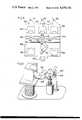
- FIG. 10shows a schematic diagram of one embodiment of sputter module 350.
- Sputter module 350includes pre-process vacuum chamber 301, wafer handler arm 340, valve 338 which provides a vacuum seal between process chamber 301 and sputter chamber 302, sputter source 304, heater 315, and match box 316.
- a waferis transferred from the wafer transport arm mechanism (not shown in FIG. 10; see FIGS. 6, 7) in transfer chamber 200 to gate valve module 100tm to wafer handler arm 340 which is shown in more detail in FIGS. 11-14 and FIG. 16.
- Gate valve module 100tmis the same as gate valve module 100 shown in FIGS. 4 and 5.
- valve 100tmis closed via a control mechanism (not shown). In this manner the atmosphere in process chamber 302 is isolated from the atmosphere in transfer chamber 200. Wafer handler arm 340 then rotates the horizontal wafer W clipped thereto through 95° within process chamber 301 so that the planar surfaces of wafer W make an angle of 5° with the vertical. This rotation is shown in perspective view in FIG. 12. Wafer handler arm 340 then rotates with wafer W clipped thereto through valve opening 338 into process chamber 302 and then rotates with wafer W through 5° so that the planar surfaces of the wafer are vertical and a portion of the back surface of wafer W rests on heater 315.
- Heater 315is well known in the art and may be, for example, part no. 682530 made by Varian Associates, Inc.
- Match box 316provides an impedance transfer between the RF heating source (not shown) and the heater glow discharge. With the wafer at a selected temperature, sputter source 304 is then activated via a control mechanism (not shown in FIG. 10. Gas line 309 provides argon gas at a selected pressure to valve 310. Needle valve 311 controls the flow of argon from valve 310 to sputter chamber 302. Needle valve 312 controls the flow of argon to the cavity formed between the back surface of wafer W and heater 315.
- Switch 308is a pressure activated switch which acts as a back up safety switch to cut power to sputter source 304 and all other electrical apparatus associated with the sputter module when the pressure in chamber 302 rises above a selected level less than or equal to atmospheric pressure.
- Interlock switch 306is a safety switch which cuts power to source 304 when the access door (not shown) in FIG. 10 is opened.
- interlock switch 314is a safety switch which cuts power to heater 315 when cooling water flow fails.
- Gauges 318 and 319measure pressure in chamber 301. Roughing gauge 318 measures pressures in the range between atmospheric pressure and 10.sup. -3 torr. Ion gauge 319 measures pressure less than approximately 10 -3 torr.
- Interlock switch 317is a safety switch which cuts power to prevent opening of valve 338 when chamber 301 is at atmospheric pressure.
- a capacitance manometer gauge 320is a pressure measuring device which senses pressure in chamber 301 and may be isolated from chamber 301 by valve 313.
- the pumping mechanism used to evacuate chamber 301is well known and includes roughing pump 323 which reduces pressure in chambers 301 and 302 via valve 336 to a selected pressure, approximately 10 -2 torr; high vacuum pump 322, for example a cryopump, then further evacuates chambers 301 and 302 via valve 324 when valve 336 is closed.
- Valve 324is closed to protect pump 322 when chamber 301 is vented to atmosphere. Chambers 301 and 302 are protected by a trap (not shown) in the pumping system foreline.
- Valve 325is used to evacuate pump 322 for starting the pump.
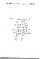
- FIG. 16shows a cross-sectional view of the mechanism by which a wafer is transferred from wafer transport arm mechanism 201 shown in FIGS. 6 and 7 to wafer arm 340 in sputter module preprocess chamber 301.
- a waferis transported into chamber 301 by arm mechanism 201 (not shown in FIG. 16, but shown in FIG. 6) being extended through port P so that wafer W carried by wafer holder 280 of arm 201 is situated above a first table 500.
- Table 500is rigidly mounted on shaft 501 which, driven by air cylinder 502, is linearly translatable vertically as indicated by double-headed arrow 518.
- Shaft 501passes through flange 397 into vacuum chamber 301.
- Bellows 522which is welded to flange 398 which is mounted to flange 397 of housing 396 and elastomeric O-ring 520 between bellows 522 and shaft 520 provide a vacuum seal between chamber 301 and the exterior atmosphere.
- Table 500is dimensioned so that it may be elevated through the circular opening in wafer holder 280 (see FIG. 6) thus removing the wafer from wafer holder 280 which is then withdrawn from chamber 301 as explained in conjunction with FIGS. 6 and 7. At this point wafer W rests on table 500 as shown in FIG. 16. Note that the edge of wafer W extends beyond the perimeter of table 500 in the scalloped areas (not shown) of table 500 where clips will eventually engage the wafer's edge.
- Wafer arm mechanism 340is rotated (as explained below) so that circular opening 342 (FIG. 11) in wafer holder plate 341 is centered above wafer W.
- a circular ceramic ring 511is mounted beneath rim 510 of wafer plate 341.
- a plurality of flexible wafer clipsare fixedly attached to ceramic ring 511 at approximately equal intervals. Two such clips, 512a and 512b, are shown in FIG. 16.
- a prong corresponding to each flexible wafer clipis rigidly attached to a second table 514. Prongs 514a and 514b corresponding to clips 512a and 512b are shown in FIG. 16.
- Table 514is rigidly attached to shaft 503 which, driven by air cylinder 504, is linearly translatable in the vertical direction as indicated by double-headed arrow 516.
- Shaft 503also passes through housing 396 of chamber 301.
- Bellows 523mounted to flange 398 of housing 396 and elastomeric O-ring 521 between bellows 523 and shaft 503 provides a vacuum seal between the chamber 301 and the exterior atmosphere.
- Arm extensions 345 and 346 of wafer plate 341are rigidly attached to shaft 365 which extends between arm extensions 345 and 346. This is shown in enlarged scale in FIG. 13.
- Shaft 365passes through gear box 360.
- Gear box 360includes a conventional right angle gear mechanism 361 for coupling the rotation of drive shaft 367 to shaft 365.
- Drive shaft 367is rotated by turning pulley 368 rigidly attached thereto and driven by a suitable mechanism, e.g., a belt attached to first motor M 1 in housing 370.
- Motor M 1drives shaft 367 which in turn, via right angle gear mechanism 361, causes wafer arm 340 on shaft 365 to rotate 95° from the horizontal (as shown in FIG. 12) along with wafer W clipped to ceramic ring 511 attached to rim 510 of wafer arm plate 341.
- Shaft 367is the inner shaft of a dual shaft coaxial feedthrough 388 (which may have ferrofluidic seals). Shaft 367 passes from vacuum chamber 301 through housing 396 to exterior pulley 368. Elastomeric O-ring 373 provides a vacuum seal between vacuum chamber 301 and the atmosphere exterior to chamber 301. Outer shaft 378 of ferrofluidic feedthrough 388, which is coaxial with inner shaft 367, also extends through housing 396 to pulley 369 which is rigidly attached thereto. Outer shaft 378 is rotated by rotating pulley 369 by a suitable means, e.g., a belt, attached to motor M 2 in housing 370.
- a suitable meanse.g., a belt
- Elastomeric O-ring 372 between ferrofluidic housing 374 and outer shaft 378provides vacuum seal between chamber 301 and the atmosphere exterior to chamber 301.
- Housing 374is welded to flange 375.
- Flange 396ais bolted to flange 375.
- Flange 396ais welded to chamber wall 396.
- O-ring 371provides a vacuum seal between chamber 301 (via flange 396a) and feedthrough 388.
- wafer arm 340When wafer arm 340 has been rotated through approximately 95° from the horizontal, as shown in FIG. 12, it is then rotated through rectangular opening 338 into sputter chamber 302. This rotation is accomplished by rotating outer shaft 378 by means of motor M 2 . The end of shaft 378 interior to chamber 301 is rigidly attached to gear box housing 360. As shaft 378 is rotated in a counterclockwise direction, gear box 360, shaft 365 and wafer arm 340 all rotate in a counterclockwise direction as shown in FIG. 12. A rotation through an angle of approximately 90° places wafer W in front of heater 315.
- wafer W attached to ceramic ring 511which is attached to wafer arm plate 341, is rotated through an angle of approximately 5° so that its back surface comes in contact with heater 315.
- a pin (not shown) adjacent heater 315engages the alignment aperture 344a in protusion 344 from wafer holder plate 341 shown in FIG. 11.
- Wafer holder plate 341may be one removable plate/shield or two stainless steel layers 341a and 341b as shown in cross section in FIG. 15.
- Top layer 341ais removably attached to bottom layer 341b by two screws (not shown).
- Top layer 341ashields bottom layer 341b from sputter deposition and helps reduce sputter deposition build up on the edge shield 530 surrounding ceramic ring 511.
- Layer 341ais replaced whenever sputter depositions on layer 341a builds up to undesirable levels.
- Sputter source 304is well known in the art; for example, sputter source 304 may be Varian CONMAGTM and is therefore not described further herein. Sputter source 304 pivots open on hinge 304a (FIG. 11) to allow access to source targets and shields.
- preprocess chamber 301When wafer handler are 340 is in preprocess chamber 301, preprocess chamber 301 may be vacuum isolated from sputter chamber 302 by means of rectangular door 351. Rectangular door 351 is attached to shaft 391 by brace 353. Shaft 391 is rotated by actuator 380 through a crank arm so that door 351 is in front of and slightly displaced from rectangular opening 338 to sputter chamber 302. As shown in FIG. 15, door 351 is dimensioned to be larger than opening 338. Door 351 is slideable with shaft 391 and is linearly translated so that O-ring 352 sealingly engages the chamber housing surrounding opening 338.
- shaft 355is translated along axis C so that end 355a engages door 351 and translates door 351 along axis C toward opening 338.
- the mechanism for driving shaft 355 contained in housing 381is shown in more detail in FIG. 14.
- Shaft 355is translated in either direction along axis C by a conventional air-driven piston attached to shaft 355.
- O-ring 383provides a dynamic vacuum seal between chamber 301 and atmosphere.
- annular extension 355b of shaft 355engages elastomeric O-ring 385 so that a static vacuum seal is formed between housing 381 and annular extension 355b.
- This novel static sealprovides more reliable vacuum isolation between chamber 301 and atmosphere.
- the modular wafer transport and processing system of the present inventionhas been described primarily with respect to its application to semiconductor wafer or substrate processing, it should be understood that the inventive system is equally useful in the processing of many other wafer or disc-like workpieces. Neither is it required that other such workpieces have flats on their edges; workpieces which are fully circular in outline can be handled as well. More specifically, the inventive system is especially useful for processing any magnetic or optical storage medium in a wafer-like or disc-like form.
Landscapes
- Engineering & Computer Science (AREA)
- Chemical & Material Sciences (AREA)
- Microelectronics & Electronic Packaging (AREA)
- General Physics & Mathematics (AREA)
- Manufacturing & Machinery (AREA)
- Computer Hardware Design (AREA)
- Physics & Mathematics (AREA)
- Power Engineering (AREA)
- Condensed Matter Physics & Semiconductors (AREA)
- Chemical Kinetics & Catalysis (AREA)
- Materials Engineering (AREA)
- Mechanical Engineering (AREA)
- Metallurgy (AREA)
- Organic Chemistry (AREA)
- Container, Conveyance, Adherence, Positioning, Of Wafer (AREA)
Abstract
Description
phi=90°-θ+cos.sup.-1 [(d/f) sin θ]
TABLE I ______________________________________ ##STR1## RA- X Y THETA PHI DIFF TIO STROKE ______________________________________ 10.00 0.00 0.00 180.00 24.00 9.99 0.52 3.00 174.86 5.14 1.71 23.98 9.95 1.05 6.00 169.72 5.14 1.71 23.91 9.88 1.56 9.00 164.58 5.13 1.71 23.79 9.78 2.08 12.00 159.46 5.12 1.71 23.63 9.66 2.59 15.00 154.35 5.11 1.70 23.42 9.51 3.09 18.00 149.25 5.10 1.70 23.17 9.34 3.58 21.00 144.17 5.08 1.69 22.87 9.14 4.07 24.00 139.11 5.06 1.69 22.53 8.91 4.54 27.00 134.08 5.03 1.68 22.15 8.66 5.00 30.00 129.08 5.00 1.67 21.74 8.39 5.45 33.00 124.11 4.97 1.66 21.28 8.09 5.88 35.00 119.17 4.93 1.64 20.80 7.77 6.29 39.00 114.29 4.89 1.63 20.28 7.43 6.69 42.00 109.45 4.84 1.61 19.73 7.07 7.07 45.00 104.66 4.78 1.59 19.15 6.69 7.43 48.00 99.94 4.72 1.57 18.56 6.29 7.77 51.00 95.28 4.66 1.55 17.94 5.88 8.09 54.00 90.70 4.58 1.53 17.30 5.45 8.39 57.00 86.21 4.49 1.50 16.66 5.00 8.66 60.00 81.80 4.41 1.47 16.00 4.54 8.91 63.00 77.49 4.31 1.44 15.34 4.07 9.14 66.00 73.28 4.21 1.40 14.68 3.58 9.34 69.00 69.19 4.09 1.36 14.02 3.09 9.51 72.00 65.22 3.97 1.32 13.37 2.59 9.66 75.00 61.39 3.84 1.28 12.72 2.08 9.78 78.00 57.69 3.70 1.23 12.10 1.57 9.88 81.00 54.14 3.55 1.18 11.49 1.05 9.95 84.00 50.75 3.40 1.13 10.90 0.52 9.99 87.00 47.51 3.24 1.08 10.34 0.00 10.00 90.00 44.43 3.08 1.03 9.80 -0.52 9.99 93.00 41.50 2.92 0.97 9.29 -1.04 9.95 96.00 38.74 2.76 0.92 8.81 -1.56 9.88 99.00 36.14 2.60 0.87 8.36 -2.08 9.78 102.00 33.69 2.45 0.82 7.94 -2.59 9.66 105.00 31.38 2.31 0.77 7.55 -3.09 9.51 108.00 29.22 2.17 0.72 7.18 -3.58 9.34 111.00 27.18 2.03 0.68 6.85 -4.07 9.14 114.00 25.27 1.91 0.64 6.54 -4.54 8.91 117.00 23.48 1.79 0.60 6.26 -5.00 8.66 120.00 21.79 1.69 0.56 6.00 -5.45 8.39 123.00 20.20 1.59 0.53 5.76 -5.88 8.09 126.00 18.71 1.50 0.50 5.55 -6.29 7.77 129.00 17.29 1.42 0.47 5.35 -6.69 7.43 132.00 15.94 1.34 0.45 5.17 -7.07 7.07 135.00 14.67 1.28 0.43 5.01 -7.43 6.69 138.00 13.45 1.22 0.41 4.87 -7.77 6.29 141.00 12.29 1.16 0.39 4.73 -8.09 5.88 144.00 11.18 1.11 0.37 4.62 -8.39 5.45 147.00 10.11 1.07 0.36 4.51 -8.66 5.00 150.00 9.08 1.03 0.34 4.42 -8.91 4.54 153.00 8.08 1.00 0.33 4.33 -9.13 4.07 156.00 7.11 0.97 0.32 4.26 -9.34 3.59 159.00 6.17 0.94 0.31 4.20 -9.51 3.09 162.00 5.25 0.92 0.31 4.14 -9.66 2.59 165.00 4.35 0.90 0.30 4.10 -9.78 2.08 168.00 3.46 0.89 0.30 4.06 -9.88 1.57 171.00 2.59 0.88 0.29 4.04 -9.94 1.05 174.00 1.72 0.87 0.29 4.02 -9.99 0.53 177.00 0.66 0.86 0.29 4.00 -10.00 0.00 180.00 0.00 0.86 0.29 4.00 ______________________________________
Claims (11)
Priority Applications (2)
| Application Number | Priority Date | Filing Date | Title |
|---|---|---|---|
| US06/856,750US4670126A (en) | 1986-04-28 | 1986-04-28 | Sputter module for modular wafer processing system |
| US07/596,119US5096364A (en) | 1986-04-28 | 1990-10-11 | Wafer arm handler mechanism |
Applications Claiming Priority (1)
| Application Number | Priority Date | Filing Date | Title |
|---|---|---|---|
| US06/856,750US4670126A (en) | 1986-04-28 | 1986-04-28 | Sputter module for modular wafer processing system |
Related Child Applications (1)
| Application Number | Title | Priority Date | Filing Date |
|---|---|---|---|
| US07053224Continuation | 1987-05-22 |
Publications (1)
| Publication Number | Publication Date |
|---|---|
| US4670126Atrue US4670126A (en) | 1987-06-02 |
Family
ID=25324416
Family Applications (1)
| Application Number | Title | Priority Date | Filing Date |
|---|---|---|---|
| US06/856,750Expired - Fee RelatedUS4670126A (en) | 1986-04-28 | 1986-04-28 | Sputter module for modular wafer processing system |
Country Status (1)
| Country | Link |
|---|---|
| US (1) | US4670126A (en) |
Cited By (379)
| Publication number | Priority date | Publication date | Assignee | Title |
|---|---|---|---|---|
| WO1989003493A1 (en)* | 1987-10-15 | 1989-04-20 | Epsilon Technology, Inc. | Chemical vapor deposition system |
| WO1989004054A1 (en)* | 1987-10-20 | 1989-05-05 | Convac Gmbh | System for manufacturing semiconductor substrates |
| US4836905A (en)* | 1987-07-16 | 1989-06-06 | Texas Instruments Incorporated | Processing apparatus |
| US4851101A (en)* | 1987-09-18 | 1989-07-25 | Varian Associates, Inc. | Sputter module for modular wafer processing machine |
| US4853102A (en)* | 1987-01-07 | 1989-08-01 | Hitachi, Ltd. | Sputtering process and an apparatus for carrying out the same |
| US4911810A (en)* | 1988-06-21 | 1990-03-27 | Brown University | Modular sputtering apparatus |
| US4923584A (en)* | 1988-10-31 | 1990-05-08 | Eaton Corporation | Sealing apparatus for a vacuum processing system |
| EP0370188A1 (en)* | 1988-11-17 | 1990-05-30 | Balzers Aktiengesellschaft | Transport device and vacuum chamber with such a device and process for loading and unloading a processing chamber |
| US4943363A (en)* | 1989-04-14 | 1990-07-24 | Leybold Aktiengesellschaft | Cathode sputtering system |
| WO1990010949A1 (en)* | 1989-03-06 | 1990-09-20 | Asm International N.V. | Method for depositing a layer on a substrate and also a processing system for that purpose |
| WO1991004213A1 (en)* | 1989-09-12 | 1991-04-04 | Rapro Technology, Inc. | Automated wafer transport system |
| US5013385A (en)* | 1986-04-18 | 1991-05-07 | General Signal Corporation | Quad processor |
| US5019233A (en)* | 1988-10-31 | 1991-05-28 | Eaton Corporation | Sputtering system |
| US5076205A (en)* | 1989-01-06 | 1991-12-31 | General Signal Corporation | Modular vapor processor system |
| US5102495A (en)* | 1986-04-18 | 1992-04-07 | General Signal Corporation | Method providing multiple-processing of substrates |
| US5154730A (en)* | 1991-05-17 | 1992-10-13 | Materials Research Corporation | Semiconductor wafer processing module having an inclined rotating wafer handling turret and a method of using the module |
| EP0526245A1 (en)* | 1991-07-31 | 1993-02-03 | Shin-Etsu Handotai Company Limited | An automatic cleaning apparatus for wafers |
| US5248371A (en)* | 1992-08-13 | 1993-09-28 | General Signal Corporation | Hollow-anode glow discharge apparatus |
| US5259942A (en)* | 1989-03-30 | 1993-11-09 | Leybold Aktiengesellschaft | Device for transferring a workpiece into and out from a vacuum chamber |
| US5295777A (en)* | 1992-12-23 | 1994-03-22 | Materials Research Corporation | Wafer transport module with rotatable and horizontally extendable wafer holder |
| US5308431A (en)* | 1986-04-18 | 1994-05-03 | General Signal Corporation | System providing multiple processing of substrates |
| US5344542A (en)* | 1986-04-18 | 1994-09-06 | General Signal Corporation | Multiple-processing and contamination-free plasma etching system |
| US5435682A (en)* | 1987-10-15 | 1995-07-25 | Advanced Semiconductor Materials America, Inc. | Chemical vapor desposition system |
| US5508519A (en)* | 1994-06-15 | 1996-04-16 | Texas Instruments Incorporated | Mainshaft shield |
| US5549435A (en)* | 1992-10-06 | 1996-08-27 | Balzers Aktiengesellschaft | Chamber and a chamber combination for a vacuum facility and a method for transporting through at least one workpiece |
| US5766360A (en)* | 1992-03-27 | 1998-06-16 | Kabushiki Kaisha Toshiba | Substrate processing apparatus and substrate processing method |
| US5791895A (en)* | 1994-02-17 | 1998-08-11 | Novellus Systems, Inc. | Apparatus for thermal treatment of thin film wafer |
| US5902407A (en)* | 1987-03-31 | 1999-05-11 | Deboer; Wiebe B. | Rotatable substrate supporting mechanism with temperature sensing device for use in chemical vapor deposition equipment |
| WO2000002808A1 (en)* | 1998-07-11 | 2000-01-20 | Semitool, Inc. | Robots for microelectronic workpiece handling |
| US6103055A (en)* | 1986-04-18 | 2000-08-15 | Applied Materials, Inc. | System for processing substrates |
| US6264804B1 (en) | 2000-04-12 | 2001-07-24 | Ske Technology Corp. | System and method for handling and masking a substrate in a sputter deposition system |
| US6318951B1 (en) | 1999-07-09 | 2001-11-20 | Semitool, Inc. | Robots for microelectronic workpiece handling |
| US6322119B1 (en) | 1999-07-09 | 2001-11-27 | Semitool, Inc. | Robots for microelectronic workpiece handling |
| US20020046707A1 (en)* | 2000-07-26 | 2002-04-25 | Biberger Maximilian A. | High pressure processing chamber for semiconductor substrate |
| US20020053509A1 (en)* | 1996-07-15 | 2002-05-09 | Hanson Kyle M. | Processing tools, components of processing tools, and method of making and using same for electrochemical processing of microelectronic workpieces |
| US6413381B1 (en) | 2000-04-12 | 2002-07-02 | Steag Hamatech Ag | Horizontal sputtering system |
| US20020125141A1 (en)* | 1999-04-13 | 2002-09-12 | Wilson Gregory J. | Tuning electrodes used in a reactor for electrochemically processing a microelectronic workpiece |
| US20020189543A1 (en)* | 2001-04-10 | 2002-12-19 | Biberger Maximilian A. | High pressure processing chamber for semiconductor substrate including flow enhancing features |
| US6537916B2 (en) | 1998-09-28 | 2003-03-25 | Tokyo Electron Limited | Removal of CMP residue from semiconductor substrate using supercritical carbon dioxide process |
| US20030062258A1 (en)* | 1998-07-10 | 2003-04-03 | Woodruff Daniel J. | Electroplating apparatus with segmented anode array |
| US20030082042A1 (en)* | 2001-07-13 | 2003-05-01 | Woodruff Daniel J. | End-effectors for handling microelectronic workpieces |
| US20030085582A1 (en)* | 2001-07-13 | 2003-05-08 | Woodruff Daniel J. | End-effectors for handling microelectronic workpieces |
| US20030121535A1 (en)* | 1999-11-02 | 2003-07-03 | Biberger Maximilian Albert | Method for supercritical processing of multiple workpieces |
| US20030150559A1 (en)* | 1999-11-02 | 2003-08-14 | Biberger Maximilian Albert | Apparatus for supercritical processing of a workpiece |
| US20030155541A1 (en)* | 2002-02-15 | 2003-08-21 | Supercritical Systems, Inc. | Pressure enhanced diaphragm valve |
| US20030159921A1 (en)* | 2002-02-22 | 2003-08-28 | Randy Harris | Apparatus with processing stations for manually and automatically processing microelectronic workpieces |
| US20030159277A1 (en)* | 2002-02-22 | 2003-08-28 | Randy Harris | Method and apparatus for manually and automatically processing microelectronic workpieces |
| US6650409B1 (en)* | 1991-04-02 | 2003-11-18 | Hitachi, Ltd. | Semiconductor device producing method, system for carrying out the same and semiconductor work processing apparatus included in the same system |
| US6656330B2 (en)* | 2000-06-22 | 2003-12-02 | Unaxis Balzers Aktiengesellschaft | Coating installation for disk-form workpieces |
| US20040040660A1 (en)* | 2001-10-03 | 2004-03-04 | Biberger Maximilian Albert | High pressure processing chamber for multiple semiconductor substrates |
| US20040094086A1 (en)* | 2001-03-29 | 2004-05-20 | Keiichi Shimaoka | Production device and production method for silicon-based structure |
| US6749391B2 (en) | 1996-07-15 | 2004-06-15 | Semitool, Inc. | Microelectronic workpiece transfer devices and methods of using such devices in the processing of microelectronic workpieces |
| US6749390B2 (en) | 1997-12-15 | 2004-06-15 | Semitool, Inc. | Integrated tools with transfer devices for handling microelectronic workpieces |
| US20040112409A1 (en)* | 2002-12-16 | 2004-06-17 | Supercritical Sysems, Inc. | Fluoride in supercritical fluid for photoresist and residue removal |
| US6752584B2 (en) | 1996-07-15 | 2004-06-22 | Semitool, Inc. | Transfer devices for handling microelectronic workpieces within an environment of a processing machine and methods of manufacturing and using such devices in the processing of microelectronic workpieces |
| US20040118005A1 (en)* | 1995-07-19 | 2004-06-24 | Minoru Soraoka | Vacuum processing apparatus and semiconductor manufacturing line using the same |
| US20040157420A1 (en)* | 2003-02-06 | 2004-08-12 | Supercritical Systems, Inc. | Vacuum chuck utilizing sintered material and method of providing thereof |
| US20040154647A1 (en)* | 2003-02-07 | 2004-08-12 | Supercritical Systems, Inc. | Method and apparatus of utilizing a coating for enhanced holding of a semiconductor substrate during high pressure processing |
| US20040157463A1 (en)* | 2003-02-10 | 2004-08-12 | Supercritical Systems, Inc. | High-pressure processing chamber for a semiconductor wafer |
| US20040187337A1 (en)* | 1990-08-29 | 2004-09-30 | Shigekazu Kato | Vacuum processing apparatus and operating method therefor |
| US20040229449A1 (en)* | 2000-04-25 | 2004-11-18 | Biberger Maximilian A. | Method of depositing metal film and metal deposition cluster tool including supercritical drying/cleaning module |
| US20050014370A1 (en)* | 2003-02-10 | 2005-01-20 | Supercritical Systems, Inc. | High-pressure processing chamber for a semiconductor wafer |
| US20050025628A1 (en)* | 2003-07-29 | 2005-02-03 | Supercritical Systems, Inc. | Control of fluid flow in the processing of an object with a fluid |
| US20050034660A1 (en)* | 2003-08-11 | 2005-02-17 | Supercritical Systems, Inc. | Alignment means for chamber closure to reduce wear on surfaces |
| US20050035514A1 (en)* | 2003-08-11 | 2005-02-17 | Supercritical Systems, Inc. | Vacuum chuck apparatus and method for holding a wafer during high pressure processing |
| US6871656B2 (en) | 1997-05-27 | 2005-03-29 | Tokyo Electron Limited | Removal of photoresist and photoresist residue from semiconductors using supercritical carbon dioxide process |
| US20050067002A1 (en)* | 2003-09-25 | 2005-03-31 | Supercritical Systems, Inc. | Processing chamber including a circulation loop integrally formed in a chamber housing |
| US6916412B2 (en) | 1999-04-13 | 2005-07-12 | Semitool, Inc. | Adaptable electrochemical processing chamber |
| US20050191865A1 (en)* | 2002-03-04 | 2005-09-01 | Gunilla Jacobson | Treatment of a dielectric layer using supercritical CO2 |
| US6976822B2 (en) | 2002-07-16 | 2005-12-20 | Semitool, Inc. | End-effectors and transfer devices for handling microelectronic workpieces |
| US7001468B1 (en) | 2002-02-15 | 2006-02-21 | Tokyo Electron Limited | Pressure energized pressure vessel opening and closing device and method of providing therefor |
| US20060043750A1 (en)* | 2004-07-09 | 2006-03-02 | Paul Wirth | End-effectors for handling microfeature workpieces |
| US20060054495A1 (en)* | 2004-09-10 | 2006-03-16 | Hartmut Rohrmann | Substrate processing system |
| US7020537B2 (en) | 1999-04-13 | 2006-03-28 | Semitool, Inc. | Tuning electrodes used in a reactor for electrochemically processing a microelectronic workpiece |
| US20060065288A1 (en)* | 2004-09-30 | 2006-03-30 | Darko Babic | Supercritical fluid processing system having a coating on internal members and a method of using |
| US20060065189A1 (en)* | 2004-09-30 | 2006-03-30 | Darko Babic | Method and system for homogenization of supercritical fluid in a high pressure processing system |
| US20060073041A1 (en)* | 2004-10-05 | 2006-04-06 | Supercritical Systems Inc. | Temperature controlled high pressure pump |
| US20060130913A1 (en)* | 2004-12-22 | 2006-06-22 | Alexei Sheydayi | Non-contact shuttle valve for flow diversion in high pressure systems |
| US20060135047A1 (en)* | 2004-12-22 | 2006-06-22 | Alexei Sheydayi | Method and apparatus for clamping a substrate in a high pressure processing system |
| US20060134332A1 (en)* | 2004-12-22 | 2006-06-22 | Darko Babic | Precompressed coating of internal members in a supercritical fluid processing system |
| US20060130875A1 (en)* | 2004-12-22 | 2006-06-22 | Alexei Sheydayi | Method and apparatus for clamping a substrate in a high pressure processing system |
| US7090751B2 (en) | 2001-08-31 | 2006-08-15 | Semitool, Inc. | Apparatus and methods for electrochemical processing of microelectronic workpieces |
| US20060180175A1 (en)* | 2005-02-15 | 2006-08-17 | Parent Wayne M | Method and system for determining flow conditions in a high pressure processing system |
| US20060216197A1 (en)* | 2005-03-28 | 2006-09-28 | Jones William D | High pressure fourier transform infrared cell |
| US20060215729A1 (en)* | 2005-03-28 | 2006-09-28 | Wuester Christopher D | Process flow thermocouple |
| US7115196B2 (en) | 1998-03-20 | 2006-10-03 | Semitool, Inc. | Apparatus and method for electrochemically depositing metal on a semiconductor workpiece |
| US20060225772A1 (en)* | 2005-03-29 | 2006-10-12 | Jones William D | Controlled pressure differential in a high-pressure processing chamber |
| US20060225811A1 (en)* | 2005-03-30 | 2006-10-12 | Alexei Sheydayi | Gate valve for plus-atmospheric pressure semiconductor process vessels |
| US20060266287A1 (en)* | 2005-05-25 | 2006-11-30 | Parent Wayne M | Method and system for passivating a processing chamber |
| US20070014656A1 (en)* | 2002-07-11 | 2007-01-18 | Harris Randy A | End-effectors and associated control and guidance systems and methods |
| US20070020080A1 (en)* | 2004-07-09 | 2007-01-25 | Paul Wirth | Transfer devices and methods for handling microfeature workpieces within an environment of a processing machine |
| US7189318B2 (en) | 1999-04-13 | 2007-03-13 | Semitool, Inc. | Tuning electrodes used in a reactor for electrochemically processing a microelectronic workpiece |
| US7250374B2 (en) | 2004-06-30 | 2007-07-31 | Tokyo Electron Limited | System and method for processing a substrate using supercritical carbon dioxide processing |
| US7264698B2 (en) | 1999-04-13 | 2007-09-04 | Semitool, Inc. | Apparatus and methods for electrochemical processing of microelectronic workpieces |
| US7267749B2 (en) | 1999-04-13 | 2007-09-11 | Semitool, Inc. | Workpiece processor having processing chamber with improved processing fluid flow |
| US7270137B2 (en) | 2003-04-28 | 2007-09-18 | Tokyo Electron Limited | Apparatus and method of securing a workpiece during high-pressure processing |
| US7291565B2 (en) | 2005-02-15 | 2007-11-06 | Tokyo Electron Limited | Method and system for treating a substrate with a high pressure fluid using fluorosilicic acid |
| US7307019B2 (en) | 2004-09-29 | 2007-12-11 | Tokyo Electron Limited | Method for supercritical carbon dioxide processing of fluoro-carbon films |
| US7351315B2 (en) | 2003-12-05 | 2008-04-01 | Semitool, Inc. | Chambers, systems, and methods for electrochemically processing microfeature workpieces |
| US7351314B2 (en) | 2003-12-05 | 2008-04-01 | Semitool, Inc. | Chambers, systems, and methods for electrochemically processing microfeature workpieces |
| US7438788B2 (en) | 1999-04-13 | 2008-10-21 | Semitool, Inc. | Apparatus and methods for electrochemical processing of microelectronic workpieces |
| US7491036B2 (en) | 2004-11-12 | 2009-02-17 | Tokyo Electron Limited | Method and system for cooling a pump |
| US7585398B2 (en) | 1999-04-13 | 2009-09-08 | Semitool, Inc. | Chambers, systems, and methods for electrochemically processing microfeature workpieces |
| US7789971B2 (en) | 2005-05-13 | 2010-09-07 | Tokyo Electron Limited | Treatment of substrate using functionalizing agent in supercritical carbon dioxide |
| US20130019797A1 (en)* | 2011-07-14 | 2013-01-24 | Sen Corporation | Impurity-doped layer formation apparatus and electrostatic chuck protection method |
| US11001925B2 (en) | 2016-12-19 | 2021-05-11 | Asm Ip Holding B.V. | Substrate processing apparatus |
| US11004977B2 (en) | 2017-07-19 | 2021-05-11 | Asm Ip Holding B.V. | Method for depositing a group IV semiconductor and related semiconductor device structures |
| US11015245B2 (en) | 2014-03-19 | 2021-05-25 | Asm Ip Holding B.V. | Gas-phase reactor and system having exhaust plenum and components thereof |
| US11018002B2 (en) | 2017-07-19 | 2021-05-25 | Asm Ip Holding B.V. | Method for selectively depositing a Group IV semiconductor and related semiconductor device structures |
| US11022879B2 (en) | 2017-11-24 | 2021-06-01 | Asm Ip Holding B.V. | Method of forming an enhanced unexposed photoresist layer |
| US11031242B2 (en) | 2018-11-07 | 2021-06-08 | Asm Ip Holding B.V. | Methods for depositing a boron doped silicon germanium film |
| USD922229S1 (en) | 2019-06-05 | 2021-06-15 | Asm Ip Holding B.V. | Device for controlling a temperature of a gas supply unit |
| US11049751B2 (en) | 2018-09-14 | 2021-06-29 | Asm Ip Holding B.V. | Cassette supply system to store and handle cassettes and processing apparatus equipped therewith |
| US11056344B2 (en) | 2017-08-30 | 2021-07-06 | Asm Ip Holding B.V. | Layer forming method |
| US11053591B2 (en) | 2018-08-06 | 2021-07-06 | Asm Ip Holding B.V. | Multi-port gas injection system and reactor system including same |
| US11069510B2 (en) | 2017-08-30 | 2021-07-20 | Asm Ip Holding B.V. | Substrate processing apparatus |
| US11081345B2 (en) | 2018-02-06 | 2021-08-03 | Asm Ip Holding B.V. | Method of post-deposition treatment for silicon oxide film |
| US11087997B2 (en) | 2018-10-31 | 2021-08-10 | Asm Ip Holding B.V. | Substrate processing apparatus for processing substrates |
| US11088002B2 (en) | 2018-03-29 | 2021-08-10 | Asm Ip Holding B.V. | Substrate rack and a substrate processing system and method |
| US11094546B2 (en) | 2017-10-05 | 2021-08-17 | Asm Ip Holding B.V. | Method for selectively depositing a metallic film on a substrate |
| US11094582B2 (en) | 2016-07-08 | 2021-08-17 | Asm Ip Holding B.V. | Selective deposition method to form air gaps |
| US11101370B2 (en) | 2016-05-02 | 2021-08-24 | Asm Ip Holding B.V. | Method of forming a germanium oxynitride film |
| US11107676B2 (en) | 2016-07-28 | 2021-08-31 | Asm Ip Holding B.V. | Method and apparatus for filling a gap |
| US11114294B2 (en) | 2019-03-08 | 2021-09-07 | Asm Ip Holding B.V. | Structure including SiOC layer and method of forming same |
| US11114283B2 (en) | 2018-03-16 | 2021-09-07 | Asm Ip Holding B.V. | Reactor, system including the reactor, and methods of manufacturing and using same |
| USD930782S1 (en) | 2019-08-22 | 2021-09-14 | Asm Ip Holding B.V. | Gas distributor |
| US11127589B2 (en) | 2019-02-01 | 2021-09-21 | Asm Ip Holding B.V. | Method of topology-selective film formation of silicon oxide |
| US11127617B2 (en) | 2017-11-27 | 2021-09-21 | Asm Ip Holding B.V. | Storage device for storing wafer cassettes for use with a batch furnace |
| USD931978S1 (en) | 2019-06-27 | 2021-09-28 | Asm Ip Holding B.V. | Showerhead vacuum transport |
| US11139308B2 (en) | 2015-12-29 | 2021-10-05 | Asm Ip Holding B.V. | Atomic layer deposition of III-V compounds to form V-NAND devices |
| US11139191B2 (en) | 2017-08-09 | 2021-10-05 | Asm Ip Holding B.V. | Storage apparatus for storing cassettes for substrates and processing apparatus equipped therewith |
| US11158513B2 (en) | 2018-12-13 | 2021-10-26 | Asm Ip Holding B.V. | Methods for forming a rhenium-containing film on a substrate by a cyclical deposition process and related semiconductor device structures |
| US11164955B2 (en) | 2017-07-18 | 2021-11-02 | Asm Ip Holding B.V. | Methods for forming a semiconductor device structure and related semiconductor device structures |
| US11171025B2 (en) | 2019-01-22 | 2021-11-09 | Asm Ip Holding B.V. | Substrate processing device |
| US11168395B2 (en) | 2018-06-29 | 2021-11-09 | Asm Ip Holding B.V. | Temperature-controlled flange and reactor system including same |
| USD935572S1 (en) | 2019-05-24 | 2021-11-09 | Asm Ip Holding B.V. | Gas channel plate |
| US11205585B2 (en) | 2016-07-28 | 2021-12-21 | Asm Ip Holding B.V. | Substrate processing apparatus and method of operating the same |
| US11217444B2 (en) | 2018-11-30 | 2022-01-04 | Asm Ip Holding B.V. | Method for forming an ultraviolet radiation responsive metal oxide-containing film |
| US11222772B2 (en) | 2016-12-14 | 2022-01-11 | Asm Ip Holding B.V. | Substrate processing apparatus |
| USD940837S1 (en) | 2019-08-22 | 2022-01-11 | Asm Ip Holding B.V. | Electrode |
| US11227782B2 (en) | 2019-07-31 | 2022-01-18 | Asm Ip Holding B.V. | Vertical batch furnace assembly |
| US11227789B2 (en) | 2019-02-20 | 2022-01-18 | Asm Ip Holding B.V. | Method and apparatus for filling a recess formed within a substrate surface |
| US11233133B2 (en) | 2015-10-21 | 2022-01-25 | Asm Ip Holding B.V. | NbMC layers |
| US11230766B2 (en) | 2018-03-29 | 2022-01-25 | Asm Ip Holding B.V. | Substrate processing apparatus and method |
| US11232963B2 (en) | 2018-10-03 | 2022-01-25 | Asm Ip Holding B.V. | Substrate processing apparatus and method |
| US11242598B2 (en) | 2015-06-26 | 2022-02-08 | Asm Ip Holding B.V. | Structures including metal carbide material, devices including the structures, and methods of forming same |
| US11244825B2 (en) | 2018-11-16 | 2022-02-08 | Asm Ip Holding B.V. | Methods for depositing a transition metal chalcogenide film on a substrate by a cyclical deposition process |
| US11251040B2 (en) | 2019-02-20 | 2022-02-15 | Asm Ip Holding B.V. | Cyclical deposition method including treatment step and apparatus for same |
| US11251035B2 (en) | 2016-12-22 | 2022-02-15 | Asm Ip Holding B.V. | Method of forming a structure on a substrate |
| US11251068B2 (en) | 2018-10-19 | 2022-02-15 | Asm Ip Holding B.V. | Substrate processing apparatus and substrate processing method |
| USD944946S1 (en) | 2019-06-14 | 2022-03-01 | Asm Ip Holding B.V. | Shower plate |
| US11270899B2 (en) | 2018-06-04 | 2022-03-08 | Asm Ip Holding B.V. | Wafer handling chamber with moisture reduction |
| US11274369B2 (en) | 2018-09-11 | 2022-03-15 | Asm Ip Holding B.V. | Thin film deposition method |
| US11282698B2 (en) | 2019-07-19 | 2022-03-22 | Asm Ip Holding B.V. | Method of forming topology-controlled amorphous carbon polymer film |
| US11289326B2 (en) | 2019-05-07 | 2022-03-29 | Asm Ip Holding B.V. | Method for reforming amorphous carbon polymer film |
| US11286558B2 (en) | 2019-08-23 | 2022-03-29 | Asm Ip Holding B.V. | Methods for depositing a molybdenum nitride film on a surface of a substrate by a cyclical deposition process and related semiconductor device structures including a molybdenum nitride film |
| US11286562B2 (en) | 2018-06-08 | 2022-03-29 | Asm Ip Holding B.V. | Gas-phase chemical reactor and method of using same |
| USD947913S1 (en) | 2019-05-17 | 2022-04-05 | Asm Ip Holding B.V. | Susceptor shaft |
| US11296189B2 (en) | 2018-06-21 | 2022-04-05 | Asm Ip Holding B.V. | Method for depositing a phosphorus doped silicon arsenide film and related semiconductor device structures |
| US11295980B2 (en) | 2017-08-30 | 2022-04-05 | Asm Ip Holding B.V. | Methods for depositing a molybdenum metal film over a dielectric surface of a substrate by a cyclical deposition process and related semiconductor device structures |
| USD948463S1 (en) | 2018-10-24 | 2022-04-12 | Asm Ip Holding B.V. | Susceptor for semiconductor substrate supporting apparatus |
| USD949319S1 (en) | 2019-08-22 | 2022-04-19 | Asm Ip Holding B.V. | Exhaust duct |
| US11306395B2 (en) | 2017-06-28 | 2022-04-19 | Asm Ip Holding B.V. | Methods for depositing a transition metal nitride film on a substrate by atomic layer deposition and related deposition apparatus |
| US11315794B2 (en) | 2019-10-21 | 2022-04-26 | Asm Ip Holding B.V. | Apparatus and methods for selectively etching films |
| US11339476B2 (en) | 2019-10-08 | 2022-05-24 | Asm Ip Holding B.V. | Substrate processing device having connection plates, substrate processing method |
| US11342216B2 (en) | 2019-02-20 | 2022-05-24 | Asm Ip Holding B.V. | Cyclical deposition method and apparatus for filling a recess formed within a substrate surface |
| US11345999B2 (en) | 2019-06-06 | 2022-05-31 | Asm Ip Holding B.V. | Method of using a gas-phase reactor system including analyzing exhausted gas |
| US11355338B2 (en) | 2019-05-10 | 2022-06-07 | Asm Ip Holding B.V. | Method of depositing material onto a surface and structure formed according to the method |
| US11361990B2 (en) | 2018-05-28 | 2022-06-14 | Asm Ip Holding B.V. | Substrate processing method and device manufactured by using the same |
| US11374112B2 (en) | 2017-07-19 | 2022-06-28 | Asm Ip Holding B.V. | Method for depositing a group IV semiconductor and related semiconductor device structures |
| US11378337B2 (en) | 2019-03-28 | 2022-07-05 | Asm Ip Holding B.V. | Door opener and substrate processing apparatus provided therewith |
| US11387120B2 (en) | 2017-09-28 | 2022-07-12 | Asm Ip Holding B.V. | Chemical dispensing apparatus and methods for dispensing a chemical to a reaction chamber |
| US11387106B2 (en) | 2018-02-14 | 2022-07-12 | Asm Ip Holding B.V. | Method for depositing a ruthenium-containing film on a substrate by a cyclical deposition process |
| US11390945B2 (en) | 2019-07-03 | 2022-07-19 | Asm Ip Holding B.V. | Temperature control assembly for substrate processing apparatus and method of using same |
| US11393690B2 (en) | 2018-01-19 | 2022-07-19 | Asm Ip Holding B.V. | Deposition method |
| US11390950B2 (en) | 2017-01-10 | 2022-07-19 | Asm Ip Holding B.V. | Reactor system and method to reduce residue buildup during a film deposition process |
| US11390946B2 (en) | 2019-01-17 | 2022-07-19 | Asm Ip Holding B.V. | Methods of forming a transition metal containing film on a substrate by a cyclical deposition process |
| US11396702B2 (en) | 2016-11-15 | 2022-07-26 | Asm Ip Holding B.V. | Gas supply unit and substrate processing apparatus including the gas supply unit |
| US11398382B2 (en) | 2018-03-27 | 2022-07-26 | Asm Ip Holding B.V. | Method of forming an electrode on a substrate and a semiconductor device structure including an electrode |
| US11401605B2 (en) | 2019-11-26 | 2022-08-02 | Asm Ip Holding B.V. | Substrate processing apparatus |
| US11411088B2 (en) | 2018-11-16 | 2022-08-09 | Asm Ip Holding B.V. | Methods for forming a metal silicate film on a substrate in a reaction chamber and related semiconductor device structures |
| US11410851B2 (en) | 2017-02-15 | 2022-08-09 | Asm Ip Holding B.V. | Methods for forming a metallic film on a substrate by cyclical deposition and related semiconductor device structures |
| US11414760B2 (en) | 2018-10-08 | 2022-08-16 | Asm Ip Holding B.V. | Substrate support unit, thin film deposition apparatus including the same, and substrate processing apparatus including the same |
| US11417545B2 (en) | 2017-08-08 | 2022-08-16 | Asm Ip Holding B.V. | Radiation shield |
| US11424119B2 (en) | 2019-03-08 | 2022-08-23 | Asm Ip Holding B.V. | Method for selective deposition of silicon nitride layer and structure including selectively-deposited silicon nitride layer |
| US11430674B2 (en) | 2018-08-22 | 2022-08-30 | Asm Ip Holding B.V. | Sensor array, apparatus for dispensing a vapor phase reactant to a reaction chamber and related methods |
| US11430640B2 (en) | 2019-07-30 | 2022-08-30 | Asm Ip Holding B.V. | Substrate processing apparatus |
| US11437241B2 (en) | 2020-04-08 | 2022-09-06 | Asm Ip Holding B.V. | Apparatus and methods for selectively etching silicon oxide films |
| US11443926B2 (en) | 2019-07-30 | 2022-09-13 | Asm Ip Holding B.V. | Substrate processing apparatus |
| US11447864B2 (en) | 2019-04-19 | 2022-09-20 | Asm Ip Holding B.V. | Layer forming method and apparatus |
| US11447861B2 (en) | 2016-12-15 | 2022-09-20 | Asm Ip Holding B.V. | Sequential infiltration synthesis apparatus and a method of forming a patterned structure |
| US11453943B2 (en) | 2016-05-25 | 2022-09-27 | Asm Ip Holding B.V. | Method for forming carbon-containing silicon/metal oxide or nitride film by ALD using silicon precursor and hydrocarbon precursor |
| USD965044S1 (en) | 2019-08-19 | 2022-09-27 | Asm Ip Holding B.V. | Susceptor shaft |
| USD965524S1 (en) | 2019-08-19 | 2022-10-04 | Asm Ip Holding B.V. | Susceptor support |
| US11469098B2 (en) | 2018-05-08 | 2022-10-11 | Asm Ip Holding B.V. | Methods for depositing an oxide film on a substrate by a cyclical deposition process and related device structures |
| US11473195B2 (en) | 2018-03-01 | 2022-10-18 | Asm Ip Holding B.V. | Semiconductor processing apparatus and a method for processing a substrate |
| US11476109B2 (en) | 2019-06-11 | 2022-10-18 | Asm Ip Holding B.V. | Method of forming an electronic structure using reforming gas, system for performing the method, and structure formed using the method |
| US11482533B2 (en) | 2019-02-20 | 2022-10-25 | Asm Ip Holding B.V. | Apparatus and methods for plug fill deposition in 3-D NAND applications |
| US11482412B2 (en) | 2018-01-19 | 2022-10-25 | Asm Ip Holding B.V. | Method for depositing a gap-fill layer by plasma-assisted deposition |
| US11482418B2 (en) | 2018-02-20 | 2022-10-25 | Asm Ip Holding B.V. | Substrate processing method and apparatus |
| US11488854B2 (en) | 2020-03-11 | 2022-11-01 | Asm Ip Holding B.V. | Substrate handling device with adjustable joints |
| US11488819B2 (en) | 2018-12-04 | 2022-11-01 | Asm Ip Holding B.V. | Method of cleaning substrate processing apparatus |
| US11492703B2 (en) | 2018-06-27 | 2022-11-08 | Asm Ip Holding B.V. | Cyclic deposition methods for forming metal-containing material and films and structures including the metal-containing material |
| US11495459B2 (en) | 2019-09-04 | 2022-11-08 | Asm Ip Holding B.V. | Methods for selective deposition using a sacrificial capping layer |
| US11501968B2 (en) | 2019-11-15 | 2022-11-15 | Asm Ip Holding B.V. | Method for providing a semiconductor device with silicon filled gaps |
| US11501956B2 (en) | 2012-10-12 | 2022-11-15 | Asm Ip Holding B.V. | Semiconductor reaction chamber showerhead |
| US11501973B2 (en) | 2018-01-16 | 2022-11-15 | Asm Ip Holding B.V. | Method for depositing a material film on a substrate within a reaction chamber by a cyclical deposition process and related device structures |
| US11499222B2 (en) | 2018-06-27 | 2022-11-15 | Asm Ip Holding B.V. | Cyclic deposition methods for forming metal-containing material and films and structures including the metal-containing material |
| US11499226B2 (en) | 2018-11-02 | 2022-11-15 | Asm Ip Holding B.V. | Substrate supporting unit and a substrate processing device including the same |
| US11515187B2 (en) | 2020-05-01 | 2022-11-29 | Asm Ip Holding B.V. | Fast FOUP swapping with a FOUP handler |
| US11515188B2 (en) | 2019-05-16 | 2022-11-29 | Asm Ip Holding B.V. | Wafer boat handling device, vertical batch furnace and method |
| US11521851B2 (en) | 2020-02-03 | 2022-12-06 | Asm Ip Holding B.V. | Method of forming structures including a vanadium or indium layer |
| US11527403B2 (en) | 2019-12-19 | 2022-12-13 | Asm Ip Holding B.V. | Methods for filling a gap feature on a substrate surface and related semiconductor structures |
| US11527400B2 (en) | 2019-08-23 | 2022-12-13 | Asm Ip Holding B.V. | Method for depositing silicon oxide film having improved quality by peald using bis(diethylamino)silane |
| US11532757B2 (en) | 2016-10-27 | 2022-12-20 | Asm Ip Holding B.V. | Deposition of charge trapping layers |
| US11530483B2 (en) | 2018-06-21 | 2022-12-20 | Asm Ip Holding B.V. | Substrate processing system |
| US11530876B2 (en) | 2020-04-24 | 2022-12-20 | Asm Ip Holding B.V. | Vertical batch furnace assembly comprising a cooling gas supply |
| US11551912B2 (en) | 2020-01-20 | 2023-01-10 | Asm Ip Holding B.V. | Method of forming thin film and method of modifying surface of thin film |
| US11551925B2 (en) | 2019-04-01 | 2023-01-10 | Asm Ip Holding B.V. | Method for manufacturing a semiconductor device |
| US11557474B2 (en) | 2019-07-29 | 2023-01-17 | Asm Ip Holding B.V. | Methods for selective deposition utilizing n-type dopants and/or alternative dopants to achieve high dopant incorporation |
| USD975665S1 (en) | 2019-05-17 | 2023-01-17 | Asm Ip Holding B.V. | Susceptor shaft |
| US11562901B2 (en) | 2019-09-25 | 2023-01-24 | Asm Ip Holding B.V. | Substrate processing method |
| US11572620B2 (en) | 2018-11-06 | 2023-02-07 | Asm Ip Holding B.V. | Methods for selectively depositing an amorphous silicon film on a substrate |
| US11581186B2 (en) | 2016-12-15 | 2023-02-14 | Asm Ip Holding B.V. | Sequential infiltration synthesis apparatus |
| US11587815B2 (en) | 2019-07-31 | 2023-02-21 | Asm Ip Holding B.V. | Vertical batch furnace assembly |
| US11587821B2 (en) | 2017-08-08 | 2023-02-21 | Asm Ip Holding B.V. | Substrate lift mechanism and reactor including same |
| US11587814B2 (en) | 2019-07-31 | 2023-02-21 | Asm Ip Holding B.V. | Vertical batch furnace assembly |
| US11594450B2 (en) | 2019-08-22 | 2023-02-28 | Asm Ip Holding B.V. | Method for forming a structure with a hole |
| US11594600B2 (en) | 2019-11-05 | 2023-02-28 | Asm Ip Holding B.V. | Structures with doped semiconductor layers and methods and systems for forming same |
| USD979506S1 (en) | 2019-08-22 | 2023-02-28 | Asm Ip Holding B.V. | Insulator |
| US11605528B2 (en) | 2019-07-09 | 2023-03-14 | Asm Ip Holding B.V. | Plasma device using coaxial waveguide, and substrate treatment method |
| USD980813S1 (en) | 2021-05-11 | 2023-03-14 | Asm Ip Holding B.V. | Gas flow control plate for substrate processing apparatus |
| USD980814S1 (en) | 2021-05-11 | 2023-03-14 | Asm Ip Holding B.V. | Gas distributor for substrate processing apparatus |
| US11610775B2 (en) | 2016-07-28 | 2023-03-21 | Asm Ip Holding B.V. | Method and apparatus for filling a gap |
| US11610774B2 (en) | 2019-10-02 | 2023-03-21 | Asm Ip Holding B.V. | Methods for forming a topographically selective silicon oxide film by a cyclical plasma-enhanced deposition process |
| US11615970B2 (en) | 2019-07-17 | 2023-03-28 | Asm Ip Holding B.V. | Radical assist ignition plasma system and method |
| USD981973S1 (en) | 2021-05-11 | 2023-03-28 | Asm Ip Holding B.V. | Reactor wall for substrate processing apparatus |
| US11626316B2 (en) | 2019-11-20 | 2023-04-11 | Asm Ip Holding B.V. | Method of depositing carbon-containing material on a surface of a substrate, structure formed using the method, and system for forming the structure |
| US11626308B2 (en) | 2020-05-13 | 2023-04-11 | Asm Ip Holding B.V. | Laser alignment fixture for a reactor system |
| US11629407B2 (en) | 2019-02-22 | 2023-04-18 | Asm Ip Holding B.V. | Substrate processing apparatus and method for processing substrates |
| US11629406B2 (en) | 2018-03-09 | 2023-04-18 | Asm Ip Holding B.V. | Semiconductor processing apparatus comprising one or more pyrometers for measuring a temperature of a substrate during transfer of the substrate |
| US11637011B2 (en) | 2019-10-16 | 2023-04-25 | Asm Ip Holding B.V. | Method of topology-selective film formation of silicon oxide |
| US11637014B2 (en) | 2019-10-17 | 2023-04-25 | Asm Ip Holding B.V. | Methods for selective deposition of doped semiconductor material |
| US11639811B2 (en) | 2017-11-27 | 2023-05-02 | Asm Ip Holding B.V. | Apparatus including a clean mini environment |
| US11639548B2 (en) | 2019-08-21 | 2023-05-02 | Asm Ip Holding B.V. | Film-forming material mixed-gas forming device and film forming device |
| US11646197B2 (en) | 2018-07-03 | 2023-05-09 | Asm Ip Holding B.V. | Method for depositing silicon-free carbon-containing film as gap-fill layer by pulse plasma-assisted deposition |
| US11643724B2 (en) | 2019-07-18 | 2023-05-09 | Asm Ip Holding B.V. | Method of forming structures using a neutral beam |
| US11644758B2 (en) | 2020-07-17 | 2023-05-09 | Asm Ip Holding B.V. | Structures and methods for use in photolithography |
| US11646184B2 (en) | 2019-11-29 | 2023-05-09 | Asm Ip Holding B.V. | Substrate processing apparatus |
| US11646204B2 (en) | 2020-06-24 | 2023-05-09 | Asm Ip Holding B.V. | Method for forming a layer provided with silicon |
| US11646205B2 (en) | 2019-10-29 | 2023-05-09 | Asm Ip Holding B.V. | Methods of selectively forming n-type doped material on a surface, systems for selectively forming n-type doped material, and structures formed using same |
| US11649546B2 (en) | 2016-07-08 | 2023-05-16 | Asm Ip Holding B.V. | Organic reactants for atomic layer deposition |
| US11658030B2 (en) | 2017-03-29 | 2023-05-23 | Asm Ip Holding B.V. | Method for forming doped metal oxide films on a substrate by cyclical deposition and related semiconductor device structures |
| US11658029B2 (en) | 2018-12-14 | 2023-05-23 | Asm Ip Holding B.V. | Method of forming a device structure using selective deposition of gallium nitride and system for same |
| US11658035B2 (en) | 2020-06-30 | 2023-05-23 | Asm Ip Holding B.V. | Substrate processing method |
| US11664245B2 (en) | 2019-07-16 | 2023-05-30 | Asm Ip Holding B.V. | Substrate processing device |
| US11664267B2 (en) | 2019-07-10 | 2023-05-30 | Asm Ip Holding B.V. | Substrate support assembly and substrate processing device including the same |
| US11664199B2 (en) | 2018-10-19 | 2023-05-30 | Asm Ip Holding B.V. | Substrate processing apparatus and substrate processing method |
| US11674220B2 (en) | 2020-07-20 | 2023-06-13 | Asm Ip Holding B.V. | Method for depositing molybdenum layers using an underlayer |
| US11676812B2 (en) | 2016-02-19 | 2023-06-13 | Asm Ip Holding B.V. | Method for forming silicon nitride film selectively on top/bottom portions |
| US11680839B2 (en) | 2019-08-05 | 2023-06-20 | Asm Ip Holding B.V. | Liquid level sensor for a chemical source vessel |
| US11688603B2 (en) | 2019-07-17 | 2023-06-27 | Asm Ip Holding B.V. | Methods of forming silicon germanium structures |
| US11685991B2 (en) | 2018-02-14 | 2023-06-27 | Asm Ip Holding B.V. | Method for depositing a ruthenium-containing film on a substrate by a cyclical deposition process |
| USD990441S1 (en) | 2021-09-07 | 2023-06-27 | Asm Ip Holding B.V. | Gas flow control plate |
| USD990534S1 (en) | 2020-09-11 | 2023-06-27 | Asm Ip Holding B.V. | Weighted lift pin |
| US11705333B2 (en) | 2020-05-21 | 2023-07-18 | Asm Ip Holding B.V. | Structures including multiple carbon layers and methods of forming and using same |
| US11718913B2 (en) | 2018-06-04 | 2023-08-08 | Asm Ip Holding B.V. | Gas distribution system and reactor system including same |
| US11725280B2 (en) | 2020-08-26 | 2023-08-15 | Asm Ip Holding B.V. | Method for forming metal silicon oxide and metal silicon oxynitride layers |
| US11725277B2 (en) | 2011-07-20 | 2023-08-15 | Asm Ip Holding B.V. | Pressure transmitter for a semiconductor processing environment |
| US11735422B2 (en) | 2019-10-10 | 2023-08-22 | Asm Ip Holding B.V. | Method of forming a photoresist underlayer and structure including same |
| US11742189B2 (en) | 2015-03-12 | 2023-08-29 | Asm Ip Holding B.V. | Multi-zone reactor, system including the reactor, and method of using the same |
| US11742198B2 (en) | 2019-03-08 | 2023-08-29 | Asm Ip Holding B.V. | Structure including SiOCN layer and method of forming same |
| US11769682B2 (en) | 2017-08-09 | 2023-09-26 | Asm Ip Holding B.V. | Storage apparatus for storing cassettes for substrates and processing apparatus equipped therewith |
| US11767589B2 (en) | 2020-05-29 | 2023-09-26 | Asm Ip Holding B.V. | Substrate processing device |
| US11776846B2 (en) | 2020-02-07 | 2023-10-03 | Asm Ip Holding B.V. | Methods for depositing gap filling fluids and related systems and devices |
| US11781243B2 (en) | 2020-02-17 | 2023-10-10 | Asm Ip Holding B.V. | Method for depositing low temperature phosphorous-doped silicon |
| US11781221B2 (en) | 2019-05-07 | 2023-10-10 | Asm Ip Holding B.V. | Chemical source vessel with dip tube |
| US11795545B2 (en) | 2014-10-07 | 2023-10-24 | Asm Ip Holding B.V. | Multiple temperature range susceptor, assembly, reactor and system including the susceptor, and methods of using the same |
| US11802338B2 (en) | 2017-07-26 | 2023-10-31 | Asm Ip Holding B.V. | Chemical treatment, deposition and/or infiltration apparatus and method for using the same |
| US11804388B2 (en) | 2018-09-11 | 2023-10-31 | Asm Ip Holding B.V. | Substrate processing apparatus and method |
| US11804364B2 (en) | 2020-05-19 | 2023-10-31 | Asm Ip Holding B.V. | Substrate processing apparatus |
| US11810788B2 (en) | 2016-11-01 | 2023-11-07 | Asm Ip Holding B.V. | Methods for forming a transition metal niobium nitride film on a substrate by atomic layer deposition and related semiconductor device structures |
| US11814747B2 (en) | 2019-04-24 | 2023-11-14 | Asm Ip Holding B.V. | Gas-phase reactor system-with a reaction chamber, a solid precursor source vessel, a gas distribution system, and a flange assembly |
| US11821078B2 (en) | 2020-04-15 | 2023-11-21 | Asm Ip Holding B.V. | Method for forming precoat film and method for forming silicon-containing film |
| US11823876B2 (en) | 2019-09-05 | 2023-11-21 | Asm Ip Holding B.V. | Substrate processing apparatus |
| US11823866B2 (en) | 2020-04-02 | 2023-11-21 | Asm Ip Holding B.V. | Thin film forming method |
| US11827981B2 (en) | 2020-10-14 | 2023-11-28 | Asm Ip Holding B.V. | Method of depositing material on stepped structure |
| US11828707B2 (en) | 2020-02-04 | 2023-11-28 | Asm Ip Holding B.V. | Method and apparatus for transmittance measurements of large articles |
| US11830730B2 (en) | 2017-08-29 | 2023-11-28 | Asm Ip Holding B.V. | Layer forming method and apparatus |
| US11830738B2 (en) | 2020-04-03 | 2023-11-28 | Asm Ip Holding B.V. | Method for forming barrier layer and method for manufacturing semiconductor device |
| US11840761B2 (en) | 2019-12-04 | 2023-12-12 | Asm Ip Holding B.V. | Substrate processing apparatus |
| US11848200B2 (en) | 2017-05-08 | 2023-12-19 | Asm Ip Holding B.V. | Methods for selectively forming a silicon nitride film on a substrate and related semiconductor device structures |
| US11876356B2 (en) | 2020-03-11 | 2024-01-16 | Asm Ip Holding B.V. | Lockout tagout assembly and system and method of using same |
| US11873557B2 (en) | 2020-10-22 | 2024-01-16 | Asm Ip Holding B.V. | Method of depositing vanadium metal |
| USD1012873S1 (en) | 2020-09-24 | 2024-01-30 | Asm Ip Holding B.V. | Electrode for semiconductor processing apparatus |
| US11885013B2 (en) | 2019-12-17 | 2024-01-30 | Asm Ip Holding B.V. | Method of forming vanadium nitride layer and structure including the vanadium nitride layer |
| US11885020B2 (en) | 2020-12-22 | 2024-01-30 | Asm Ip Holding B.V. | Transition metal deposition method |
| US11887857B2 (en) | 2020-04-24 | 2024-01-30 | Asm Ip Holding B.V. | Methods and systems for depositing a layer comprising vanadium, nitrogen, and a further element |
| US11885023B2 (en) | 2018-10-01 | 2024-01-30 | Asm Ip Holding B.V. | Substrate retaining apparatus, system including the apparatus, and method of using same |
| US11891696B2 (en) | 2020-11-30 | 2024-02-06 | Asm Ip Holding B.V. | Injector configured for arrangement within a reaction chamber of a substrate processing apparatus |
| US11898243B2 (en) | 2020-04-24 | 2024-02-13 | Asm Ip Holding B.V. | Method of forming vanadium nitride-containing layer |
| US11901179B2 (en) | 2020-10-28 | 2024-02-13 | Asm Ip Holding B.V. | Method and device for depositing silicon onto substrates |
| US11915929B2 (en) | 2019-11-26 | 2024-02-27 | Asm Ip Holding B.V. | Methods for selectively forming a target film on a substrate comprising a first dielectric surface and a second metallic surface |
| US11923181B2 (en) | 2019-11-29 | 2024-03-05 | Asm Ip Holding B.V. | Substrate processing apparatus for minimizing the effect of a filling gas during substrate processing |
| US11923190B2 (en) | 2018-07-03 | 2024-03-05 | Asm Ip Holding B.V. | Method for depositing silicon-free carbon-containing film as gap-fill layer by pulse plasma-assisted deposition |
| US11929251B2 (en) | 2019-12-02 | 2024-03-12 | Asm Ip Holding B.V. | Substrate processing apparatus having electrostatic chuck and substrate processing method |
| US11939673B2 (en) | 2018-02-23 | 2024-03-26 | Asm Ip Holding B.V. | Apparatus for detecting or monitoring for a chemical precursor in a high temperature environment |
| US11946137B2 (en) | 2020-12-16 | 2024-04-02 | Asm Ip Holding B.V. | Runout and wobble measurement fixtures |
| US11961741B2 (en) | 2020-03-12 | 2024-04-16 | Asm Ip Holding B.V. | Method for fabricating layer structure having target topological profile |
| US11959168B2 (en) | 2020-04-29 | 2024-04-16 | Asm Ip Holding B.V. | Solid source precursor vessel |
| US11967488B2 (en) | 2013-02-01 | 2024-04-23 | Asm Ip Holding B.V. | Method for treatment of deposition reactor |
| USD1023959S1 (en) | 2021-05-11 | 2024-04-23 | Asm Ip Holding B.V. | Electrode for substrate processing apparatus |
| US11976359B2 (en) | 2020-01-06 | 2024-05-07 | Asm Ip Holding B.V. | Gas supply assembly, components thereof, and reactor system including same |
| US11986868B2 (en) | 2020-02-28 | 2024-05-21 | Asm Ip Holding B.V. | System dedicated for parts cleaning |
| US11987881B2 (en) | 2020-05-22 | 2024-05-21 | Asm Ip Holding B.V. | Apparatus for depositing thin films using hydrogen peroxide |
| US11996292B2 (en) | 2019-10-25 | 2024-05-28 | Asm Ip Holding B.V. | Methods for filling a gap feature on a substrate surface and related semiconductor structures |
| US11993847B2 (en) | 2020-01-08 | 2024-05-28 | Asm Ip Holding B.V. | Injector |
| US11996309B2 (en) | 2019-05-16 | 2024-05-28 | Asm Ip Holding B.V. | Wafer boat handling device, vertical batch furnace and method |
| US11996289B2 (en) | 2020-04-16 | 2024-05-28 | Asm Ip Holding B.V. | Methods of forming structures including silicon germanium and silicon layers, devices formed using the methods, and systems for performing the methods |
| US12009224B2 (en) | 2020-09-29 | 2024-06-11 | Asm Ip Holding B.V. | Apparatus and method for etching metal nitrides |
| US12009241B2 (en) | 2019-10-14 | 2024-06-11 | Asm Ip Holding B.V. | Vertical batch furnace assembly with detector to detect cassette |
| US12006572B2 (en) | 2019-10-08 | 2024-06-11 | Asm Ip Holding B.V. | Reactor system including a gas distribution assembly for use with activated species and method of using same |
| US12020934B2 (en) | 2020-07-08 | 2024-06-25 | Asm Ip Holding B.V. | Substrate processing method |
| US12025484B2 (en) | 2018-05-08 | 2024-07-02 | Asm Ip Holding B.V. | Thin film forming method |
| US12027365B2 (en) | 2020-11-24 | 2024-07-02 | Asm Ip Holding B.V. | Methods for filling a gap and related systems and devices |
| US12033885B2 (en) | 2020-01-06 | 2024-07-09 | Asm Ip Holding B.V. | Channeled lift pin |
| US12040200B2 (en) | 2017-06-20 | 2024-07-16 | Asm Ip Holding B.V. | Semiconductor processing apparatus and methods for calibrating a semiconductor processing apparatus |
| US12040177B2 (en) | 2020-08-18 | 2024-07-16 | Asm Ip Holding B.V. | Methods for forming a laminate film by cyclical plasma-enhanced deposition processes |
| US12040199B2 (en) | 2018-11-28 | 2024-07-16 | Asm Ip Holding B.V. | Substrate processing apparatus for processing substrates |
| US12040184B2 (en) | 2017-10-30 | 2024-07-16 | Asm Ip Holding B.V. | Methods for forming a semiconductor structure and related semiconductor structures |
| US12051602B2 (en) | 2020-05-04 | 2024-07-30 | Asm Ip Holding B.V. | Substrate processing system for processing substrates with an electronics module located behind a door in a front wall of the substrate processing system |
| US12051567B2 (en) | 2020-10-07 | 2024-07-30 | Asm Ip Holding B.V. | Gas supply unit and substrate processing apparatus including gas supply unit |
| US12057314B2 (en) | 2020-05-15 | 2024-08-06 | Asm Ip Holding B.V. | Methods for silicon germanium uniformity control using multiple precursors |
| US12074022B2 (en) | 2020-08-27 | 2024-08-27 | Asm Ip Holding B.V. | Method and system for forming patterned structures using multiple patterning process |
| US12087586B2 (en) | 2020-04-15 | 2024-09-10 | Asm Ip Holding B.V. | Method of forming chromium nitride layer and structure including the chromium nitride layer |
| US12107005B2 (en) | 2020-10-06 | 2024-10-01 | Asm Ip Holding B.V. | Deposition method and an apparatus for depositing a silicon-containing material |
| US12106944B2 (en) | 2020-06-02 | 2024-10-01 | Asm Ip Holding B.V. | Rotating substrate support |
| US12112940B2 (en) | 2019-07-19 | 2024-10-08 | Asm Ip Holding B.V. | Method of forming topology-controlled amorphous carbon polymer film |
| US12125700B2 (en) | 2020-01-16 | 2024-10-22 | Asm Ip Holding B.V. | Method of forming high aspect ratio features |
| US12129545B2 (en) | 2020-12-22 | 2024-10-29 | Asm Ip Holding B.V. | Precursor capsule, a vessel and a method |
| US12131885B2 (en) | 2020-12-22 | 2024-10-29 | Asm Ip Holding B.V. | Plasma treatment device having matching box |
| US12148609B2 (en) | 2020-09-16 | 2024-11-19 | Asm Ip Holding B.V. | Silicon oxide deposition method |
| US12154824B2 (en) | 2020-08-14 | 2024-11-26 | Asm Ip Holding B.V. | Substrate processing method |
| US12159788B2 (en) | 2020-12-14 | 2024-12-03 | Asm Ip Holding B.V. | Method of forming structures for threshold voltage control |
| US12169361B2 (en) | 2019-07-30 | 2024-12-17 | Asm Ip Holding B.V. | Substrate processing apparatus and method |
| US12173402B2 (en) | 2018-02-15 | 2024-12-24 | Asm Ip Holding B.V. | Method of forming a transition metal containing film on a substrate by a cyclical deposition process, a method for supplying a transition metal halide compound to a reaction chamber, and related vapor deposition apparatus |
| US12173404B2 (en) | 2020-03-17 | 2024-12-24 | Asm Ip Holding B.V. | Method of depositing epitaxial material, structure formed using the method, and system for performing the method |
| US12195852B2 (en) | 2020-11-23 | 2025-01-14 | Asm Ip Holding B.V. | Substrate processing apparatus with an injector |
| US12203166B2 (en) | 2020-05-07 | 2025-01-21 | Asm Ip Holding B.V. | Apparatus and methods for performing an in-situ etch of reaction chambers with fluorine-based radicals |
| US12211742B2 (en) | 2020-09-10 | 2025-01-28 | Asm Ip Holding B.V. | Methods for depositing gap filling fluid |
| US12209308B2 (en) | 2020-11-12 | 2025-01-28 | Asm Ip Holding B.V. | Reactor and related methods |
| US12217946B2 (en) | 2020-10-15 | 2025-02-04 | Asm Ip Holding B.V. | Method of manufacturing semiconductor device, and substrate treatment apparatus using ether-CAT |
| US12217954B2 (en) | 2020-08-25 | 2025-02-04 | Asm Ip Holding B.V. | Method of cleaning a surface |
| US12218269B2 (en) | 2020-02-13 | 2025-02-04 | Asm Ip Holding B.V. | Substrate processing apparatus including light receiving device and calibration method of light receiving device |
| US12218000B2 (en) | 2020-09-25 | 2025-02-04 | Asm Ip Holding B.V. | Semiconductor processing method |
| USD1060598S1 (en) | 2021-12-03 | 2025-02-04 | Asm Ip Holding B.V. | Split showerhead cover |
| US12221357B2 (en) | 2020-04-24 | 2025-02-11 | Asm Ip Holding B.V. | Methods and apparatus for stabilizing vanadium compounds |
| US12230531B2 (en) | 2018-04-09 | 2025-02-18 | Asm Ip Holding B.V. | Substrate supporting apparatus, substrate processing apparatus including the same, and substrate processing method |
| US12241158B2 (en) | 2020-07-20 | 2025-03-04 | Asm Ip Holding B.V. | Method for forming structures including transition metal layers |
| US12243747B2 (en) | 2020-04-24 | 2025-03-04 | Asm Ip Holding B.V. | Methods of forming structures including vanadium boride and vanadium phosphide layers |
| US12243742B2 (en) | 2020-04-21 | 2025-03-04 | Asm Ip Holding B.V. | Method for processing a substrate |
| US12240760B2 (en) | 2016-03-18 | 2025-03-04 | Asm Ip Holding B.V. | Aligned carbon nanotubes |
| US12243757B2 (en) | 2020-05-21 | 2025-03-04 | Asm Ip Holding B.V. | Flange and apparatus for processing substrates |
| US12247286B2 (en) | 2019-08-09 | 2025-03-11 | Asm Ip Holding B.V. | Heater assembly including cooling apparatus and method of using same |
| US12252785B2 (en) | 2019-06-10 | 2025-03-18 | Asm Ip Holding B.V. | Method for cleaning quartz epitaxial chambers |
| US12255053B2 (en) | 2020-12-10 | 2025-03-18 | Asm Ip Holding B.V. | Methods and systems for depositing a layer |
| US12266524B2 (en) | 2020-06-16 | 2025-04-01 | Asm Ip Holding B.V. | Method for depositing boron containing silicon germanium layers |
| US12272527B2 (en) | 2018-05-09 | 2025-04-08 | Asm Ip Holding B.V. | Apparatus for use with hydrogen radicals and method of using same |
| US12276023B2 (en) | 2017-08-04 | 2025-04-15 | Asm Ip Holding B.V. | Showerhead assembly for distributing a gas within a reaction chamber |
| US12278129B2 (en) | 2020-03-04 | 2025-04-15 | Asm Ip Holding B.V. | Alignment fixture for a reactor system |
| US12288710B2 (en) | 2020-12-18 | 2025-04-29 | Asm Ip Holding B.V. | Wafer processing apparatus with a rotatable table |
| US12322591B2 (en) | 2020-07-27 | 2025-06-03 | Asm Ip Holding B.V. | Thin film deposition process |
| US12378665B2 (en) | 2018-10-26 | 2025-08-05 | Asm Ip Holding B.V. | High temperature coatings for a preclean and etch apparatus and related methods |
| US12406846B2 (en) | 2020-05-26 | 2025-09-02 | Asm Ip Holding B.V. | Method for depositing boron and gallium containing silicon germanium layers |
| US12410515B2 (en) | 2020-01-29 | 2025-09-09 | Asm Ip Holding B.V. | Contaminant trap system for a reactor system |
| US12431354B2 (en) | 2020-07-01 | 2025-09-30 | Asm Ip Holding B.V. | Silicon nitride and silicon oxide deposition methods using fluorine inhibitor |
| US12428726B2 (en) | 2019-10-08 | 2025-09-30 | Asm Ip Holding B.V. | Gas injection system and reactor system including same |
| US12431334B2 (en) | 2020-02-13 | 2025-09-30 | Asm Ip Holding B.V. | Gas distribution assembly |
| US12442082B2 (en) | 2021-05-04 | 2025-10-14 | Asm Ip Holding B.V. | Reactor system comprising a tuning circuit |
Citations (6)
| Publication number | Priority date | Publication date | Assignee | Title |
|---|---|---|---|---|
| US4313815A (en)* | 1978-04-07 | 1982-02-02 | Varian Associates, Inc. | Sputter-coating system, and vaccuum valve, transport, and sputter source array arrangements therefor |
| US4379743A (en)* | 1980-07-30 | 1983-04-12 | Anelva Corporation | Sputtering apparatus comprising control means for preventing impurity gases from entering a sputtering chamber |
| US4405435A (en)* | 1980-08-27 | 1983-09-20 | Hitachi, Ltd. | Apparatus for performing continuous treatment in vacuum |
| US4500407A (en)* | 1983-07-19 | 1985-02-19 | Varian Associates, Inc. | Disk or wafer handling and coating system |
| US4548699A (en)* | 1984-05-17 | 1985-10-22 | Varian Associates, Inc. | Transfer plate rotation system |
| US4584045A (en)* | 1984-02-21 | 1986-04-22 | Plasma-Therm, Inc. | Apparatus for conveying a semiconductor wafer |
- 1986
- 1986-04-28USUS06/856,750patent/US4670126A/ennot_activeExpired - Fee Related
Patent Citations (6)
| Publication number | Priority date | Publication date | Assignee | Title |
|---|---|---|---|---|
| US4313815A (en)* | 1978-04-07 | 1982-02-02 | Varian Associates, Inc. | Sputter-coating system, and vaccuum valve, transport, and sputter source array arrangements therefor |
| US4379743A (en)* | 1980-07-30 | 1983-04-12 | Anelva Corporation | Sputtering apparatus comprising control means for preventing impurity gases from entering a sputtering chamber |
| US4405435A (en)* | 1980-08-27 | 1983-09-20 | Hitachi, Ltd. | Apparatus for performing continuous treatment in vacuum |
| US4500407A (en)* | 1983-07-19 | 1985-02-19 | Varian Associates, Inc. | Disk or wafer handling and coating system |
| US4584045A (en)* | 1984-02-21 | 1986-04-22 | Plasma-Therm, Inc. | Apparatus for conveying a semiconductor wafer |
| US4548699A (en)* | 1984-05-17 | 1985-10-22 | Varian Associates, Inc. | Transfer plate rotation system |
Cited By (481)
| Publication number | Priority date | Publication date | Assignee | Title |
|---|---|---|---|---|
| US5308431A (en)* | 1986-04-18 | 1994-05-03 | General Signal Corporation | System providing multiple processing of substrates |
| US5344542A (en)* | 1986-04-18 | 1994-09-06 | General Signal Corporation | Multiple-processing and contamination-free plasma etching system |
| US6103055A (en)* | 1986-04-18 | 2000-08-15 | Applied Materials, Inc. | System for processing substrates |
| US5102495A (en)* | 1986-04-18 | 1992-04-07 | General Signal Corporation | Method providing multiple-processing of substrates |
| US5013385A (en)* | 1986-04-18 | 1991-05-07 | General Signal Corporation | Quad processor |
| US4853102A (en)* | 1987-01-07 | 1989-08-01 | Hitachi, Ltd. | Sputtering process and an apparatus for carrying out the same |
| US5902407A (en)* | 1987-03-31 | 1999-05-11 | Deboer; Wiebe B. | Rotatable substrate supporting mechanism with temperature sensing device for use in chemical vapor deposition equipment |
| US4836905A (en)* | 1987-07-16 | 1989-06-06 | Texas Instruments Incorporated | Processing apparatus |
| EP0308275A3 (en)* | 1987-09-18 | 1991-04-17 | Varian Associates, Inc. | Sputter module for modular wafer processing machine |
| US4851101A (en)* | 1987-09-18 | 1989-07-25 | Varian Associates, Inc. | Sputter module for modular wafer processing machine |
| WO1989003493A1 (en)* | 1987-10-15 | 1989-04-20 | Epsilon Technology, Inc. | Chemical vapor deposition system |
| US5435682A (en)* | 1987-10-15 | 1995-07-25 | Advanced Semiconductor Materials America, Inc. | Chemical vapor desposition system |
| US4828224A (en)* | 1987-10-15 | 1989-05-09 | Epsilon Technology, Inc. | Chemical vapor deposition system |
| WO1989004054A1 (en)* | 1987-10-20 | 1989-05-05 | Convac Gmbh | System for manufacturing semiconductor substrates |
| US4911810A (en)* | 1988-06-21 | 1990-03-27 | Brown University | Modular sputtering apparatus |
| US5019233A (en)* | 1988-10-31 | 1991-05-28 | Eaton Corporation | Sputtering system |
| US4923584A (en)* | 1988-10-31 | 1990-05-08 | Eaton Corporation | Sealing apparatus for a vacuum processing system |
| US5017073A (en)* | 1988-11-17 | 1991-05-21 | Balzers Aktiengesellschaft | Transport system for conveying workpiece between first and second media |
| EP0370188A1 (en)* | 1988-11-17 | 1990-05-30 | Balzers Aktiengesellschaft | Transport device and vacuum chamber with such a device and process for loading and unloading a processing chamber |
| US5076205A (en)* | 1989-01-06 | 1991-12-31 | General Signal Corporation | Modular vapor processor system |
| WO1990010949A1 (en)* | 1989-03-06 | 1990-09-20 | Asm International N.V. | Method for depositing a layer on a substrate and also a processing system for that purpose |
| US5294572A (en)* | 1989-03-06 | 1994-03-15 | Asm International N.V. | Method and apparatus for depositing a layer on a substrate |
| US5259942A (en)* | 1989-03-30 | 1993-11-09 | Leybold Aktiengesellschaft | Device for transferring a workpiece into and out from a vacuum chamber |
| US4943363A (en)* | 1989-04-14 | 1990-07-24 | Leybold Aktiengesellschaft | Cathode sputtering system |
| WO1991004213A1 (en)* | 1989-09-12 | 1991-04-04 | Rapro Technology, Inc. | Automated wafer transport system |
| US7367135B2 (en) | 1990-08-29 | 2008-05-06 | Hitachi, Ltd. | Vacuum processing apparatus and operating method therefor |
| US20060032073A1 (en)* | 1990-08-29 | 2006-02-16 | Shigekazu Kato | Vacuum processing apparatus and operating method therefor |
| US20040187337A1 (en)* | 1990-08-29 | 2004-09-30 | Shigekazu Kato | Vacuum processing apparatus and operating method therefor |
| US6968630B2 (en)* | 1990-08-29 | 2005-11-29 | Hitachi, Ltd. | Vacuum processing apparatus and operating method therefor |
| US6650409B1 (en)* | 1991-04-02 | 2003-11-18 | Hitachi, Ltd. | Semiconductor device producing method, system for carrying out the same and semiconductor work processing apparatus included in the same system |
| US5154730A (en)* | 1991-05-17 | 1992-10-13 | Materials Research Corporation | Semiconductor wafer processing module having an inclined rotating wafer handling turret and a method of using the module |
| WO1992021143A1 (en)* | 1991-05-17 | 1992-11-26 | Materials Research Corporation | Semiconductor wafer processing module |
| EP0526245A1 (en)* | 1991-07-31 | 1993-02-03 | Shin-Etsu Handotai Company Limited | An automatic cleaning apparatus for wafers |
| US5766360A (en)* | 1992-03-27 | 1998-06-16 | Kabushiki Kaisha Toshiba | Substrate processing apparatus and substrate processing method |
| US5897710A (en)* | 1992-03-27 | 1999-04-27 | Kabushiki Kaisha Toshiba | Substrate processing apparatus and substrate processing method |
| US5248371A (en)* | 1992-08-13 | 1993-09-28 | General Signal Corporation | Hollow-anode glow discharge apparatus |
| US5549435A (en)* | 1992-10-06 | 1996-08-27 | Balzers Aktiengesellschaft | Chamber and a chamber combination for a vacuum facility and a method for transporting through at least one workpiece |
| JP3079111B2 (en) | 1992-12-23 | 2000-08-21 | 東京エレクトロン株式会社 | Wafer transfer module and semiconductor manufacturing apparatus including the same |
| US5295777A (en)* | 1992-12-23 | 1994-03-22 | Materials Research Corporation | Wafer transport module with rotatable and horizontally extendable wafer holder |
| WO1994015355A3 (en)* | 1992-12-23 | 1994-08-18 | Materials Research Corp | Wafer transport module with rotatable and horizontally extendable wafer holder |
| US5791895A (en)* | 1994-02-17 | 1998-08-11 | Novellus Systems, Inc. | Apparatus for thermal treatment of thin film wafer |
| US5508519A (en)* | 1994-06-15 | 1996-04-16 | Texas Instruments Incorporated | Mainshaft shield |
| US6895685B2 (en)* | 1995-07-19 | 2005-05-24 | Hitachi, Ltd. | Vacuum processing apparatus and semiconductor manufacturing line using the same |
| US20040118005A1 (en)* | 1995-07-19 | 2004-06-24 | Minoru Soraoka | Vacuum processing apparatus and semiconductor manufacturing line using the same |
| US20080138180A1 (en)* | 1995-07-19 | 2008-06-12 | Minoru Soraoka | Vacuum processing apparatus and semiconductor manufacturing line using the same |
| US20090220322A1 (en)* | 1995-07-19 | 2009-09-03 | Minoru Soraoka | Vacuum Processing Apparatus And Semiconductor Manufacturing Line Using The Same |
| US6752584B2 (en) | 1996-07-15 | 2004-06-22 | Semitool, Inc. | Transfer devices for handling microelectronic workpieces within an environment of a processing machine and methods of manufacturing and using such devices in the processing of microelectronic workpieces |
| US20040228719A1 (en)* | 1996-07-15 | 2004-11-18 | Woodruff Daniel J. | Transfer devices for handling microelectronic workpieces within an environment of a processing machine and methods of manufacturing and using such devices in the processing of microelectronic workpieces |
| US6749391B2 (en) | 1996-07-15 | 2004-06-15 | Semitool, Inc. | Microelectronic workpiece transfer devices and methods of using such devices in the processing of microelectronic workpieces |
| US20020053509A1 (en)* | 1996-07-15 | 2002-05-09 | Hanson Kyle M. | Processing tools, components of processing tools, and method of making and using same for electrochemical processing of microelectronic workpieces |
| US6921467B2 (en) | 1996-07-15 | 2005-07-26 | Semitool, Inc. | Processing tools, components of processing tools, and method of making and using same for electrochemical processing of microelectronic workpieces |
| US6871656B2 (en) | 1997-05-27 | 2005-03-29 | Tokyo Electron Limited | Removal of photoresist and photoresist residue from semiconductors using supercritical carbon dioxide process |
| US6749390B2 (en) | 1997-12-15 | 2004-06-15 | Semitool, Inc. | Integrated tools with transfer devices for handling microelectronic workpieces |
| US7332066B2 (en) | 1998-03-20 | 2008-02-19 | Semitool, Inc. | Apparatus and method for electrochemically depositing metal on a semiconductor workpiece |
| US7115196B2 (en) | 1998-03-20 | 2006-10-03 | Semitool, Inc. | Apparatus and method for electrochemically depositing metal on a semiconductor workpiece |
| US7147760B2 (en) | 1998-07-10 | 2006-12-12 | Semitool, Inc. | Electroplating apparatus with segmented anode array |
| US7357850B2 (en) | 1998-07-10 | 2008-04-15 | Semitool, Inc. | Electroplating apparatus with segmented anode array |
| US20030062258A1 (en)* | 1998-07-10 | 2003-04-03 | Woodruff Daniel J. | Electroplating apparatus with segmented anode array |
| WO2000002808A1 (en)* | 1998-07-11 | 2000-01-20 | Semitool, Inc. | Robots for microelectronic workpiece handling |
| US6537916B2 (en) | 1998-09-28 | 2003-03-25 | Tokyo Electron Limited | Removal of CMP residue from semiconductor substrate using supercritical carbon dioxide process |
| US7267749B2 (en) | 1999-04-13 | 2007-09-11 | Semitool, Inc. | Workpiece processor having processing chamber with improved processing fluid flow |
| US7189318B2 (en) | 1999-04-13 | 2007-03-13 | Semitool, Inc. | Tuning electrodes used in a reactor for electrochemically processing a microelectronic workpiece |
| US7585398B2 (en) | 1999-04-13 | 2009-09-08 | Semitool, Inc. | Chambers, systems, and methods for electrochemically processing microfeature workpieces |
| US7020537B2 (en) | 1999-04-13 | 2006-03-28 | Semitool, Inc. | Tuning electrodes used in a reactor for electrochemically processing a microelectronic workpiece |
| US20020125141A1 (en)* | 1999-04-13 | 2002-09-12 | Wilson Gregory J. | Tuning electrodes used in a reactor for electrochemically processing a microelectronic workpiece |
| US6916412B2 (en) | 1999-04-13 | 2005-07-12 | Semitool, Inc. | Adaptable electrochemical processing chamber |
| US7566386B2 (en) | 1999-04-13 | 2009-07-28 | Semitool, Inc. | System for electrochemically processing a workpiece |
| US7160421B2 (en) | 1999-04-13 | 2007-01-09 | Semitool, Inc. | Turning electrodes used in a reactor for electrochemically processing a microelectronic workpiece |
| US7264698B2 (en) | 1999-04-13 | 2007-09-04 | Semitool, Inc. | Apparatus and methods for electrochemical processing of microelectronic workpieces |
| US7438788B2 (en) | 1999-04-13 | 2008-10-21 | Semitool, Inc. | Apparatus and methods for electrochemical processing of microelectronic workpieces |
| US6318951B1 (en) | 1999-07-09 | 2001-11-20 | Semitool, Inc. | Robots for microelectronic workpiece handling |
| US6322119B1 (en) | 1999-07-09 | 2001-11-27 | Semitool, Inc. | Robots for microelectronic workpiece handling |
| US20030121535A1 (en)* | 1999-11-02 | 2003-07-03 | Biberger Maximilian Albert | Method for supercritical processing of multiple workpieces |
| US6748960B1 (en) | 1999-11-02 | 2004-06-15 | Tokyo Electron Limited | Apparatus for supercritical processing of multiple workpieces |
| US7060422B2 (en) | 1999-11-02 | 2006-06-13 | Tokyo Electron Limited | Method of supercritical processing of a workpiece |
| US6926012B2 (en) | 1999-11-02 | 2005-08-09 | Tokyo Electron Limited | Method for supercritical processing of multiple workpieces |
| US6926798B2 (en) | 1999-11-02 | 2005-08-09 | Tokyo Electron Limited | Apparatus for supercritical processing of a workpiece |
| US6736149B2 (en) | 1999-11-02 | 2004-05-18 | Supercritical Systems, Inc. | Method and apparatus for supercritical processing of multiple workpieces |
| US20030150559A1 (en)* | 1999-11-02 | 2003-08-14 | Biberger Maximilian Albert | Apparatus for supercritical processing of a workpiece |
| US6406598B2 (en) | 2000-04-12 | 2002-06-18 | Steag Hamatech Ag | System and method for transporting and sputter coating a substrate in a sputter deposition system |
| US6264804B1 (en) | 2000-04-12 | 2001-07-24 | Ske Technology Corp. | System and method for handling and masking a substrate in a sputter deposition system |
| US6413381B1 (en) | 2000-04-12 | 2002-07-02 | Steag Hamatech Ag | Horizontal sputtering system |
| US7208411B2 (en) | 2000-04-25 | 2007-04-24 | Tokyo Electron Limited | Method of depositing metal film and metal deposition cluster tool including supercritical drying/cleaning module |
| US20040229449A1 (en)* | 2000-04-25 | 2004-11-18 | Biberger Maximilian A. | Method of depositing metal film and metal deposition cluster tool including supercritical drying/cleaning module |
| US6656330B2 (en)* | 2000-06-22 | 2003-12-02 | Unaxis Balzers Aktiengesellschaft | Coating installation for disk-form workpieces |
| US20020046707A1 (en)* | 2000-07-26 | 2002-04-25 | Biberger Maximilian A. | High pressure processing chamber for semiconductor substrate |
| US6921456B2 (en) | 2000-07-26 | 2005-07-26 | Tokyo Electron Limited | High pressure processing chamber for semiconductor substrate |
| US20050000651A1 (en)* | 2000-07-26 | 2005-01-06 | Biberger Maximilian A. | High pressure processing chamber for semiconductor substrate |
| US7255772B2 (en) | 2000-07-26 | 2007-08-14 | Tokyo Electron Limited | High pressure processing chamber for semiconductor substrate |
| US20080257497A1 (en)* | 2001-03-29 | 2008-10-23 | Kabushiki Kaisha Toyota Chuo Kenkyusho | Device for manufacturing a silicon structure, and manufacturing method thereof |
| EP1382565A4 (en)* | 2001-03-29 | 2005-11-16 | Toyota Chuo Kenkyusho Kk | DEVICE AND METHOD FOR PRODUCING A SILICON-BASED STRUCTURE |
| US20040094086A1 (en)* | 2001-03-29 | 2004-05-20 | Keiichi Shimaoka | Production device and production method for silicon-based structure |
| US20020189543A1 (en)* | 2001-04-10 | 2002-12-19 | Biberger Maximilian A. | High pressure processing chamber for semiconductor substrate including flow enhancing features |
| US7281741B2 (en) | 2001-07-13 | 2007-10-16 | Semitool, Inc. | End-effectors for handling microelectronic workpieces |
| US7334826B2 (en) | 2001-07-13 | 2008-02-26 | Semitool, Inc. | End-effectors for handling microelectronic wafers |
| US20030082042A1 (en)* | 2001-07-13 | 2003-05-01 | Woodruff Daniel J. | End-effectors for handling microelectronic workpieces |
| US20030085582A1 (en)* | 2001-07-13 | 2003-05-08 | Woodruff Daniel J. | End-effectors for handling microelectronic workpieces |
| US7090751B2 (en) | 2001-08-31 | 2006-08-15 | Semitool, Inc. | Apparatus and methods for electrochemical processing of microelectronic workpieces |
| US20040040660A1 (en)* | 2001-10-03 | 2004-03-04 | Biberger Maximilian Albert | High pressure processing chamber for multiple semiconductor substrates |
| US20030155541A1 (en)* | 2002-02-15 | 2003-08-21 | Supercritical Systems, Inc. | Pressure enhanced diaphragm valve |
| US7001468B1 (en) | 2002-02-15 | 2006-02-21 | Tokyo Electron Limited | Pressure energized pressure vessel opening and closing device and method of providing therefor |
| US20030159277A1 (en)* | 2002-02-22 | 2003-08-28 | Randy Harris | Method and apparatus for manually and automatically processing microelectronic workpieces |
| US20030159921A1 (en)* | 2002-02-22 | 2003-08-28 | Randy Harris | Apparatus with processing stations for manually and automatically processing microelectronic workpieces |
| US6991710B2 (en) | 2002-02-22 | 2006-01-31 | Semitool, Inc. | Apparatus for manually and automatically processing microelectronic workpieces |
| US7387868B2 (en) | 2002-03-04 | 2008-06-17 | Tokyo Electron Limited | Treatment of a dielectric layer using supercritical CO2 |
| US20050191865A1 (en)* | 2002-03-04 | 2005-09-01 | Gunilla Jacobson | Treatment of a dielectric layer using supercritical CO2 |
| US20070014656A1 (en)* | 2002-07-11 | 2007-01-18 | Harris Randy A | End-effectors and associated control and guidance systems and methods |
| US6976822B2 (en) | 2002-07-16 | 2005-12-20 | Semitool, Inc. | End-effectors and transfer devices for handling microelectronic workpieces |
| US20040112409A1 (en)* | 2002-12-16 | 2004-06-17 | Supercritical Sysems, Inc. | Fluoride in supercritical fluid for photoresist and residue removal |
| US7021635B2 (en) | 2003-02-06 | 2006-04-04 | Tokyo Electron Limited | Vacuum chuck utilizing sintered material and method of providing thereof |
| US20040157420A1 (en)* | 2003-02-06 | 2004-08-12 | Supercritical Systems, Inc. | Vacuum chuck utilizing sintered material and method of providing thereof |
| US20040154647A1 (en)* | 2003-02-07 | 2004-08-12 | Supercritical Systems, Inc. | Method and apparatus of utilizing a coating for enhanced holding of a semiconductor substrate during high pressure processing |
| US20040157463A1 (en)* | 2003-02-10 | 2004-08-12 | Supercritical Systems, Inc. | High-pressure processing chamber for a semiconductor wafer |
| US7225820B2 (en) | 2003-02-10 | 2007-06-05 | Tokyo Electron Limited | High-pressure processing chamber for a semiconductor wafer |
| US20050014370A1 (en)* | 2003-02-10 | 2005-01-20 | Supercritical Systems, Inc. | High-pressure processing chamber for a semiconductor wafer |
| US7077917B2 (en) | 2003-02-10 | 2006-07-18 | Tokyo Electric Limited | High-pressure processing chamber for a semiconductor wafer |
| US7270137B2 (en) | 2003-04-28 | 2007-09-18 | Tokyo Electron Limited | Apparatus and method of securing a workpiece during high-pressure processing |
| US20050025628A1 (en)* | 2003-07-29 | 2005-02-03 | Supercritical Systems, Inc. | Control of fluid flow in the processing of an object with a fluid |
| US7163380B2 (en) | 2003-07-29 | 2007-01-16 | Tokyo Electron Limited | Control of fluid flow in the processing of an object with a fluid |
| US20050034660A1 (en)* | 2003-08-11 | 2005-02-17 | Supercritical Systems, Inc. | Alignment means for chamber closure to reduce wear on surfaces |
| US20050035514A1 (en)* | 2003-08-11 | 2005-02-17 | Supercritical Systems, Inc. | Vacuum chuck apparatus and method for holding a wafer during high pressure processing |
| US20050067002A1 (en)* | 2003-09-25 | 2005-03-31 | Supercritical Systems, Inc. | Processing chamber including a circulation loop integrally formed in a chamber housing |
| US7351315B2 (en) | 2003-12-05 | 2008-04-01 | Semitool, Inc. | Chambers, systems, and methods for electrochemically processing microfeature workpieces |
| US7351314B2 (en) | 2003-12-05 | 2008-04-01 | Semitool, Inc. | Chambers, systems, and methods for electrochemically processing microfeature workpieces |
| US7250374B2 (en) | 2004-06-30 | 2007-07-31 | Tokyo Electron Limited | System and method for processing a substrate using supercritical carbon dioxide processing |
| US20070020080A1 (en)* | 2004-07-09 | 2007-01-25 | Paul Wirth | Transfer devices and methods for handling microfeature workpieces within an environment of a processing machine |
| US20060043750A1 (en)* | 2004-07-09 | 2006-03-02 | Paul Wirth | End-effectors for handling microfeature workpieces |
| US20060054495A1 (en)* | 2004-09-10 | 2006-03-16 | Hartmut Rohrmann | Substrate processing system |
| US7307019B2 (en) | 2004-09-29 | 2007-12-11 | Tokyo Electron Limited | Method for supercritical carbon dioxide processing of fluoro-carbon films |
| US20060065288A1 (en)* | 2004-09-30 | 2006-03-30 | Darko Babic | Supercritical fluid processing system having a coating on internal members and a method of using |
| US20060065189A1 (en)* | 2004-09-30 | 2006-03-30 | Darko Babic | Method and system for homogenization of supercritical fluid in a high pressure processing system |
| US7186093B2 (en) | 2004-10-05 | 2007-03-06 | Tokyo Electron Limited | Method and apparatus for cooling motor bearings of a high pressure pump |
| US20060073041A1 (en)* | 2004-10-05 | 2006-04-06 | Supercritical Systems Inc. | Temperature controlled high pressure pump |
| US7491036B2 (en) | 2004-11-12 | 2009-02-17 | Tokyo Electron Limited | Method and system for cooling a pump |
| US7434590B2 (en) | 2004-12-22 | 2008-10-14 | Tokyo Electron Limited | Method and apparatus for clamping a substrate in a high pressure processing system |
| US20060130875A1 (en)* | 2004-12-22 | 2006-06-22 | Alexei Sheydayi | Method and apparatus for clamping a substrate in a high pressure processing system |
| US20060134332A1 (en)* | 2004-12-22 | 2006-06-22 | Darko Babic | Precompressed coating of internal members in a supercritical fluid processing system |
| US20060135047A1 (en)* | 2004-12-22 | 2006-06-22 | Alexei Sheydayi | Method and apparatus for clamping a substrate in a high pressure processing system |
| US20060130913A1 (en)* | 2004-12-22 | 2006-06-22 | Alexei Sheydayi | Non-contact shuttle valve for flow diversion in high pressure systems |
| US7140393B2 (en) | 2004-12-22 | 2006-11-28 | Tokyo Electron Limited | Non-contact shuttle valve for flow diversion in high pressure systems |
| US7291565B2 (en) | 2005-02-15 | 2007-11-06 | Tokyo Electron Limited | Method and system for treating a substrate with a high pressure fluid using fluorosilicic acid |
| US20060180175A1 (en)* | 2005-02-15 | 2006-08-17 | Parent Wayne M | Method and system for determining flow conditions in a high pressure processing system |
| US7435447B2 (en) | 2005-02-15 | 2008-10-14 | Tokyo Electron Limited | Method and system for determining flow conditions in a high pressure processing system |
| US7380984B2 (en) | 2005-03-28 | 2008-06-03 | Tokyo Electron Limited | Process flow thermocouple |
| US7767145B2 (en) | 2005-03-28 | 2010-08-03 | Toyko Electron Limited | High pressure fourier transform infrared cell |
| US20060215729A1 (en)* | 2005-03-28 | 2006-09-28 | Wuester Christopher D | Process flow thermocouple |
| US20060216197A1 (en)* | 2005-03-28 | 2006-09-28 | Jones William D | High pressure fourier transform infrared cell |
| US20060225772A1 (en)* | 2005-03-29 | 2006-10-12 | Jones William D | Controlled pressure differential in a high-pressure processing chamber |
| US20060225811A1 (en)* | 2005-03-30 | 2006-10-12 | Alexei Sheydayi | Gate valve for plus-atmospheric pressure semiconductor process vessels |
| US7494107B2 (en) | 2005-03-30 | 2009-02-24 | Supercritical Systems, Inc. | Gate valve for plus-atmospheric pressure semiconductor process vessels |
| US7789971B2 (en) | 2005-05-13 | 2010-09-07 | Tokyo Electron Limited | Treatment of substrate using functionalizing agent in supercritical carbon dioxide |
| US20060266287A1 (en)* | 2005-05-25 | 2006-11-30 | Parent Wayne M | Method and system for passivating a processing chamber |
| US7524383B2 (en) | 2005-05-25 | 2009-04-28 | Tokyo Electron Limited | Method and system for passivating a processing chamber |
| US20130019797A1 (en)* | 2011-07-14 | 2013-01-24 | Sen Corporation | Impurity-doped layer formation apparatus and electrostatic chuck protection method |
| US9312163B2 (en)* | 2011-07-14 | 2016-04-12 | Sumitomo Heavy Industries, Ltd. | Impurity-doped layer formation apparatus and electrostatic chuck protection method |
| US11725277B2 (en) | 2011-07-20 | 2023-08-15 | Asm Ip Holding B.V. | Pressure transmitter for a semiconductor processing environment |
| US11501956B2 (en) | 2012-10-12 | 2022-11-15 | Asm Ip Holding B.V. | Semiconductor reaction chamber showerhead |
| US11967488B2 (en) | 2013-02-01 | 2024-04-23 | Asm Ip Holding B.V. | Method for treatment of deposition reactor |
| US11015245B2 (en) | 2014-03-19 | 2021-05-25 | Asm Ip Holding B.V. | Gas-phase reactor and system having exhaust plenum and components thereof |
| US11795545B2 (en) | 2014-10-07 | 2023-10-24 | Asm Ip Holding B.V. | Multiple temperature range susceptor, assembly, reactor and system including the susceptor, and methods of using the same |
| US11742189B2 (en) | 2015-03-12 | 2023-08-29 | Asm Ip Holding B.V. | Multi-zone reactor, system including the reactor, and method of using the same |
| US11242598B2 (en) | 2015-06-26 | 2022-02-08 | Asm Ip Holding B.V. | Structures including metal carbide material, devices including the structures, and methods of forming same |
| US11233133B2 (en) | 2015-10-21 | 2022-01-25 | Asm Ip Holding B.V. | NbMC layers |
| US11139308B2 (en) | 2015-12-29 | 2021-10-05 | Asm Ip Holding B.V. | Atomic layer deposition of III-V compounds to form V-NAND devices |
| US11956977B2 (en) | 2015-12-29 | 2024-04-09 | Asm Ip Holding B.V. | Atomic layer deposition of III-V compounds to form V-NAND devices |
| US11676812B2 (en) | 2016-02-19 | 2023-06-13 | Asm Ip Holding B.V. | Method for forming silicon nitride film selectively on top/bottom portions |
| US12240760B2 (en) | 2016-03-18 | 2025-03-04 | Asm Ip Holding B.V. | Aligned carbon nanotubes |
| US11101370B2 (en) | 2016-05-02 | 2021-08-24 | Asm Ip Holding B.V. | Method of forming a germanium oxynitride film |
| US11453943B2 (en) | 2016-05-25 | 2022-09-27 | Asm Ip Holding B.V. | Method for forming carbon-containing silicon/metal oxide or nitride film by ALD using silicon precursor and hydrocarbon precursor |
| US11649546B2 (en) | 2016-07-08 | 2023-05-16 | Asm Ip Holding B.V. | Organic reactants for atomic layer deposition |
| US11749562B2 (en) | 2016-07-08 | 2023-09-05 | Asm Ip Holding B.V. | Selective deposition method to form air gaps |
| US11094582B2 (en) | 2016-07-08 | 2021-08-17 | Asm Ip Holding B.V. | Selective deposition method to form air gaps |
| US11610775B2 (en) | 2016-07-28 | 2023-03-21 | Asm Ip Holding B.V. | Method and apparatus for filling a gap |
| US11107676B2 (en) | 2016-07-28 | 2021-08-31 | Asm Ip Holding B.V. | Method and apparatus for filling a gap |
| US11694892B2 (en) | 2016-07-28 | 2023-07-04 | Asm Ip Holding B.V. | Method and apparatus for filling a gap |
| US11205585B2 (en) | 2016-07-28 | 2021-12-21 | Asm Ip Holding B.V. | Substrate processing apparatus and method of operating the same |
| US11532757B2 (en) | 2016-10-27 | 2022-12-20 | Asm Ip Holding B.V. | Deposition of charge trapping layers |
| US11810788B2 (en) | 2016-11-01 | 2023-11-07 | Asm Ip Holding B.V. | Methods for forming a transition metal niobium nitride film on a substrate by atomic layer deposition and related semiconductor device structures |
| US11396702B2 (en) | 2016-11-15 | 2022-07-26 | Asm Ip Holding B.V. | Gas supply unit and substrate processing apparatus including the gas supply unit |
| US11222772B2 (en) | 2016-12-14 | 2022-01-11 | Asm Ip Holding B.V. | Substrate processing apparatus |
| US11851755B2 (en) | 2016-12-15 | 2023-12-26 | Asm Ip Holding B.V. | Sequential infiltration synthesis apparatus and a method of forming a patterned structure |
| US12000042B2 (en) | 2016-12-15 | 2024-06-04 | Asm Ip Holding B.V. | Sequential infiltration synthesis apparatus and a method of forming a patterned structure |
| US11970766B2 (en) | 2016-12-15 | 2024-04-30 | Asm Ip Holding B.V. | Sequential infiltration synthesis apparatus |
| US11447861B2 (en) | 2016-12-15 | 2022-09-20 | Asm Ip Holding B.V. | Sequential infiltration synthesis apparatus and a method of forming a patterned structure |
| US11581186B2 (en) | 2016-12-15 | 2023-02-14 | Asm Ip Holding B.V. | Sequential infiltration synthesis apparatus |
| US11001925B2 (en) | 2016-12-19 | 2021-05-11 | Asm Ip Holding B.V. | Substrate processing apparatus |
| US11251035B2 (en) | 2016-12-22 | 2022-02-15 | Asm Ip Holding B.V. | Method of forming a structure on a substrate |
| US12043899B2 (en) | 2017-01-10 | 2024-07-23 | Asm Ip Holding B.V. | Reactor system and method to reduce residue buildup during a film deposition process |
| US11390950B2 (en) | 2017-01-10 | 2022-07-19 | Asm Ip Holding B.V. | Reactor system and method to reduce residue buildup during a film deposition process |
| US11410851B2 (en) | 2017-02-15 | 2022-08-09 | Asm Ip Holding B.V. | Methods for forming a metallic film on a substrate by cyclical deposition and related semiconductor device structures |
| US12106965B2 (en) | 2017-02-15 | 2024-10-01 | Asm Ip Holding B.V. | Methods for forming a metallic film on a substrate by cyclical deposition and related semiconductor device structures |
| US11658030B2 (en) | 2017-03-29 | 2023-05-23 | Asm Ip Holding B.V. | Method for forming doped metal oxide films on a substrate by cyclical deposition and related semiconductor device structures |
| US11848200B2 (en) | 2017-05-08 | 2023-12-19 | Asm Ip Holding B.V. | Methods for selectively forming a silicon nitride film on a substrate and related semiconductor device structures |
| US12040200B2 (en) | 2017-06-20 | 2024-07-16 | Asm Ip Holding B.V. | Semiconductor processing apparatus and methods for calibrating a semiconductor processing apparatus |
| US11306395B2 (en) | 2017-06-28 | 2022-04-19 | Asm Ip Holding B.V. | Methods for depositing a transition metal nitride film on a substrate by atomic layer deposition and related deposition apparatus |
| US11976361B2 (en) | 2017-06-28 | 2024-05-07 | Asm Ip Holding B.V. | Methods for depositing a transition metal nitride film on a substrate by atomic layer deposition and related deposition apparatus |
| US11164955B2 (en) | 2017-07-18 | 2021-11-02 | Asm Ip Holding B.V. | Methods for forming a semiconductor device structure and related semiconductor device structures |
| US11695054B2 (en) | 2017-07-18 | 2023-07-04 | Asm Ip Holding B.V. | Methods for forming a semiconductor device structure and related semiconductor device structures |
| US11374112B2 (en) | 2017-07-19 | 2022-06-28 | Asm Ip Holding B.V. | Method for depositing a group IV semiconductor and related semiconductor device structures |
| US12363960B2 (en) | 2017-07-19 | 2025-07-15 | Asm Ip Holding B.V. | Method for depositing a Group IV semiconductor and related semiconductor device structures |
| US11004977B2 (en) | 2017-07-19 | 2021-05-11 | Asm Ip Holding B.V. | Method for depositing a group IV semiconductor and related semiconductor device structures |
| US11018002B2 (en) | 2017-07-19 | 2021-05-25 | Asm Ip Holding B.V. | Method for selectively depositing a Group IV semiconductor and related semiconductor device structures |
| US11802338B2 (en) | 2017-07-26 | 2023-10-31 | Asm Ip Holding B.V. | Chemical treatment, deposition and/or infiltration apparatus and method for using the same |
| US12276023B2 (en) | 2017-08-04 | 2025-04-15 | Asm Ip Holding B.V. | Showerhead assembly for distributing a gas within a reaction chamber |
| US11587821B2 (en) | 2017-08-08 | 2023-02-21 | Asm Ip Holding B.V. | Substrate lift mechanism and reactor including same |
| US11417545B2 (en) | 2017-08-08 | 2022-08-16 | Asm Ip Holding B.V. | Radiation shield |
| US11139191B2 (en) | 2017-08-09 | 2021-10-05 | Asm Ip Holding B.V. | Storage apparatus for storing cassettes for substrates and processing apparatus equipped therewith |
| US11769682B2 (en) | 2017-08-09 | 2023-09-26 | Asm Ip Holding B.V. | Storage apparatus for storing cassettes for substrates and processing apparatus equipped therewith |
| US11830730B2 (en) | 2017-08-29 | 2023-11-28 | Asm Ip Holding B.V. | Layer forming method and apparatus |
| US11069510B2 (en) | 2017-08-30 | 2021-07-20 | Asm Ip Holding B.V. | Substrate processing apparatus |
| US11295980B2 (en) | 2017-08-30 | 2022-04-05 | Asm Ip Holding B.V. | Methods for depositing a molybdenum metal film over a dielectric surface of a substrate by a cyclical deposition process and related semiconductor device structures |
| US11581220B2 (en) | 2017-08-30 | 2023-02-14 | Asm Ip Holding B.V. | Methods for depositing a molybdenum metal film over a dielectric surface of a substrate by a cyclical deposition process and related semiconductor device structures |
| US11056344B2 (en) | 2017-08-30 | 2021-07-06 | Asm Ip Holding B.V. | Layer forming method |
| US11387120B2 (en) | 2017-09-28 | 2022-07-12 | Asm Ip Holding B.V. | Chemical dispensing apparatus and methods for dispensing a chemical to a reaction chamber |
| US12033861B2 (en) | 2017-10-05 | 2024-07-09 | Asm Ip Holding B.V. | Method for selectively depositing a metallic film on a substrate |
| US11094546B2 (en) | 2017-10-05 | 2021-08-17 | Asm Ip Holding B.V. | Method for selectively depositing a metallic film on a substrate |
| US12040184B2 (en) | 2017-10-30 | 2024-07-16 | Asm Ip Holding B.V. | Methods for forming a semiconductor structure and related semiconductor structures |
| US11022879B2 (en) | 2017-11-24 | 2021-06-01 | Asm Ip Holding B.V. | Method of forming an enhanced unexposed photoresist layer |
| US11682572B2 (en) | 2017-11-27 | 2023-06-20 | Asm Ip Holdings B.V. | Storage device for storing wafer cassettes for use with a batch furnace |
| US11639811B2 (en) | 2017-11-27 | 2023-05-02 | Asm Ip Holding B.V. | Apparatus including a clean mini environment |
| US11127617B2 (en) | 2017-11-27 | 2021-09-21 | Asm Ip Holding B.V. | Storage device for storing wafer cassettes for use with a batch furnace |
| US11501973B2 (en) | 2018-01-16 | 2022-11-15 | Asm Ip Holding B.V. | Method for depositing a material film on a substrate within a reaction chamber by a cyclical deposition process and related device structures |
| US11482412B2 (en) | 2018-01-19 | 2022-10-25 | Asm Ip Holding B.V. | Method for depositing a gap-fill layer by plasma-assisted deposition |
| US11393690B2 (en) | 2018-01-19 | 2022-07-19 | Asm Ip Holding B.V. | Deposition method |
| US12119228B2 (en) | 2018-01-19 | 2024-10-15 | Asm Ip Holding B.V. | Deposition method |
| US11972944B2 (en) | 2018-01-19 | 2024-04-30 | Asm Ip Holding B.V. | Method for depositing a gap-fill layer by plasma-assisted deposition |
| US11081345B2 (en) | 2018-02-06 | 2021-08-03 | Asm Ip Holding B.V. | Method of post-deposition treatment for silicon oxide film |
| US11735414B2 (en) | 2018-02-06 | 2023-08-22 | Asm Ip Holding B.V. | Method of post-deposition treatment for silicon oxide film |
| US11685991B2 (en) | 2018-02-14 | 2023-06-27 | Asm Ip Holding B.V. | Method for depositing a ruthenium-containing film on a substrate by a cyclical deposition process |
| US11387106B2 (en) | 2018-02-14 | 2022-07-12 | Asm Ip Holding B.V. | Method for depositing a ruthenium-containing film on a substrate by a cyclical deposition process |
| US12173402B2 (en) | 2018-02-15 | 2024-12-24 | Asm Ip Holding B.V. | Method of forming a transition metal containing film on a substrate by a cyclical deposition process, a method for supplying a transition metal halide compound to a reaction chamber, and related vapor deposition apparatus |
| US11482418B2 (en) | 2018-02-20 | 2022-10-25 | Asm Ip Holding B.V. | Substrate processing method and apparatus |
| US11939673B2 (en) | 2018-02-23 | 2024-03-26 | Asm Ip Holding B.V. | Apparatus for detecting or monitoring for a chemical precursor in a high temperature environment |
| US11473195B2 (en) | 2018-03-01 | 2022-10-18 | Asm Ip Holding B.V. | Semiconductor processing apparatus and a method for processing a substrate |
| US11629406B2 (en) | 2018-03-09 | 2023-04-18 | Asm Ip Holding B.V. | Semiconductor processing apparatus comprising one or more pyrometers for measuring a temperature of a substrate during transfer of the substrate |
| US11114283B2 (en) | 2018-03-16 | 2021-09-07 | Asm Ip Holding B.V. | Reactor, system including the reactor, and methods of manufacturing and using same |
| US12020938B2 (en) | 2018-03-27 | 2024-06-25 | Asm Ip Holding B.V. | Method of forming an electrode on a substrate and a semiconductor device structure including an electrode |
| US11398382B2 (en) | 2018-03-27 | 2022-07-26 | Asm Ip Holding B.V. | Method of forming an electrode on a substrate and a semiconductor device structure including an electrode |
| US11230766B2 (en) | 2018-03-29 | 2022-01-25 | Asm Ip Holding B.V. | Substrate processing apparatus and method |
| US11088002B2 (en) | 2018-03-29 | 2021-08-10 | Asm Ip Holding B.V. | Substrate rack and a substrate processing system and method |
| US12230531B2 (en) | 2018-04-09 | 2025-02-18 | Asm Ip Holding B.V. | Substrate supporting apparatus, substrate processing apparatus including the same, and substrate processing method |
| US12025484B2 (en) | 2018-05-08 | 2024-07-02 | Asm Ip Holding B.V. | Thin film forming method |
| US11469098B2 (en) | 2018-05-08 | 2022-10-11 | Asm Ip Holding B.V. | Methods for depositing an oxide film on a substrate by a cyclical deposition process and related device structures |
| US12272527B2 (en) | 2018-05-09 | 2025-04-08 | Asm Ip Holding B.V. | Apparatus for use with hydrogen radicals and method of using same |
| US11908733B2 (en) | 2018-05-28 | 2024-02-20 | Asm Ip Holding B.V. | Substrate processing method and device manufactured by using the same |
| US11361990B2 (en) | 2018-05-28 | 2022-06-14 | Asm Ip Holding B.V. | Substrate processing method and device manufactured by using the same |
| US11837483B2 (en) | 2018-06-04 | 2023-12-05 | Asm Ip Holding B.V. | Wafer handling chamber with moisture reduction |
| US11718913B2 (en) | 2018-06-04 | 2023-08-08 | Asm Ip Holding B.V. | Gas distribution system and reactor system including same |
| US11270899B2 (en) | 2018-06-04 | 2022-03-08 | Asm Ip Holding B.V. | Wafer handling chamber with moisture reduction |
| US11286562B2 (en) | 2018-06-08 | 2022-03-29 | Asm Ip Holding B.V. | Gas-phase chemical reactor and method of using same |
| US11530483B2 (en) | 2018-06-21 | 2022-12-20 | Asm Ip Holding B.V. | Substrate processing system |
| US11296189B2 (en) | 2018-06-21 | 2022-04-05 | Asm Ip Holding B.V. | Method for depositing a phosphorus doped silicon arsenide film and related semiconductor device structures |
| US11952658B2 (en) | 2018-06-27 | 2024-04-09 | Asm Ip Holding B.V. | Cyclic deposition methods for forming metal-containing material and films and structures including the metal-containing material |
| US11814715B2 (en) | 2018-06-27 | 2023-11-14 | Asm Ip Holding B.V. | Cyclic deposition methods for forming metal-containing material and films and structures including the metal-containing material |
| US11492703B2 (en) | 2018-06-27 | 2022-11-08 | Asm Ip Holding B.V. | Cyclic deposition methods for forming metal-containing material and films and structures including the metal-containing material |
| US11499222B2 (en) | 2018-06-27 | 2022-11-15 | Asm Ip Holding B.V. | Cyclic deposition methods for forming metal-containing material and films and structures including the metal-containing material |
| US11168395B2 (en) | 2018-06-29 | 2021-11-09 | Asm Ip Holding B.V. | Temperature-controlled flange and reactor system including same |
| US11646197B2 (en) | 2018-07-03 | 2023-05-09 | Asm Ip Holding B.V. | Method for depositing silicon-free carbon-containing film as gap-fill layer by pulse plasma-assisted deposition |
| US11923190B2 (en) | 2018-07-03 | 2024-03-05 | Asm Ip Holding B.V. | Method for depositing silicon-free carbon-containing film as gap-fill layer by pulse plasma-assisted deposition |
| US11053591B2 (en) | 2018-08-06 | 2021-07-06 | Asm Ip Holding B.V. | Multi-port gas injection system and reactor system including same |
| US11430674B2 (en) | 2018-08-22 | 2022-08-30 | Asm Ip Holding B.V. | Sensor array, apparatus for dispensing a vapor phase reactant to a reaction chamber and related methods |
| US11274369B2 (en) | 2018-09-11 | 2022-03-15 | Asm Ip Holding B.V. | Thin film deposition method |
| US11804388B2 (en) | 2018-09-11 | 2023-10-31 | Asm Ip Holding B.V. | Substrate processing apparatus and method |
| US11049751B2 (en) | 2018-09-14 | 2021-06-29 | Asm Ip Holding B.V. | Cassette supply system to store and handle cassettes and processing apparatus equipped therewith |
| US11885023B2 (en) | 2018-10-01 | 2024-01-30 | Asm Ip Holding B.V. | Substrate retaining apparatus, system including the apparatus, and method of using same |
| US11232963B2 (en) | 2018-10-03 | 2022-01-25 | Asm Ip Holding B.V. | Substrate processing apparatus and method |
| US11414760B2 (en) | 2018-10-08 | 2022-08-16 | Asm Ip Holding B.V. | Substrate support unit, thin film deposition apparatus including the same, and substrate processing apparatus including the same |
| US11664199B2 (en) | 2018-10-19 | 2023-05-30 | Asm Ip Holding B.V. | Substrate processing apparatus and substrate processing method |
| US11251068B2 (en) | 2018-10-19 | 2022-02-15 | Asm Ip Holding B.V. | Substrate processing apparatus and substrate processing method |
| USD948463S1 (en) | 2018-10-24 | 2022-04-12 | Asm Ip Holding B.V. | Susceptor for semiconductor substrate supporting apparatus |
| US12378665B2 (en) | 2018-10-26 | 2025-08-05 | Asm Ip Holding B.V. | High temperature coatings for a preclean and etch apparatus and related methods |
| US11087997B2 (en) | 2018-10-31 | 2021-08-10 | Asm Ip Holding B.V. | Substrate processing apparatus for processing substrates |
| US11735445B2 (en) | 2018-10-31 | 2023-08-22 | Asm Ip Holding B.V. | Substrate processing apparatus for processing substrates |
| US11866823B2 (en) | 2018-11-02 | 2024-01-09 | Asm Ip Holding B.V. | Substrate supporting unit and a substrate processing device including the same |
| US11499226B2 (en) | 2018-11-02 | 2022-11-15 | Asm Ip Holding B.V. | Substrate supporting unit and a substrate processing device including the same |
| US11572620B2 (en) | 2018-11-06 | 2023-02-07 | Asm Ip Holding B.V. | Methods for selectively depositing an amorphous silicon film on a substrate |
| US11031242B2 (en) | 2018-11-07 | 2021-06-08 | Asm Ip Holding B.V. | Methods for depositing a boron doped silicon germanium film |
| US11798999B2 (en) | 2018-11-16 | 2023-10-24 | Asm Ip Holding B.V. | Methods for forming a metal silicate film on a substrate in a reaction chamber and related semiconductor device structures |
| US11244825B2 (en) | 2018-11-16 | 2022-02-08 | Asm Ip Holding B.V. | Methods for depositing a transition metal chalcogenide film on a substrate by a cyclical deposition process |
| US11411088B2 (en) | 2018-11-16 | 2022-08-09 | Asm Ip Holding B.V. | Methods for forming a metal silicate film on a substrate in a reaction chamber and related semiconductor device structures |
| US12040199B2 (en) | 2018-11-28 | 2024-07-16 | Asm Ip Holding B.V. | Substrate processing apparatus for processing substrates |
| US11217444B2 (en) | 2018-11-30 | 2022-01-04 | Asm Ip Holding B.V. | Method for forming an ultraviolet radiation responsive metal oxide-containing film |
| US11488819B2 (en) | 2018-12-04 | 2022-11-01 | Asm Ip Holding B.V. | Method of cleaning substrate processing apparatus |
| US11158513B2 (en) | 2018-12-13 | 2021-10-26 | Asm Ip Holding B.V. | Methods for forming a rhenium-containing film on a substrate by a cyclical deposition process and related semiconductor device structures |
| US11769670B2 (en) | 2018-12-13 | 2023-09-26 | Asm Ip Holding B.V. | Methods for forming a rhenium-containing film on a substrate by a cyclical deposition process and related semiconductor device structures |
| US11658029B2 (en) | 2018-12-14 | 2023-05-23 | Asm Ip Holding B.V. | Method of forming a device structure using selective deposition of gallium nitride and system for same |
| US11959171B2 (en) | 2019-01-17 | 2024-04-16 | Asm Ip Holding B.V. | Methods of forming a transition metal containing film on a substrate by a cyclical deposition process |
| US11390946B2 (en) | 2019-01-17 | 2022-07-19 | Asm Ip Holding B.V. | Methods of forming a transition metal containing film on a substrate by a cyclical deposition process |
| US11171025B2 (en) | 2019-01-22 | 2021-11-09 | Asm Ip Holding B.V. | Substrate processing device |
| US11127589B2 (en) | 2019-02-01 | 2021-09-21 | Asm Ip Holding B.V. | Method of topology-selective film formation of silicon oxide |
| US12176243B2 (en) | 2019-02-20 | 2024-12-24 | Asm Ip Holding B.V. | Method and apparatus for filling a recess formed within a substrate surface |
| US11615980B2 (en) | 2019-02-20 | 2023-03-28 | Asm Ip Holding B.V. | Method and apparatus for filling a recess formed within a substrate surface |
| US11482533B2 (en) | 2019-02-20 | 2022-10-25 | Asm Ip Holding B.V. | Apparatus and methods for plug fill deposition in 3-D NAND applications |
| US11251040B2 (en) | 2019-02-20 | 2022-02-15 | Asm Ip Holding B.V. | Cyclical deposition method including treatment step and apparatus for same |
| US11342216B2 (en) | 2019-02-20 | 2022-05-24 | Asm Ip Holding B.V. | Cyclical deposition method and apparatus for filling a recess formed within a substrate surface |
| US11227789B2 (en) | 2019-02-20 | 2022-01-18 | Asm Ip Holding B.V. | Method and apparatus for filling a recess formed within a substrate surface |
| US11798834B2 (en) | 2019-02-20 | 2023-10-24 | Asm Ip Holding B.V. | Cyclical deposition method and apparatus for filling a recess formed within a substrate surface |
| US11629407B2 (en) | 2019-02-22 | 2023-04-18 | Asm Ip Holding B.V. | Substrate processing apparatus and method for processing substrates |
| US12410522B2 (en) | 2019-02-22 | 2025-09-09 | Asm Ip Holding B.V. | Substrate processing apparatus and method for processing substrates |
| US11424119B2 (en) | 2019-03-08 | 2022-08-23 | Asm Ip Holding B.V. | Method for selective deposition of silicon nitride layer and structure including selectively-deposited silicon nitride layer |
| US11742198B2 (en) | 2019-03-08 | 2023-08-29 | Asm Ip Holding B.V. | Structure including SiOCN layer and method of forming same |
| US11901175B2 (en) | 2019-03-08 | 2024-02-13 | Asm Ip Holding B.V. | Method for selective deposition of silicon nitride layer and structure including selectively-deposited silicon nitride layer |
| US11114294B2 (en) | 2019-03-08 | 2021-09-07 | Asm Ip Holding B.V. | Structure including SiOC layer and method of forming same |
| US11378337B2 (en) | 2019-03-28 | 2022-07-05 | Asm Ip Holding B.V. | Door opener and substrate processing apparatus provided therewith |
| US11551925B2 (en) | 2019-04-01 | 2023-01-10 | Asm Ip Holding B.V. | Method for manufacturing a semiconductor device |
| US11447864B2 (en) | 2019-04-19 | 2022-09-20 | Asm Ip Holding B.V. | Layer forming method and apparatus |
| US11814747B2 (en) | 2019-04-24 | 2023-11-14 | Asm Ip Holding B.V. | Gas-phase reactor system-with a reaction chamber, a solid precursor source vessel, a gas distribution system, and a flange assembly |
| US11289326B2 (en) | 2019-05-07 | 2022-03-29 | Asm Ip Holding B.V. | Method for reforming amorphous carbon polymer film |
| US11781221B2 (en) | 2019-05-07 | 2023-10-10 | Asm Ip Holding B.V. | Chemical source vessel with dip tube |
| US11355338B2 (en) | 2019-05-10 | 2022-06-07 | Asm Ip Holding B.V. | Method of depositing material onto a surface and structure formed according to the method |
| US11515188B2 (en) | 2019-05-16 | 2022-11-29 | Asm Ip Holding B.V. | Wafer boat handling device, vertical batch furnace and method |
| US11996309B2 (en) | 2019-05-16 | 2024-05-28 | Asm Ip Holding B.V. | Wafer boat handling device, vertical batch furnace and method |
| USD975665S1 (en) | 2019-05-17 | 2023-01-17 | Asm Ip Holding B.V. | Susceptor shaft |
| USD947913S1 (en) | 2019-05-17 | 2022-04-05 | Asm Ip Holding B.V. | Susceptor shaft |
| USD935572S1 (en) | 2019-05-24 | 2021-11-09 | Asm Ip Holding B.V. | Gas channel plate |
| USD922229S1 (en) | 2019-06-05 | 2021-06-15 | Asm Ip Holding B.V. | Device for controlling a temperature of a gas supply unit |
| US11453946B2 (en) | 2019-06-06 | 2022-09-27 | Asm Ip Holding B.V. | Gas-phase reactor system including a gas detector |
| US12195855B2 (en) | 2019-06-06 | 2025-01-14 | Asm Ip Holding B.V. | Gas-phase reactor system including a gas detector |
| US11345999B2 (en) | 2019-06-06 | 2022-05-31 | Asm Ip Holding B.V. | Method of using a gas-phase reactor system including analyzing exhausted gas |
| US12252785B2 (en) | 2019-06-10 | 2025-03-18 | Asm Ip Holding B.V. | Method for cleaning quartz epitaxial chambers |
| US11476109B2 (en) | 2019-06-11 | 2022-10-18 | Asm Ip Holding B.V. | Method of forming an electronic structure using reforming gas, system for performing the method, and structure formed using the method |
| US11908684B2 (en) | 2019-06-11 | 2024-02-20 | Asm Ip Holding B.V. | Method of forming an electronic structure using reforming gas, system for performing the method, and structure formed using the method |
| USD944946S1 (en) | 2019-06-14 | 2022-03-01 | Asm Ip Holding B.V. | Shower plate |
| USD931978S1 (en) | 2019-06-27 | 2021-09-28 | Asm Ip Holding B.V. | Showerhead vacuum transport |
| US11390945B2 (en) | 2019-07-03 | 2022-07-19 | Asm Ip Holding B.V. | Temperature control assembly for substrate processing apparatus and method of using same |
| US11746414B2 (en) | 2019-07-03 | 2023-09-05 | Asm Ip Holding B.V. | Temperature control assembly for substrate processing apparatus and method of using same |
| US11605528B2 (en) | 2019-07-09 | 2023-03-14 | Asm Ip Holding B.V. | Plasma device using coaxial waveguide, and substrate treatment method |
| US11664267B2 (en) | 2019-07-10 | 2023-05-30 | Asm Ip Holding B.V. | Substrate support assembly and substrate processing device including the same |
| US12107000B2 (en) | 2019-07-10 | 2024-10-01 | Asm Ip Holding B.V. | Substrate support assembly and substrate processing device including the same |
| US11664245B2 (en) | 2019-07-16 | 2023-05-30 | Asm Ip Holding B.V. | Substrate processing device |
| US11996304B2 (en) | 2019-07-16 | 2024-05-28 | Asm Ip Holding B.V. | Substrate processing device |
| US11615970B2 (en) | 2019-07-17 | 2023-03-28 | Asm Ip Holding B.V. | Radical assist ignition plasma system and method |
| US11688603B2 (en) | 2019-07-17 | 2023-06-27 | Asm Ip Holding B.V. | Methods of forming silicon germanium structures |
| US12129548B2 (en) | 2019-07-18 | 2024-10-29 | Asm Ip Holding B.V. | Method of forming structures using a neutral beam |
| US11643724B2 (en) | 2019-07-18 | 2023-05-09 | Asm Ip Holding B.V. | Method of forming structures using a neutral beam |
| US12112940B2 (en) | 2019-07-19 | 2024-10-08 | Asm Ip Holding B.V. | Method of forming topology-controlled amorphous carbon polymer film |
| US11282698B2 (en) | 2019-07-19 | 2022-03-22 | Asm Ip Holding B.V. | Method of forming topology-controlled amorphous carbon polymer film |
| US11557474B2 (en) | 2019-07-29 | 2023-01-17 | Asm Ip Holding B.V. | Methods for selective deposition utilizing n-type dopants and/or alternative dopants to achieve high dopant incorporation |
| US11430640B2 (en) | 2019-07-30 | 2022-08-30 | Asm Ip Holding B.V. | Substrate processing apparatus |
| US11443926B2 (en) | 2019-07-30 | 2022-09-13 | Asm Ip Holding B.V. | Substrate processing apparatus |
| US12169361B2 (en) | 2019-07-30 | 2024-12-17 | Asm Ip Holding B.V. | Substrate processing apparatus and method |
| US11587815B2 (en) | 2019-07-31 | 2023-02-21 | Asm Ip Holding B.V. | Vertical batch furnace assembly |
| US11227782B2 (en) | 2019-07-31 | 2022-01-18 | Asm Ip Holding B.V. | Vertical batch furnace assembly |
| US11587814B2 (en) | 2019-07-31 | 2023-02-21 | Asm Ip Holding B.V. | Vertical batch furnace assembly |
| US11876008B2 (en) | 2019-07-31 | 2024-01-16 | Asm Ip Holding B.V. | Vertical batch furnace assembly |
| US11680839B2 (en) | 2019-08-05 | 2023-06-20 | Asm Ip Holding B.V. | Liquid level sensor for a chemical source vessel |
| US12247286B2 (en) | 2019-08-09 | 2025-03-11 | Asm Ip Holding B.V. | Heater assembly including cooling apparatus and method of using same |
| USD965524S1 (en) | 2019-08-19 | 2022-10-04 | Asm Ip Holding B.V. | Susceptor support |
| USD965044S1 (en) | 2019-08-19 | 2022-09-27 | Asm Ip Holding B.V. | Susceptor shaft |
| US11639548B2 (en) | 2019-08-21 | 2023-05-02 | Asm Ip Holding B.V. | Film-forming material mixed-gas forming device and film forming device |
| US11594450B2 (en) | 2019-08-22 | 2023-02-28 | Asm Ip Holding B.V. | Method for forming a structure with a hole |
| USD979506S1 (en) | 2019-08-22 | 2023-02-28 | Asm Ip Holding B.V. | Insulator |
| US12040229B2 (en) | 2019-08-22 | 2024-07-16 | Asm Ip Holding B.V. | Method for forming a structure with a hole |
| USD940837S1 (en) | 2019-08-22 | 2022-01-11 | Asm Ip Holding B.V. | Electrode |
| USD930782S1 (en) | 2019-08-22 | 2021-09-14 | Asm Ip Holding B.V. | Gas distributor |
| USD949319S1 (en) | 2019-08-22 | 2022-04-19 | Asm Ip Holding B.V. | Exhaust duct |
| US11827978B2 (en) | 2019-08-23 | 2023-11-28 | Asm Ip Holding B.V. | Methods for depositing a molybdenum nitride film on a surface of a substrate by a cyclical deposition process and related semiconductor device structures including a molybdenum nitride film |
| US11898242B2 (en) | 2019-08-23 | 2024-02-13 | Asm Ip Holding B.V. | Methods for forming a polycrystalline molybdenum film over a surface of a substrate and related structures including a polycrystalline molybdenum film |
| US12033849B2 (en) | 2019-08-23 | 2024-07-09 | Asm Ip Holding B.V. | Method for depositing silicon oxide film having improved quality by PEALD using bis(diethylamino)silane |
| US11286558B2 (en) | 2019-08-23 | 2022-03-29 | Asm Ip Holding B.V. | Methods for depositing a molybdenum nitride film on a surface of a substrate by a cyclical deposition process and related semiconductor device structures including a molybdenum nitride film |
| US11527400B2 (en) | 2019-08-23 | 2022-12-13 | Asm Ip Holding B.V. | Method for depositing silicon oxide film having improved quality by peald using bis(diethylamino)silane |
| US11495459B2 (en) | 2019-09-04 | 2022-11-08 | Asm Ip Holding B.V. | Methods for selective deposition using a sacrificial capping layer |
| US11823876B2 (en) | 2019-09-05 | 2023-11-21 | Asm Ip Holding B.V. | Substrate processing apparatus |
| US11562901B2 (en) | 2019-09-25 | 2023-01-24 | Asm Ip Holding B.V. | Substrate processing method |
| US11610774B2 (en) | 2019-10-02 | 2023-03-21 | Asm Ip Holding B.V. | Methods for forming a topographically selective silicon oxide film by a cyclical plasma-enhanced deposition process |
| US12230497B2 (en) | 2019-10-02 | 2025-02-18 | Asm Ip Holding B.V. | Methods for forming a topographically selective silicon oxide film by a cyclical plasma-enhanced deposition process |
| US11339476B2 (en) | 2019-10-08 | 2022-05-24 | Asm Ip Holding B.V. | Substrate processing device having connection plates, substrate processing method |
| US12428726B2 (en) | 2019-10-08 | 2025-09-30 | Asm Ip Holding B.V. | Gas injection system and reactor system including same |
| US12006572B2 (en) | 2019-10-08 | 2024-06-11 | Asm Ip Holding B.V. | Reactor system including a gas distribution assembly for use with activated species and method of using same |
| US11735422B2 (en) | 2019-10-10 | 2023-08-22 | Asm Ip Holding B.V. | Method of forming a photoresist underlayer and structure including same |
| US12009241B2 (en) | 2019-10-14 | 2024-06-11 | Asm Ip Holding B.V. | Vertical batch furnace assembly with detector to detect cassette |
| US11637011B2 (en) | 2019-10-16 | 2023-04-25 | Asm Ip Holding B.V. | Method of topology-selective film formation of silicon oxide |
| US11637014B2 (en) | 2019-10-17 | 2023-04-25 | Asm Ip Holding B.V. | Methods for selective deposition of doped semiconductor material |
| US11315794B2 (en) | 2019-10-21 | 2022-04-26 | Asm Ip Holding B.V. | Apparatus and methods for selectively etching films |
| US11996292B2 (en) | 2019-10-25 | 2024-05-28 | Asm Ip Holding B.V. | Methods for filling a gap feature on a substrate surface and related semiconductor structures |
| US11646205B2 (en) | 2019-10-29 | 2023-05-09 | Asm Ip Holding B.V. | Methods of selectively forming n-type doped material on a surface, systems for selectively forming n-type doped material, and structures formed using same |
| US11594600B2 (en) | 2019-11-05 | 2023-02-28 | Asm Ip Holding B.V. | Structures with doped semiconductor layers and methods and systems for forming same |
| US12266695B2 (en) | 2019-11-05 | 2025-04-01 | Asm Ip Holding B.V. | Structures with doped semiconductor layers and methods and systems for forming same |
| US11501968B2 (en) | 2019-11-15 | 2022-11-15 | Asm Ip Holding B.V. | Method for providing a semiconductor device with silicon filled gaps |
| US11626316B2 (en) | 2019-11-20 | 2023-04-11 | Asm Ip Holding B.V. | Method of depositing carbon-containing material on a surface of a substrate, structure formed using the method, and system for forming the structure |
| US11401605B2 (en) | 2019-11-26 | 2022-08-02 | Asm Ip Holding B.V. | Substrate processing apparatus |
| US11915929B2 (en) | 2019-11-26 | 2024-02-27 | Asm Ip Holding B.V. | Methods for selectively forming a target film on a substrate comprising a first dielectric surface and a second metallic surface |
| US11923181B2 (en) | 2019-11-29 | 2024-03-05 | Asm Ip Holding B.V. | Substrate processing apparatus for minimizing the effect of a filling gas during substrate processing |
| US11646184B2 (en) | 2019-11-29 | 2023-05-09 | Asm Ip Holding B.V. | Substrate processing apparatus |
| US11929251B2 (en) | 2019-12-02 | 2024-03-12 | Asm Ip Holding B.V. | Substrate processing apparatus having electrostatic chuck and substrate processing method |
| US11840761B2 (en) | 2019-12-04 | 2023-12-12 | Asm Ip Holding B.V. | Substrate processing apparatus |
| US11885013B2 (en) | 2019-12-17 | 2024-01-30 | Asm Ip Holding B.V. | Method of forming vanadium nitride layer and structure including the vanadium nitride layer |
| US12119220B2 (en) | 2019-12-19 | 2024-10-15 | Asm Ip Holding B.V. | Methods for filling a gap feature on a substrate surface and related semiconductor structures |
| US11527403B2 (en) | 2019-12-19 | 2022-12-13 | Asm Ip Holding B.V. | Methods for filling a gap feature on a substrate surface and related semiconductor structures |
| US12033885B2 (en) | 2020-01-06 | 2024-07-09 | Asm Ip Holding B.V. | Channeled lift pin |
| US11976359B2 (en) | 2020-01-06 | 2024-05-07 | Asm Ip Holding B.V. | Gas supply assembly, components thereof, and reactor system including same |
| US11993847B2 (en) | 2020-01-08 | 2024-05-28 | Asm Ip Holding B.V. | Injector |
| US12125700B2 (en) | 2020-01-16 | 2024-10-22 | Asm Ip Holding B.V. | Method of forming high aspect ratio features |
| US11551912B2 (en) | 2020-01-20 | 2023-01-10 | Asm Ip Holding B.V. | Method of forming thin film and method of modifying surface of thin film |
| US12410515B2 (en) | 2020-01-29 | 2025-09-09 | Asm Ip Holding B.V. | Contaminant trap system for a reactor system |
| US11521851B2 (en) | 2020-02-03 | 2022-12-06 | Asm Ip Holding B.V. | Method of forming structures including a vanadium or indium layer |
| US11828707B2 (en) | 2020-02-04 | 2023-11-28 | Asm Ip Holding B.V. | Method and apparatus for transmittance measurements of large articles |
| US11776846B2 (en) | 2020-02-07 | 2023-10-03 | Asm Ip Holding B.V. | Methods for depositing gap filling fluids and related systems and devices |
| US12431334B2 (en) | 2020-02-13 | 2025-09-30 | Asm Ip Holding B.V. | Gas distribution assembly |
| US12218269B2 (en) | 2020-02-13 | 2025-02-04 | Asm Ip Holding B.V. | Substrate processing apparatus including light receiving device and calibration method of light receiving device |
| US11781243B2 (en) | 2020-02-17 | 2023-10-10 | Asm Ip Holding B.V. | Method for depositing low temperature phosphorous-doped silicon |
| US11986868B2 (en) | 2020-02-28 | 2024-05-21 | Asm Ip Holding B.V. | System dedicated for parts cleaning |
| US12278129B2 (en) | 2020-03-04 | 2025-04-15 | Asm Ip Holding B.V. | Alignment fixture for a reactor system |
| US11488854B2 (en) | 2020-03-11 | 2022-11-01 | Asm Ip Holding B.V. | Substrate handling device with adjustable joints |
| US11837494B2 (en) | 2020-03-11 | 2023-12-05 | Asm Ip Holding B.V. | Substrate handling device with adjustable joints |
| US11876356B2 (en) | 2020-03-11 | 2024-01-16 | Asm Ip Holding B.V. | Lockout tagout assembly and system and method of using same |
| US11961741B2 (en) | 2020-03-12 | 2024-04-16 | Asm Ip Holding B.V. | Method for fabricating layer structure having target topological profile |
| US12173404B2 (en) | 2020-03-17 | 2024-12-24 | Asm Ip Holding B.V. | Method of depositing epitaxial material, structure formed using the method, and system for performing the method |
| US11823866B2 (en) | 2020-04-02 | 2023-11-21 | Asm Ip Holding B.V. | Thin film forming method |
| US11830738B2 (en) | 2020-04-03 | 2023-11-28 | Asm Ip Holding B.V. | Method for forming barrier layer and method for manufacturing semiconductor device |
| US11437241B2 (en) | 2020-04-08 | 2022-09-06 | Asm Ip Holding B.V. | Apparatus and methods for selectively etching silicon oxide films |
| US12087586B2 (en) | 2020-04-15 | 2024-09-10 | Asm Ip Holding B.V. | Method of forming chromium nitride layer and structure including the chromium nitride layer |
| US11821078B2 (en) | 2020-04-15 | 2023-11-21 | Asm Ip Holding B.V. | Method for forming precoat film and method for forming silicon-containing film |
| US11996289B2 (en) | 2020-04-16 | 2024-05-28 | Asm Ip Holding B.V. | Methods of forming structures including silicon germanium and silicon layers, devices formed using the methods, and systems for performing the methods |
| US12243742B2 (en) | 2020-04-21 | 2025-03-04 | Asm Ip Holding B.V. | Method for processing a substrate |
| US11887857B2 (en) | 2020-04-24 | 2024-01-30 | Asm Ip Holding B.V. | Methods and systems for depositing a layer comprising vanadium, nitrogen, and a further element |
| US11530876B2 (en) | 2020-04-24 | 2022-12-20 | Asm Ip Holding B.V. | Vertical batch furnace assembly comprising a cooling gas supply |
| US12130084B2 (en) | 2020-04-24 | 2024-10-29 | Asm Ip Holding B.V. | Vertical batch furnace assembly comprising a cooling gas supply |
| US12243747B2 (en) | 2020-04-24 | 2025-03-04 | Asm Ip Holding B.V. | Methods of forming structures including vanadium boride and vanadium phosphide layers |
| US11898243B2 (en) | 2020-04-24 | 2024-02-13 | Asm Ip Holding B.V. | Method of forming vanadium nitride-containing layer |
| US12221357B2 (en) | 2020-04-24 | 2025-02-11 | Asm Ip Holding B.V. | Methods and apparatus for stabilizing vanadium compounds |
| US11959168B2 (en) | 2020-04-29 | 2024-04-16 | Asm Ip Holding B.V. | Solid source precursor vessel |
| US11515187B2 (en) | 2020-05-01 | 2022-11-29 | Asm Ip Holding B.V. | Fast FOUP swapping with a FOUP handler |
| US11798830B2 (en) | 2020-05-01 | 2023-10-24 | Asm Ip Holding B.V. | Fast FOUP swapping with a FOUP handler |
| US12051602B2 (en) | 2020-05-04 | 2024-07-30 | Asm Ip Holding B.V. | Substrate processing system for processing substrates with an electronics module located behind a door in a front wall of the substrate processing system |
| US12203166B2 (en) | 2020-05-07 | 2025-01-21 | Asm Ip Holding B.V. | Apparatus and methods for performing an in-situ etch of reaction chambers with fluorine-based radicals |
| US11626308B2 (en) | 2020-05-13 | 2023-04-11 | Asm Ip Holding B.V. | Laser alignment fixture for a reactor system |
| US12057314B2 (en) | 2020-05-15 | 2024-08-06 | Asm Ip Holding B.V. | Methods for silicon germanium uniformity control using multiple precursors |
| US11804364B2 (en) | 2020-05-19 | 2023-10-31 | Asm Ip Holding B.V. | Substrate processing apparatus |
| US12243757B2 (en) | 2020-05-21 | 2025-03-04 | Asm Ip Holding B.V. | Flange and apparatus for processing substrates |
| US11705333B2 (en) | 2020-05-21 | 2023-07-18 | Asm Ip Holding B.V. | Structures including multiple carbon layers and methods of forming and using same |
| US11987881B2 (en) | 2020-05-22 | 2024-05-21 | Asm Ip Holding B.V. | Apparatus for depositing thin films using hydrogen peroxide |
| US12406846B2 (en) | 2020-05-26 | 2025-09-02 | Asm Ip Holding B.V. | Method for depositing boron and gallium containing silicon germanium layers |
| US11767589B2 (en) | 2020-05-29 | 2023-09-26 | Asm Ip Holding B.V. | Substrate processing device |
| US12106944B2 (en) | 2020-06-02 | 2024-10-01 | Asm Ip Holding B.V. | Rotating substrate support |
| US12266524B2 (en) | 2020-06-16 | 2025-04-01 | Asm Ip Holding B.V. | Method for depositing boron containing silicon germanium layers |
| US11646204B2 (en) | 2020-06-24 | 2023-05-09 | Asm Ip Holding B.V. | Method for forming a layer provided with silicon |
| US11658035B2 (en) | 2020-06-30 | 2023-05-23 | Asm Ip Holding B.V. | Substrate processing method |
| US12431354B2 (en) | 2020-07-01 | 2025-09-30 | Asm Ip Holding B.V. | Silicon nitride and silicon oxide deposition methods using fluorine inhibitor |
| US12020934B2 (en) | 2020-07-08 | 2024-06-25 | Asm Ip Holding B.V. | Substrate processing method |
| US11644758B2 (en) | 2020-07-17 | 2023-05-09 | Asm Ip Holding B.V. | Structures and methods for use in photolithography |
| US12055863B2 (en) | 2020-07-17 | 2024-08-06 | Asm Ip Holding B.V. | Structures and methods for use in photolithography |
| US11674220B2 (en) | 2020-07-20 | 2023-06-13 | Asm Ip Holding B.V. | Method for depositing molybdenum layers using an underlayer |
| US12241158B2 (en) | 2020-07-20 | 2025-03-04 | Asm Ip Holding B.V. | Method for forming structures including transition metal layers |
| US12322591B2 (en) | 2020-07-27 | 2025-06-03 | Asm Ip Holding B.V. | Thin film deposition process |
| US12154824B2 (en) | 2020-08-14 | 2024-11-26 | Asm Ip Holding B.V. | Substrate processing method |
| US12040177B2 (en) | 2020-08-18 | 2024-07-16 | Asm Ip Holding B.V. | Methods for forming a laminate film by cyclical plasma-enhanced deposition processes |
| US12217954B2 (en) | 2020-08-25 | 2025-02-04 | Asm Ip Holding B.V. | Method of cleaning a surface |
| US11725280B2 (en) | 2020-08-26 | 2023-08-15 | Asm Ip Holding B.V. | Method for forming metal silicon oxide and metal silicon oxynitride layers |
| US12074022B2 (en) | 2020-08-27 | 2024-08-27 | Asm Ip Holding B.V. | Method and system for forming patterned structures using multiple patterning process |
| US12211742B2 (en) | 2020-09-10 | 2025-01-28 | Asm Ip Holding B.V. | Methods for depositing gap filling fluid |
| USD990534S1 (en) | 2020-09-11 | 2023-06-27 | Asm Ip Holding B.V. | Weighted lift pin |
| US12148609B2 (en) | 2020-09-16 | 2024-11-19 | Asm Ip Holding B.V. | Silicon oxide deposition method |
| USD1012873S1 (en) | 2020-09-24 | 2024-01-30 | Asm Ip Holding B.V. | Electrode for semiconductor processing apparatus |
| US12218000B2 (en) | 2020-09-25 | 2025-02-04 | Asm Ip Holding B.V. | Semiconductor processing method |
| US12009224B2 (en) | 2020-09-29 | 2024-06-11 | Asm Ip Holding B.V. | Apparatus and method for etching metal nitrides |
| US12107005B2 (en) | 2020-10-06 | 2024-10-01 | Asm Ip Holding B.V. | Deposition method and an apparatus for depositing a silicon-containing material |
| US12051567B2 (en) | 2020-10-07 | 2024-07-30 | Asm Ip Holding B.V. | Gas supply unit and substrate processing apparatus including gas supply unit |
| US11827981B2 (en) | 2020-10-14 | 2023-11-28 | Asm Ip Holding B.V. | Method of depositing material on stepped structure |
| US12217946B2 (en) | 2020-10-15 | 2025-02-04 | Asm Ip Holding B.V. | Method of manufacturing semiconductor device, and substrate treatment apparatus using ether-CAT |
| US11873557B2 (en) | 2020-10-22 | 2024-01-16 | Asm Ip Holding B.V. | Method of depositing vanadium metal |
| US11901179B2 (en) | 2020-10-28 | 2024-02-13 | Asm Ip Holding B.V. | Method and device for depositing silicon onto substrates |
| US12209308B2 (en) | 2020-11-12 | 2025-01-28 | Asm Ip Holding B.V. | Reactor and related methods |
| US12195852B2 (en) | 2020-11-23 | 2025-01-14 | Asm Ip Holding B.V. | Substrate processing apparatus with an injector |
| US12027365B2 (en) | 2020-11-24 | 2024-07-02 | Asm Ip Holding B.V. | Methods for filling a gap and related systems and devices |
| US11891696B2 (en) | 2020-11-30 | 2024-02-06 | Asm Ip Holding B.V. | Injector configured for arrangement within a reaction chamber of a substrate processing apparatus |
| US12255053B2 (en) | 2020-12-10 | 2025-03-18 | Asm Ip Holding B.V. | Methods and systems for depositing a layer |
| US12159788B2 (en) | 2020-12-14 | 2024-12-03 | Asm Ip Holding B.V. | Method of forming structures for threshold voltage control |
| US11946137B2 (en) | 2020-12-16 | 2024-04-02 | Asm Ip Holding B.V. | Runout and wobble measurement fixtures |
| US12288710B2 (en) | 2020-12-18 | 2025-04-29 | Asm Ip Holding B.V. | Wafer processing apparatus with a rotatable table |
| US12129545B2 (en) | 2020-12-22 | 2024-10-29 | Asm Ip Holding B.V. | Precursor capsule, a vessel and a method |
| US12131885B2 (en) | 2020-12-22 | 2024-10-29 | Asm Ip Holding B.V. | Plasma treatment device having matching box |
| US11885020B2 (en) | 2020-12-22 | 2024-01-30 | Asm Ip Holding B.V. | Transition metal deposition method |
| US12442082B2 (en) | 2021-05-04 | 2025-10-14 | Asm Ip Holding B.V. | Reactor system comprising a tuning circuit |
| USD1023959S1 (en) | 2021-05-11 | 2024-04-23 | Asm Ip Holding B.V. | Electrode for substrate processing apparatus |
| USD980813S1 (en) | 2021-05-11 | 2023-03-14 | Asm Ip Holding B.V. | Gas flow control plate for substrate processing apparatus |
| USD981973S1 (en) | 2021-05-11 | 2023-03-28 | Asm Ip Holding B.V. | Reactor wall for substrate processing apparatus |
| USD980814S1 (en) | 2021-05-11 | 2023-03-14 | Asm Ip Holding B.V. | Gas distributor for substrate processing apparatus |
| USD990441S1 (en) | 2021-09-07 | 2023-06-27 | Asm Ip Holding B.V. | Gas flow control plate |
| USD1060598S1 (en) | 2021-12-03 | 2025-02-04 | Asm Ip Holding B.V. | Split showerhead cover |
| US12444599B2 (en) | 2021-12-08 | 2025-10-14 | Asm Ip Holding B.V. | Method for forming an ultraviolet radiation responsive metal oxide-containing film |
Similar Documents
| Publication | Publication Date | Title |
|---|---|---|
| US4670126A (en) | Sputter module for modular wafer processing system | |
| US4917556A (en) | Modular wafer transport and processing system | |
| US5096364A (en) | Wafer arm handler mechanism | |
| EP0267233B1 (en) | Modular semiconductor wafer transport and processing system | |
| US4715764A (en) | Gate valve for wafer processing system | |
| GB2193482A (en) | Wafer handling arm | |
| US4851101A (en) | Sputter module for modular wafer processing machine | |
| US6083566A (en) | Substrate handling and processing system and method | |
| US4795299A (en) | Dial deposition and processing apparatus | |
| US4548699A (en) | Transfer plate rotation system | |
| US4500407A (en) | Disk or wafer handling and coating system | |
| US8252116B2 (en) | Perimeter partition-valve with protected seals and associated small size process chambers and multiple chamber systems | |
| US4534314A (en) | Load lock pumping mechanism | |
| US6719516B2 (en) | Single wafer load lock with internal wafer transport | |
| US5738767A (en) | Substrate handling and processing system for flat panel displays | |
| JPS61228648A (en) | Semiconductor wafer manufacturing equipment, semiconductor wafer processing equipment and chuck equipment | |
| JPS6379969A (en) | Wafer storing and transferring method and apparatus | |
| JPH11158618A (en) | Deposition apparatus for subjecting substantially flat disk type substrate to deposition treatment | |
| JPS6235513A (en) | Molecular beam epitaxy device | |
| JP4574926B2 (en) | Vacuum processing equipment | |
| JP3500455B2 (en) | Processing equipment | |
| US12435410B2 (en) | Substrate processing system and substrate processing method | |
| JP3160691B2 (en) | Processing equipment | |
| Mantilla et al. | High‐speed input/output device for controlled atmospheres | |
| CN115443529A (en) | Apparatus for material deposition, substrate processing system and method for substrate processing |
Legal Events
| Date | Code | Title | Description |
|---|---|---|---|
| AS | Assignment | Owner name:VARIAN ASSOCIATES, INC., PALO ALTO, CA. A CORP. OF Free format text:ASSIGNMENT OF ASSIGNORS INTEREST.;ASSIGNORS:MESSER, MARK G.;STARK, LAWRENCE R.;REEL/FRAME:004560/0340 Effective date:19860425 Owner name:VARIAN ASSOCIATES, INC.,CALIFORNIA Free format text:ASSIGNMENT OF ASSIGNORS INTEREST;ASSIGNORS:MESSER, MARK G.;STARK, LAWRENCE R.;REEL/FRAME:004560/0340 Effective date:19860425 | |
| FEPP | Fee payment procedure | Free format text:PAYOR NUMBER ASSIGNED (ORIGINAL EVENT CODE: ASPN); ENTITY STATUS OF PATENT OWNER: LARGE ENTITY | |
| FPAY | Fee payment | Year of fee payment:4 | |
| FEPP | Fee payment procedure | Free format text:PAYOR NUMBER ASSIGNED (ORIGINAL EVENT CODE: ASPN); ENTITY STATUS OF PATENT OWNER: LARGE ENTITY Free format text:PAYER NUMBER DE-ASSIGNED (ORIGINAL EVENT CODE: RMPN); ENTITY STATUS OF PATENT OWNER: LARGE ENTITY | |
| REMI | Maintenance fee reminder mailed | ||
| LAPS | Lapse for failure to pay maintenance fees | ||
| FP | Lapsed due to failure to pay maintenance fee | Effective date:19950607 | |
| STCH | Information on status: patent discontinuation | Free format text:PATENT EXPIRED DUE TO NONPAYMENT OF MAINTENANCE FEES UNDER 37 CFR 1.362 |