US4659931A - High density multi-layered integrated circuit package - Google Patents
High density multi-layered integrated circuit packageDownload PDFInfo
- Publication number
- US4659931A US4659931AUS06/731,988US73198885AUS4659931AUS 4659931 AUS4659931 AUS 4659931AUS 73198885 AUS73198885 AUS 73198885AUS 4659931 AUS4659931 AUS 4659931A
- Authority
- US
- United States
- Prior art keywords
- layers
- conductive
- portions
- conductive pattern
- back plane
- Prior art date
- Legal status (The legal status is an assumption and is not a legal conclusion. Google has not performed a legal analysis and makes no representation as to the accuracy of the status listed.)
- Expired - Lifetime
Links
- 238000000034methodMethods0.000claimsabstractdescription24
- 239000010409thin filmSubstances0.000claimsabstractdescription6
- 238000004891communicationMethods0.000claimsabstractdescription5
- 239000004020conductorSubstances0.000claimsdescription18
- 230000008569processEffects0.000claimsdescription12
- 239000000853adhesiveSubstances0.000claimsdescription11
- 230000001070adhesive effectEffects0.000claimsdescription11
- 239000000758substrateSubstances0.000claimsdescription11
- 239000010410layerSubstances0.000description101
- 238000010276constructionMethods0.000description10
- 239000000463materialSubstances0.000description9
- 239000002356single layerSubstances0.000description5
- 230000008859changeEffects0.000description4
- 238000001514detection methodMethods0.000description4
- 239000002184metalSubstances0.000description4
- 238000003491arrayMethods0.000description2
- 238000005516engineering processMethods0.000description2
- 238000002329infrared spectrumMethods0.000description2
- 230000005855radiationEffects0.000description2
- 238000001228spectrumMethods0.000description2
- 239000004593EpoxySubstances0.000description1
- 108010076504Protein Sorting SignalsProteins0.000description1
- PNEYBMLMFCGWSK-UHFFFAOYSA-Naluminium oxideInorganic materials[O-2].[O-2].[O-2].[Al+3].[Al+3]PNEYBMLMFCGWSK-UHFFFAOYSA-N0.000description1
- 239000003795chemical substances by applicationSubstances0.000description1
- 230000000295complement effectEffects0.000description1
- 230000008878couplingEffects0.000description1
- 238000010168coupling processMethods0.000description1
- 238000005859coupling reactionMethods0.000description1
- 238000009795derivationMethods0.000description1
- 229910003460diamondInorganic materials0.000description1
- 239000010432diamondSubstances0.000description1
- 230000005274electronic transitionsEffects0.000description1
- 230000005284excitationEffects0.000description1
- 238000001914filtrationMethods0.000description1
- 230000001939inductive effectEffects0.000description1
- 239000011229interlayerSubstances0.000description1
- 238000010030laminatingMethods0.000description1
- 238000003754machiningMethods0.000description1
- 238000004519manufacturing processMethods0.000description1
- 239000012811non-conductive materialSubstances0.000description1
- 230000003287optical effectEffects0.000description1
- 238000005457optimizationMethods0.000description1
- 230000009467reductionEffects0.000description1
- 239000004065semiconductorSubstances0.000description1
- 230000035945sensitivityEffects0.000description1
- 239000007787solidSubstances0.000description1
- 238000004544sputter depositionMethods0.000description1
- 230000001629suppressionEffects0.000description1
Images


Classifications
- H—ELECTRICITY
- H01—ELECTRIC ELEMENTS
- H01L—SEMICONDUCTOR DEVICES NOT COVERED BY CLASS H10
- H01L23/00—Details of semiconductor or other solid state devices
- H01L23/52—Arrangements for conducting electric current within the device in operation from one component to another, i.e. interconnections, e.g. wires, lead frames
- H01L23/538—Arrangements for conducting electric current within the device in operation from one component to another, i.e. interconnections, e.g. wires, lead frames the interconnection structure between a plurality of semiconductor chips being formed on, or in, insulating substrates
- H01L23/5383—Multilayer substrates
- H—ELECTRICITY
- H10—SEMICONDUCTOR DEVICES; ELECTRIC SOLID-STATE DEVICES NOT OTHERWISE PROVIDED FOR
- H10F—INORGANIC SEMICONDUCTOR DEVICES SENSITIVE TO INFRARED RADIATION, LIGHT, ELECTROMAGNETIC RADIATION OF SHORTER WAVELENGTH OR CORPUSCULAR RADIATION
- H10F77/00—Constructional details of devices covered by this subclass
- H10F77/93—Interconnections
- H—ELECTRICITY
- H01—ELECTRIC ELEMENTS
- H01L—SEMICONDUCTOR DEVICES NOT COVERED BY CLASS H10
- H01L2224/00—Indexing scheme for arrangements for connecting or disconnecting semiconductor or solid-state bodies and methods related thereto as covered by H01L24/00
- H01L2224/01—Means for bonding being attached to, or being formed on, the surface to be connected, e.g. chip-to-package, die-attach, "first-level" interconnects; Manufacturing methods related thereto
- H01L2224/42—Wire connectors; Manufacturing methods related thereto
- H01L2224/47—Structure, shape, material or disposition of the wire connectors after the connecting process
- H01L2224/49—Structure, shape, material or disposition of the wire connectors after the connecting process of a plurality of wire connectors
- H01L2224/491—Disposition
- H01L2224/49105—Connecting at different heights
- H01L2224/49109—Connecting at different heights outside the semiconductor or solid-state body
- H—ELECTRICITY
- H01—ELECTRIC ELEMENTS
- H01L—SEMICONDUCTOR DEVICES NOT COVERED BY CLASS H10
- H01L24/00—Arrangements for connecting or disconnecting semiconductor or solid-state bodies; Methods or apparatus related thereto
- H01L24/01—Means for bonding being attached to, or being formed on, the surface to be connected, e.g. chip-to-package, die-attach, "first-level" interconnects; Manufacturing methods related thereto
- H01L24/42—Wire connectors; Manufacturing methods related thereto
- H01L24/47—Structure, shape, material or disposition of the wire connectors after the connecting process
- H01L24/49—Structure, shape, material or disposition of the wire connectors after the connecting process of a plurality of wire connectors
- H—ELECTRICITY
- H01—ELECTRIC ELEMENTS
- H01L—SEMICONDUCTOR DEVICES NOT COVERED BY CLASS H10
- H01L2924/00—Indexing scheme for arrangements or methods for connecting or disconnecting semiconductor or solid-state bodies as covered by H01L24/00
- H01L2924/0001—Technical content checked by a classifier
- H01L2924/00014—Technical content checked by a classifier the subject-matter covered by the group, the symbol of which is combined with the symbol of this group, being disclosed without further technical details
- H—ELECTRICITY
- H01—ELECTRIC ELEMENTS
- H01L—SEMICONDUCTOR DEVICES NOT COVERED BY CLASS H10
- H01L2924/00—Indexing scheme for arrangements or methods for connecting or disconnecting semiconductor or solid-state bodies as covered by H01L24/00
- H01L2924/06—Polymers
- H01L2924/078—Adhesive characteristics other than chemical
- H01L2924/07802—Adhesive characteristics other than chemical not being an ohmic electrical conductor
- H—ELECTRICITY
- H01—ELECTRIC ELEMENTS
- H01L—SEMICONDUCTOR DEVICES NOT COVERED BY CLASS H10
- H01L2924/00—Indexing scheme for arrangements or methods for connecting or disconnecting semiconductor or solid-state bodies as covered by H01L24/00
- H01L2924/10—Details of semiconductor or other solid state devices to be connected
- H01L2924/11—Device type
- H01L2924/12—Passive devices, e.g. 2 terminal devices
- H01L2924/1204—Optical Diode
- H01L2924/12042—LASER
- H—ELECTRICITY
- H01—ELECTRIC ELEMENTS
- H01L—SEMICONDUCTOR DEVICES NOT COVERED BY CLASS H10
- H01L2924/00—Indexing scheme for arrangements or methods for connecting or disconnecting semiconductor or solid-state bodies as covered by H01L24/00
- H01L2924/10—Details of semiconductor or other solid state devices to be connected
- H01L2924/11—Device type
- H01L2924/14—Integrated circuits
Definitions
- the present inventionrelates to multi-layered integrated circuit packages, and more particularly, to high density multilayered packages for providing on-focal plane processing of signals from an adjacent array of infrared detectors.
- the infrared spectrumcovers a range of wavelengths longer than the visible wavelengths but shorter than microwave wavelengths. Visible wavelengths are generally regarded as between 0.4 and 0.75 micrometers. The near infrared wavelengths extend from 0.75 micrometers to 10 micrometers. The far infrared wavelengths cover the range from approximately 10 micrometers to 1 millimeter.
- the function of infrared detectorsis to respond to energy of a wavelength within some particular portion of the infrared region.
- Heated objectswill dissipate thermal energy having characteristic wavelengths within the infrared spectrum. Different levels of thermal energy, corresponding to different sources of heat, are characterized by the emission of signals within different portions of the infrared frequency spectrum. No single detector is uniformly efficient over the entire infrared frequency spectrum. Thus, detectors are selected in accordance with their sensitivity in the range of interest to the designer. Similarly, electronic circuitry that receives and processes the signals from the infrared detector must also be selected in view of the intended detection function.
- infrared detectorsA variety of different types have been proposed in the art since the first crude infrared detector was constructed in the early 1800's.
- Virtually all contemporary infrared detectorsare solid state devices constructed of materials that respond to infrared frequency energy in one of several ways.
- Thermal detectorsrespond to infrared frequency energy by absorbing that energy causing an increase in temperature of the detecting material. The increased temperature in turn causes some other property of the material, such as resistivity, to change. By measuring this change the infrared radiation is measured.
- Photo-type detectorse.g., photoconductive and photovoltaic detectors
- Photo-type detectorsabsorb the infrared frequency energy directly into the electronic structure of the material, inducing an electronic transition which, in turn, leads to either a change in the electrical conductivity (photodetectors) or to the generation of an output voltage across the terminals of the detector (photovoltaic detectors).
- the precise change that is effectedis a function of various factors including the particular detector material selected, the doping density of that material and the detector area.
- infrared detectorsBy the late 1800's, infrared detectors had been developed that could detect the heat from an animal at one quarter of a mile.
- a contemporary subarray of detectorsmay, for example, contain 256 detectors on a side, or a total of 65,536 detectors, the size of each square detector being approximately 0.0035 inches on a side with 0.0005 inches spacing between detectors. The total width of such a subarray would therefore be 1.024 inches on a side.
- interconnection of such a subarray to processing circuitryrequires a connective module with sufficient circuitry to connect each of the 65,536 detectors to processing circuitry within a square a little more than one inch on a side.
- the subarraysmay, in turn, be joined to form an array that includes 25 million detectors or more. Considerable difficulties are presented in aligning the detector elements with conductors on the connecting module and in isolating adjacent conductors in such a dense environment.
- the outputs of the detectorsmust undergo a series of processing steps in order to permit derivation of the desired information.
- the more fundamental processing stepsinclude preamplification, tuned bandpass filtering, clutter and background rejection, multiplexing and fixed noise pattern suppression.
- the present inventionprovides a method and an apparatus to achieve such a result.
- a number of detector array moduleshave been proposed for coupling an array of closely spaced detectors to processing circuitry.
- Such modulesare typically formed such that all connections to and from the module are disposed on a first horizontal layer, with electronic devices and connecting circuitry disposed within the module on one of several stacked horizontal layers interconnected by vertical conductors, known as vias, extending through the layers.
- viasvertical conductors
- the number of detector elements that may be connected as well as the number of connectors to external electronics that supports on-focal plane processorsare thereby limited by the size of the connecting layer and the minimum width and spacing of the conductors.
- the connecting layerbecomes overly congested with conductors the electronic devices must be formed on a different layer, requiring conductive vias which further congest the module layers, adding weight and cost to the module and introducing potential performance problems.
- Z-technology architecturesare disclosed in U.S. Pat. No. 3,970,990 to Carson, assigned to the common assignee, and U.S. Pat. No. 4,304,624 to Carson, et al.
- Z-technology modulesare typically formed by stacking multiple layers of thin film substrates and bump bonding an end of each layer to an adjacent row of the detector array. Conductors extending along the surface of the substrates have end portions that are carefully aligned to contact leads from the individual detector elements.
- Such constructionsadvantageously avoid wiring congestion associated with connecting all detectors to a single module layer and reduce the accompanying need for vertical vias that detract from the useable space within the module.
- a method and apparatusare provided for forming a high density multi-layered integrated circuit module that provides greater utilization of the space in a three-dimensional module to support wiring and on-focal plane processing of signals from an infrared detector array.
- the multi-layered moduleincludes a plurality of substantially overlapping thin film substrate layers and intermediate adhesive sheets disposed in close parallel relationship to form a non-conductive supporting body.
- the layerssupport electronic devices that may perform various signal processing functions.
- a detector arrayis connectable to the body on one end transverse to the orientation of the layers.
- Interconnected conductive patternsare provided on the surface of the layers that can connect the electronic devices to each other, to portions of the detector array and to external electronics. Conductive connectors such as wire bonds and conductive vias, are provided to facilitate interlayer connections, e.g.
- An electrical interconnectformed along a portion of the body, is connectable to external electronics and to the conductive patterns along edge portions of at least several of the layers.
- the interconnectfacilitates interdevice connections and communicates output and control signals, e.g. clock and bias, between the module, and external electronics.
- the interconnectmay be formed as a back plane disposed transverse to the plane of the layers in abutting electrical connection with the conductive patterns. Alternatively, the interconnect may be formed as a plurality of discrete conductive strips disposed on the surface of at least one of the layers.
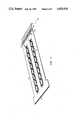
- FIG. 1is a perspective view of an exemplary sub-array assembly including a plurality of multi-layer detector array connecting modules formed in accordance with the present invention.
- FIG. 2is a perspective view of a single module of the subassembly illustrated at FIG. 1.
- FIG. 3is an exploded view of a portion of the module of FIG. 2 illustrating the interface between the individual modules, the detector array portion and the module back plane.
- FIG. 4is an enlarged perspective view of a pair of electronic devices mounted on a module layer, showing exemplary connections thereto.
- FIG. 5is an exploded view of a portion of the module of FIG. 1 illustrating exemplary connections between module layers and the module back plane.
- FIG. 6is an elevational view of a cross-section of an exemplary module illustrating connections to and between electronic devices mounted on different substrate layers.
- FIG. 7is a perspective view of a module construction incorporating an alternate electronic interconnect.
- FIG. 1wherein there is shown a detector subarray including a plurality of modules 11 that may be formed in accordance with the present invention.
- Sub-array 10is connected on one end to a detector array portion 15 and on an opposite end to a connector 17 adapted to interface the subarray to external electronics (not shown).
- Information relating to various aspects of the construction of modular infrared detection systemsis disclosed in U.S. Pat. Nos. 4,304,624; 4,352,715; and 4,354,107 to Carson, et al. It is to be understood, however, that the present invention is not intended to be limited to use in connection with a particular shape of module or design of detector array.
- the unique technique described herein for interconnecting the electronic devices mounted within module 11 and connecting those devices to external electronicsis believed to have application well beyond the particular embodiment described and illustrated herein.
- Each module 11is a stacked laminated structure that provides separate attachment interfaces for detector elements and external electronics.
- the surface of the stacked layers 13provides area for on-focal plane signal processing by integrated circuits or other active or passive electronic devices 19.
- Devices 19may be active or passive electronic components. In the presently preferred embodiment devices 19 comprise identical integrated circuits.
- Each layer 13 within module 11is formed as a thin film of a non-conductive material, such as alumina, with adhesive sheets 24 interposed between layers.
- Each layerpreferably has a delineated metal circuit pattern on a major surface thereof which serves to facilitate necessary connections between electronic devices, detector elements and external electronics.
- the conductive metal patternsmay be disposed on one or both sides of the layers.
- Each layer 13 of module 11typically supports a pattern of metalized conductors, a first portion of which is adapted to connect a dedicated row of detector elements in abutting array portion 15 to electronic devices 19 mounted on the same or a different layer, and a second portion of which connects electronic devices to other electronic devices and to an interconnect in communication with external electronics.
- Exemplary conductive patterns formed on the surface of layer 13 for interconnecting the individual detectors to electronic devices 19are illustrated at FIGS. 5 and 6 of the above-referenced Carson patents. It should be noted, however, that various other conductive patterns connecting the detector elements to the electronic devices may be implemented within the scope of the present invention.
- a row of detectors abutting each layer 13serves as inputs to one or more dedicated electronic devices 19 within the module 11.
- the thickness of the layersis typically determined in view of the center line spacing between adjacent detector elements and the structural characteristics of the material used to form the layer.
- the size and construction of modules 11may be determined after the physical constraints and performance requirements of the particular application have been evaluated.
- cavitiessuch as cavities 21 and 23 may be formed in one or more of the layers 13 with the devices 19 mounted on layers offset from the layer supporting the respective input circuitry. It should be noted that devices 19 need not all be mounted on the same layer, and may be mounted at stepped levels within the module or on opposite sides of the center of the module, as shown at FIG. 6. Moreover, where the devices are formed to be approximately the thickness of layers 13 the devices may be mounted within openings in the layers, thereby eliminating the need for cavities in adjacent layers.
- the module layerssupport conductive patterns, a portion of which facilitates connections between a row of detector elements and a pair of dedicated devices 19 disposed one each within channels 21 and 23, equidistant from the detector elements.
- each device 19may include 64 channels or more, each channel being identical and dedicated to an individual detector element on the associated row of the array portion 15.
- the conductive patterns to support connections between the detector elements and electronic devicesare partially illustrated at FIG. 3 wherein it is shown that conductive patterns 25, 27 and 29 extend to different positions along the length of modules 13.
- each layer 13, to the right of conductive portions 25, 27 and 29,is largely unused.
- interconnections among devices 19, and between devices 19 and external electronicsare typically implemented on a bottom layer that supports the devices 19.
- the arrangement of the output connections from all devices 19 to external electronicshad been formed along the surface of a single layer, i.e. the same layer supporting devices 19, and therefore results in undue congestion on that layer and consequently introduces potential performance problems.
- the present inventionpermits the electronic devices to be formed on a plurality of layers connected to each other and to external electronics by conductive patterns formed on a plurality of the module layers with conductors extending transverse to the plane of the layers.
- the transverse conductorsmay be implemented in conjunction with a transverse back plane 33 adapted to interconnect the electronic devices and external electronics.
- the inventionpermits greater utilization of the module space to support connections between the devices and external electronics, and thereby increases the module space practically available to support on focal plane processing on one or more of the layers.
- FIG. 4illustrates one manner of connecting devices 19 to conductive patterns formed on a single supporting layer 13. Connections to and from the devices are effected using wire bonds 28 bridging the devices and conductors 30, 31 and 32 on layer 13. Though it may be practical in some applications to form all connections between devices 19 and external electronics on a single layer, e.g. where only a small number of devices are arranged in a single row, variations in the arrangement of the devices as well as increases in the number and sophistication of devices 19 will require additional surface area to support the wiring.
- FIGS. 5 and 6illustrate alternative embodiments of the present invention which illustrate constructions for effecting connections among devices 19, and between devices 19 and external electronics.
- the devices and the conductive patternsmay be distributed among the substrate layers to permit the most efficient use of the module space.
- the illustrated embodimentsutilize conductive patterns formed on a plurality of layers in conjunction with the use of transverse conductive connectors and/or a complementary conductive pattern formed on a back plane 33 disposed transverse to the plane of the layers.
- the present inventionfacilitates inter-device connections along a single layer, or between layers.
- Conductive connections between layersmay be implemented by means of wire bonds, vias 35, 37, or by means of metalized regions 39 and 41 disposed on back plane 33. At least some of the metallized regions are in turn connected to conductors 49 that lead to the external electronics.
- the inventionthus permits interconnections to be made within the module body transverse to the plane of the layers, along the surface of the layers, or along the back plane.
- the precise combination of conductive patterns on and interconnecting each layer 13,is a matter of design choice in view of processing requirements, conductor density, detector element spacing, layer thickness, and interconnection requirements in a particular application.
- FIG. 5illustrates simplified conductive patterns intended to represent only a few of the types of connections that may be implemented within the scope of the present invention.
- connections to and from devices 19may be made along a single layer, such as shown on the surface of layer 13a interconnecting devices 19b and 19f.
- each device 19may be mounted on or connected to a different layer, and interconnected by means of a via, such as via 37 connecting device 19f and device 19e mounted on layers 13a and 13c, respectively.
- connections to numerous devicesmay be effected by connecting a back plane conductive region to a conductive via 35, connecting devices such as devices 19d, 19e and 19f on layers 13c, 13b and 13a, respectively.
- connecting devicessuch as devices 19d, 19e and 19f on layers 13c, 13b and 13a, respectively.
- connectionsmay be facilitated by a conductive region 39 disposed on back plane 33 (enlarged for illustrative purposes), connecting devices, such as 19a, 19b and 19c on layers 13c, 13b and 13a, respectively.
- Such an alternativemay be desirable, for example, where it is unnecessary to connect intermediate layers and, therefore, the space on the intermediate layers may be more advantageously devoted to supporting additional electronic devices.
- connective region 41on back plane 33, may be used to connect devices such as 19a and 19d even though each device is connected to a common layer, such as 13c. That variation may be preferable, for example, where the surface area intermediate devices 19a and 19d is occupied with other conductors.
- Other three-dimensional conductive connecting patternsmay be designed to make the best use of available space in view of the connection requirements and may be implemented within the scope of the present invention.
- module 13may be formed to include a plurality of electronic device supporting layers in back-to-back relation with connections to detector elements or between devices 19 affected by means of conductive vias such as vias 43 and 44 extending through module center layers 13d and 13e, or by means of common connection to conductive regions 49 and 47 formed on back plane 33.
- conductive viassuch as vias 43 and 44 extending through module center layers 13d and 13e, or by means of common connection to conductive regions 49 and 47 formed on back plane 33.
- detector element interconnectors 51are formed along an edge portion of the module.
- the connectors 51are connectable to corresponding detector elements within detector array 15 (shown at FIG. 3).
- Interconnections between devices 19 and a first portion of the conductive patterns leading to the detector elementsare effected by wire bonds 24, 26, 28, 34, 36, 38, 40 and 42.
- Insulating layer 50separates layers 13d and 13e, thereby permitting conductive patterns to be formed on the opposing surfaces of those layers.
- Interconnections between devices 19, and between those devices and external electronicsare effected by wire bonds 52, 54, 56 and 58 connecting the devices to portions of the conductive pattern which are in turn connected to conductive regions 47 and 49 on the backplane 33. Interconnections may be effected using conductive patterns formed on any layer.
- FIG. 7illustrates another embodiment of the invention wherein two rows of devices 19 are provided on one side of the module, with one or two similar rows provided on the opposite side of the center layer.
- Each rowis serviced by a separate but identical bus (not shown) provided under the device supporting layers.
- Each buscommunicates signals between a plurality of devices 19 and the interconnect 61 to external electronics.
- the bus linesare connected to conductive patterns on different layers by wire bonds 55 and 53.
- the conductive patterns on those layersare arranged such that the conductors to each bus are brought to substantially overlapping registry in the same signal sequence.
- the conductorsmay then be connected to each other, and to external interconnect 61 by means such as wire bonds 57 and 59.
- connectionsare effected by an interconnect 61 comprised of a plurality of discrete conductive strips 62, 64 and 66, formed on one or more surfaces of the layers 13.
- the conductive stripsmay thereby be connected to conductive patterns on the surface of the supporting layer as well as on the surface of upper and lower layers. If desired, additional layers may be provided with such conductive strips.
- the individual layers 13are first profiled to the desired shape and opening pattern (if necessary) to provide space for the electronic devices.
- a metalized patternis thereafter deposited onto the surface of each layer using techniques such as photo-delineation of the desired pattern.
- Each layeris provided with a sheet of adhesive shaped to conform with the shape of the layers.
- Each layer with an adhesive sheet appliedmay then be heated in an oven for a time and at a layer using techniques such as photo-delineation of the desired pattern.
- Each layeris provided with a sheet of adhesive shaped to conform with the shape of the layers.
- Each layer with an adhesive sheet appliedmay then be heated in an oven for a time and at a temperature to provide adherence without curing of the adhesive. Subsequently, the adhesive sheet may be further trimmed to the profile of the layer to which it has been applied.
- the layersare then stacked upon a male fixture, coated with a parting agent, in the order in which the module is to be formed.
- a similarly coated female fixtureis overlapped upon the completed stack, and joins the male fixture to minimize rotation of the layers within the fixtures.
- a shimis placed between the male and female fixtures to control the finished module thickness to a dimension consistent with vertical stackability.
- the fixtured assemblyis then placed in a laminating press and subjected to a temperature and pressure cycle that fully cures the adhesive bonds between the layers.
- the moduleis then cooled, removed from the fixture, and excessive adhesive is then removed. After the epoxy is then cured and the excess cleaned the module is machined by a process such as diamond grinding.
- the machining processserves to expose the conductive patterns for connections and to conform the dimensions of the module to dimensions consistent with lateral abuttment with similar modules.
- Conductive padsmay be photodelineated on the ends of the module to facilitate connection between the metalized pattern on each layer and a dedicated detector or back plane portion.
- Vias to connect conductive patterns on different layers within the module 11may be formed by various means.
- One technique of forming the viasis to drill holes through the layers by means of a laser drill and to deposit metal on and through the holes by means of metal sputtering techniques.
- each layer 13is formed to have a length, l, of approximately 2.9 inches, a width w of approximately 1.024 inches and a thickness t of approximately 0.004 inches. Eight of such layers are then stacked to form a module approximately 0.032 inches thick. In turn, thirty-two modules are stacked to form a subarray, approximately 1.024 inches thick. Twenty-five sub-arrays may, for example, be placed adjacent to each other (five subarrays on a side), and bump bonded together to form a small square array.
Landscapes
- Physics & Mathematics (AREA)
- Condensed Matter Physics & Semiconductors (AREA)
- General Physics & Mathematics (AREA)
- Engineering & Computer Science (AREA)
- Computer Hardware Design (AREA)
- Microelectronics & Electronic Packaging (AREA)
- Power Engineering (AREA)
- Solid State Image Pick-Up Elements (AREA)
Abstract
Description
Claims (17)
Priority Applications (1)
| Application Number | Priority Date | Filing Date | Title |
|---|---|---|---|
| US06/731,988US4659931A (en) | 1985-05-08 | 1985-05-08 | High density multi-layered integrated circuit package |
Applications Claiming Priority (1)
| Application Number | Priority Date | Filing Date | Title |
|---|---|---|---|
| US06/731,988US4659931A (en) | 1985-05-08 | 1985-05-08 | High density multi-layered integrated circuit package |
Publications (1)
| Publication Number | Publication Date |
|---|---|
| US4659931Atrue US4659931A (en) | 1987-04-21 |
Family
ID=24941736
Family Applications (1)
| Application Number | Title | Priority Date | Filing Date |
|---|---|---|---|
| US06/731,988Expired - LifetimeUS4659931A (en) | 1985-05-08 | 1985-05-08 | High density multi-layered integrated circuit package |
Country Status (1)
| Country | Link |
|---|---|
| US (1) | US4659931A (en) |
Cited By (46)
| Publication number | Priority date | Publication date | Assignee | Title |
|---|---|---|---|---|
| US4737659A (en)* | 1986-01-27 | 1988-04-12 | Siemens-Albis Aktiengesellschaft | Controlled switching array |
| US4755681A (en)* | 1986-09-30 | 1988-07-05 | Shimadzu Corporation | Radiation image detecting apparatus with IC modules stacked stepwise |
| US4792672A (en)* | 1985-04-12 | 1988-12-20 | Grumman Aerospace Corporation | Detector buffer board |
| US4845313A (en)* | 1985-07-22 | 1989-07-04 | Tokyo Communication Equipment Co., Ltd. | Metallic core wiring substrate |
| US4891522A (en)* | 1988-10-11 | 1990-01-02 | Microtronics Associates, Inc. | Modular multi-element high energy particle detector |
| US4949225A (en)* | 1987-11-10 | 1990-08-14 | Ibiden Co., Ltd. | Circuit board for mounting electronic components |
| US4974317A (en)* | 1988-09-12 | 1990-12-04 | Westinghouse Electric Corp. | Method of making for RF line replacable modules |
| US4988641A (en)* | 1989-10-10 | 1991-01-29 | Grumman Aerospace Corporation | Graphotaxially forming a photosensitive detector array |
| US5013919A (en)* | 1989-10-17 | 1991-05-07 | Grumman Aerospace Corporation | Detector element signal comparator system |
| US5013687A (en)* | 1989-07-27 | 1991-05-07 | Grumman Aerospace Corporation | Framed chip hybrid stacked layer assembly |
| US5030828A (en)* | 1990-06-25 | 1991-07-09 | Grumman Aerospace Corporation | Recessed element photosensitive detector array with optical isolation |
| US5075238A (en)* | 1990-04-13 | 1991-12-24 | Grumman Aerospace Corporation | Detector interface device |
| US5093708A (en)* | 1990-08-20 | 1992-03-03 | Grumman Aerospace Corporation | Multilayer integrated circuit module |
| US5128749A (en)* | 1991-04-08 | 1992-07-07 | Grumman Aerospace Corporation | Fused high density multi-layer integrated circuit module |
| US5135556A (en)* | 1991-04-08 | 1992-08-04 | Grumman Aerospace Corporation | Method for making fused high density multi-layer integrated circuit module |
| US5138164A (en)* | 1991-07-15 | 1992-08-11 | Grumman Aerospace Corporation | Infrared detector subarray with integral optical filter |
| WO1992015062A1 (en)* | 1991-02-06 | 1992-09-03 | Irvine Sensors Corporation | Hardware for electronic neural network |
| US5231304A (en)* | 1989-07-27 | 1993-07-27 | Grumman Aerospace Corporation | Framed chip hybrid stacked layer assembly |
| US5315147A (en)* | 1989-09-25 | 1994-05-24 | Grumman Aerospace Corporation | Monolithic focal plane array |
| US5319159A (en)* | 1992-12-15 | 1994-06-07 | Sony Corporation | Double-sided printed wiring board and method of manufacture thereof |
| US5418690A (en)* | 1993-06-11 | 1995-05-23 | International Business Machines Corporation | Multiple wiring and X section printed circuit board technique |
| US5657206A (en)* | 1994-06-23 | 1997-08-12 | Cubic Memory, Inc. | Conductive epoxy flip-chip package and method |
| US5661087A (en)* | 1994-06-23 | 1997-08-26 | Cubic Memory, Inc. | Vertical interconnect process for silicon segments |
| US5698895A (en)* | 1994-06-23 | 1997-12-16 | Cubic Memory, Inc. | Silicon segment programming method and apparatus |
| US5856235A (en)* | 1995-04-12 | 1999-01-05 | Northrop Grumman Corporation | Process of vacuum annealing a thin film metallization on high purity alumina |
| US5891761A (en)* | 1994-06-23 | 1999-04-06 | Cubic Memory, Inc. | Method for forming vertical interconnect process for silicon segments with thermally conductive epoxy preform |
| US6080596A (en)* | 1994-06-23 | 2000-06-27 | Cubic Memory Inc. | Method for forming vertical interconnect process for silicon segments with dielectric isolation |
| US6124633A (en)* | 1994-06-23 | 2000-09-26 | Cubic Memory | Vertical interconnect process for silicon segments with thermally conductive epoxy preform |
| US6255726B1 (en) | 1994-06-23 | 2001-07-03 | Cubic Memory, Inc. | Vertical interconnect process for silicon segments with dielectric isolation |
| US6486528B1 (en) | 1994-06-23 | 2002-11-26 | Vertical Circuits, Inc. | Silicon segment programming apparatus and three terminal fuse configuration |
| US20040188596A1 (en)* | 2003-03-28 | 2004-09-30 | Ludwig David E. | Three-dimensional imaging device incorporating stacked layers containing microelectronic circuits |
| US20050051733A1 (en)* | 2003-06-06 | 2005-03-10 | Unaxis Balzers Ltd. | Optical device for surface-generated fluorescence |
| US20050224952A1 (en)* | 2004-04-13 | 2005-10-13 | Al Vindasius | Three dimensional six surface conformal die coating |
| US20050258530A1 (en)* | 2004-04-13 | 2005-11-24 | Al Vindasius | Micropede stacked die component assembly |
| US7180579B1 (en)* | 2003-03-28 | 2007-02-20 | Irvine Sensors Corp. | Three-dimensional imaging processing module incorporating stacked layers containing microelectronic circuits |
| US20070052084A1 (en)* | 2005-08-26 | 2007-03-08 | Kennedy John V | High density interconnect assembly comprising stacked electronic module |
| US7215018B2 (en) | 2004-04-13 | 2007-05-08 | Vertical Circuits, Inc. | Stacked die BGA or LGA component assembly |
| US7436494B1 (en) | 2003-03-28 | 2008-10-14 | Irvine Sensors Corp. | Three-dimensional ladar module with alignment reference insert circuitry |
| US20110032130A1 (en)* | 2009-08-06 | 2011-02-10 | Irvine Sensors Corporation | AM chirp LADAR readout circuit and module |
| US20110032508A1 (en)* | 2009-08-06 | 2011-02-10 | Irvine Sensors Corporation | Phase sensing and scanning time of flight LADAR using atmospheric absorption bands |
| US20110176579A1 (en)* | 2006-03-14 | 2011-07-21 | International Business Machines Corporation | Multi-layered thermal sensor for integrated circuits and other layered structures |
| US8198576B2 (en) | 2003-03-28 | 2012-06-12 | Aprolase Development Co., Llc | Three-dimensional LADAR module with alignment reference insert circuitry comprising high density interconnect structure |
| US20120161010A1 (en)* | 2009-09-22 | 2012-06-28 | Irvine Sensors Corporations | Stacked Micro-channel Plate Assembly Comprising a Micro-lens |
| US20120170029A1 (en)* | 2009-09-22 | 2012-07-05 | ISC8 Inc. | LIDAR System Comprising Large Area Micro-Channel Plate Focal Plane Array |
| US20120170024A1 (en)* | 2009-09-22 | 2012-07-05 | Medhat Azzazy | Long Range Acquisition and Tracking SWIR Sensor System Comprising Micro-Lamellar Spectrometer |
| US20120181433A1 (en)* | 2009-09-22 | 2012-07-19 | Irvine Sensors Corporation | Sensor System Comprising Stacked Micro-Channel Plate Detector |
Citations (26)
| Publication number | Priority date | Publication date | Assignee | Title |
|---|---|---|---|---|
| US3349162A (en)* | 1965-08-23 | 1967-10-24 | Automatic Elect Lab | Intra-connection techniques for multilayer printed wiring boards |
| US3349481A (en)* | 1964-12-29 | 1967-10-31 | Alpha Microelectronics Company | Integrated circuit sealing method and structure |
| US3400210A (en)* | 1966-04-26 | 1968-09-03 | Automatic Elect Lab | Interlayer connection technique for multilayer printed wiring boards |
| US3403300A (en)* | 1966-09-01 | 1968-09-24 | Magnavox Co | Electronic module |
| US3436604A (en)* | 1966-04-25 | 1969-04-01 | Texas Instruments Inc | Complex integrated circuit array and method for fabricating same |
| US3483308A (en)* | 1968-10-24 | 1969-12-09 | Texas Instruments Inc | Modular packages for semiconductor devices |
| US3499218A (en)* | 1966-10-31 | 1970-03-10 | Electro Mechanisms Inc | Multilayer circuit boards and methods of making the same |
| US3601522A (en)* | 1970-06-18 | 1971-08-24 | American Lava Corp | Composite ceramic package breakaway notch |
| US3634600A (en)* | 1969-07-22 | 1972-01-11 | Ceramic Metal Systems Inc | Ceramic package |
| US3705332A (en)* | 1970-06-25 | 1972-12-05 | Howard L Parks | Electrical circuit packaging structure and method of fabrication thereof |
| US3760090A (en)* | 1971-08-19 | 1973-09-18 | Globe Union Inc | Electronic circuit package and method for making same |
| US3777221A (en)* | 1972-12-18 | 1973-12-04 | Ibm | Multi-layer circuit package |
| US3852714A (en)* | 1972-06-22 | 1974-12-03 | Eocom Corp | Adaptive imaging system |
| US3875479A (en)* | 1973-05-07 | 1975-04-01 | Gilbert R Jaggar | Electrical apparatus |
| US3917983A (en)* | 1973-11-12 | 1975-11-04 | Bunker Ramo | Multiwafer electrical circuit construction and method of making |
| US3926746A (en)* | 1973-10-04 | 1975-12-16 | Minnesota Mining & Mfg | Electrical interconnection for metallized ceramic arrays |
| US3970990A (en)* | 1972-06-22 | 1976-07-20 | Grumman Aerospace Corporation | Adaptive imaging system |
| US4249302A (en)* | 1978-12-28 | 1981-02-10 | Ncr Corporation | Multilayer printed circuit board |
| US4283755A (en)* | 1980-02-05 | 1981-08-11 | The United States Of America As Represented By The Secretary Of The Air Force | Modulator multilayer detector |
| US4288841A (en)* | 1979-09-20 | 1981-09-08 | Bell Telephone Laboratories, Incorporated | Double cavity semiconductor chip carrier |
| US4304624A (en)* | 1977-11-28 | 1981-12-08 | Irvine Sensors Corporation | Method of fabricating a multi-layer structure for detector array module |
| US4320438A (en)* | 1980-05-15 | 1982-03-16 | Cts Corporation | Multi-layer ceramic package |
| US4352715A (en)* | 1977-11-28 | 1982-10-05 | Irvine Sensors Corporation | Detector array module fabrication |
| US4354107A (en)* | 1977-11-28 | 1982-10-12 | Irvine Sensors Corporation | Detector array module-structure and fabrication |
| US4371744A (en)* | 1977-10-03 | 1983-02-01 | Compagnie Internationale Pour L'informatique Cii-Honeywell Bull (Societe Anonyme) | Substrate for interconnecting electronic integrated circuit components having a repair arrangement enabling modification of connections to a mounted chip device |
| US4423468A (en)* | 1980-10-01 | 1983-12-27 | Motorola, Inc. | Dual electronic component assembly |
- 1985
- 1985-05-08USUS06/731,988patent/US4659931A/ennot_activeExpired - Lifetime
Patent Citations (26)
| Publication number | Priority date | Publication date | Assignee | Title |
|---|---|---|---|---|
| US3349481A (en)* | 1964-12-29 | 1967-10-31 | Alpha Microelectronics Company | Integrated circuit sealing method and structure |
| US3349162A (en)* | 1965-08-23 | 1967-10-24 | Automatic Elect Lab | Intra-connection techniques for multilayer printed wiring boards |
| US3436604A (en)* | 1966-04-25 | 1969-04-01 | Texas Instruments Inc | Complex integrated circuit array and method for fabricating same |
| US3400210A (en)* | 1966-04-26 | 1968-09-03 | Automatic Elect Lab | Interlayer connection technique for multilayer printed wiring boards |
| US3403300A (en)* | 1966-09-01 | 1968-09-24 | Magnavox Co | Electronic module |
| US3499218A (en)* | 1966-10-31 | 1970-03-10 | Electro Mechanisms Inc | Multilayer circuit boards and methods of making the same |
| US3483308A (en)* | 1968-10-24 | 1969-12-09 | Texas Instruments Inc | Modular packages for semiconductor devices |
| US3634600A (en)* | 1969-07-22 | 1972-01-11 | Ceramic Metal Systems Inc | Ceramic package |
| US3601522A (en)* | 1970-06-18 | 1971-08-24 | American Lava Corp | Composite ceramic package breakaway notch |
| US3705332A (en)* | 1970-06-25 | 1972-12-05 | Howard L Parks | Electrical circuit packaging structure and method of fabrication thereof |
| US3760090A (en)* | 1971-08-19 | 1973-09-18 | Globe Union Inc | Electronic circuit package and method for making same |
| US3852714A (en)* | 1972-06-22 | 1974-12-03 | Eocom Corp | Adaptive imaging system |
| US3970990A (en)* | 1972-06-22 | 1976-07-20 | Grumman Aerospace Corporation | Adaptive imaging system |
| US3777221A (en)* | 1972-12-18 | 1973-12-04 | Ibm | Multi-layer circuit package |
| US3875479A (en)* | 1973-05-07 | 1975-04-01 | Gilbert R Jaggar | Electrical apparatus |
| US3926746A (en)* | 1973-10-04 | 1975-12-16 | Minnesota Mining & Mfg | Electrical interconnection for metallized ceramic arrays |
| US3917983A (en)* | 1973-11-12 | 1975-11-04 | Bunker Ramo | Multiwafer electrical circuit construction and method of making |
| US4371744A (en)* | 1977-10-03 | 1983-02-01 | Compagnie Internationale Pour L'informatique Cii-Honeywell Bull (Societe Anonyme) | Substrate for interconnecting electronic integrated circuit components having a repair arrangement enabling modification of connections to a mounted chip device |
| US4354107A (en)* | 1977-11-28 | 1982-10-12 | Irvine Sensors Corporation | Detector array module-structure and fabrication |
| US4304624A (en)* | 1977-11-28 | 1981-12-08 | Irvine Sensors Corporation | Method of fabricating a multi-layer structure for detector array module |
| US4352715A (en)* | 1977-11-28 | 1982-10-05 | Irvine Sensors Corporation | Detector array module fabrication |
| US4249302A (en)* | 1978-12-28 | 1981-02-10 | Ncr Corporation | Multilayer printed circuit board |
| US4288841A (en)* | 1979-09-20 | 1981-09-08 | Bell Telephone Laboratories, Incorporated | Double cavity semiconductor chip carrier |
| US4283755A (en)* | 1980-02-05 | 1981-08-11 | The United States Of America As Represented By The Secretary Of The Air Force | Modulator multilayer detector |
| US4320438A (en)* | 1980-05-15 | 1982-03-16 | Cts Corporation | Multi-layer ceramic package |
| US4423468A (en)* | 1980-10-01 | 1983-12-27 | Motorola, Inc. | Dual electronic component assembly |
Cited By (68)
| Publication number | Priority date | Publication date | Assignee | Title |
|---|---|---|---|---|
| US4792672A (en)* | 1985-04-12 | 1988-12-20 | Grumman Aerospace Corporation | Detector buffer board |
| US4845313A (en)* | 1985-07-22 | 1989-07-04 | Tokyo Communication Equipment Co., Ltd. | Metallic core wiring substrate |
| US4737659A (en)* | 1986-01-27 | 1988-04-12 | Siemens-Albis Aktiengesellschaft | Controlled switching array |
| US4755681A (en)* | 1986-09-30 | 1988-07-05 | Shimadzu Corporation | Radiation image detecting apparatus with IC modules stacked stepwise |
| US4949225A (en)* | 1987-11-10 | 1990-08-14 | Ibiden Co., Ltd. | Circuit board for mounting electronic components |
| US4974317A (en)* | 1988-09-12 | 1990-12-04 | Westinghouse Electric Corp. | Method of making for RF line replacable modules |
| EP0365203A3 (en)* | 1988-10-11 | 1991-03-06 | Microtronics Associates, Inc. | Modular multi-element high energy particle detector |
| US4891522A (en)* | 1988-10-11 | 1990-01-02 | Microtronics Associates, Inc. | Modular multi-element high energy particle detector |
| US5231304A (en)* | 1989-07-27 | 1993-07-27 | Grumman Aerospace Corporation | Framed chip hybrid stacked layer assembly |
| US5013687A (en)* | 1989-07-27 | 1991-05-07 | Grumman Aerospace Corporation | Framed chip hybrid stacked layer assembly |
| US5315147A (en)* | 1989-09-25 | 1994-05-24 | Grumman Aerospace Corporation | Monolithic focal plane array |
| US4988641A (en)* | 1989-10-10 | 1991-01-29 | Grumman Aerospace Corporation | Graphotaxially forming a photosensitive detector array |
| US5013919A (en)* | 1989-10-17 | 1991-05-07 | Grumman Aerospace Corporation | Detector element signal comparator system |
| EP0454804A4 (en)* | 1989-10-17 | 1993-09-08 | Grumman Aerospace Corporation | Detector element signal comparator system |
| US5075238A (en)* | 1990-04-13 | 1991-12-24 | Grumman Aerospace Corporation | Detector interface device |
| US5030828A (en)* | 1990-06-25 | 1991-07-09 | Grumman Aerospace Corporation | Recessed element photosensitive detector array with optical isolation |
| US5093708A (en)* | 1990-08-20 | 1992-03-03 | Grumman Aerospace Corporation | Multilayer integrated circuit module |
| WO1992015062A1 (en)* | 1991-02-06 | 1992-09-03 | Irvine Sensors Corporation | Hardware for electronic neural network |
| US5235672A (en)* | 1991-02-06 | 1993-08-10 | Irvine Sensors Corporation | Hardware for electronic neural network |
| US5135556A (en)* | 1991-04-08 | 1992-08-04 | Grumman Aerospace Corporation | Method for making fused high density multi-layer integrated circuit module |
| US5128749A (en)* | 1991-04-08 | 1992-07-07 | Grumman Aerospace Corporation | Fused high density multi-layer integrated circuit module |
| US5138164A (en)* | 1991-07-15 | 1992-08-11 | Grumman Aerospace Corporation | Infrared detector subarray with integral optical filter |
| US5319159A (en)* | 1992-12-15 | 1994-06-07 | Sony Corporation | Double-sided printed wiring board and method of manufacture thereof |
| US5418690A (en)* | 1993-06-11 | 1995-05-23 | International Business Machines Corporation | Multiple wiring and X section printed circuit board technique |
| US6188126B1 (en) | 1994-06-23 | 2001-02-13 | Cubic Memory Inc. | Vertical interconnect process for silicon segments |
| US6255726B1 (en) | 1994-06-23 | 2001-07-03 | Cubic Memory, Inc. | Vertical interconnect process for silicon segments with dielectric isolation |
| US5675180A (en)* | 1994-06-23 | 1997-10-07 | Cubic Memory, Inc. | Vertical interconnect process for silicon segments |
| US5698895A (en)* | 1994-06-23 | 1997-12-16 | Cubic Memory, Inc. | Silicon segment programming method and apparatus |
| US5837566A (en)* | 1994-06-23 | 1998-11-17 | Cubic Memory, Inc. | Vertical interconnect process for silicon segments |
| US6486528B1 (en) | 1994-06-23 | 2002-11-26 | Vertical Circuits, Inc. | Silicon segment programming apparatus and three terminal fuse configuration |
| US5891761A (en)* | 1994-06-23 | 1999-04-06 | Cubic Memory, Inc. | Method for forming vertical interconnect process for silicon segments with thermally conductive epoxy preform |
| US5994170A (en)* | 1994-06-23 | 1999-11-30 | Cubic Memory, Inc. | Silicon segment programming method |
| US6080596A (en)* | 1994-06-23 | 2000-06-27 | Cubic Memory Inc. | Method for forming vertical interconnect process for silicon segments with dielectric isolation |
| US6124633A (en)* | 1994-06-23 | 2000-09-26 | Cubic Memory | Vertical interconnect process for silicon segments with thermally conductive epoxy preform |
| US5657206A (en)* | 1994-06-23 | 1997-08-12 | Cubic Memory, Inc. | Conductive epoxy flip-chip package and method |
| US5661087A (en)* | 1994-06-23 | 1997-08-26 | Cubic Memory, Inc. | Vertical interconnect process for silicon segments |
| US5856235A (en)* | 1995-04-12 | 1999-01-05 | Northrop Grumman Corporation | Process of vacuum annealing a thin film metallization on high purity alumina |
| US20040188596A1 (en)* | 2003-03-28 | 2004-09-30 | Ludwig David E. | Three-dimensional imaging device incorporating stacked layers containing microelectronic circuits |
| USRE43722E1 (en) | 2003-03-28 | 2012-10-09 | Aprolase Development Co., Llc | Three-dimensional ladar module with alignment reference insert circuitry |
| US8198576B2 (en) | 2003-03-28 | 2012-06-12 | Aprolase Development Co., Llc | Three-dimensional LADAR module with alignment reference insert circuitry comprising high density interconnect structure |
| US7180579B1 (en)* | 2003-03-28 | 2007-02-20 | Irvine Sensors Corp. | Three-dimensional imaging processing module incorporating stacked layers containing microelectronic circuits |
| US7436494B1 (en) | 2003-03-28 | 2008-10-14 | Irvine Sensors Corp. | Three-dimensional ladar module with alignment reference insert circuitry |
| US20070052947A1 (en)* | 2003-03-28 | 2007-03-08 | Ludwig David E | Three-dimensional imaging processing module incorporating stacked layers containing microelectronic circuits |
| US20050051733A1 (en)* | 2003-06-06 | 2005-03-10 | Unaxis Balzers Ltd. | Optical device for surface-generated fluorescence |
| US7285789B2 (en)* | 2003-06-06 | 2007-10-23 | Oc Oerlikon Balzers Ag | Optical device for surface-generated fluorescence |
| US7245021B2 (en) | 2004-04-13 | 2007-07-17 | Vertical Circuits, Inc. | Micropede stacked die component assembly |
| US20050258530A1 (en)* | 2004-04-13 | 2005-11-24 | Al Vindasius | Micropede stacked die component assembly |
| US20070284716A1 (en)* | 2004-04-13 | 2007-12-13 | Vertical Circuits, Inc. | Assembly Having Stacked Die Mounted On Substrate |
| US20070290377A1 (en)* | 2004-04-13 | 2007-12-20 | Vertical Circuits, Inc. | Three Dimensional Six Surface Conformal Die Coating |
| US8729690B2 (en) | 2004-04-13 | 2014-05-20 | Invensas Corporation | Assembly having stacked die mounted on substrate |
| US7535109B2 (en) | 2004-04-13 | 2009-05-19 | Vertical Circuits, Inc. | Die assembly having electrical interconnect |
| US7705432B2 (en) | 2004-04-13 | 2010-04-27 | Vertical Circuits, Inc. | Three dimensional six surface conformal die coating |
| US8357999B2 (en) | 2004-04-13 | 2013-01-22 | Vertical Circuits (Assignment For The Benefit Of Creditors), Llc | Assembly having stacked die mounted on substrate |
| US20050224952A1 (en)* | 2004-04-13 | 2005-10-13 | Al Vindasius | Three dimensional six surface conformal die coating |
| US7215018B2 (en) | 2004-04-13 | 2007-05-08 | Vertical Circuits, Inc. | Stacked die BGA or LGA component assembly |
| US20070052084A1 (en)* | 2005-08-26 | 2007-03-08 | Kennedy John V | High density interconnect assembly comprising stacked electronic module |
| US8425115B2 (en)* | 2006-03-14 | 2013-04-23 | International Business Machines Corporation | Multi-layered thermal sensor for integrated circuits and other layered structures |
| US20110176579A1 (en)* | 2006-03-14 | 2011-07-21 | International Business Machines Corporation | Multi-layered thermal sensor for integrated circuits and other layered structures |
| US8279420B2 (en) | 2009-08-06 | 2012-10-02 | ISC8 Inc. | Phase sensing and scanning time of flight LADAR using atmospheric absorption bands |
| US8125367B2 (en) | 2009-08-06 | 2012-02-28 | Irvine Sensors Corp. | AM chirp LADAR readout circuit and module |
| US20110032508A1 (en)* | 2009-08-06 | 2011-02-10 | Irvine Sensors Corporation | Phase sensing and scanning time of flight LADAR using atmospheric absorption bands |
| US20110032130A1 (en)* | 2009-08-06 | 2011-02-10 | Irvine Sensors Corporation | AM chirp LADAR readout circuit and module |
| US20120170024A1 (en)* | 2009-09-22 | 2012-07-05 | Medhat Azzazy | Long Range Acquisition and Tracking SWIR Sensor System Comprising Micro-Lamellar Spectrometer |
| US20120181433A1 (en)* | 2009-09-22 | 2012-07-19 | Irvine Sensors Corporation | Sensor System Comprising Stacked Micro-Channel Plate Detector |
| US20120170029A1 (en)* | 2009-09-22 | 2012-07-05 | ISC8 Inc. | LIDAR System Comprising Large Area Micro-Channel Plate Focal Plane Array |
| US20120161010A1 (en)* | 2009-09-22 | 2012-06-28 | Irvine Sensors Corporations | Stacked Micro-channel Plate Assembly Comprising a Micro-lens |
| US9129780B2 (en)* | 2009-09-22 | 2015-09-08 | Pfg Ip Llc | Stacked micro-channel plate assembly comprising a micro-lens |
| US9142380B2 (en)* | 2009-09-22 | 2015-09-22 | Pfg Ip Llc | Sensor system comprising stacked micro-channel plate detector |
Similar Documents
| Publication | Publication Date | Title |
|---|---|---|
| US4659931A (en) | High density multi-layered integrated circuit package | |
| US4618763A (en) | Infrared focal plane module with stacked IC module body | |
| US5135556A (en) | Method for making fused high density multi-layer integrated circuit module | |
| US4703170A (en) | Infrared focal plane module | |
| US5717247A (en) | Microcircuit via interconnect | |
| US5032896A (en) | 3-D integrated circuit assembly employing discrete chips | |
| US4304624A (en) | Method of fabricating a multi-layer structure for detector array module | |
| US5426566A (en) | Multichip integrated circuit packages and systems | |
| US4983533A (en) | High-density electronic modules - process and product | |
| JP3544974B2 (en) | Integrated laminate | |
| US5093708A (en) | Multilayer integrated circuit module | |
| US4692839A (en) | Multiple chip interconnection system and package | |
| US4195195A (en) | Tape automated bonding test board | |
| US4237522A (en) | Chip package with high capacitance, stacked vlsi/power sheets extending through slots in substrate | |
| EP0520681B1 (en) | Electronic device interconnection technique | |
| US4958258A (en) | Modular hybrid microelectronic structures with high density of integration | |
| US4354107A (en) | Detector array module-structure and fabrication | |
| EP0308465B1 (en) | Detector buffer board | |
| US5621193A (en) | Ceramic edge connect process | |
| US4283755A (en) | Modulator multilayer detector | |
| US5157255A (en) | Compact, thermally efficient focal plane array and testing and repair thereof | |
| US4352715A (en) | Detector array module fabrication | |
| US5128749A (en) | Fused high density multi-layer integrated circuit module | |
| US5209798A (en) | Method of forming a precisely spaced stack of substrate layers | |
| US4807000A (en) | High density small element optical mosaic detector |
Legal Events
| Date | Code | Title | Description |
|---|---|---|---|
| AS | Assignment | Owner name:GRUMMAN AEROSPACE CORPORATION Free format text:ASSIGNMENT OF ASSIGNORS INTEREST.;ASSIGNORS:SCHMITZ, CHARLES E.;WIMBERLY, RICHARD C.;CARLSON, DONALD J.;REEL/FRAME:004445/0168 Effective date:19850425 Owner name:GRUMMAN AEROSPACE CORPORATION Free format text:ASSIGNMENT OF ASSIGNORS INTEREST.;ASSIGNORS:SCHMITZ, CHARLES E.;WIMBERLY, RICHARD C.;CARLSON, DONALD J.;REEL/FRAME:004445/0167 Effective date:19850425 | |
| STCF | Information on status: patent grant | Free format text:PATENTED CASE | |
| FPAY | Fee payment | Year of fee payment:4 | |
| FEPP | Fee payment procedure | Free format text:PAYOR NUMBER ASSIGNED (ORIGINAL EVENT CODE: ASPN); ENTITY STATUS OF PATENT OWNER: LARGE ENTITY | |
| FPAY | Fee payment | Year of fee payment:8 | |
| FEPP | Fee payment procedure | Free format text:PAYER NUMBER DE-ASSIGNED (ORIGINAL EVENT CODE: RMPN); ENTITY STATUS OF PATENT OWNER: LARGE ENTITY Free format text:PAYOR NUMBER ASSIGNED (ORIGINAL EVENT CODE: ASPN); ENTITY STATUS OF PATENT OWNER: LARGE ENTITY | |
| FPAY | Fee payment | Year of fee payment:12 |