US4659874A - X-Y position sensor - Google Patents
X-Y position sensorDownload PDFInfo
- Publication number
- US4659874A US4659874AUS06/779,350US77935085AUS4659874AUS 4659874 AUS4659874 AUS 4659874AUS 77935085 AUS77935085 AUS 77935085AUS 4659874 AUS4659874 AUS 4659874A
- Authority
- US
- United States
- Prior art keywords
- conductors
- pad
- stylus
- edge
- sensing
- Prior art date
- Legal status (The legal status is an assumption and is not a legal conclusion. Google has not performed a legal analysis and makes no representation as to the accuracy of the status listed.)
- Expired - Lifetime
Links
Images
Classifications
- G—PHYSICS
- G06—COMPUTING OR CALCULATING; COUNTING
- G06F—ELECTRIC DIGITAL DATA PROCESSING
- G06F3/00—Input arrangements for transferring data to be processed into a form capable of being handled by the computer; Output arrangements for transferring data from processing unit to output unit, e.g. interface arrangements
- G06F3/01—Input arrangements or combined input and output arrangements for interaction between user and computer
- G06F3/03—Arrangements for converting the position or the displacement of a member into a coded form
- G06F3/041—Digitisers, e.g. for touch screens or touch pads, characterised by the transducing means
- G06F3/044—Digitisers, e.g. for touch screens or touch pads, characterised by the transducing means by capacitive means
- G06F3/0442—Digitisers, e.g. for touch screens or touch pads, characterised by the transducing means by capacitive means using active external devices, e.g. active pens, for transmitting changes in electrical potential to be received by the digitiser
Definitions
- This inventionrelates to a low-cost X-Y position sensor. More particularly it relates to a so called “sketch pad" that transmits to a digital computer signals indicative of the position of a stylus that is manually moved over the surface of a planar sensing pad. Sensing conductors on the pad are formed in a single layer on the pad and the signals induced in them or transmitted by them are sensed by analog circuitry whose output is converted to digital signals representing the X-Y coordinates of the stylus position.
- Electronic sketch padshave long been used to provide inputs to digital computers. They are generally used in an interactive mode in which a cursor on a CRT monitor traces a path corresponding to the path of a stylus moved by an operator over a sensing pad. This arrangement can be used to position the cursor at any desired point on the CRT screen or, alternatively, to draw lines on the screen.
- sketch padsare generally of two types.
- the sensing padcontains two conductor grids, one overlying the other, with the conductors in one grid orthogonal to those in the other grid.
- the wires in one of the gridsare first energized sequentially and the signal picked up by the stylus from the wires is sensed to indicate which of the wires is in closest proximity to the stylus. This fixes the position of the stylus along one axis.
- the wires in the second gridare then sequentially energized to ascertain the stylus position along the other axis.
- This systemis capable of high resolution. However, its cost has significantly limited its applicability.
- the sensing padhas an array of generally parallel pairs of adjacent sensing conductors which, for the purpose of this explanation, will be considered as extending in the horizontal or X direction.
- Each conductorhas a generally triangular shape, with the base of the triangle at one edge of the pad and the apex at the opposite edge.
- the conductors in each pairare complementary, that is, their bases are at opposite edges of the pad.
- the conductorsmay be divided into four sets, a "left” and “right” set and an "ascending” and “descending” set.
- a left setcontaining triangular conductors whose bases are on the left edge of the pad and the apex on the right side and a right set containing triangular conductors whose bases are on the right side and the apex is on the left side.
- the ascending setconsists of a vertical series of left and right pairs of complimentary triangles, generally defining rectangles, whose vertical dimension decreases from a maximum at the upper edge of the sensing pad to a minimum at the lower end.
- the descending setis interleaved with the ascending set and consists of left and right triangular pairs whose vertical dimensions decrease from a maximum at the lower edge of the pad to a minimum at the upper edge.
- the stylus used with the sensing padhas an electrode at its tip to which it applies an alternating current signal at a frequency that is suitably high for capacitive coupling to the sensing pad.
- the right sets or left sets set of conductorsare selectively connected to sensing circuitry and the others of these two sets are selectively grounded.
- the sensed voltagethen corresponds to the X position.
- the energy coupled to the right sets from the signal emitted by the styluscorresponds to the relative widths, i.e. in the Y direction, of the right sets of conductors at the position of the stylus.
- the sensed signalincreases in intensity with the X coordinate of the stylus position.
- the ascending sets of conductorsare connected to the sensing circuitry and the descending sets are grounded. Since the widths of the ascending sets increase from a minimum at the bottom edge of the pad to a maximum at the top edge, the sensed voltage increases with the Y coordinate of the stylus position.
- the X- and Y- coordinate measurementsare independent of each other even though the same conductors are used for both the X and Y measurements. Furthermore the conductors are connected on the sensing pad into four sets, with the switching arranged to select array these four sets for connection to the sensing circuitry. This results in a considerably lower cost than those systems that require selection of individual conductors on the sensing pad. Moreover the conductors on the pad are on a single layer, thereby providing a lower cost than prior multi-layer arrangements.
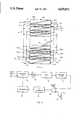
- FIG. 1is a diagram of a sensing pad and stylus used in a position detector embodying the invention.
- FIG. 2is a diagram of sensing circuitry that processes the signals from the sensing pad of FIG. 1.
- a position sensor embodying the inventioncomprises a sensing pad generally indicated at 10 and a stylus 12 whose position on the pad is sensed by means of the invention.
- the pad 10comprises various conductors, described below, which can be formed in a single layer on a suitable substrate (not shown) by conventional etched circuit techniques.
- the stylusincludes an alternationing-current generator that applies an AC signal to an electrode in the tip 12A of the stylus and this signal is capacitively coupled to conductors in a sensing area 10A on the pad 10.
- the conductors in the sensing area 10Acomprise an ascending set 14 1 -14 n and a descending set 16 1 -16 n .
- the conductors 14 and 16are triangular in shape and are arrayed in complementary pairs. In each pair the base of one of the triangles is at the left edge of the sensing area and its apex at the right while the other triangle is disposed in the opposite sense.
- the conductors with their base ends at the left hand edgeconstitute the "left" set.
- These conductorsare designated with the suffix "L”.
- Those with their bases setare designated with the suffix "R”.
- the widths of the conductor pairsi.e.
- the dimension in the Y directionincrease from minimum at the bottom edge of the sensing area 10A to a maximum at the top.
- the widths of the conductor pairs 16 in the descending setdecrease from a maximum at the bottom of the sensing area to a minimum at the top.
- the conductors 14L, 14R, 16L and 16Rare interconnected in four sets which are the intersections of the ascending, descending, right and left sets, namely a right ascending set (RA) consisting of the right hand conductors 14R, a left ascending set (LA)consisting of the conductors 14L, a right descending set (RD) consisting of the conductors 16R and a left descending (LD) set consisting of the conductors 16L.
- the sensing conductors in each of the latter four setsare connected together by means of conductors RA, LA, RD and LD as indicated. These conductors provide terminals for the connections to the sensing pad.
- the outputs of the sensing pad 10are selected, as described below, by a switching unit 18 whose output in turn is fed to an amplifier 20.
- the output of the amplifier 20is rectified by a rectifier 22 whose output is passed through a low pass filter 24 to remove the ripple component thereof.
- the resulting DC signalis passed through an offset amplifier 26 and converted to a digital signal by a digital-analog converter 28.
- the digital signalis then processed by a digital data processor as described below.
- the signal induced in a set of the sensing conductors in the sensing area 10A of the pad 10is essentially proportional to the capacitance between the stylus and that set of conductors, assuming that the circuit of FIG. 2 applies a suitable load impedance to the conductor sets.
- the output voltage of the amplifierwill reflect the capacitance between the stylus and that set of conductors.
- This capacitanceis essentially proportional to the area of that set of conductors in proximity to the tip of the stylus and the area in turn is proportional to the conductor widths in that region.
- the widths of the right-hand conductorsincrease linearly with the X coordinate. Accordingly the coupling capacitance between the stylus and this set of conductors also increases linearly with the X coordinate, as does the output voltage of the amplifier 20 and the resulting output of the digital-to-analog converter 28.
- the widths of the individual right-hand conductorsvary in the Y direction
- the sum of the widths of successive right-hand conductorsis essentially independent of the Y position. Accordingly, the coupling capacitance between the stylus 12 and right hand conductors is essentially independent of the Y position, as is the resulting output of the position sensor.
- the outputdoes, of course, depend on such factors as the height of the stylus tip above the surface of the sensing pad and variations in the voltage applied to the electrode in the stylus tip 12A. Accordingly, the output of the sensor is normalized to eliminate these factors. This is accomplished by making a second reading, this time with the left-hand sets of sensing conductors connected by the switching unit 18 to the amplifier 20 and the right-hand conductors grounded. The sum of the left-hand and right-hahd readings then provides the reference, and the X position of the stylus is given by the ratio of the right-hand reading to the sum of the left- and right-hand readings. This calculation is accomplished by the processor 30, which also controls the switching unit 18 to make the appropriate connections of the sensing conductors to the amplifier 20.
- the Y position of the stylus 12is determined in similar fashion.
- the switching unit 18connects the amplifier 20 to the the conductors in the ascending sets 14 (terminals RA and LA) and grounds the descending sets 16 (terminals RD and LD).
- the widths of the conductor pairs in the ascending sets 14increase linearly with the Y coordinate and are constant in the X direction. Accordingly the coupling capacitance between the stylus and the ascending sets 14 is proportional to the Y coordinate and independent of the X coordinate.
- two readingsare made, one with the ascending sets connected to the amplifier 20 and a second, for normalization, with the descending sets connected to the amplifier 20.
- the Y positionis then given by the ratio of the first reading to the sum of the two readings.
- the signals induced in the sensing conductorshave a finite value at the edges of the sensing area 10a. It is desirable that the output of the converter 28 be zero at reference coordinate positions, i.e. the left-hand and bottom edges of the sensing area in the example described herein. Accordingly an offset signal is added as an input to the amplifier 26 to provide the desired condition. This is readily accomplished during the manufacturing process by positioning the stylus at a reference coordinate and adjusting a potentiometer 32 to bring the output of the converter 28 to zero.
- a position sensor embodying the present inventionI have constructed a sensing pad with a sensing area of 8.5 inches in the X direction by 11 inches in the Y direction.
- the sensing conductorshave bases that vary from a maximum of 0.2 inch to 0.04 inch in 0.005 inch increments.
- the electrode in the stylus tip 12Ahas a diameter of 3/16 inch and is set back from the extremity of the tip by 1/2 inch. With this arrangement there is essentially no cogging effect as the stylus is moved in the Y direction.
- the frequency of the sensing signalshould be sufficiently high to couple a strong signal to the sensing pad.
- a relatively high frequencyalso facilitates rejection of potentially interfering signals picked up by the pad 10. I have found that a frequency of 20 kHz is satisfactory for both purposes.
Landscapes
- Engineering & Computer Science (AREA)
- General Engineering & Computer Science (AREA)
- Theoretical Computer Science (AREA)
- Human Computer Interaction (AREA)
- Physics & Mathematics (AREA)
- General Physics & Mathematics (AREA)
- Measurement Of Length, Angles, Or The Like Using Electric Or Magnetic Means (AREA)
Abstract
Description
Claims (3)
Priority Applications (1)
| Application Number | Priority Date | Filing Date | Title |
|---|---|---|---|
| US06/779,350US4659874A (en) | 1985-09-23 | 1985-09-23 | X-Y position sensor |
Applications Claiming Priority (1)
| Application Number | Priority Date | Filing Date | Title |
|---|---|---|---|
| US06/779,350US4659874A (en) | 1985-09-23 | 1985-09-23 | X-Y position sensor |
Publications (1)
| Publication Number | Publication Date |
|---|---|
| US4659874Atrue US4659874A (en) | 1987-04-21 |
Family
ID=25116151
Family Applications (1)
| Application Number | Title | Priority Date | Filing Date |
|---|---|---|---|
| US06/779,350Expired - LifetimeUS4659874A (en) | 1985-09-23 | 1985-09-23 | X-Y position sensor |
Country Status (1)
| Country | Link |
|---|---|
| US (1) | US4659874A (en) |
Cited By (96)
| Publication number | Priority date | Publication date | Assignee | Title |
|---|---|---|---|---|
| US4771138A (en)* | 1985-02-21 | 1988-09-13 | Dhawan Satish K | Electrostatic pattern-coupled digitizer |
| US4952757A (en)* | 1989-11-15 | 1990-08-28 | Summagraphics Corporation | Low-power electromagnetic digitizer tablet |
| US5365461A (en)* | 1992-04-30 | 1994-11-15 | Microtouch Systems, Inc. | Position sensing computer input device |
| WO2000073984A1 (en)* | 1999-06-02 | 2000-12-07 | Elo Touchsystems Incorporated | Projective capacitive touchscreen |
| US6222522B1 (en)* | 1998-09-18 | 2001-04-24 | Interval Research Corporation | Baton and X, Y, Z, position sensor |
| WO2003049019A3 (en)* | 2001-11-30 | 2003-07-31 | 3M Innovative Properties Co | System and method for locating a touch on a capacitive touch screen |
| WO2004001968A1 (en)* | 2002-06-21 | 2003-12-31 | 3M Innovative Properties Company | Capacitive touch sensor architecture with unique sensor bar addressing |
| US20050052426A1 (en)* | 2003-09-08 | 2005-03-10 | Hagermoser E. Scott | Vehicle touch input device and methods of making same |
| US20060038791A1 (en)* | 2004-08-19 | 2006-02-23 | Mackey Bob L | Capacitive sensing apparatus having varying depth sensing elements |
| US20070046651A1 (en)* | 2001-03-30 | 2007-03-01 | Microsoft Corporation | Capacitance touch slider |
| US20070063876A1 (en)* | 2005-08-24 | 2007-03-22 | Wong Alex K | Multiple sensing element touch sensor |
| US20070132737A1 (en)* | 2005-12-09 | 2007-06-14 | Mulligan Roger C | Systems and methods for determining touch location |
| US20070176608A1 (en)* | 2006-01-30 | 2007-08-02 | Mackey Bob L | Capacitive sensing apparatus designs |
| US20070257894A1 (en)* | 2006-05-05 | 2007-11-08 | Harald Philipp | Touch Screen Element |
| US20070268266A1 (en)* | 2006-05-18 | 2007-11-22 | Cypress Semiconductor Corporation | Toothed slider |
| US20070271399A1 (en)* | 2006-05-18 | 2007-11-22 | Cypress Semiconductor Corporation | Tapered capsense structure |
| US20070279395A1 (en)* | 2006-05-31 | 2007-12-06 | Harald Philipp | Two Dimensional Position Sensor |
| GB2439614A (en)* | 2006-05-31 | 2008-01-02 | Harald Philipp | Two dimensional position sensor |
| US20080007534A1 (en)* | 2006-07-10 | 2008-01-10 | Cypress Semiconductor Corporation | Touch-sensor with shared capacitive sensors |
| US20080179112A1 (en)* | 2007-01-30 | 2008-07-31 | Zheng Qin | Setting a discharge rate and a charge rate of a relaxation oscillator circuit |
| US20080246496A1 (en)* | 2007-04-05 | 2008-10-09 | Luben Hristov | Two-Dimensional Position Sensor |
| US20080259044A1 (en)* | 2007-04-20 | 2008-10-23 | Seiko Epson Corporation | Coordinate input device and display device |
| GB2453418A (en)* | 2007-10-04 | 2009-04-08 | Apple Inc | Single layer touch sensitive display |
| US20090184920A1 (en)* | 2007-07-10 | 2009-07-23 | Mark Francis | Two element slider with guard sensor |
| US20090267916A1 (en)* | 2008-04-25 | 2009-10-29 | Apple Inc. | Ground Guard for Capacitive Sensing |
| US20090314621A1 (en)* | 2008-04-25 | 2009-12-24 | Apple Inc. | Brick Layout and Stackup for a Touch Screen |
| US20100059294A1 (en)* | 2008-09-08 | 2010-03-11 | Apple Inc. | Bandwidth enhancement for a touch sensor panel |
| WO2010057059A1 (en)* | 2008-11-15 | 2010-05-20 | Harald Philipp | Touch screen sensor |
| US20100194696A1 (en)* | 2009-02-02 | 2010-08-05 | Shih Chang Chang | Touch Regions in Diamond Configuration |
| US20100289774A1 (en)* | 2009-05-15 | 2010-11-18 | Mstar Semiconductor, Inc. | Capacitive Touch Sensing Structure and Sensing Method Thereof |
| WO2010134947A1 (en)* | 2009-05-22 | 2010-11-25 | Tyco Electronics Corporation | System and method for a projected capacitive touchscreen having grouped electrodes |
| US20100295814A1 (en)* | 2009-05-22 | 2010-11-25 | Tyco Electronics Corporation | Electrode configurations for projected capacitive touch screen |
| US20100328228A1 (en)* | 2009-06-29 | 2010-12-30 | John Greer Elias | Touch sensor panel design |
| US20110007020A1 (en)* | 2009-04-10 | 2011-01-13 | Seung Jae Hong | Touch sensor panel design |
| US20110025638A1 (en)* | 2009-07-29 | 2011-02-03 | Tyco Electronics Corporation | System and method for a projected capacitive touchscreen having weight based coordinate determination |
| US20110095996A1 (en)* | 2009-10-26 | 2011-04-28 | Esat Yilmaz | Touchscreen electrode arrangement |
| US20110134050A1 (en)* | 2009-12-07 | 2011-06-09 | Harley Jonah A | Fabrication of touch sensor panel using laser ablation |
| US20110193791A1 (en)* | 2010-02-11 | 2011-08-11 | Research In Motion Limited | Capacitive touch sensitive overlay including touch sensor and electronic device including same |
| US20120075239A1 (en)* | 2010-09-24 | 2012-03-29 | Sony Corporation | Touch detector and method of driving the same, display with touch detection function, and electronic unit |
| US20120105133A1 (en)* | 2010-10-29 | 2012-05-03 | Young Wook Kim | Input device |
| CN102520837A (en)* | 2011-12-02 | 2012-06-27 | 鸿富锦精密工业(深圳)有限公司 | Electromagnetic input device and electromagnetic input panel thereof |
| US8319747B2 (en) | 2008-12-11 | 2012-11-27 | Apple Inc. | Single layer touch panel with segmented drive and sense electrodes |
| WO2013013905A1 (en)* | 2011-07-22 | 2013-01-31 | Polyic Gmbh & Co. Kg | Capacitive touch panel device |
| US20130319833A1 (en)* | 2012-05-30 | 2013-12-05 | Wintek Corporation | Rigid substrate, touch panel, and processing method of rigid substrate |
| US20140028334A1 (en)* | 2012-07-25 | 2014-01-30 | Mstar Semiconductor, Inc. | Self-capacitive touch panel |
| US8692799B1 (en) | 2011-07-05 | 2014-04-08 | Cypress Semiconductor Corporation | Single layer multi-touch capacitive sensor |
| US8970537B1 (en) | 2013-09-30 | 2015-03-03 | Synaptics Incorporated | Matrix sensor for image touch sensing |
| US9081453B2 (en) | 2012-01-12 | 2015-07-14 | Synaptics Incorporated | Single layer capacitive imaging sensors |
| US9081457B2 (en) | 2013-10-30 | 2015-07-14 | Synaptics Incorporated | Single-layer muti-touch capacitive imaging sensor |
| US9274662B2 (en) | 2013-10-18 | 2016-03-01 | Synaptics Incorporated | Sensor matrix pad for performing multiple capacitive sensing techniques |
| US9280251B2 (en) | 2014-07-11 | 2016-03-08 | Apple Inc. | Funneled touch sensor routing |
| US9298325B2 (en) | 2013-09-30 | 2016-03-29 | Synaptics Incorporated | Processing system for a capacitive sensing device |
| US9377914B2 (en) | 2011-07-22 | 2016-06-28 | Polyic Gmbh & Co. Kg | Capacitively operating touch panel device |
| US9389724B2 (en) | 2010-09-09 | 2016-07-12 | 3M Innovative Properties Company | Touch sensitive device with stylus support |
| US9459367B2 (en) | 2013-10-02 | 2016-10-04 | Synaptics Incorporated | Capacitive sensor driving technique that enables hybrid sensing or equalization |
| US9465465B2 (en) | 2011-12-22 | 2016-10-11 | Polyic Gmbh & Co. Kg | Multilayer body forming display apparatus touchpad |
| US9542023B2 (en) | 2013-08-07 | 2017-01-10 | Synaptics Incorporated | Capacitive sensing using matrix electrodes driven by routing traces disposed in a source line layer |
| US9552087B2 (en) | 2012-06-28 | 2017-01-24 | Polyic Gmbh & Co. Kg | Multi-layer body |
| US9652088B2 (en) | 2010-07-30 | 2017-05-16 | Apple Inc. | Fabrication of touch sensor panel using laser ablation |
| US9690397B2 (en) | 2014-05-20 | 2017-06-27 | Synaptics Incorporated | System and method for detecting an active pen with a matrix sensor |
| US9699899B2 (en) | 2011-07-29 | 2017-07-04 | Polyic Gmbh & Co. Kg | Plastic film having lines for a multi-modal input device and method for producing |
| US9715304B2 (en) | 2015-06-30 | 2017-07-25 | Synaptics Incorporated | Regular via pattern for sensor-based input device |
| US9720541B2 (en) | 2015-06-30 | 2017-08-01 | Synaptics Incorporated | Arrangement of sensor pads and display driver pads for input device |
| US9778713B2 (en) | 2015-01-05 | 2017-10-03 | Synaptics Incorporated | Modulating a reference voltage to preform capacitive sensing |
| US9798429B2 (en) | 2014-02-28 | 2017-10-24 | Synaptics Incorporated | Guard electrodes in a sensing stack |
| US20170329452A1 (en)* | 2013-12-31 | 2017-11-16 | shanghai Tianma Micro-Electronics Co., LTD | Array substrate, color filter substrate, touch control display device and methods for driving the same |
| US9823785B2 (en) | 2010-09-09 | 2017-11-21 | 3M Innovative Properties Company | Touch sensitive device with stylus support |
| US9874975B2 (en) | 2012-04-16 | 2018-01-23 | Apple Inc. | Reconstruction of original touch image from differential touch image |
| US9880655B2 (en) | 2014-09-02 | 2018-01-30 | Apple Inc. | Method of disambiguating water from a finger touch on a touch sensor panel |
| US9886141B2 (en) | 2013-08-16 | 2018-02-06 | Apple Inc. | Mutual and self capacitance touch measurements in touch panel |
| US9921698B2 (en) | 2013-05-06 | 2018-03-20 | Polyic Gmbh & Co. Kg | Layer electrode for touchscreens |
| US9927832B2 (en) | 2014-04-25 | 2018-03-27 | Synaptics Incorporated | Input device having a reduced border region |
| US9939972B2 (en) | 2015-04-06 | 2018-04-10 | Synaptics Incorporated | Matrix sensor with via routing |
| US9996175B2 (en) | 2009-02-02 | 2018-06-12 | Apple Inc. | Switching circuitry for touch sensitive display |
| US10019119B2 (en) | 2010-09-09 | 2018-07-10 | 3M Innovative Properties Company | Touch sensitive device with stylus support |
| US10037112B2 (en) | 2015-09-30 | 2018-07-31 | Synaptics Incorporated | Sensing an active device'S transmission using timing interleaved with display updates |
| US10042489B2 (en) | 2013-09-30 | 2018-08-07 | Synaptics Incorporated | Matrix sensor for image touch sensing |
| US10067587B2 (en) | 2015-12-29 | 2018-09-04 | Synaptics Incorporated | Routing conductors in an integrated display device and sensing device |
| US10095948B2 (en) | 2015-06-30 | 2018-10-09 | Synaptics Incorporated | Modulation scheme for fingerprint sensing |
| US10126890B2 (en) | 2015-12-31 | 2018-11-13 | Synaptics Incorporated | Single layer sensor pattern and sensing method |
| US10133421B2 (en) | 2014-04-02 | 2018-11-20 | Synaptics Incorporated | Display stackups for matrix sensor |
| US10175827B2 (en) | 2014-12-23 | 2019-01-08 | Synaptics Incorporated | Detecting an active pen using a capacitive sensing device |
| US10289251B2 (en) | 2014-06-27 | 2019-05-14 | Apple Inc. | Reducing floating ground effects in pixelated self-capacitance touch screens |
| US10365773B2 (en) | 2015-09-30 | 2019-07-30 | Apple Inc. | Flexible scan plan using coarse mutual capacitance and fully-guarded measurements |
| US10386965B2 (en) | 2017-04-20 | 2019-08-20 | Apple Inc. | Finger tracking in wet environment |
| US10444918B2 (en) | 2016-09-06 | 2019-10-15 | Apple Inc. | Back of cover touch sensors |
| US10488992B2 (en) | 2015-03-10 | 2019-11-26 | Apple Inc. | Multi-chip touch architecture for scalability |
| US10488994B2 (en) | 2015-09-07 | 2019-11-26 | Synaptics Incorporated | Single layer capacitive sensor pattern |
| US10534481B2 (en) | 2015-09-30 | 2020-01-14 | Apple Inc. | High aspect ratio capacitive sensor panel |
| US20200159353A1 (en)* | 2017-09-21 | 2020-05-21 | Hefei Xinsheng Optoelectronics Technology Co., Ltd | Touch panel, method of manufacturing the same and touch display panel |
| US10705658B2 (en) | 2014-09-22 | 2020-07-07 | Apple Inc. | Ungrounded user signal compensation for pixelated self-capacitance touch sensor panel |
| US10712867B2 (en) | 2014-10-27 | 2020-07-14 | Apple Inc. | Pixelated self-capacitance water rejection |
| US10795488B2 (en) | 2015-02-02 | 2020-10-06 | Apple Inc. | Flexible self-capacitance and mutual capacitance touch sensing system architecture |
| US10936120B2 (en) | 2014-05-22 | 2021-03-02 | Apple Inc. | Panel bootstraping architectures for in-cell self-capacitance |
| US11294503B2 (en) | 2008-01-04 | 2022-04-05 | Apple Inc. | Sensor baseline offset adjustment for a subset of sensor output values |
| US11662867B1 (en) | 2020-05-30 | 2023-05-30 | Apple Inc. | Hover detection on a touch sensor panel |
Citations (1)
| Publication number | Priority date | Publication date | Assignee | Title |
|---|---|---|---|---|
| US4087625A (en)* | 1976-12-29 | 1978-05-02 | International Business Machines Corporation | Capacitive two dimensional tablet with single conductive layer |
- 1985
- 1985-09-23USUS06/779,350patent/US4659874A/ennot_activeExpired - Lifetime
Patent Citations (1)
| Publication number | Priority date | Publication date | Assignee | Title |
|---|---|---|---|---|
| US4087625A (en)* | 1976-12-29 | 1978-05-02 | International Business Machines Corporation | Capacitive two dimensional tablet with single conductive layer |
Cited By (175)
| Publication number | Priority date | Publication date | Assignee | Title |
|---|---|---|---|---|
| US4771138A (en)* | 1985-02-21 | 1988-09-13 | Dhawan Satish K | Electrostatic pattern-coupled digitizer |
| US4952757A (en)* | 1989-11-15 | 1990-08-28 | Summagraphics Corporation | Low-power electromagnetic digitizer tablet |
| EP0432365A3 (en)* | 1989-11-15 | 1991-10-09 | Summagraphics Corporation | Low-power electromagnetic digitizer tablet |
| US5365461A (en)* | 1992-04-30 | 1994-11-15 | Microtouch Systems, Inc. | Position sensing computer input device |
| US6222522B1 (en)* | 1998-09-18 | 2001-04-24 | Interval Research Corporation | Baton and X, Y, Z, position sensor |
| US6297811B1 (en) | 1999-06-02 | 2001-10-02 | Elo Touchsystems, Inc. | Projective capacitive touchscreen |
| WO2000073984A1 (en)* | 1999-06-02 | 2000-12-07 | Elo Touchsystems Incorporated | Projective capacitive touchscreen |
| US20070046651A1 (en)* | 2001-03-30 | 2007-03-01 | Microsoft Corporation | Capacitance touch slider |
| US7812825B2 (en)* | 2001-03-30 | 2010-10-12 | Microsoft Corporation | Capacitance touch slider |
| WO2003049019A3 (en)* | 2001-11-30 | 2003-07-31 | 3M Innovative Properties Co | System and method for locating a touch on a capacitive touch screen |
| US6825833B2 (en) | 2001-11-30 | 2004-11-30 | 3M Innovative Properties Company | System and method for locating a touch on a capacitive touch screen |
| WO2004001968A1 (en)* | 2002-06-21 | 2003-12-31 | 3M Innovative Properties Company | Capacitive touch sensor architecture with unique sensor bar addressing |
| US6961049B2 (en) | 2002-06-21 | 2005-11-01 | 3M Innovative Properties Company | Capacitive touch sensor architecture with unique sensor bar addressing |
| US20050052426A1 (en)* | 2003-09-08 | 2005-03-10 | Hagermoser E. Scott | Vehicle touch input device and methods of making same |
| US20060038791A1 (en)* | 2004-08-19 | 2006-02-23 | Mackey Bob L | Capacitive sensing apparatus having varying depth sensing elements |
| US8493348B2 (en) | 2004-08-19 | 2013-07-23 | Synaptics Incorporated | Capacitive sensing apparatus |
| US20100231555A1 (en)* | 2004-08-19 | 2010-09-16 | Bob Lee Mackey | Capacitive sensing apparatus |
| US7737953B2 (en) | 2004-08-19 | 2010-06-15 | Synaptics Incorporated | Capacitive sensing apparatus having varying depth sensing elements |
| US20070063876A1 (en)* | 2005-08-24 | 2007-03-22 | Wong Alex K | Multiple sensing element touch sensor |
| US20070132737A1 (en)* | 2005-12-09 | 2007-06-14 | Mulligan Roger C | Systems and methods for determining touch location |
| US20070176608A1 (en)* | 2006-01-30 | 2007-08-02 | Mackey Bob L | Capacitive sensing apparatus designs |
| US7548073B2 (en) | 2006-01-30 | 2009-06-16 | Synaptics Incorporated | Capacitive sensing apparatus designs |
| US20090206845A1 (en)* | 2006-01-30 | 2009-08-20 | Bob Lee Mackey | Capacitive sensing apparatus designs |
| US7692431B2 (en) | 2006-01-30 | 2010-04-06 | Synaptics Incorporated | Capacitive sensing apparatus designs |
| US8648819B2 (en) | 2006-05-05 | 2014-02-11 | Atmel Corporation | Touch screen element |
| US20070257894A1 (en)* | 2006-05-05 | 2007-11-08 | Harald Philipp | Touch Screen Element |
| US9430104B2 (en) | 2006-05-05 | 2016-08-30 | Atmel Corporation | Touch screen element |
| US20100271330A1 (en)* | 2006-05-05 | 2010-10-28 | Atmel Corporation | Touch screen element |
| US20070268266A1 (en)* | 2006-05-18 | 2007-11-22 | Cypress Semiconductor Corporation | Toothed slider |
| US7876309B2 (en)* | 2006-05-18 | 2011-01-25 | Cypress Semiconductor Corporation | Toothed slider |
| US20070271399A1 (en)* | 2006-05-18 | 2007-11-22 | Cypress Semiconductor Corporation | Tapered capsense structure |
| US8436824B2 (en) | 2006-05-18 | 2013-05-07 | Cypress Semiconductor Corporation | Toothed slider |
| US8873743B1 (en) | 2006-05-18 | 2014-10-28 | Cypress Semiconductor Corporation | Tapered capsense structure |
| US8121283B2 (en) | 2006-05-18 | 2012-02-21 | Cypress Semiconductor Corporation | Tapered capacitive sensing structure |
| US9927476B2 (en) | 2006-05-31 | 2018-03-27 | Atmel Corporation | Two dimensional position sensor |
| GB2439614B (en)* | 2006-05-31 | 2008-12-24 | Harald Philipp | Two-dimensional position sensor |
| CN101089802B (en)* | 2006-05-31 | 2011-08-03 | 量研科技股份有限公司 | Two dimensional position sensor |
| US8619054B2 (en) | 2006-05-31 | 2013-12-31 | Atmel Corporation | Two dimensional position sensor |
| GB2439614A (en)* | 2006-05-31 | 2008-01-02 | Harald Philipp | Two dimensional position sensor |
| US20070279395A1 (en)* | 2006-05-31 | 2007-12-06 | Harald Philipp | Two Dimensional Position Sensor |
| US8040321B2 (en) | 2006-07-10 | 2011-10-18 | Cypress Semiconductor Corporation | Touch-sensor with shared capacitive sensors |
| US20080007534A1 (en)* | 2006-07-10 | 2008-01-10 | Cypress Semiconductor Corporation | Touch-sensor with shared capacitive sensors |
| US8058937B2 (en) | 2007-01-30 | 2011-11-15 | Cypress Semiconductor Corporation | Setting a discharge rate and a charge rate of a relaxation oscillator circuit |
| US20080179112A1 (en)* | 2007-01-30 | 2008-07-31 | Zheng Qin | Setting a discharge rate and a charge rate of a relaxation oscillator circuit |
| US7808255B2 (en)* | 2007-04-05 | 2010-10-05 | Atmel Corporation | Two-dimensional position sensor |
| US20080246496A1 (en)* | 2007-04-05 | 2008-10-09 | Luben Hristov | Two-Dimensional Position Sensor |
| US8159471B2 (en) | 2007-04-20 | 2012-04-17 | Seiko Epson Corporation | Coordinate input device and display device |
| US20080259044A1 (en)* | 2007-04-20 | 2008-10-23 | Seiko Epson Corporation | Coordinate input device and display device |
| JP2008269297A (en)* | 2007-04-20 | 2008-11-06 | Seiko Epson Corp | Coordinate input device and display device |
| US8581853B2 (en)* | 2007-07-10 | 2013-11-12 | Cypress Semiconductor Corp. | Two element slider with guard sensor |
| US20090184920A1 (en)* | 2007-07-10 | 2009-07-23 | Mark Francis | Two element slider with guard sensor |
| GB2453418A (en)* | 2007-10-04 | 2009-04-08 | Apple Inc | Single layer touch sensitive display |
| US11983371B2 (en) | 2007-10-04 | 2024-05-14 | Apple Inc. | Single-layer touch-sensitive display |
| US11269467B2 (en) | 2007-10-04 | 2022-03-08 | Apple Inc. | Single-layer touch-sensitive display |
| US10331278B2 (en) | 2007-10-04 | 2019-06-25 | Apple Inc. | Single-layer touch-sensitive display |
| US8633915B2 (en) | 2007-10-04 | 2014-01-21 | Apple Inc. | Single-layer touch-sensitive display |
| US20090091551A1 (en)* | 2007-10-04 | 2009-04-09 | Apple Inc. | Single-layer touch-sensitive display |
| GB2453418B (en)* | 2007-10-04 | 2010-04-28 | Apple Inc | Single-layer touch-sensitive display |
| US9317165B2 (en) | 2007-10-04 | 2016-04-19 | Apple Inc. | Single layer touch-sensitive display |
| US11294503B2 (en) | 2008-01-04 | 2022-04-05 | Apple Inc. | Sensor baseline offset adjustment for a subset of sensor output values |
| US20090314621A1 (en)* | 2008-04-25 | 2009-12-24 | Apple Inc. | Brick Layout and Stackup for a Touch Screen |
| US20090267916A1 (en)* | 2008-04-25 | 2009-10-29 | Apple Inc. | Ground Guard for Capacitive Sensing |
| US8576193B2 (en) | 2008-04-25 | 2013-11-05 | Apple Inc. | Brick layout and stackup for a touch screen |
| US8487898B2 (en) | 2008-04-25 | 2013-07-16 | Apple Inc. | Ground guard for capacitive sensing |
| US20100059294A1 (en)* | 2008-09-08 | 2010-03-11 | Apple Inc. | Bandwidth enhancement for a touch sensor panel |
| WO2010057059A1 (en)* | 2008-11-15 | 2010-05-20 | Harald Philipp | Touch screen sensor |
| US20100123670A1 (en)* | 2008-11-15 | 2010-05-20 | Atmel Corporation | Touch Screen Sensor |
| US9244568B2 (en) | 2008-11-15 | 2016-01-26 | Atmel Corporation | Touch screen sensor |
| US8319747B2 (en) | 2008-12-11 | 2012-11-27 | Apple Inc. | Single layer touch panel with segmented drive and sense electrodes |
| US20100194696A1 (en)* | 2009-02-02 | 2010-08-05 | Shih Chang Chang | Touch Regions in Diamond Configuration |
| US9996175B2 (en) | 2009-02-02 | 2018-06-12 | Apple Inc. | Switching circuitry for touch sensitive display |
| US9261997B2 (en) | 2009-02-02 | 2016-02-16 | Apple Inc. | Touch regions in diamond configuration |
| US8593425B2 (en) | 2009-04-10 | 2013-11-26 | Apple Inc. | Touch sensor panel design |
| US10001888B2 (en) | 2009-04-10 | 2018-06-19 | Apple Inc. | Touch sensor panel design |
| US8593410B2 (en) | 2009-04-10 | 2013-11-26 | Apple Inc. | Touch sensor panel design |
| US8982096B2 (en) | 2009-04-10 | 2015-03-17 | Apple, Inc. | Touch sensor panel design |
| US20110007020A1 (en)* | 2009-04-10 | 2011-01-13 | Seung Jae Hong | Touch sensor panel design |
| US20100289774A1 (en)* | 2009-05-15 | 2010-11-18 | Mstar Semiconductor, Inc. | Capacitive Touch Sensing Structure and Sensing Method Thereof |
| US8686956B2 (en)* | 2009-05-15 | 2014-04-01 | Mstar Semiconductor, Inc. | Capacitive touch sensing structure and sensing method thereof |
| US8279194B2 (en) | 2009-05-22 | 2012-10-02 | Elo Touch Solutions, Inc. | Electrode configurations for projected capacitive touch screen |
| US20100295813A1 (en)* | 2009-05-22 | 2010-11-25 | Tyco Electronics Corporation | System and method for a projected capacitive touchscreen having grouped electrodes |
| CN102439550A (en)* | 2009-05-22 | 2012-05-02 | 泰科电子公司 | System and method for a projected capacitive touchscreen having grouped electrodes |
| US20100295814A1 (en)* | 2009-05-22 | 2010-11-25 | Tyco Electronics Corporation | Electrode configurations for projected capacitive touch screen |
| WO2010134947A1 (en)* | 2009-05-22 | 2010-11-25 | Tyco Electronics Corporation | System and method for a projected capacitive touchscreen having grouped electrodes |
| US8957874B2 (en) | 2009-06-29 | 2015-02-17 | Apple Inc. | Touch sensor panel design |
| US9582131B2 (en) | 2009-06-29 | 2017-02-28 | Apple Inc. | Touch sensor panel design |
| US20100328228A1 (en)* | 2009-06-29 | 2010-12-30 | John Greer Elias | Touch sensor panel design |
| US20110025638A1 (en)* | 2009-07-29 | 2011-02-03 | Tyco Electronics Corporation | System and method for a projected capacitive touchscreen having weight based coordinate determination |
| US8477106B2 (en) | 2009-07-29 | 2013-07-02 | Elo Touch Solutions, Inc. | System and method for a projected capacitive touchscreen having weight based coordinate determination |
| US8970536B2 (en)* | 2009-10-26 | 2015-03-03 | Atmel Corporation | Touchscreen electrode arrangement with varied proportionate density |
| US20110095996A1 (en)* | 2009-10-26 | 2011-04-28 | Esat Yilmaz | Touchscreen electrode arrangement |
| US8564552B2 (en)* | 2009-10-26 | 2013-10-22 | Atmel Corporation | Touchscreen electrode arrangement with varied proportionate density |
| US20110134050A1 (en)* | 2009-12-07 | 2011-06-09 | Harley Jonah A | Fabrication of touch sensor panel using laser ablation |
| US20110193791A1 (en)* | 2010-02-11 | 2011-08-11 | Research In Motion Limited | Capacitive touch sensitive overlay including touch sensor and electronic device including same |
| US9652088B2 (en) | 2010-07-30 | 2017-05-16 | Apple Inc. | Fabrication of touch sensor panel using laser ablation |
| US9823785B2 (en) | 2010-09-09 | 2017-11-21 | 3M Innovative Properties Company | Touch sensitive device with stylus support |
| US9389724B2 (en) | 2010-09-09 | 2016-07-12 | 3M Innovative Properties Company | Touch sensitive device with stylus support |
| US10019119B2 (en) | 2010-09-09 | 2018-07-10 | 3M Innovative Properties Company | Touch sensitive device with stylus support |
| US9035900B2 (en)* | 2010-09-24 | 2015-05-19 | Japan Display Inc. | Touch detector and method of driving the same, display with touch detection function, and electronic unit having plural different drive electrodes |
| US9442595B2 (en) | 2010-09-24 | 2016-09-13 | Japan Display Inc. | Touch detector and method of driving the same, display with touch detection function, and electronic unit having plural different drive electrodes |
| US9746956B2 (en) | 2010-09-24 | 2017-08-29 | Japan Display Inc. | Touch detector and method of driving the same, display with touch detection function, and electronic unit having plural different drive electrodes |
| US20120075239A1 (en)* | 2010-09-24 | 2012-03-29 | Sony Corporation | Touch detector and method of driving the same, display with touch detection function, and electronic unit |
| US20120105133A1 (en)* | 2010-10-29 | 2012-05-03 | Young Wook Kim | Input device |
| US8692799B1 (en) | 2011-07-05 | 2014-04-08 | Cypress Semiconductor Corporation | Single layer multi-touch capacitive sensor |
| US9236862B2 (en) | 2011-07-22 | 2016-01-12 | Polyic Gmbh & Co.Kg | Capacitive touch panel device |
| WO2013013905A1 (en)* | 2011-07-22 | 2013-01-31 | Polyic Gmbh & Co. Kg | Capacitive touch panel device |
| US9377914B2 (en) | 2011-07-22 | 2016-06-28 | Polyic Gmbh & Co. Kg | Capacitively operating touch panel device |
| KR20140051260A (en) | 2011-07-22 | 2014-04-30 | 폴리아이씨 게엠베하 운트 코. 카게 | Capacitive touch panel device |
| US9699899B2 (en) | 2011-07-29 | 2017-07-04 | Polyic Gmbh & Co. Kg | Plastic film having lines for a multi-modal input device and method for producing |
| CN102520837A (en)* | 2011-12-02 | 2012-06-27 | 鸿富锦精密工业(深圳)有限公司 | Electromagnetic input device and electromagnetic input panel thereof |
| US9465465B2 (en) | 2011-12-22 | 2016-10-11 | Polyic Gmbh & Co. Kg | Multilayer body forming display apparatus touchpad |
| US9182861B2 (en) | 2012-01-12 | 2015-11-10 | Synaptics Incoporated | Single layer capacitive imaging sensors |
| US9817533B2 (en) | 2012-01-12 | 2017-11-14 | Synaptics Incorporated | Single layer capacitive imaging sensors |
| US9081453B2 (en) | 2012-01-12 | 2015-07-14 | Synaptics Incorporated | Single layer capacitive imaging sensors |
| US9874975B2 (en) | 2012-04-16 | 2018-01-23 | Apple Inc. | Reconstruction of original touch image from differential touch image |
| US20130319833A1 (en)* | 2012-05-30 | 2013-12-05 | Wintek Corporation | Rigid substrate, touch panel, and processing method of rigid substrate |
| US9552087B2 (en) | 2012-06-28 | 2017-01-24 | Polyic Gmbh & Co. Kg | Multi-layer body |
| US9274657B2 (en)* | 2012-07-25 | 2016-03-01 | Mstar Semiconductor, Inc. | Self-capacitive touch panel |
| US20140028334A1 (en)* | 2012-07-25 | 2014-01-30 | Mstar Semiconductor, Inc. | Self-capacitive touch panel |
| US9921698B2 (en) | 2013-05-06 | 2018-03-20 | Polyic Gmbh & Co. Kg | Layer electrode for touchscreens |
| US9552089B2 (en) | 2013-08-07 | 2017-01-24 | Synaptics Incorporated | Capacitive sensing using a matrix electrode pattern |
| US9542023B2 (en) | 2013-08-07 | 2017-01-10 | Synaptics Incorporated | Capacitive sensing using matrix electrodes driven by routing traces disposed in a source line layer |
| US9886141B2 (en) | 2013-08-16 | 2018-02-06 | Apple Inc. | Mutual and self capacitance touch measurements in touch panel |
| US9778790B2 (en) | 2013-09-30 | 2017-10-03 | Synaptics Incorporated | Matrix sensor for image touch sensing |
| US10088951B2 (en) | 2013-09-30 | 2018-10-02 | Synaptics Incorporated | Matrix sensor for image touch sensing |
| US10042489B2 (en) | 2013-09-30 | 2018-08-07 | Synaptics Incorporated | Matrix sensor for image touch sensing |
| US8970537B1 (en) | 2013-09-30 | 2015-03-03 | Synaptics Incorporated | Matrix sensor for image touch sensing |
| US9760212B2 (en) | 2013-09-30 | 2017-09-12 | Synaptics Incorported | Matrix sensor for image touch sensing |
| US9298325B2 (en) | 2013-09-30 | 2016-03-29 | Synaptics Incorporated | Processing system for a capacitive sensing device |
| US9459367B2 (en) | 2013-10-02 | 2016-10-04 | Synaptics Incorporated | Capacitive sensor driving technique that enables hybrid sensing or equalization |
| US9274662B2 (en) | 2013-10-18 | 2016-03-01 | Synaptics Incorporated | Sensor matrix pad for performing multiple capacitive sensing techniques |
| US9483151B2 (en) | 2013-10-30 | 2016-11-01 | Synaptics Incorporated | Single layer multi-touch capacitive imaging sensor |
| US9081457B2 (en) | 2013-10-30 | 2015-07-14 | Synaptics Incorporated | Single-layer muti-touch capacitive imaging sensor |
| US20170329453A1 (en)* | 2013-12-31 | 2017-11-16 | shanghai Tianma Micro-Electronics Co., LTD | Array substrate, color filter substrate, touch control display device and methods for driving the same |
| US10459567B2 (en)* | 2013-12-31 | 2019-10-29 | shanghai Tianma Micro-Electronics Co., LTD | Array substrate, color filter substrate, touch control display device and methods for driving the same |
| US10409416B2 (en)* | 2013-12-31 | 2019-09-10 | Shanghai Tianma Micro-electronics Co., Ltd. | Array substrate, color filter substrate, touch control display device and methods for driving the same |
| US20170329452A1 (en)* | 2013-12-31 | 2017-11-16 | shanghai Tianma Micro-Electronics Co., LTD | Array substrate, color filter substrate, touch control display device and methods for driving the same |
| US9798429B2 (en) | 2014-02-28 | 2017-10-24 | Synaptics Incorporated | Guard electrodes in a sensing stack |
| US10133421B2 (en) | 2014-04-02 | 2018-11-20 | Synaptics Incorporated | Display stackups for matrix sensor |
| US9927832B2 (en) | 2014-04-25 | 2018-03-27 | Synaptics Incorporated | Input device having a reduced border region |
| US9690397B2 (en) | 2014-05-20 | 2017-06-27 | Synaptics Incorporated | System and method for detecting an active pen with a matrix sensor |
| US10936120B2 (en) | 2014-05-22 | 2021-03-02 | Apple Inc. | Panel bootstraping architectures for in-cell self-capacitance |
| US10289251B2 (en) | 2014-06-27 | 2019-05-14 | Apple Inc. | Reducing floating ground effects in pixelated self-capacitance touch screens |
| US9280251B2 (en) | 2014-07-11 | 2016-03-08 | Apple Inc. | Funneled touch sensor routing |
| US9880655B2 (en) | 2014-09-02 | 2018-01-30 | Apple Inc. | Method of disambiguating water from a finger touch on a touch sensor panel |
| US11625124B2 (en) | 2014-09-22 | 2023-04-11 | Apple Inc. | Ungrounded user signal compensation for pixelated self-capacitance touch sensor panel |
| US10705658B2 (en) | 2014-09-22 | 2020-07-07 | Apple Inc. | Ungrounded user signal compensation for pixelated self-capacitance touch sensor panel |
| US11561647B2 (en) | 2014-10-27 | 2023-01-24 | Apple Inc. | Pixelated self-capacitance water rejection |
| US10712867B2 (en) | 2014-10-27 | 2020-07-14 | Apple Inc. | Pixelated self-capacitance water rejection |
| US10175827B2 (en) | 2014-12-23 | 2019-01-08 | Synaptics Incorporated | Detecting an active pen using a capacitive sensing device |
| US10990148B2 (en) | 2015-01-05 | 2021-04-27 | Synaptics Incorporated | Central receiver for performing capacitive sensing |
| US10795471B2 (en) | 2015-01-05 | 2020-10-06 | Synaptics Incorporated | Modulating a reference voltage to perform capacitive sensing |
| US11693462B2 (en) | 2015-01-05 | 2023-07-04 | Synaptics Incorporated | Central receiver for performing capacitive sensing |
| US9778713B2 (en) | 2015-01-05 | 2017-10-03 | Synaptics Incorporated | Modulating a reference voltage to preform capacitive sensing |
| US12014003B2 (en) | 2015-02-02 | 2024-06-18 | Apple Inc. | Flexible self-capacitance and mutual capacitance touch sensing system architecture |
| US10795488B2 (en) | 2015-02-02 | 2020-10-06 | Apple Inc. | Flexible self-capacitance and mutual capacitance touch sensing system architecture |
| US11353985B2 (en) | 2015-02-02 | 2022-06-07 | Apple Inc. | Flexible self-capacitance and mutual capacitance touch sensing system architecture |
| US10488992B2 (en) | 2015-03-10 | 2019-11-26 | Apple Inc. | Multi-chip touch architecture for scalability |
| US9939972B2 (en) | 2015-04-06 | 2018-04-10 | Synaptics Incorporated | Matrix sensor with via routing |
| US9720541B2 (en) | 2015-06-30 | 2017-08-01 | Synaptics Incorporated | Arrangement of sensor pads and display driver pads for input device |
| US10095948B2 (en) | 2015-06-30 | 2018-10-09 | Synaptics Incorporated | Modulation scheme for fingerprint sensing |
| US9715304B2 (en) | 2015-06-30 | 2017-07-25 | Synaptics Incorporated | Regular via pattern for sensor-based input device |
| US10488994B2 (en) | 2015-09-07 | 2019-11-26 | Synaptics Incorporated | Single layer capacitive sensor pattern |
| US10534481B2 (en) | 2015-09-30 | 2020-01-14 | Apple Inc. | High aspect ratio capacitive sensor panel |
| US10365773B2 (en) | 2015-09-30 | 2019-07-30 | Apple Inc. | Flexible scan plan using coarse mutual capacitance and fully-guarded measurements |
| US10037112B2 (en) | 2015-09-30 | 2018-07-31 | Synaptics Incorporated | Sensing an active device'S transmission using timing interleaved with display updates |
| US10067587B2 (en) | 2015-12-29 | 2018-09-04 | Synaptics Incorporated | Routing conductors in an integrated display device and sensing device |
| US11093058B2 (en) | 2015-12-31 | 2021-08-17 | Synaptics Incorporated | Single layer sensor pattern and sensing method |
| US10126890B2 (en) | 2015-12-31 | 2018-11-13 | Synaptics Incorporated | Single layer sensor pattern and sensing method |
| US10444918B2 (en) | 2016-09-06 | 2019-10-15 | Apple Inc. | Back of cover touch sensors |
| US10642418B2 (en) | 2017-04-20 | 2020-05-05 | Apple Inc. | Finger tracking in wet environment |
| US10386965B2 (en) | 2017-04-20 | 2019-08-20 | Apple Inc. | Finger tracking in wet environment |
| US11016619B2 (en)* | 2017-09-21 | 2021-05-25 | Hefei Xinsheng Optoelectronics Technology Co., Ltd. | Touch panel, method of manufacturing the same and touch display panel |
| US20200159353A1 (en)* | 2017-09-21 | 2020-05-21 | Hefei Xinsheng Optoelectronics Technology Co., Ltd | Touch panel, method of manufacturing the same and touch display panel |
| US11662867B1 (en) | 2020-05-30 | 2023-05-30 | Apple Inc. | Hover detection on a touch sensor panel |
Similar Documents
| Publication | Publication Date | Title |
|---|---|---|
| US4659874A (en) | X-Y position sensor | |
| US4771138A (en) | Electrostatic pattern-coupled digitizer | |
| US4705919A (en) | Electrostatic pattern-coupled digitizer | |
| CA1248195A (en) | System for sensing spatial coordinates | |
| US5790106A (en) | Coordinate input apparatus with pen and finger input detection | |
| EP0194861B1 (en) | Electrographic touch sensor with z-axis capability | |
| US4798919A (en) | Graphics input tablet with three-dimensional data | |
| US5369228A (en) | Data input device with a pressure-sensitive input surface | |
| US6081259A (en) | Method and apparatus for reducing noise in an electrostatic digitizer | |
| US7548073B2 (en) | Capacitive sensing apparatus designs | |
| KR100369094B1 (en) | Contact type designation element | |
| JPH0359453B2 (en) | ||
| US4831566A (en) | Method and apparatus for calibration of a charge ratio digitizer | |
| JP3743458B2 (en) | Input pad device | |
| CN1051804A (en) | Low-power electromagnetic digitizer tablet | |
| US6816153B2 (en) | Touch-panel device | |
| US4665283A (en) | Electrographic apparatus | |
| KR940002362B1 (en) | Edge linearization device for a contact input system | |
| KR19980018764A (en) | METHOD AND APPARATUS FOR ALIGNING A DIGITIZING PANEL WITH A DISPLAY DEVICE | |
| US4616106A (en) | Graphic tablet and method | |
| EP0267775A2 (en) | Touch panel with discontinuities in touch sensitive surface | |
| EP0112554A2 (en) | Method and apparatus for electronic touch mapping | |
| WO1986003320A1 (en) | Method and apparatus for electronic touch mapping | |
| GB2227319A (en) | Digitising device | |
| JP3864306B2 (en) | Touch panel device |
Legal Events
| Date | Code | Title | Description |
|---|---|---|---|
| AS | Assignment | Owner name:SANDERS ASSOCIATES, INC. DANIEL WEBSTER HIGHWAY S Free format text:ASSIGNMENT OF ASSIGNORS INTEREST.;ASSIGNOR:LANDMEIER, WALDO L.;REEL/FRAME:004465/0800 Effective date:19850918 | |
| STCF | Information on status: patent grant | Free format text:PATENTED CASE | |
| AS | Assignment | Owner name:CALCOMP INC., 2411 WEST LA PALMA AVENUE, ANAHEIM, Free format text:ASSIGNMENT OF ASSIGNORS INTEREST.;ASSIGNOR:SANDERS ASSOCIATES, INC.,;REEL/FRAME:004891/0680 Effective date:19880429 Owner name:CALCOMP INC., CALIFORNIA Free format text:ASSIGNMENT OF ASSIGNORS INTEREST;ASSIGNOR:SANDERS ASSOCIATES, INC.,;REEL/FRAME:004891/0680 Effective date:19880429 | |
| FEPP | Fee payment procedure | Free format text:PAYOR NUMBER ASSIGNED (ORIGINAL EVENT CODE: ASPN); ENTITY STATUS OF PATENT OWNER: LARGE ENTITY | |
| FPAY | Fee payment | Year of fee payment:4 | |
| FPAY | Fee payment | Year of fee payment:8 | |
| FPAY | Fee payment | Year of fee payment:12 | |
| AS | Assignment | Owner name:MCG FINANCE CORPORATION, VIRGINIA Free format text:SECURITY AGREEMENT;ASSIGNOR:GTCO CORPORATION;REEL/FRAME:010070/0137 Effective date:19990201 | |
| AS | Assignment | Owner name:FIRST UNION NATIONAL BANK, A CORPORATION OF NORTH Free format text:SECURITY INTEREST;ASSIGNOR:GTCO CORPORATION;REEL/FRAME:010514/0611 Effective date:19991227 | |
| AS | Assignment | Owner name:FIRST UNION NATIONAL BANK, VIRGINIA Free format text:SECURITY INTEREST;ASSIGNOR:GTCO CORPORATION;REEL/FRAME:010547/0449 Effective date:20000225 | |
| AS | Assignment | Owner name:GTCO CORPORATION, MARYLAND Free format text:RELEASE OF SECURITY INTEREST;ASSIGNOR:MCG FINANCE CORPORATION;REEL/FRAME:010696/0359 Effective date:20000112 | |
| AS | Assignment | Owner name:GTCO CORPORATION, TEXAS Free format text:RELEASE BY SECURED PARTY;ASSIGNOR:WACHOVIA BANK, NATIONAL ASSOCIATION, FKA FIRST UNION NATIONAL BANK;REEL/FRAME:020299/0585 Effective date:20071228 |