US4658287A - MOS imaging device with monochrome-color compatibility and signal readout versatility - Google Patents
MOS imaging device with monochrome-color compatibility and signal readout versatilityDownload PDFInfo
- Publication number
- US4658287A US4658287AUS06/584,855US58485584AUS4658287AUS 4658287 AUS4658287 AUS 4658287AUS 58485584 AUS58485584 AUS 58485584AUS 4658287 AUS4658287 AUS 4658287A
- Authority
- US
- United States
- Prior art keywords
- lines
- address lines
- shift register
- color
- row address
- Prior art date
- Legal status (The legal status is an assumption and is not a legal conclusion. Google has not performed a legal analysis and makes no representation as to the accuracy of the status listed.)
- Expired - Lifetime
Links
Images


Classifications
- H—ELECTRICITY
- H10—SEMICONDUCTOR DEVICES; ELECTRIC SOLID-STATE DEVICES NOT OTHERWISE PROVIDED FOR
- H10F—INORGANIC SEMICONDUCTOR DEVICES SENSITIVE TO INFRARED RADIATION, LIGHT, ELECTROMAGNETIC RADIATION OF SHORTER WAVELENGTH OR CORPUSCULAR RADIATION
- H10F39/00—Integrated devices, or assemblies of multiple devices, comprising at least one element covered by group H10F30/00, e.g. radiation detectors comprising photodiode arrays
- H10F39/10—Integrated devices
- H10F39/12—Image sensors
- H10F39/18—Complementary metal-oxide-semiconductor [CMOS] image sensors; Photodiode array image sensors
- H10F39/182—Colour image sensors
- H—ELECTRICITY
- H04—ELECTRIC COMMUNICATION TECHNIQUE
- H04N—PICTORIAL COMMUNICATION, e.g. TELEVISION
- H04N23/00—Cameras or camera modules comprising electronic image sensors; Control thereof
- H04N23/80—Camera processing pipelines; Components thereof
- H04N23/84—Camera processing pipelines; Components thereof for processing colour signals
- H—ELECTRICITY
- H04—ELECTRIC COMMUNICATION TECHNIQUE
- H04N—PICTORIAL COMMUNICATION, e.g. TELEVISION
- H04N25/00—Circuitry of solid-state image sensors [SSIS]; Control thereof
- H04N25/70—SSIS architectures; Circuits associated therewith
- H04N25/76—Addressed sensors, e.g. MOS or CMOS sensors
- H—ELECTRICITY
- H10—SEMICONDUCTOR DEVICES; ELECTRIC SOLID-STATE DEVICES NOT OTHERWISE PROVIDED FOR
- H10F—INORGANIC SEMICONDUCTOR DEVICES SENSITIVE TO INFRARED RADIATION, LIGHT, ELECTROMAGNETIC RADIATION OF SHORTER WAVELENGTH OR CORPUSCULAR RADIATION
- H10F39/00—Integrated devices, or assemblies of multiple devices, comprising at least one element covered by group H10F30/00, e.g. radiation detectors comprising photodiode arrays
- H10F39/80—Constructional details of image sensors
- H10F39/811—Interconnections
Definitions
- the inventionrelates to the field of video imaging and, more particularly, to the field of MOS imaging devices.
- MOS imaging deviceswere developed.
- the structure and architecture of these devicesis, by now, well-known.
- a solid state image pickup devicehaving photoelectric elements each of which includes an MOS field effect transistor is taught in U.S. Pat. No. 4,143,389.
- An improved version of this cellis taught in U.S. Pat. No. 4,155,094 wherein a PN diode is used to create the photoelectric effect hole-electron pairs and an MOS diode is used to store the charge so generated.
- Hitachialso manufactures another MOS imager under the part designation HE 98222 which has an organization partially similar to that of the invention. However, this part is only capable of black and white video signal generation because of its organization which provides only two output lines.
- Color signalsrequire three separate video output signals from a matrix of many cells where each cell is comprised of three different color filtered light sensing areas of the substrate. In contrast, black and white imagers need only two output lines. Further, some applications for video imagers require that the video signals be read out from the imager in either an interlace, a non-interlace or a pseudo-interlace mode.
- the inventionis an improved architecture for an integrated imaging device that uses pixels arranged in triangular groups of three which groups are interlaced with their apexes interleaved.
- Each triangular group of pixelshas two pixels coupled to one row address line and the "apex" pixel coupled to an adjacent row address line.
- the triangular groupsare interleaved such that the row address line coupled to two pixels in one group is coupled to only the apex pixels of the two triangular groups of pixels on either side in the same row of three pixel groups.
- independent row addressing circuitsare placed on either side of the array. These circuits are shift registers with outputs which are sequentially activated as a charge packet shifts through the register.
- Each shift registerhas its outputs coupled to every other row address line in the array, and each shift register is driven by a different pair of clock signal lines. Variation of the relationship between these clock signals can provide different modes of reading data out of the array.
- a pair of horizontal shift registersare located adjacent to the array on either end thereof.
- a plurality of column lines carrying video signalsrun through the array with each column line coupled to all the charge storage elements of all the pixels in one column of the array.
- Each horizontal shift registerhas sequentially activated outputs as in the case of the vertical shift registers and each is driven by a different pair of clock signals.
- Each output of one of the horizontal shift registerscontrols two switching transistors which switch two column lines to two monochrome outputs.
- Each output of the other horizontal shift registercontrols three switching transistors which couple three of the column lines to three color outputs.
- color filters in three primary colorsmust be integrated in the array or externally fixed over the pixels.
- the clock signals to one or the other of the horizontal shift registersmay be disabled to select monochrome or color operation.
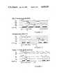
- FIG. 1shows the organization of the MOS imaging device of the invention.
- FIG. 2is a timing diagram of the non-interlace, monochrome mode of operation.
- FIG. 3is a timing diagram of the interlace, monochrome operation.
- FIG. 4is a timing diagram of the pseudo-interlace, monochrome mode of operation.
- FIG. 5is a timing diagram of the non-interlace color mode of operation.
- FIG. 6is a timing diagram of the pseudo-interlace, color mode of operation.
- FIG. 1shows the organization of the MOS imager of the invention.
- a typical pixel elementis represented by the block 10.
- Each pixelis comprised of a PN diode 12 which is exposed to light from a scene and which generates photoelectric pairs of holes and electrons. This charge is stored in the junction capacitance of the diode or some other storage capacitance until it is time to read the signal from the pixel. The amount of charge generated in each pixel depends upon the intensity of the light from the scene falling on that pixel.
- the charge from each pixelis read out by turning on an MOS transistor 14 associated with each diode.
- the MOS transistor 14has its source coupled to the cathode of the diode 12 and has its drain coupled to a column video signal line 16.
- the gate of the MOS transistor 14is coupled to a row address line 18. When the row address line 18 has a predetermined voltage applied thereto exceeding the threshold voltage of the transistor 14, the MOS transistor 14 turns on and the charge stored in the junction capacitance of the diode 12 is coupled through the channel region of the MOS transistor to the column video signal line 16.
- each pixelis conventional and any design and method of making a conventional MOS imager pixel element will suffice for practicing the invention.
- the pixel design taught in the Hitachi paper mentioned abovewill be satisfactory.
- the cells in either of U.S. Pat. Nos. 4,143,389 or 4,155,094will be adequate.
- the layout of the individual pixels on the substrateis comprised of rows of interleaved triangular groups. That is, the pixels 10, 20 and 22 form a triangular group because pixels 10, 22 and 32 coupled to the first address line 18 are offset from the pixels 20, 30 and 34 in the second row coupled to an address line 36.
- the offset of the rowsis such that the pixels coupled to the address line 36 line up with the gaps between the pixels coupled to the address line 18.
- triangular groups of three pixels per groupare formed where each pixel in each group is coupled to a different one of three column video signal lines which run through the group. For example, the pixel 10 is coupled to the video signal line 16 while the pixels 20 and 22 are coupled to the video signal lines 38 and 40 respectively.
- This pixel arrangementcreates the possibility for generating full color video outputs if 3 different color filters are physically placed over the individual pixel elements in each group.
- the video signals on the signal lines 16, 38 and 40then represent the color content signals of a single, composite color pixel comprised of the individual pixels 10, 20 and 22.
- the color filterscan be implemented using any conventional method.
- One known way of providing for a color filteris taught in the paper by Aoki et al cited above.
- There a gelatin layeris deposited over the surface of the substrate after the PN junction diodes and MOS transistors are formed.
- the gelatin layeris then sectionalized using photolithography techniques and each section over a pixel is dyed with an appropriate one of the colors selected.
- the color filtersmay also be discrete filters or "fly eye” filters placed over the pixels.
- Such structures and the methods of fabricating themare known in the art. Eastman Kodak has published several papers in this area.
- the Bayer patentU.S. Pat. No. 3,971,065, teaches use of a filter mosaic overlying a CCD area image sensor to produce an array of rows and columns of color responsive photoelements with every other array position occupied by a green-sensitive element serving to detect luminance.
- Red sensitive "chrominance" elementsalternate with the luminance detecting elements in every other row while blue sensitive chrominance elements alternate with the luminance elements in the remaining, alternate rows.
- the luminance and chrominance signals from pairs of the rowsprovide red, blue and green information with green predominating.
- the Dillon Pat. No. 4,047,203teaches an array wherein every other position of the array of horizontal rows and vertical columns of color responsive pixels is also occupied by a green-sensitive, luminance element.
- the chrominance elements of each rowalternate between red and blue along the row so that a pattern of four successive elements, two of which are luminance elements and two of which are different chrominance elements, repeats along the length of each row with one element of horizontal displacements from row to row.
- MOS transistors 46-51each of which is coupled to the gates of two of the MOS transistors 46-51.
- the MOS transistors 46-51each have their sources and drains coupled between one of the video signal lines 16, 38, 40, 44, 46 and 48 and one of the video output lines 41 or 42.
- the two video signal lines 16 and 38can be coupled to the two video output lines 41 and 42.
- another two of the transistors, e.g., transistors 48 and 49are turned on as a different output from the horizontal shift register 44 is activated. This couples a different two of the video signal lines, e.g., the lines 40 and 44, to the output lines 41 and 42.
- the horizontal shift register 44can be any conventional shift register of either the CCD type with driver circuits, flip-flop variety, inverter chains, dynamic source follower chains, or any other known design where successive outputs can be sequentially activated; however, the CCD type is preferred.
- the structure and operation of shift registersis well known in the art.
- the horizontal shift register 44is a two-phase shift register which shifts a single pulse or charge packet through the register under the influence of two-phased clock signals ⁇ 11 and ⁇ 12 .
- the MOS transistors 46 and 47are turned on thereby coupling the vertical signal lines 16 and 38 to be coupled to the video output lines 41 and 42 respectively.
- the transistors 48 and 49are turned on and the video signal lines 40 and 44 are thereby coupled to the video output lines 41 and 42.
- a second horizontal shift register 56causes coupling between the video signal lines 16, 38, 40, 44, 46 and 48 and three color video output lines 57, 58 and 59.
- the second horizontal shift register 56can be the same structure and operate in the same fashion as the horizontal shift register 44 except that its output lines are each coupled to the gates of three switching transistors instead of only two as in the case of the shift register 44. That is, an output line 60 is coupled to each of the gates of three MOS switching transistors 61-63. When a pulse or charge packet shifts past the output line 60, the three transistors 61-63 all turn on thereby coupling the video signal lines 16, 38 and 40 to the color video output lines 57-59 respectively.
- the output line 64operates in the same manner in conjunction with switching transistors 65-67 and video signal lines 44, 46 and 48.
- the reading of the image arraycan be accomplished in several ways by virtue of the use of two vertical shift registers which are coupled to alternate address lines in the array.
- a vertical shift register 68having the same structure as the horizontal shift registers 44 and 56, has its outputs coupled to every other address line in the array. That is, the outputs from the vertical shift register 68 are the address lines 18 and 69-71. These address lines are coupled to the gates of the MOS switching transistors for the pixels in every other row.
- the even rows address linesare the output lines of a vertical shift register 72.
- the vertical shift register 72has the same structure as the horizontal shift registers 56 and 44 and operates in the same manner.
- the horizontal shift register 44has a similar set of switches 106 and 108 to deactivate it for color operation. With the horizontal shift register 56 deactivated, the switching transistors 61-63 and 65-67 are open circuits and the video output lines 57-59 are therefore deactivated. This leaves only the output lines 41 and 42 activated for monochrome operation.
- Monochrome readoutoccurs in the non-interlaced mode as shown in FIG. 2 and described below.
- the non-interlace modemeans that first an even row is read out and then the next odd row is read out. This even-odd-even-odd read-out continues until the entire array has been read out. In FIG. 2 this sequence of events is shown inferentially by the relationships depicted between the signals shown.
- the ⁇ 41 and ⁇ 42 signalsdrive the vertical shift register 68 in the known manner for two-phase registers.
- the pulses 78 and 80represent the two pulses necessary to move the pulse or charge packet from one register stage to the next.
- the pulses 78 and 80can be thought of as transferring the single pulse or charge packet in the vertical shift register 68 into the first register stage so as to charge the first odd address line 18.
- the signals on the video signal lines 16, 40 and 46must be connected to the black and white video output line 41. This happens sequentially under the influence of the horizontal shift register 44 which is driven by the clock signals ⁇ 11 and ⁇ 12 .
- These clock signalsare represented by the numerous vertical lines within the rectangular region 86 in FIG. 2. These lines represent two clock pulses ⁇ 11 and ⁇ 12 for each output line 52, 54, etc. from the shift register 44.
- the transistor 46turns on and the video signal line 16 is coupled to the video output line 41.
- a video output signalcan then be read from video output line 41 representing the light intensity falling on the pixel consisting of the transistor 14 and the diode 12.
- the horizontal shift register 44turns on the transistor 48 and the transistor 46 will turn off. At that time, the video signal from the pixel comprised of the transistor 82 and the diode 88 is coupled through the video signal line 40 and the transistor 48 to the video output line 41.
- the horizontal shift register 44turns on the transistor 50 and turns off the transistor 48 thereby coupling the pixel comprised of the transistor 84 and the diode 90 to the video output line 41.
- clock pulses 92 and 94occur in the signals ⁇ 31 and ⁇ 32 to activate the next row of pixels.
- a blanking intervaloccurs between the series of clock pulses represented by the blocks 86 and 96 for retrace to the beginning of the next horizontal line by the sweep circuitry in the video equipment used to display the output signals from the invention.
- These pulsesrepresent the first transfer of the single pulse or charge packet in the vertical shift register 72. These two pulses cause the charge packet to be transferred into the register stage in the shift register 72 (not shown) which is associated with the first even address line 36. Thus all the switching transistors connected to the address line 36 are turned on.
- the horizontal shift register 44then sweeps out all the signals from the pixels connected to the address line 36 by turning on in sequence, the transistors 47, 49 and 51 respectively connected to the video signal lines 38, 44 and 48.
- This process of clocking out the signalsis represented by the vertical lines inside the rectangular region 96 in FIG. 2 representing the individual clock pulses ⁇ 11 and ⁇ 12 . This pattern is repeated for all the rows in the array.
- FIG. 3represents the interlaced readout mode for monochrome operation. Again the horizontal shift register 56 is deactivated by the switches 74 and 76. In the interlace mode, first all the odd rows are read out for one field and then all the even rows are read out for the next field. This is indicated in FIG. 3 by the absence of any pulses in the ⁇ 31 and ⁇ 32 signals until the ⁇ 41 and ⁇ 42 clock pulses have activated each of the odd address lines connected to the vertical shift register 68. The first field is read out between the times t 1 and t 2 . The next field readout begins after the time t 2 upon the occurrence of the pulses 98 and 99 in the signals ⁇ 31 and ⁇ 32 .
- FIG. 4represents the pseudo-interlace, monochrome mode of operation.
- the odd and even rowsare read out simultaneously as pairs. This is represented in FIG. 4 by the simultaneous occurrence of the pulses 100 and 102 in the ⁇ 41 and ⁇ 31 signals and the simultaneous occurrence of the pulses 101 and 103 in the ⁇ 42 and ⁇ 32 .
- the simultaneous occurrence of pulses 101 and 103causes the first odd address line 18 and the first even address line 36 to be simultaneously charged so as to turn on all the switching transistors connected to these two rows.
- the ⁇ 11 and ⁇ 12 pulses represented by the vertical lines in the rectangular area 104then sweep the individual pixel signals out on the video output lines 41 and 42.
- the odd pixels connected to the address line 18are swept out on the video output line 41 while the even pixels connected to the address line 36 are simultaneously swept out on the video output line 42.
- FIG. 5is a timing diagram for the non-interlace, color mode of operation.
- the horizontal shift register 44is deactivated by the action of circuitry represented by switches 106 and 108 similar to the circuitry represented by the switches 74 and 76.
- the video output lines 57-59are activated.
- the color modethree pixels are lumped together as one composite pixel and each pixel in the trio generates one of the three primary color signals in the composite video.
- the non-interlace modemeans each row is read out in the sequence odd-even-odd . . . until all rows have been read out.
- the non-interlace, color readoutoccurs by simultaneously activating both the odd and the even row address lines for each row of composite color pixels.
- the vertical lines within the region 118 of the representation of the signals ⁇ 21 and ⁇ 22 in FIG. 5represent the individual pulses from the horizontal shift register 56 which activate the output lines 60 and 64 and the associated switching transistors.
- the pulse which activates the line 60turns on the transistors 61-63 which couples the video signal lines 16, 38 and 40 to the video output lines 57-59 respectively. This process of coupling all the video signal lines in the array to the video output lines 57-59 continues during the duration of the pulses 112 and 116 until all the video signal lines in the array have been coupled in turn to their respective color video output lines 57-59.
- FIG. 6is a timing diagram of the pseudo-interlace mode of color operation for the invention.
- the horizontal shift register 44is deactivated by the action of the circuitry represented by the switches 106 and 108.
- the color output lines 57-59are thus activated and are coupled to trios of the video signal lines in the same manner as described in connection with FIG. 5.
- the difference in operation between FIG. 5 and FIG. 6is that in FIG. 5 during each field both of the row address lines for each row of composite color pixels are simultaneously activated.
- one of the row address activation signalslags the other by one period such that the pairing of pulses is different in every other field. That is, the first field in FIG.
- the second fieldbegins at t 4 .
- the simultaneous occurrence of the pulses 132 and 134 in the signals ⁇ 41 and ⁇ 31 and the simultaneous occurrence of the pulses 136 and 138 in the signals ⁇ 42 and ⁇ 32respectively indicate that in this first field the row address lines 18 and 36 are energized as a pair.
- the simultaneous occurrence of the pulses 140 and 142 in the signals ⁇ 41 and ⁇ 31 and the pulses 144 and 146 in ⁇ 42 and ⁇ 32indicate that for readout of the next row of composite color pixels, the row address lines 69 and 128 are activated simultaneously as a pair.
- the operation of the horizontal shift register 56 in this mode of operationis the same as described with reference to FIG. 5.
- the signals ⁇ 41 , ⁇ 42 , ⁇ 31 and ⁇ 32 driving the vertical shift registers 68 and 72 and the signals ⁇ 11 , ⁇ 12 , ⁇ 21 and ⁇ 22 driving the horizontal shift registers 44 and 56are generated by conventional clock logic 160 in the form of an EPROM.
- the design of this clock logic 160is not critical to the invention and any design which supplies the signals shown in FIGS. 2-6 in the relationships there shown will suffice for purposes of the invention.
- the pattern of signals generated by the clock logic 160 and their relationshipscan be set by any conventional means such as by supplying external signals to the clock logic to set internal latches to define the desired mode. Alternatively this could be done by blowing fuses in the EPROM clock logic 160 during fabrication as with a laser by techniques similar to the techniques used to replace defective circuits in integrated memories by patching in redundant circuits on the die.
Landscapes
- Engineering & Computer Science (AREA)
- Multimedia (AREA)
- Signal Processing (AREA)
- Transforming Light Signals Into Electric Signals (AREA)
- Color Television Image Signal Generators (AREA)
- Solid State Image Pick-Up Elements (AREA)
Abstract
Description
Claims (19)
Priority Applications (4)
| Application Number | Priority Date | Filing Date | Title |
|---|---|---|---|
| US06/584,855US4658287A (en) | 1984-02-29 | 1984-02-29 | MOS imaging device with monochrome-color compatibility and signal readout versatility |
| EP85400246AEP0157660A3 (en) | 1984-02-29 | 1985-02-14 | Mos imaging device with monochrome-color compatibility and signal readout versatility |
| JP60036710AJPS60206169A (en) | 1984-02-29 | 1985-02-27 | MOS image processing device with monochrome/color compatibility and signal reading versatility |
| CA000475359ACA1228667A (en) | 1984-02-29 | 1985-02-28 | Mos imaging device with monochrome-color compatability and signal readout versatility |
Applications Claiming Priority (1)
| Application Number | Priority Date | Filing Date | Title |
|---|---|---|---|
| US06/584,855US4658287A (en) | 1984-02-29 | 1984-02-29 | MOS imaging device with monochrome-color compatibility and signal readout versatility |
Publications (1)
| Publication Number | Publication Date |
|---|---|
| US4658287Atrue US4658287A (en) | 1987-04-14 |
Family
ID=24339061
Family Applications (1)
| Application Number | Title | Priority Date | Filing Date |
|---|---|---|---|
| US06/584,855Expired - LifetimeUS4658287A (en) | 1984-02-29 | 1984-02-29 | MOS imaging device with monochrome-color compatibility and signal readout versatility |
Country Status (4)
| Country | Link |
|---|---|
| US (1) | US4658287A (en) |
| EP (1) | EP0157660A3 (en) |
| JP (1) | JPS60206169A (en) |
| CA (1) | CA1228667A (en) |
Cited By (28)
| Publication number | Priority date | Publication date | Assignee | Title |
|---|---|---|---|---|
| US4709259A (en)* | 1985-05-08 | 1987-11-24 | Fuji Photo Film Co., Ltd. | Color image sensor |
| US4764813A (en)* | 1985-09-20 | 1988-08-16 | Fuji Photo Film Co., Ltd. | Variable order and period solid state image pickup device |
| EP0285894A1 (en)* | 1987-03-31 | 1988-10-12 | Canon Kabushiki Kaisha | Imaging apparatus |
| US4786819A (en)* | 1985-06-18 | 1988-11-22 | Fuji Xerox Co., Ltd. | Method of fabricating a contact type color image sensor |
| US4802001A (en)* | 1985-09-20 | 1989-01-31 | Fuji Photo Film Co., Ltd. | Micro filter arrangement in an interlaced solid-state image pickup element |
| US4959723A (en)* | 1987-11-06 | 1990-09-25 | Canon Kabushiki Kaisha | Solid state image pickup apparatus having multi-phase scanning pulse to read out accumulated signal |
| US5111263A (en)* | 1991-02-08 | 1992-05-05 | Eastman Kodak Company | Charge-coupled device (CCD) image sensor operable in either interlace or non-interlace mode |
| GB2223909B (en)* | 1988-09-06 | 1992-09-23 | Mitsubishi Electric Corp | Apparatus for driving solid-state image pickup device |
| US5172220A (en)* | 1988-07-20 | 1992-12-15 | Geutebruck Videotechnik GmbH | Day-night black and white and color video camera |
| US5241377A (en)* | 1991-01-11 | 1993-08-31 | Mitsubishi Denki Kabushiki Kaisha | Compact imager including a plurality of photodiode arrays |
| US5262850A (en)* | 1988-09-20 | 1993-11-16 | Canon Kabushiki Kaisha | Photoelectric converting device having reduced line sensor space |
| US5495289A (en)* | 1992-07-31 | 1996-02-27 | Sony Corporation | Fit solid state image sensor with flicker suppression |
| EP0710034A2 (en) | 1994-10-31 | 1996-05-01 | Symbios Logic Inc. | Apparatus and method for image scanning using a sensor array |
| EP0812114A4 (en)* | 1995-12-21 | 2001-05-09 | Sony Corp | SEMICONDUCTOR IMAGE DETECTOR, METHOD FOR ACTUATING THE SAME, DEVICE FOR SEMICONDUCTOR CAMERA, AND SEMICONDUCTOR CAMERA |
| US6326997B1 (en)* | 1996-12-30 | 2001-12-04 | Samsung Aerospace Industries, Ltd. | Digital still camera utilizing a progressive image sensor |
| US20020071041A1 (en)* | 2000-12-07 | 2002-06-13 | Pine Joshua I. | Enhanced resolution mode using color image capture device |
| EP0967795A3 (en)* | 1998-06-22 | 2002-07-03 | Eastman Kodak Company | Parallel output architectures for CMOS active pixel sensors |
| US6452632B1 (en) | 1997-01-31 | 2002-09-17 | Kabushiki Kaisha Toshiba | Solid state image sensor and video system using the same |
| US20030193593A1 (en)* | 1996-05-22 | 2003-10-16 | Eastman Kodak Company | X-y addressable CMOS APS with compact pixel pitch |
| US6707496B1 (en)* | 1999-09-15 | 2004-03-16 | Omnivision Technologies, Inc. | CMOS sensor having analog delay line for image processing |
| US6784928B1 (en)* | 1997-12-25 | 2004-08-31 | Canon Kabushiki Kaisha | Solid state image pickup device and signal reading method thereof |
| US20050012836A1 (en)* | 2003-07-15 | 2005-01-20 | Eastman Kodak Company | Image sensor with charge binning and dual channel readout |
| US20050225657A1 (en)* | 2004-04-08 | 2005-10-13 | Canon Kabushiki Kaisha | Image capture apparatus configured to divisionally read out accumulated charges with a plurality of fields using interlaced scanning |
| US20050276369A1 (en)* | 2004-05-20 | 2005-12-15 | Kohei Mutaguchi | Shift register and electronic device using the same |
| US7142233B1 (en)* | 1997-12-26 | 2006-11-28 | Canon Kabushiki Kaishi | Image pickup element |
| US20090086070A1 (en)* | 2007-10-02 | 2009-04-02 | Olympus Corporation | Solid-state imaging apparatus |
| US20100085456A1 (en)* | 2004-05-18 | 2010-04-08 | Olympus Corporation | Solid-state image-pickup sensor and device |
| CN101035191B (en)* | 2006-03-06 | 2013-03-20 | 索尼株式会社 | Solid state image forming device, method of driving the same and camera |
Families Citing this family (4)
| Publication number | Priority date | Publication date | Assignee | Title |
|---|---|---|---|---|
| CA1269446A (en)* | 1984-12-28 | 1990-05-22 | Seiji Hashimoto | Image sensing apparatus |
| JPS61189064A (en)* | 1985-02-18 | 1986-08-22 | Fuji Photo Film Co Ltd | Storage type image sensor |
| JPH03190171A (en)* | 1989-12-12 | 1991-08-20 | Samsung Electron Devices Co Ltd | CCD type solid-state image sensor |
| JP4385844B2 (en)* | 2004-04-23 | 2009-12-16 | ソニー株式会社 | Solid-state imaging device and driving method of solid-state imaging device |
Citations (4)
| Publication number | Priority date | Publication date | Assignee | Title |
|---|---|---|---|---|
| JPS5379430A (en)* | 1976-12-24 | 1978-07-13 | Hitachi Ltd | Color solid state pickup device |
| JPS5597781A (en)* | 1979-01-19 | 1980-07-25 | Matsushita Electric Ind Co Ltd | Color television camera |
| JPS5850881A (en)* | 1981-09-21 | 1983-03-25 | Hitachi Ltd | Imaging device |
| DE3305027A1 (en)* | 1982-02-19 | 1983-09-01 | Thomson-Brandt, 75008 Paris | COLOR TELEVISION CAMERA WITH A THREE-COLOR MATRIX FILTER |
Family Cites Families (1)
| Publication number | Priority date | Publication date | Assignee | Title |
|---|---|---|---|---|
| FR2533056B1 (en)* | 1982-09-14 | 1987-05-15 | Thomson Csf | LINE TRANSFER IMAGER AND TELEVISION CAMERA PROVIDED WITH SUCH AN IMAGER |
- 1984
- 1984-02-29USUS06/584,855patent/US4658287A/ennot_activeExpired - Lifetime
- 1985
- 1985-02-14EPEP85400246Apatent/EP0157660A3/ennot_activeWithdrawn
- 1985-02-27JPJP60036710Apatent/JPS60206169A/enactivePending
- 1985-02-28CACA000475359Apatent/CA1228667A/ennot_activeExpired
Patent Citations (5)
| Publication number | Priority date | Publication date | Assignee | Title |
|---|---|---|---|---|
| JPS5379430A (en)* | 1976-12-24 | 1978-07-13 | Hitachi Ltd | Color solid state pickup device |
| JPS5597781A (en)* | 1979-01-19 | 1980-07-25 | Matsushita Electric Ind Co Ltd | Color television camera |
| JPS5850881A (en)* | 1981-09-21 | 1983-03-25 | Hitachi Ltd | Imaging device |
| DE3305027A1 (en)* | 1982-02-19 | 1983-09-01 | Thomson-Brandt, 75008 Paris | COLOR TELEVISION CAMERA WITH A THREE-COLOR MATRIX FILTER |
| US4553159A (en)* | 1982-02-19 | 1985-11-12 | Thomson-Brandt | Color television camera comprising a trichrome matrix filter |
Cited By (37)
| Publication number | Priority date | Publication date | Assignee | Title |
|---|---|---|---|---|
| US4709259A (en)* | 1985-05-08 | 1987-11-24 | Fuji Photo Film Co., Ltd. | Color image sensor |
| US4786819A (en)* | 1985-06-18 | 1988-11-22 | Fuji Xerox Co., Ltd. | Method of fabricating a contact type color image sensor |
| US4764813A (en)* | 1985-09-20 | 1988-08-16 | Fuji Photo Film Co., Ltd. | Variable order and period solid state image pickup device |
| US4802001A (en)* | 1985-09-20 | 1989-01-31 | Fuji Photo Film Co., Ltd. | Micro filter arrangement in an interlaced solid-state image pickup element |
| EP0285894A1 (en)* | 1987-03-31 | 1988-10-12 | Canon Kabushiki Kaisha | Imaging apparatus |
| US4876601A (en)* | 1987-03-31 | 1989-10-24 | Canon Kabushiki Kaisha | Imaging apparatus having zoom capability via readout variation |
| US4959723A (en)* | 1987-11-06 | 1990-09-25 | Canon Kabushiki Kaisha | Solid state image pickup apparatus having multi-phase scanning pulse to read out accumulated signal |
| US5172220A (en)* | 1988-07-20 | 1992-12-15 | Geutebruck Videotechnik GmbH | Day-night black and white and color video camera |
| GB2223909B (en)* | 1988-09-06 | 1992-09-23 | Mitsubishi Electric Corp | Apparatus for driving solid-state image pickup device |
| US5262850A (en)* | 1988-09-20 | 1993-11-16 | Canon Kabushiki Kaisha | Photoelectric converting device having reduced line sensor space |
| US5241377A (en)* | 1991-01-11 | 1993-08-31 | Mitsubishi Denki Kabushiki Kaisha | Compact imager including a plurality of photodiode arrays |
| US5111263A (en)* | 1991-02-08 | 1992-05-05 | Eastman Kodak Company | Charge-coupled device (CCD) image sensor operable in either interlace or non-interlace mode |
| US5495289A (en)* | 1992-07-31 | 1996-02-27 | Sony Corporation | Fit solid state image sensor with flicker suppression |
| EP0710034A2 (en) | 1994-10-31 | 1996-05-01 | Symbios Logic Inc. | Apparatus and method for image scanning using a sensor array |
| US5521640A (en)* | 1994-10-31 | 1996-05-28 | At&T Global Information Solutions Company | Color image array scanner with high resolution monochrome mode |
| EP0812114A4 (en)* | 1995-12-21 | 2001-05-09 | Sony Corp | SEMICONDUCTOR IMAGE DETECTOR, METHOD FOR ACTUATING THE SAME, DEVICE FOR SEMICONDUCTOR CAMERA, AND SEMICONDUCTOR CAMERA |
| US20030193593A1 (en)* | 1996-05-22 | 2003-10-16 | Eastman Kodak Company | X-y addressable CMOS APS with compact pixel pitch |
| US6326997B1 (en)* | 1996-12-30 | 2001-12-04 | Samsung Aerospace Industries, Ltd. | Digital still camera utilizing a progressive image sensor |
| US7012635B2 (en) | 1997-01-31 | 2006-03-14 | Kabushiki Kaisha Toshiba | Solid state image sensor and video system using the same |
| US6452632B1 (en) | 1997-01-31 | 2002-09-17 | Kabushiki Kaisha Toshiba | Solid state image sensor and video system using the same |
| US20020145669A1 (en)* | 1997-01-31 | 2002-10-10 | Masafumi Umeda | Solid state image sensor and video system using the same |
| USRE44888E1 (en) | 1997-01-31 | 2014-05-13 | Kabushiki Kaisha Toshiba | Solid state image sensor and video system using the same |
| US6784928B1 (en)* | 1997-12-25 | 2004-08-31 | Canon Kabushiki Kaisha | Solid state image pickup device and signal reading method thereof |
| US7142233B1 (en)* | 1997-12-26 | 2006-11-28 | Canon Kabushiki Kaishi | Image pickup element |
| EP0967795A3 (en)* | 1998-06-22 | 2002-07-03 | Eastman Kodak Company | Parallel output architectures for CMOS active pixel sensors |
| US6707496B1 (en)* | 1999-09-15 | 2004-03-16 | Omnivision Technologies, Inc. | CMOS sensor having analog delay line for image processing |
| US20020071041A1 (en)* | 2000-12-07 | 2002-06-13 | Pine Joshua I. | Enhanced resolution mode using color image capture device |
| US7859581B2 (en)* | 2003-07-15 | 2010-12-28 | Eastman Kodak Company | Image sensor with charge binning and dual channel readout |
| US20050012836A1 (en)* | 2003-07-15 | 2005-01-20 | Eastman Kodak Company | Image sensor with charge binning and dual channel readout |
| US20050225657A1 (en)* | 2004-04-08 | 2005-10-13 | Canon Kabushiki Kaisha | Image capture apparatus configured to divisionally read out accumulated charges with a plurality of fields using interlaced scanning |
| US7616354B2 (en)* | 2004-04-08 | 2009-11-10 | Canon Kabushiki Kaisha | Image capture apparatus configured to divisionally read out accumulated charges with a plurality of fields using interlaced scanning |
| US20100085456A1 (en)* | 2004-05-18 | 2010-04-08 | Olympus Corporation | Solid-state image-pickup sensor and device |
| US20050276369A1 (en)* | 2004-05-20 | 2005-12-15 | Kohei Mutaguchi | Shift register and electronic device using the same |
| US7245690B2 (en) | 2004-05-20 | 2007-07-17 | Semiconductor Energy Laboratory Co., Ltd. | Shift register and electronic device using the same |
| CN101035191B (en)* | 2006-03-06 | 2013-03-20 | 索尼株式会社 | Solid state image forming device, method of driving the same and camera |
| US20090086070A1 (en)* | 2007-10-02 | 2009-04-02 | Olympus Corporation | Solid-state imaging apparatus |
| US8164664B2 (en)* | 2007-10-02 | 2012-04-24 | Olympus Corporation | Solid-state imaging apparatus having a reduced number of wirings within a pixel section |
Also Published As
| Publication number | Publication date |
|---|---|
| JPS60206169A (en) | 1985-10-17 |
| CA1228667A (en) | 1987-10-27 |
| EP0157660A2 (en) | 1985-10-09 |
| EP0157660A3 (en) | 1987-12-02 |
Similar Documents
| Publication | Publication Date | Title |
|---|---|---|
| US4658287A (en) | MOS imaging device with monochrome-color compatibility and signal readout versatility | |
| US5705837A (en) | Solid-state image pick-up device of the charge-coupled device type synchronizing drive signals for a full-frame read-out | |
| US6452634B1 (en) | Charge transfer device and method of driving the same, and solid state imaging device and method of driving the same | |
| US4816916A (en) | CCD area image sensor operable in both of line-sequential and interlace scannings and a method for operating the same | |
| US4277799A (en) | Color solid-state imaging device | |
| US4349743A (en) | Solid-state imaging device | |
| US6496224B2 (en) | Imaging device including thinned read out mode and all pixel read out mode | |
| US7218348B2 (en) | Solid-state electronic imaging device and method of controlling opertion thereof | |
| JPS5984575A (en) | Solid-state image-pickup element | |
| US5239380A (en) | Method of driving a solid-state imaging device by two-step signal charge vertical transfer in one horizontal blanking period | |
| US4322740A (en) | Solid-state color imaging camera | |
| US7379107B2 (en) | Image sensor for still or video photography | |
| KR0186201B1 (en) | Color linear CD image device and driving method thereof | |
| US4675887A (en) | Solid state imaging device and method with row-by-row charge transfer | |
| US4862487A (en) | Solid-state imaging device | |
| US8045025B2 (en) | Image pickup device adaptable to display fewer vertical pixels | |
| GB2261113A (en) | Solid-state image sensor | |
| US4532549A (en) | Solid-state imaging device with high quasi-signal sweep-out efficiency and high signal charge transfer efficiency | |
| JPS60134675A (en) | Solid-state imaging device and its manufacturing method | |
| JPH0533594B2 (en) | ||
| JP3367852B2 (en) | Solid-state imaging device | |
| JP2658443B2 (en) | Driving method of solid-state imaging device | |
| US5978026A (en) | Solid-state image pickup device | |
| JPS5814789B2 (en) | Color Kotai Satsuzou Sochi | |
| JP2880011B2 (en) | Solid-state imaging device |
Legal Events
| Date | Code | Title | Description |
|---|---|---|---|
| AS | Assignment | Owner name:FAIRCHILD CAMERA AND INSTRUMENT CORPORATION, 464 E Free format text:ASSIGNMENT OF ASSIGNORS INTEREST.;ASSIGNOR:CHEN, CHENG-WEI;REEL/FRAME:004237/0249 Effective date:19840224 | |
| STCF | Information on status: patent grant | Free format text:PATENTED CASE | |
| FEPP | Fee payment procedure | Free format text:PAYOR NUMBER ASSIGNED (ORIGINAL EVENT CODE: ASPN); ENTITY STATUS OF PATENT OWNER: LARGE ENTITY | |
| FPAY | Fee payment | Year of fee payment:4 | |
| FPAY | Fee payment | Year of fee payment:8 | |
| AS | Assignment | Owner name:NATIONAL SEMICONDUCTOR CORPORATION, CALIFORNIA Free format text:ASSIGNMENT OF ASSIGNORS INTEREST;ASSIGNOR:FAIRCHILD SEMICONDUCTOR CORPORATION;REEL/FRAME:008059/0846 Effective date:19960726 | |
| FEPP | Fee payment procedure | Free format text:PAYER NUMBER DE-ASSIGNED (ORIGINAL EVENT CODE: RMPN); ENTITY STATUS OF PATENT OWNER: LARGE ENTITY Free format text:PAYOR NUMBER ASSIGNED (ORIGINAL EVENT CODE: ASPN); ENTITY STATUS OF PATENT OWNER: LARGE ENTITY | |
| FPAY | Fee payment | Year of fee payment:12 | |
| AS | Assignment | Owner name:FAIRCHILD SEMICONDUCTOR CORPORATION, NEW YORK Free format text:CHANGE OF NAME;ASSIGNOR:FAIRCHILD CAMERA AND INSTRUMENT CORPORATION, A DELAWARE CORPORATION;REEL/FRAME:011692/0679 Effective date:19851015 | |
| AS | Assignment | Owner name:FAIRCHILD WESTON SYSTEMS, INC., NEW YORK Free format text:ASSIGNMENT OF ASSIGNORS INTEREST;ASSIGNOR:FAICHILD SEMICONDUCTOR CORPORATION, A CORP. OF DE;REEL/FRAME:011712/0169 Effective date:19870914 | |
| AS | Assignment | Owner name:LORAL COMPUTER SYSTEMS CORPORATION, NEW YORK Free format text:ASSIGNMENT OF ASSIGNORS INTEREST;ASSIGNORS:SANGAMO WESTON, INC.;SCHULUMBERGER TECHNOLOGY CORPORATION;SCHLUMBERGER INDUSTRIES LIMITED;AND OTHERS;REEL/FRAME:011763/0740 Effective date:19890627 Owner name:CLOSERAY LIMITED, NEW YORK Free format text:ASSIGNMENT OF ASSIGNORS INTEREST;ASSIGNORS:SANGAMO WESTON, INC.;SCHULUMBERGER TECHNOLOGY CORPORATION;SCHLUMBERGER INDUSTRIES LIMITED;AND OTHERS;REEL/FRAME:011763/0740 Effective date:19890627 | |
| AS | Assignment | Owner name:LORAL FAIRCHILD CORPORATION, NEW YORK Free format text:CHANGE OF NAME;ASSIGNOR:LORAL COMPUTER SYSTEMS CORPORATION;REEL/FRAME:011783/0792 Effective date:19890706 | |
| AS | Assignment | Owner name:LOCKHEED MARTIN FAIRCHILD CORPORATION, A CORP. OF Free format text:CHANGE OF NAME;ASSIGNOR:LORAL FAIRCHILD CORPORATION, A CORP. OF DELAWARE;REEL/FRAME:011796/0337 Effective date:19960429 | |
| AS | Assignment | Owner name:LOCKHEED MARTIN CORPORATION, MARYLAND Free format text:MERGER;ASSIGNOR:LOCKHEED MARTIN FAIRCHILD CORPORATION, A DELAWARE CORPORATION;REEL/FRAME:011898/0249 Effective date:19970627 | |
| AS | Assignment | Owner name:BAE SYSTEMS INFORMATION AND ELECTRONIC SYSTEMS INT Free format text:ASSIGNMENT OF ASSIGNORS INTEREST;ASSIGNOR:LOCKHEED MARTIN CORPORATION;REEL/FRAME:011862/0904 Effective date:20001127 |