US4655554A - Spatial light modulator having a capacitively coupled photoconductor - Google Patents
Spatial light modulator having a capacitively coupled photoconductorDownload PDFInfo
- Publication number
- US4655554A US4655554AUS06/708,926US70892685AUS4655554AUS 4655554 AUS4655554 AUS 4655554AUS 70892685 AUS70892685 AUS 70892685AUS 4655554 AUS4655554 AUS 4655554A
- Authority
- US
- United States
- Prior art keywords
- spatial light
- light modulator
- electro
- optic crystal
- silicon
- Prior art date
- Legal status (The legal status is an assumption and is not a legal conclusion. Google has not performed a legal analysis and makes no representation as to the accuracy of the status listed.)
- Expired - Fee Related
Links
- 239000004065semiconductorSubstances0.000claimsabstractdescription15
- 239000013078crystalSubstances0.000claimsdescription28
- 229910052710siliconInorganic materials0.000claimsdescription22
- 239000010703siliconSubstances0.000claimsdescription22
- 239000000758substrateSubstances0.000claimsdescription21
- VYPSYNLAJGMNEJ-UHFFFAOYSA-NSilicium dioxideChemical compoundO=[Si]=OVYPSYNLAJGMNEJ-UHFFFAOYSA-N0.000claimsdescription8
- 239000004973liquid crystal related substanceSubstances0.000claimsdescription7
- 239000000463materialSubstances0.000claimsdescription6
- 239000000377silicon dioxideSubstances0.000claimsdescription4
- 235000012239silicon dioxideNutrition0.000claimsdescription4
- GQYHUHYESMUTHG-UHFFFAOYSA-Nlithium niobateChemical compound[Li+].[O-][Nb](=O)=OGQYHUHYESMUTHG-UHFFFAOYSA-N0.000claimsdescription2
- 108091008695photoreceptorsProteins0.000abstract1
- SBEQWOXEGHQIMW-UHFFFAOYSA-NsiliconChemical class[Si].[Si]SBEQWOXEGHQIMW-UHFFFAOYSA-N0.000abstract1
- XUIMIQQOPSSXEZ-UHFFFAOYSA-NSiliconChemical compound[Si]XUIMIQQOPSSXEZ-UHFFFAOYSA-N0.000description21
- 238000005286illuminationMethods0.000description8
- 230000003287optical effectEffects0.000description7
- 230000000903blocking effectEffects0.000description6
- 238000010276constructionMethods0.000description3
- JBRZTFJDHDCESZ-UHFFFAOYSA-NAsGaChemical compound[As]#[Ga]JBRZTFJDHDCESZ-UHFFFAOYSA-N0.000description2
- 229910001218Gallium arsenideInorganic materials0.000description2
- 239000000969carrierSubstances0.000description2
- 230000015556catabolic processEffects0.000description2
- 239000002131composite materialSubstances0.000description2
- 230000008878couplingEffects0.000description2
- 238000010168coupling processMethods0.000description2
- 238000005859coupling reactionMethods0.000description2
- 238000010586diagramMethods0.000description2
- 230000005684electric fieldEffects0.000description2
- 238000002955isolationMethods0.000description2
- 239000002210silicon-based materialSubstances0.000description2
- WSMQKESQZFQMFW-UHFFFAOYSA-N5-methyl-pyrazole-3-carboxylic acidChemical compoundCC1=CC(C(O)=O)=NN1WSMQKESQZFQMFW-UHFFFAOYSA-N0.000description1
- KRHYYFGTRYWZRS-UHFFFAOYSA-MFluoride anionChemical compound[F-]KRHYYFGTRYWZRS-UHFFFAOYSA-M0.000description1
- 229910003327LiNbO3Inorganic materials0.000description1
- 229910012463LiTaO3Inorganic materials0.000description1
- 230000002411adverseEffects0.000description1
- 239000002800charge carrierSubstances0.000description1
- 230000007423decreaseEffects0.000description1
- 230000000593degrading effectEffects0.000description1
- 238000000151depositionMethods0.000description1
- 238000001514detection methodMethods0.000description1
- 230000000694effectsEffects0.000description1
- PCHJSUWPFVWCPO-UHFFFAOYSA-NgoldChemical compound[Au]PCHJSUWPFVWCPO-UHFFFAOYSA-N0.000description1
- 239000010931goldSubstances0.000description1
- 229910052737goldInorganic materials0.000description1
- 238000003384imaging methodMethods0.000description1
- 238000004519manufacturing processMethods0.000description1
- 229920006254polymer filmPolymers0.000description1
- GNSKLFRGEWLPPA-ZSJDYOACSA-Mpotassium;dideuterio phosphateChemical compound[K+].[2H]OP([O-])(=O)O[2H]GNSKLFRGEWLPPA-ZSJDYOACSA-M0.000description1
Images
Classifications
- G—PHYSICS
- G02—OPTICS
- G02F—OPTICAL DEVICES OR ARRANGEMENTS FOR THE CONTROL OF LIGHT BY MODIFICATION OF THE OPTICAL PROPERTIES OF THE MEDIA OF THE ELEMENTS INVOLVED THEREIN; NON-LINEAR OPTICS; FREQUENCY-CHANGING OF LIGHT; OPTICAL LOGIC ELEMENTS; OPTICAL ANALOGUE/DIGITAL CONVERTERS
- G02F1/00—Devices or arrangements for the control of the intensity, colour, phase, polarisation or direction of light arriving from an independent light source, e.g. switching, gating or modulating; Non-linear optics
- G02F1/01—Devices or arrangements for the control of the intensity, colour, phase, polarisation or direction of light arriving from an independent light source, e.g. switching, gating or modulating; Non-linear optics for the control of the intensity, phase, polarisation or colour
- G02F1/13—Devices or arrangements for the control of the intensity, colour, phase, polarisation or direction of light arriving from an independent light source, e.g. switching, gating or modulating; Non-linear optics for the control of the intensity, phase, polarisation or colour based on liquid crystals, e.g. single liquid crystal display cells
- G02F1/133—Constructional arrangements; Operation of liquid crystal cells; Circuit arrangements
- G02F1/135—Liquid crystal cells structurally associated with a photoconducting or a ferro-electric layer, the properties of which can be optically or electrically varied
- G—PHYSICS
- G02—OPTICS
- G02F—OPTICAL DEVICES OR ARRANGEMENTS FOR THE CONTROL OF LIGHT BY MODIFICATION OF THE OPTICAL PROPERTIES OF THE MEDIA OF THE ELEMENTS INVOLVED THEREIN; NON-LINEAR OPTICS; FREQUENCY-CHANGING OF LIGHT; OPTICAL LOGIC ELEMENTS; OPTICAL ANALOGUE/DIGITAL CONVERTERS
- G02F1/00—Devices or arrangements for the control of the intensity, colour, phase, polarisation or direction of light arriving from an independent light source, e.g. switching, gating or modulating; Non-linear optics
- G02F1/01—Devices or arrangements for the control of the intensity, colour, phase, polarisation or direction of light arriving from an independent light source, e.g. switching, gating or modulating; Non-linear optics for the control of the intensity, phase, polarisation or colour
- G02F1/03—Devices or arrangements for the control of the intensity, colour, phase, polarisation or direction of light arriving from an independent light source, e.g. switching, gating or modulating; Non-linear optics for the control of the intensity, phase, polarisation or colour based on ceramics or electro-optical crystals, e.g. exhibiting Pockels effect or Kerr effect
- G02F1/0338—Devices or arrangements for the control of the intensity, colour, phase, polarisation or direction of light arriving from an independent light source, e.g. switching, gating or modulating; Non-linear optics for the control of the intensity, phase, polarisation or colour based on ceramics or electro-optical crystals, e.g. exhibiting Pockels effect or Kerr effect structurally associated with a photoconductive layer or having photo-refractive properties
Definitions
- the present inventionrelates generally to the field of optical signal processing apparatus, and more specifically to a spatial light modulator of simplified construction and improved performance.
- Two-dimensional spatial light modulatorsare devices which allow control of an optical wavefront for processing or imaging operations. These devices, often referred to as light valves in the literature, have potential for application in large screen display systems as well as in optical data processing systems, including missile guidance and robotic vision systems. Listed below are several articles which describe the construction and/or operation of various embodiments of spatial light modulators.
- One basic form of spatial light modulatorcomprises a photosensitive semiconductor substrate or wafer, a light blocking layer, a dielectric mirror and an electro-optic crystal (which may in some applications be a liquid crystal), arranged in a sandwich-like composite structure, and having a voltage applied thereacross.
- the photosensitive semiconductor substrateis often a photodiode formed by depositing p-type silicon material on the silicon substrate and applying a reverse biasing potential thereacross.
- a control (write) illuminationimpinges on the face of the photodiode while an output (read) illumination makes a double pass through the electro-optic crystal.
- the photodioderesponds to intensity variations in the control illumination impinging thereon.
- the write beamexcites carriers in the silicon, which are driven by the internal field to the Si/electro-optic crystal interface.
- the voltage across the silicondecreases, while the voltage across the electro-optic crystal increases.
- the read illuminationpasses through the electro-optic crystal, is reflected off of the dielectric mirror, and again passes through the electro-optic crystal before emerging from the device. Since the diffraction efficiency of the electro-optic crystal is a function of the voltage applied thereacross, (which is a function of the intensity of the write illumination), optical control of the output (read) illumination is achieved.
- photodiodesin high resistance silicon, (or other semiconductors, e.g. gallium arsenide), is a difficult art. Such photodiodes must exhibit a high voltage breakdown characteristic and have low leakage current. Leakage currents are known to occur at the semiconductor edges which adversely affect the overall performance of the spatial light modulator.
- the photodiode junctionis replaced by a capacitively coupled electrode.
- the capacitive couplingis made large compared with the capacitive load of the electro-optic crystal and the other associated series capacitances.
- An applied voltage pulsedepletes the silicon wafer and the voltage is mainly dropped across the silicon wafer.
- a write lightexcites carriers in the silicon wafer and charge transfer raises the voltage across the electro-optic crystal in accordance with the intensity distribution in the write light image.
- the read lightis modulated by the electro-optic response to the crystal charge. Erasure follows the end of the voltage pulse. This is generally accomplished by shorting the voltage input terminals and permitting the device to discharge to equilibrium.
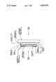
- FIG. 1is a diagram of a spatial light modulator constructed in accordance with a specific embodiment of the invention.
- FIG. 1is a diagram depicting the side view of the spatial light modulator of the present invention.
- the various components thereofhave not been drawn to scale in view of the large differences in their thicknesses. Representative thickness values are provided herein to facilitate an understanding of the invention.
- the spatial light modulatorhas a substrate 10 formed of silicon material having a thickness in the order of 100 microns.
- a transparent dielectric layer 11 of silicon dioxide approximately 0.3 microns thickis formed on one surface of substrate 10 and a transparent electrode 12 of gold approximately 100 angstroms thick is deposited on the dielectric layer 11.
- the other surface of silicon substrate 10is adjacent a layer of light blocking material 14, having a thickness in the order of one micron. (In certain applications, light blocking layer 14 may be unnecessary.)
- Light blocking layer 14is affixed to a dielectric mirror 16 and it, in turn, is affixed to an electro-optic crystal 18 having a thickness in the order of 100 microns.
- the dielectric mirror 16transmits about 0.1% of the read illumination to the silicon substrate 10. In some applications this is not critical. If it is, further isolation is provided by the inclusion of the absorbing or light blocking layer 14 having a thickness less than 10 microns to avoid degrading the resolution of the device. The conductivity of the layer must be low to avoid charge confinement leakage.
- Electro-optic crystal 18is affixed to a transparent electrode 20 having a thickness of approximately 0.25 microns and formed on one surface of a transparent supporting substrate 24 having a thickness in the order of 15 millimeters.
- Transparent electrode 20provides a uniform initial electric field across electro-optic crystal 18.
- a first electrical terminal 26is connected to the transparent electrode 20 and a second electrical terminal 28 is connected to the transparent electrode 12 which, as previously mentioned, is capacitively coupled to the silicon substrate 10.
- a voltage pulse Vis applied across the terminals 26 and 28.
- electro-optic crystal 18be formed of lithium niobate, lithium tantalate or potassium dideuterium phosphate. Electro-optic crystal 18 may also be a liquid crystal device, as proposed in several of the references listed herein.
- the transparent supporting substrate 24may be formed of calcuim fluoride. Lateral charge transfer is inhibited and charge is confined to small areas on the substrate 10 by a p-n junction lattice or a microgroove lattice structure which is demarked by the reference numeral 32.
- the operation of the spatial light modulator shown in FIG. 1is the same as disclosed earlier.
- the control illuminationwhich could in some applications be the fringe pattern of an input hologram, excites electrons and holes in the silicon substrate 10. Electrons are driven by the electric field formed by the voltage pulse V to the silicon substrate 10/electro-optic crystal 18 interface. The silicon depletes; however more electrons and holes are thermally generated which results in a leakage current substantially equal to the bulk generated leakage current that would flow in a diode of the same material and geometry. The edge leakage and microplasm effects associated with a photodiode structure, however, are avoided herein.
- This surface charge pattern in the silicon substrate 10gives rise to a transversely varying voltage pattern containing the same information as the charge pattern. Lateral charge transfer at the crystal 18 side of the semiconductor 10 is inhibited by a p-n junction lattice structure 32, as described in several of the references listed herein, or by a microgroove lattice structure as disclosed by applicant in his copending patent application entitled "Charge Isolation in a Spatial Light Modulator".
- the voltage patternmodulates the index of refraction of the electro-optic crystal 18. The index variations are sensed with the read beam which reconstructs the hologram.
- the dielectric mirror 16is necessary for the read operation and prevents the read beam from destroying the charge pattern at the surface of silicon substrate 10 by creating more charge carriers in the silicon.
- the transparent electrode 20 in conjunction with the applied voltage V,provides a uniform initial field across the electro-optic crystal 18. When the read operation has been completed, the voltage V may be removed from across the terminals 26 and 28, and the input terminals shorted whereby the transversely varied charge pattern will discharge to equilibrium.
- the erasure durationis approximately the carrier lifetime, which is less than a millsecond in silicon.
- the capacitance of the dielectric layer 11 coupling the electrode 12 to the semiconductor 10be large compared with the combined series capacitance of electro-optic crystal 18, dielectric mirror 16, light block 14 and any bonding layers that might be used. If the capacitance of the dielectric layer 11 is identified as C 1 , the capacitance of the silicon wafer 10 as C 2 , the capacitance of the dielectric mirror 16 as C 3 , and the capacitance of the electro-optic crystal 18 as C 4 , then the voltage V c across the crystal 18 is: ##EQU1## By design: C 1 and C 3 >>C 4
- Equation (1)becomes: ##EQU2## with no write light: ##EQU3## with maximum write light: V c ⁇ V
Landscapes
- Physics & Mathematics (AREA)
- Nonlinear Science (AREA)
- Chemical & Material Sciences (AREA)
- Crystallography & Structural Chemistry (AREA)
- General Physics & Mathematics (AREA)
- Optics & Photonics (AREA)
- Mathematical Physics (AREA)
- Engineering & Computer Science (AREA)
- Ceramic Engineering (AREA)
- Optical Modulation, Optical Deflection, Nonlinear Optics, Optical Demodulation, Optical Logic Elements (AREA)
Abstract
Description
The invention described herein may be manufactured and used by or for the Government for governmental purposes without the payment of any royalty thereon.
The present invention relates generally to the field of optical signal processing apparatus, and more specifically to a spatial light modulator of simplified construction and improved performance.
Two-dimensional spatial light modulators are devices which allow control of an optical wavefront for processing or imaging operations. These devices, often referred to as light valves in the literature, have potential for application in large screen display systems as well as in optical data processing systems, including missile guidance and robotic vision systems. Listed below are several articles which describe the construction and/or operation of various embodiments of spatial light modulators.
1. "A Fast Silicon Photoconductor-Based Liquid Crystal Light Valve", P. O. Braatz, K. Chow, U. Efron, J. Grinberg and M. J. Little, IEEE International Electron Devices Meeting, pp 540-543, 1979.
2. "Oblique-cut LiNb O3 Microchannel Spatial Light Modulator", C. Warde and J. I. Thakara, Optics Letters, Vol. 7, No. 7, July 1982.
3. "A First-Order Model of a Photo-Activated Liquid Crystal Light Valve", J. D. Michaelson, SPIE Vol. 218, Devices and Systems For Optical Signal Processing, 1980.
4. "LiNbO3 and LiTaO3 Microchannel Spatial Light Modulators", C. Warde, A. M. Weiss and A. D. Fisher, SPIE Vol. 218, Devices and Systems for Optical Signal Processing, 1980.
5. "Silicon Liquid Crystal Light Valves: Status and Issues", U. Efron, P. O. Braatz, M. J. Little, R. N. Schwartz and J. Grinberg, Proc. SPIE Vol. 388, Jan. 1983.
6. "Spatial modulation of light in a photosensitive structure composed of a liquid crystal and an insulated gallium arsenide crystal", I. N. Kompanets, A. V. Parfenov and Y. M. Popov, Sov. J. Quantum Electron. 9(8) Aug. 1979, pp 1070-1071.
One basic form of spatial light modulator comprises a photosensitive semiconductor substrate or wafer, a light blocking layer, a dielectric mirror and an electro-optic crystal (which may in some applications be a liquid crystal), arranged in a sandwich-like composite structure, and having a voltage applied thereacross. The photosensitive semiconductor substrate is often a photodiode formed by depositing p-type silicon material on the silicon substrate and applying a reverse biasing potential thereacross. A control (write) illumination impinges on the face of the photodiode while an output (read) illumination makes a double pass through the electro-optic crystal.
The photodiode responds to intensity variations in the control illumination impinging thereon. In the dark, most of the voltage applied across the composite structure appears across the reverse-biased photodiode. The write beam, however, excites carriers in the silicon, which are driven by the internal field to the Si/electro-optic crystal interface. The voltage across the silicon decreases, while the voltage across the electro-optic crystal increases. The read illumination passes through the electro-optic crystal, is reflected off of the dielectric mirror, and again passes through the electro-optic crystal before emerging from the device. Since the diffraction efficiency of the electro-optic crystal is a function of the voltage applied thereacross, (which is a function of the intensity of the write illumination), optical control of the output (read) illumination is achieved.
The fabrication of suitable photodiodes in high resistance silicon, (or other semiconductors, e.g. gallium arsenide), is a difficult art. Such photodiodes must exhibit a high voltage breakdown characteristic and have low leakage current. Leakage currents are known to occur at the semiconductor edges which adversely affect the overall performance of the spatial light modulator.
It is therefore the general object of the present invention to provide a spatial light modulator of improved construction and performance.
It is a further object of the present invention to provide a novel and cost effective means for eliminating the leakage and breakdown problems associated with photodiode elements in spatial light modulators.
Briefly, in the spatial light modulator device of the present invention, the photodiode junction is replaced by a capacitively coupled electrode. The capacitive coupling is made large compared with the capacitive load of the electro-optic crystal and the other associated series capacitances. An applied voltage pulse depletes the silicon wafer and the voltage is mainly dropped across the silicon wafer. A write light excites carriers in the silicon wafer and charge transfer raises the voltage across the electro-optic crystal in accordance with the intensity distribution in the write light image. The read light is modulated by the electro-optic response to the crystal charge. Erasure follows the end of the voltage pulse. This is generally accomplished by shorting the voltage input terminals and permitting the device to discharge to equilibrium.
This invention together with its objects, features and advantages may be better understood from the following detailed description when read in conjunction with the drawing, in which:
FIG. 1 is a diagram of a spatial light modulator constructed in accordance with a specific embodiment of the invention.
FIG. 1 is a diagram depicting the side view of the spatial light modulator of the present invention. The various components thereof have not been drawn to scale in view of the large differences in their thicknesses. Representative thickness values are provided herein to facilitate an understanding of the invention.
The spatial light modulator has a substrate 10 formed of silicon material having a thickness in the order of 100 microns. A transparent dielectric layer 11 of silicon dioxide approximately 0.3 microns thick is formed on one surface of substrate 10 and a transparent electrode 12 of gold approximately 100 angstroms thick is deposited on the dielectric layer 11. The other surface of silicon substrate 10 is adjacent a layer oflight blocking material 14, having a thickness in the order of one micron. (In certain applications,light blocking layer 14 may be unnecessary.)Light blocking layer 14 is affixed to adielectric mirror 16 and it, in turn, is affixed to an electro-optic crystal 18 having a thickness in the order of 100 microns.
Thedielectric mirror 16 transmits about 0.1% of the read illumination to the silicon substrate 10. In some applications this is not critical. If it is, further isolation is provided by the inclusion of the absorbing orlight blocking layer 14 having a thickness less than 10 microns to avoid degrading the resolution of the device. The conductivity of the layer must be low to avoid charge confinement leakage.
Electro-optic crystal 18 is affixed to atransparent electrode 20 having a thickness of approximately 0.25 microns and formed on one surface of a transparent supportingsubstrate 24 having a thickness in the order of 15 millimeters.Transparent electrode 20 provides a uniform initial electric field across electro-optic crystal 18. A firstelectrical terminal 26 is connected to thetransparent electrode 20 and a secondelectrical terminal 28 is connected to the transparent electrode 12 which, as previously mentioned, is capacitively coupled to the silicon substrate 10. A voltage pulse V is applied across theterminals
Optical quality and voltage requirements would suggest that electro-optic crystal 18 be formed of lithium niobate, lithium tantalate or potassium dideuterium phosphate. Electro-optic crystal 18 may also be a liquid crystal device, as proposed in several of the references listed herein. The transparent supportingsubstrate 24 may be formed of calcuim fluoride. Lateral charge transfer is inhibited and charge is confined to small areas on the substrate 10 by a p-n junction lattice or a microgroove lattice structure which is demarked by the reference numeral 32.
The operation of the spatial light modulator shown in FIG. 1 is the same as disclosed earlier. The control illumination, which could in some applications be the fringe pattern of an input hologram, excites electrons and holes in the silicon substrate 10. Electrons are driven by the electric field formed by the voltage pulse V to the silicon substrate 10/electro-optic crystal 18 interface. The silicon depletes; however more electrons and holes are thermally generated which results in a leakage current substantially equal to the bulk generated leakage current that would flow in a diode of the same material and geometry. The edge leakage and microplasm effects associated with a photodiode structure, however, are avoided herein. (Since thelight blocking layer 14 anddielectric mirror 16 are thin and of high resistivity, they can be ignored in this analysis.) This surface charge pattern in the silicon substrate 10 gives rise to a transversely varying voltage pattern containing the same information as the charge pattern. Lateral charge transfer at the crystal 18 side of the semiconductor 10 is inhibited by a p-n junction lattice structure 32, as described in several of the references listed herein, or by a microgroove lattice structure as disclosed by applicant in his copending patent application entitled "Charge Isolation in a Spatial Light Modulator". The voltage pattern modulates the index of refraction of the electro-optic crystal 18. The index variations are sensed with the read beam which reconstructs the hologram.
Thedielectric mirror 16 is necessary for the read operation and prevents the read beam from destroying the charge pattern at the surface of silicon substrate 10 by creating more charge carriers in the silicon. The light-blockinglayer 14, if used, attenuates any read beam leakage through thedielectric mirror 16. Thetransparent electrode 20 in conjunction with the applied voltage V, provides a uniform initial field across the electro-optic crystal 18. When the read operation has been completed, the voltage V may be removed from across theterminals
For effective replacement of the photodiode, it is required that the capacitance of the dielectric layer 11 coupling the electrode 12 to the semiconductor 10 be large compared with the combined series capacitance of electro-optic crystal 18,dielectric mirror 16,light block 14 and any bonding layers that might be used. If the capacitance of the dielectric layer 11 is identified as C1, the capacitance of the silicon wafer 10 as C2, the capacitance of thedielectric mirror 16 as C3, and the capacitance of the electro-optic crystal 18 as C4, then the voltage Vc across the crystal 18 is: ##EQU1## By design: C1 and C3 >>C4
Also:
C2 <<C4
Then equation (1) becomes: ##EQU2## with no write light: ##EQU3## with maximum write light: Vc →V
since C2 is shorted by the photocurrent.
Although the invention has been described with reference to a particular embodiment, it will be understood to those skilled in the art that the invention is capable of a variety of alternative embodiments within the spirit and scope of the appended claims. For example, other semiconductor materials may be preferred to silicon, as in applications involving infrared detection. In this application, insulating silicon dioxide could be deposited or a polymer film formed on the semiconductor material.
Claims (7)
1. A spatial light modulator comprising:
a semiconductor element comprising a semiconductor substrate having a first surface and an opposed second surface, a first transparent metallic electrode, a dielectric layer disposed between said first surface of said semiconductor substrate and a surface of said first transparent metallic electrode, and a charge-confining microgroove lattice structure formed in said second surface of said semiconductor substrate;
a dielectric mirror having a first surface and an opposed second surface, said first surface of said dielectric mirror being adjacent said second surface of said semiconductor substrate;
an electro-optic crystal having a first surface and an opposed second surface, said first surface of said electro-optic crystal being adjacent said second surface of said dielectric mirror;
a second transparent electrode having a first surface and an opposed second surface, said first surface of said second transparent electrode being adjacent said second surface of said electro-optic crystal; and
means for applying a voltage pulse between said first transparent electrode and said second transparent electrode.
2. A spatial light modulator as defined in claim 1 and further comprising:
a transparent supporting substrate adjacent said second surface of said second transparent electrode.
3. A spatial light modulator as defined in claim 1 wherein said electro-optic crystal is formed of lithium niobate material.
4. A spatial light modulator as defined in claim 1 wherein said electro-optic crystal is formed of liquid crystal material.
5. A spatial light modulator as defined in claim 1 wherein said semiconductor substrate is formed of silicon.
6. A spatial light modulator as defined in claim 5 wherein said dielectric layer is formed of silicon dioxide.
7. A spatial light modulator as defined in claim 6 wherein said silicon dioxide layer has a thickness of approximately 0.3 microns.
Priority Applications (1)
| Application Number | Priority Date | Filing Date | Title |
|---|---|---|---|
| US06/708,926US4655554A (en) | 1985-03-06 | 1985-03-06 | Spatial light modulator having a capacitively coupled photoconductor |
Applications Claiming Priority (1)
| Application Number | Priority Date | Filing Date | Title |
|---|---|---|---|
| US06/708,926US4655554A (en) | 1985-03-06 | 1985-03-06 | Spatial light modulator having a capacitively coupled photoconductor |
Publications (1)
| Publication Number | Publication Date |
|---|---|
| US4655554Atrue US4655554A (en) | 1987-04-07 |
Family
ID=24847732
Family Applications (1)
| Application Number | Title | Priority Date | Filing Date |
|---|---|---|---|
| US06/708,926Expired - Fee RelatedUS4655554A (en) | 1985-03-06 | 1985-03-06 | Spatial light modulator having a capacitively coupled photoconductor |
Country Status (1)
| Country | Link |
|---|---|
| US (1) | US4655554A (en) |
Cited By (90)
| Publication number | Priority date | Publication date | Assignee | Title |
|---|---|---|---|---|
| US4767169A (en)* | 1987-02-26 | 1988-08-30 | Hoechst Celanese Corporation | Thin film waveguide electrooptic modulator |
| US4793670A (en)* | 1985-07-18 | 1988-12-27 | Stc Plc | Dynamic hologram recording |
| US4856863A (en)* | 1988-06-22 | 1989-08-15 | Texas Instruments Incorporated | Optical fiber interconnection network including spatial light modulator |
| US4877298A (en)* | 1987-02-26 | 1989-10-31 | Hoechst Celanese Corporation | Thin film waveguide electrooptic modulator |
| US4884875A (en)* | 1987-10-06 | 1989-12-05 | Nec Corporation | Liquid crystal light valve showing an improved display contrast |
| US4900127A (en)* | 1987-09-28 | 1990-02-13 | Eastman Kodak Company | Optical article containing a linear polymer exhibiting a high level of second order polymerization susceptibility |
| US4941735A (en)* | 1989-03-02 | 1990-07-17 | University Of Colorado Foundation, Inc. | Optically addressable spatial light modulator |
| US4991937A (en)* | 1988-06-29 | 1991-02-12 | Nec Corporation | Birefringence diffraction grating type polarizer |
| US5051570A (en)* | 1989-01-20 | 1991-09-24 | Nec Corporation | Liquid crystal light valve showing an improved display contrast |
| US5144473A (en)* | 1989-03-31 | 1992-09-01 | Kabushiki Kaisha Toshiba | Organic thin film display element |
| US5178445A (en)* | 1989-06-09 | 1993-01-12 | Garrett Moddel | Optically addressed spatial light modulator |
| US5582474A (en)* | 1994-10-05 | 1996-12-10 | Prince Corporation | Vehicle light assembly |
| US5953082A (en)* | 1995-01-18 | 1999-09-14 | Butcher; Roland | Electro-optical active masking filter using see through liquid crystal driven by voltage divider photosensor |
| US6700557B1 (en)* | 2000-03-07 | 2004-03-02 | Three-Five Systems, Inc. | Electrode border for spatial light modulating displays |
| US20060262126A1 (en)* | 1999-10-05 | 2006-11-23 | Idc, Llc A Delaware Limited Liability Company | Transparent thin films |
| US20060261330A1 (en)* | 1994-05-05 | 2006-11-23 | Miles Mark W | MEMS device and method of forming a MEMS device |
| US20070058095A1 (en)* | 1994-05-05 | 2007-03-15 | Miles Mark W | System and method for charge control in a MEMS device |
| US20070121205A1 (en)* | 1994-05-05 | 2007-05-31 | Idc, Llc | Method and device for modulating light |
| US20070121118A1 (en)* | 2005-05-27 | 2007-05-31 | Gally Brian J | White interferometric modulators and methods for forming the same |
| US20070177247A1 (en)* | 1998-04-08 | 2007-08-02 | Miles Mark W | Method and device for modulating light with multiple electrodes |
| US20080013145A1 (en)* | 2004-09-27 | 2008-01-17 | Idc, Llc | Microelectromechanical device with optical function separated from mechanical and electrical function |
| US20080036795A1 (en)* | 1994-05-05 | 2008-02-14 | Idc, Llc | Method and device for modulating light |
| US20080037093A1 (en)* | 1994-05-05 | 2008-02-14 | Idc, Llc | Method and device for multi-color interferometric modulation |
| US20080055706A1 (en)* | 2004-09-27 | 2008-03-06 | Clarence Chui | Reflective display device having viewable display on both sides |
| US20080080043A1 (en)* | 2004-09-27 | 2008-04-03 | Idc, Llc | Conductive bus structure for interferometric modulator array |
| US20080088910A1 (en)* | 1994-05-05 | 2008-04-17 | Idc, Llc | System and method for a mems device |
| US20080088904A1 (en)* | 1993-03-17 | 2008-04-17 | Idc, Llc | Method and device for modulating light with semiconductor substrate |
| US20080088908A1 (en)* | 1994-05-05 | 2008-04-17 | Idc, Llc | System and method for a mems device |
| US20080106782A1 (en)* | 1994-05-05 | 2008-05-08 | Idc, Llc | System and method for a mems device |
| US20080110855A1 (en)* | 2004-09-27 | 2008-05-15 | Idc, Llc | Methods and devices for inhibiting tilting of a mirror in an interferometric modulator |
| US20080218834A1 (en)* | 2007-03-08 | 2008-09-11 | Qualcomm Mems Technologies, Inc. | Method and apparatus for providing a light absorbing mask in an interferometric modulator display |
| US20080247028A1 (en)* | 2004-09-27 | 2008-10-09 | Idc, Llc | Method and device for multistate interferometric light modulation |
| US20080268620A1 (en)* | 2004-09-27 | 2008-10-30 | Idc Llc | Method and device for protecting interferometric modulators from electrostatic discharge |
| US20080316568A1 (en)* | 2007-06-21 | 2008-12-25 | Qualcomm Incorporated | Infrared and dual mode displays |
| US20090059345A1 (en)* | 2006-03-02 | 2009-03-05 | Qualcomm Mems Technologies, Inc. | Mems devices with protective coatings |
| US20090073534A1 (en)* | 2007-09-14 | 2009-03-19 | Donovan Lee | Interferometric modulator display devices |
| US20090073539A1 (en)* | 2007-09-14 | 2009-03-19 | Qualcomm Incorporated | Periodic dimple array |
| US20090103168A1 (en)* | 2006-06-15 | 2009-04-23 | Qualcomm Mems Technologies, Inc. | Method and apparatus for low range bit depth enhancement for mems display architectures |
| US20090135465A1 (en)* | 2004-09-27 | 2009-05-28 | Idc, Llc | System and method for multi-level brightness in interferometric modulation |
| US20090201566A1 (en)* | 2004-09-27 | 2009-08-13 | Idc, Llc | Device having a conductive light absorbing mask and method for fabricating same |
| US20090213451A1 (en)* | 2006-06-30 | 2009-08-27 | Qualcomm Mems Technology, Inc. | Method of manufacturing mems devices providing air gap control |
| US20090213450A1 (en)* | 2004-09-27 | 2009-08-27 | Idc, Llc | Support structures for electromechanical systems and methods of fabricating the same |
| US20090225395A1 (en)* | 2008-03-07 | 2009-09-10 | Qualcomm Mems Technologies, Inc. | Interferometric modulator in transmission mode |
| US20090231666A1 (en)* | 2008-02-22 | 2009-09-17 | Sauri Gudlavalleti | Microelectromechanical device with thermal expansion balancing layer or stiffening layer |
| US20090251761A1 (en)* | 2008-04-02 | 2009-10-08 | Kasra Khazeni | Microelectromechanical systems display element with photovoltaic structure |
| US20090257105A1 (en)* | 2008-04-10 | 2009-10-15 | Qualcomm Mems Technologies, Inc. | Device having thin black mask and method of fabricating the same |
| US20090256218A1 (en)* | 2006-02-23 | 2009-10-15 | Qualcomm Mems Technologies, Inc. | Mems device having a layer movable at asymmetric rates |
| US20090273824A1 (en)* | 2007-05-09 | 2009-11-05 | Qualcomm Mems Techologies, Inc. | Electromechanical system having a dielectric movable membrane |
| US20090279162A1 (en)* | 2004-09-27 | 2009-11-12 | Idc, Llc | Photonic mems and structures |
| US20090323166A1 (en)* | 2008-06-25 | 2009-12-31 | Qualcomm Mems Technologies, Inc. | Backlight displays |
| US20100039370A1 (en)* | 1996-12-19 | 2010-02-18 | Idc, Llc | Method of making a light modulating display device and associated transistor circuitry and structures thereof |
| US20100039696A1 (en)* | 2008-08-12 | 2010-02-18 | Qualcomm Mems Technologies, Inc. | Method and apparatus to reduce or eliminate stiction and image retention in interferometric modulator devices |
| US20100080890A1 (en)* | 2004-09-27 | 2010-04-01 | Qualcomm Mems Technologies, Inc. | Apparatus and method for reducing slippage between structures in an interferometric modulator |
| US20100085625A1 (en)* | 2007-07-02 | 2010-04-08 | Qualcomm Mems Technologies, Inc. | Electromechanical device with optical function separated from mechanical and electrical function |
| US20100118382A1 (en)* | 2006-06-01 | 2010-05-13 | Qualcomm Mems Technologies, Inc. | Analog interferometric modulator device with electrostatic actuation and release |
| US20100128337A1 (en)* | 2008-07-11 | 2010-05-27 | Yeh-Jiun Tung | Stiction mitigation with integrated mech micro-cantilevers through vertical stress gradient control |
| US20100214645A1 (en)* | 1996-12-19 | 2010-08-26 | Qualcomm Mems Technologies, Inc. | Separable modulator |
| US20100236624A1 (en)* | 2007-09-24 | 2010-09-23 | Qualcomm Mems Technologies, Inc. | Interferometric photovoltaic cell |
| US20100245980A1 (en)* | 1996-11-05 | 2010-09-30 | Qualcomm Mems Technologies, Inc. | System and method for a mems device |
| US20100245977A1 (en)* | 2009-03-27 | 2010-09-30 | Qualcomm Mems Technologies, Inc. | Post-release adjustment of interferometric modulator reflectivity |
| US7835061B2 (en) | 2006-06-28 | 2010-11-16 | Qualcomm Mems Technologies, Inc. | Support structures for free-standing electromechanical devices |
| US7852545B2 (en) | 1994-05-05 | 2010-12-14 | Qualcomm Mems Technologies, Inc. | Method and device for modulating light |
| US20100315695A1 (en)* | 1995-05-01 | 2010-12-16 | Miles Mark W | Microelectromechanical device with restoring electrode |
| US20110026095A1 (en)* | 2007-07-31 | 2011-02-03 | Qualcomm Mems Technologies, Inc. | Devices and methods for enhancing color shift of interferometric modulators |
| US20110063712A1 (en)* | 2009-09-17 | 2011-03-17 | Qualcomm Mems Technologies, Inc. | Display device with at least one movable stop element |
| US7936497B2 (en) | 2004-09-27 | 2011-05-03 | Qualcomm Mems Technologies, Inc. | MEMS device having deformable membrane characterized by mechanical persistence |
| US8008736B2 (en) | 2004-09-27 | 2011-08-30 | Qualcomm Mems Technologies, Inc. | Analog interferometric modulator device |
| US8023167B2 (en) | 2008-06-25 | 2011-09-20 | Qualcomm Mems Technologies, Inc. | Backlight displays |
| US8054527B2 (en) | 2007-10-23 | 2011-11-08 | Qualcomm Mems Technologies, Inc. | Adjustably transmissive MEMS-based devices |
| US8058549B2 (en) | 2007-10-19 | 2011-11-15 | Qualcomm Mems Technologies, Inc. | Photovoltaic devices with integrated color interferometric film stacks |
| US8068269B2 (en) | 2008-03-27 | 2011-11-29 | Qualcomm Mems Technologies, Inc. | Microelectromechanical device with spacing layer |
| US8115987B2 (en) | 2007-02-01 | 2012-02-14 | Qualcomm Mems Technologies, Inc. | Modulating the intensity of light from an interferometric reflector |
| US8270056B2 (en) | 2009-03-23 | 2012-09-18 | Qualcomm Mems Technologies, Inc. | Display device with openings between sub-pixels and method of making same |
| US8358266B2 (en) | 2008-09-02 | 2013-01-22 | Qualcomm Mems Technologies, Inc. | Light turning device with prismatic light turning features |
| US8488228B2 (en) | 2009-09-28 | 2013-07-16 | Qualcomm Mems Technologies, Inc. | Interferometric display with interferometric reflector |
| US8659816B2 (en) | 2011-04-25 | 2014-02-25 | Qualcomm Mems Technologies, Inc. | Mechanical layer and methods of making the same |
| US8736939B2 (en) | 2011-11-04 | 2014-05-27 | Qualcomm Mems Technologies, Inc. | Matching layer thin-films for an electromechanical systems reflective display device |
| US8797632B2 (en) | 2010-08-17 | 2014-08-05 | Qualcomm Mems Technologies, Inc. | Actuation and calibration of charge neutral electrode of a display device |
| US8797628B2 (en) | 2007-10-19 | 2014-08-05 | Qualcomm Memstechnologies, Inc. | Display with integrated photovoltaic device |
| US8817357B2 (en) | 2010-04-09 | 2014-08-26 | Qualcomm Mems Technologies, Inc. | Mechanical layer and methods of forming the same |
| US8830557B2 (en) | 2007-05-11 | 2014-09-09 | Qualcomm Mems Technologies, Inc. | Methods of fabricating MEMS with spacers between plates and devices formed by same |
| US8885244B2 (en) | 2004-09-27 | 2014-11-11 | Qualcomm Mems Technologies, Inc. | Display device |
| US8928967B2 (en) | 1998-04-08 | 2015-01-06 | Qualcomm Mems Technologies, Inc. | Method and device for modulating light |
| US8941631B2 (en) | 2007-11-16 | 2015-01-27 | Qualcomm Mems Technologies, Inc. | Simultaneous light collection and illumination on an active display |
| US8963159B2 (en) | 2011-04-04 | 2015-02-24 | Qualcomm Mems Technologies, Inc. | Pixel via and methods of forming the same |
| US8971675B2 (en) | 2006-01-13 | 2015-03-03 | Qualcomm Mems Technologies, Inc. | Interconnect structure for MEMS device |
| US8979349B2 (en) | 2009-05-29 | 2015-03-17 | Qualcomm Mems Technologies, Inc. | Illumination devices and methods of fabrication thereof |
| US9057872B2 (en) | 2010-08-31 | 2015-06-16 | Qualcomm Mems Technologies, Inc. | Dielectric enhanced mirror for IMOD display |
| US9134527B2 (en) | 2011-04-04 | 2015-09-15 | Qualcomm Mems Technologies, Inc. | Pixel via and methods of forming the same |
| US9575340B2 (en) | 2015-02-24 | 2017-02-21 | Ii-Vi Incorporated | Electrode configuration for electro-optic modulators |
Citations (9)
| Publication number | Priority date | Publication date | Assignee | Title |
|---|---|---|---|---|
| US3740734A (en)* | 1972-03-15 | 1973-06-19 | Bell Telephone Labor Inc | Coarse grain polycrystalline ferroelectric ceramic optical memory system |
| US3801966A (en)* | 1971-08-18 | 1974-04-02 | Hitachi Ltd | Optical memory device |
| US3823998A (en)* | 1972-06-01 | 1974-07-16 | Sanyo Electric Co | Light valve |
| US3912391A (en)* | 1963-12-23 | 1975-10-14 | Ibm | Optical information storage and retrieval system with optical storage medium |
| US3971931A (en)* | 1975-01-23 | 1976-07-27 | The United States Of America As Represented By The Secretary Of The Navy | Led image tube light valve |
| US4191452A (en)* | 1977-12-28 | 1980-03-04 | Hughes Aircraft Company | AC silicon PN junction photodiode light-valve substrate |
| US4198647A (en)* | 1977-05-02 | 1980-04-15 | Hughes Aircraft Company | High resolution continuously distributed silicon photodiode substrate |
| US4239348A (en)* | 1979-11-30 | 1980-12-16 | Hughes Aircraft Company | High resolution AC silicon MOS light-valve substrate |
| US4432071A (en)* | 1981-12-04 | 1984-02-14 | Canadian Patents & Dev. Limited | Apparatus for fast access to a series of stored images |
- 1985
- 1985-03-06USUS06/708,926patent/US4655554A/ennot_activeExpired - Fee Related
Patent Citations (9)
| Publication number | Priority date | Publication date | Assignee | Title |
|---|---|---|---|---|
| US3912391A (en)* | 1963-12-23 | 1975-10-14 | Ibm | Optical information storage and retrieval system with optical storage medium |
| US3801966A (en)* | 1971-08-18 | 1974-04-02 | Hitachi Ltd | Optical memory device |
| US3740734A (en)* | 1972-03-15 | 1973-06-19 | Bell Telephone Labor Inc | Coarse grain polycrystalline ferroelectric ceramic optical memory system |
| US3823998A (en)* | 1972-06-01 | 1974-07-16 | Sanyo Electric Co | Light valve |
| US3971931A (en)* | 1975-01-23 | 1976-07-27 | The United States Of America As Represented By The Secretary Of The Navy | Led image tube light valve |
| US4198647A (en)* | 1977-05-02 | 1980-04-15 | Hughes Aircraft Company | High resolution continuously distributed silicon photodiode substrate |
| US4191452A (en)* | 1977-12-28 | 1980-03-04 | Hughes Aircraft Company | AC silicon PN junction photodiode light-valve substrate |
| US4239348A (en)* | 1979-11-30 | 1980-12-16 | Hughes Aircraft Company | High resolution AC silicon MOS light-valve substrate |
| US4432071A (en)* | 1981-12-04 | 1984-02-14 | Canadian Patents & Dev. Limited | Apparatus for fast access to a series of stored images |
Non-Patent Citations (16)
| Title |
|---|
| "A Fast Silicon Photoconductor-Based Liquid Crystal Light Valve", P. O. Braatz, K. Chow, U. Efron, J. Grinberg and M. J. Little, IEEE International Electron Devices Meeting, pp. 540-543, 1979. |
| "A First-Order Model of a Photo-Activated Liquid Crystal Light Valve", J. D. Michaelson, SPIE vol. 218, Devices and Systems for Optical Signal Processing, 1980. |
| "LiNbO3 and LiTaO3 Microchannel Spatial Light Modulators", C. Warde, A. M. Weiss and A. D. Fisher, SPIE vol. 218, Devices and Systems for Optical Processing, 1980. |
| "Oblique-cut LiNb O3 Microchannel Spatial Light Modulator", C. Warde and J. I. Thakara, Optics Letters, vol. 7, No. 7, Jul. 1982. |
| "Silicon Liquid Crystal Light Valves: Status and Issues", U. Efron, P. O. Braatz, M. J. Little, R. N. Schwartz and J. Grinberg, Proc. SPIE vol. 388, Jan. 1983. |
| "Spatial Modulation of Light in a Photosensitive Structure Composed of a Liquid Crystal and an Insulated Gallium Arsenide Crystal", I. N. Kompanets, A. V. Parfenov and Y. M. Popov, Sov. J. Quantum Electron. 9(8) Aug. 1979, pp. 1070-1071. |
| "Spatial Modulation of Light in Photosensitive High-Resolution Metal-Insulator-Semiconductor Structures with Liquid Crystals", A. V. Parfenov, I. N. Kompanets and Y. M. Popov, Sov. J. Quantum Electron. 10(2), Feb. 1980, pp. 167-171. |
| A Fast Silicon Photoconductor Based Liquid Crystal Light Valve , P. O. Braatz, K. Chow, U. Efron, J. Grinberg and M. J. Little, IEEE International Electron Devices Meeting, pp. 540 543, 1979.* |
| A First Order Model of a Photo Activated Liquid Crystal Light Valve , J. D. Michaelson, SPIE vol. 218, Devices and Systems for Optical Signal Processing, 1980.* |
| Grinberg et al., "A New Real Time Non-Coherent to Coherent Light Image Converter the Hybrid Effect Liquid Crystal Light Valve", Optical Engineering, vol. 14, No. 3, May-Jun. 1975, pp. 217-225. |
| Grinberg et al., A New Real Time Non Coherent to Coherent Light Image Converter the Hybrid Effect Liquid Crystal Light Valve , Optical Engineering , vol. 14, No. 3, May Jun. 1975, pp. 217 225.* |
| LiNbO 3 and LiTaO 3 Microchannel Spatial Light Modulators , C. Warde, A. M. Weiss and A. D. Fisher, SPIE vol. 218, Devices and Systems for Optical Processing, 1980.* |
| Oblique cut LiN b O 3 Microchannel Spatial Light Modulator , C. Warde and J. I. Thakara, Optics Letters, vol. 7, No. 7, Jul. 1982.* |
| Silicon Liquid Crystal Light Valves: Status and Issues , U. Efron, P. O. Braatz, M. J. Little, R. N. Schwartz and J. Grinberg, Proc. SPIE vol. 388, Jan. 1983.* |
| Spatial Modulation of Light in a Photosensitive Structure Composed of a Liquid Crystal and an Insulated Gallium Arsenide Crystal , I. N. Kompanets, A. V. Parfenov and Y. M. Popov, Sov. J. Quantum Electron. 9(8) Aug. 1979, pp. 1070 1071.* |
| Spatial Modulation of Light in Photosensitive High Resolution Metal Insulator Semiconductor Structures with Liquid Crystals , A. V. Parfenov, I. N. Kompanets and Y. M. Popov, Sov. J. Quantum Electron. 10(2), Feb. 1980, pp. 167 171.* |
Cited By (176)
| Publication number | Priority date | Publication date | Assignee | Title |
|---|---|---|---|---|
| US4793670A (en)* | 1985-07-18 | 1988-12-27 | Stc Plc | Dynamic hologram recording |
| US4767169A (en)* | 1987-02-26 | 1988-08-30 | Hoechst Celanese Corporation | Thin film waveguide electrooptic modulator |
| US4877298A (en)* | 1987-02-26 | 1989-10-31 | Hoechst Celanese Corporation | Thin film waveguide electrooptic modulator |
| US4900127A (en)* | 1987-09-28 | 1990-02-13 | Eastman Kodak Company | Optical article containing a linear polymer exhibiting a high level of second order polymerization susceptibility |
| US4884875A (en)* | 1987-10-06 | 1989-12-05 | Nec Corporation | Liquid crystal light valve showing an improved display contrast |
| US4856863A (en)* | 1988-06-22 | 1989-08-15 | Texas Instruments Incorporated | Optical fiber interconnection network including spatial light modulator |
| US4991937A (en)* | 1988-06-29 | 1991-02-12 | Nec Corporation | Birefringence diffraction grating type polarizer |
| US5051570A (en)* | 1989-01-20 | 1991-09-24 | Nec Corporation | Liquid crystal light valve showing an improved display contrast |
| US4941735A (en)* | 1989-03-02 | 1990-07-17 | University Of Colorado Foundation, Inc. | Optically addressable spatial light modulator |
| US5144473A (en)* | 1989-03-31 | 1992-09-01 | Kabushiki Kaisha Toshiba | Organic thin film display element |
| US5178445A (en)* | 1989-06-09 | 1993-01-12 | Garrett Moddel | Optically addressed spatial light modulator |
| US20080088904A1 (en)* | 1993-03-17 | 2008-04-17 | Idc, Llc | Method and device for modulating light with semiconductor substrate |
| US7830587B2 (en)* | 1993-03-17 | 2010-11-09 | Qualcomm Mems Technologies, Inc. | Method and device for modulating light with semiconductor substrate |
| US20080088910A1 (en)* | 1994-05-05 | 2008-04-17 | Idc, Llc | System and method for a mems device |
| US8014059B2 (en) | 1994-05-05 | 2011-09-06 | Qualcomm Mems Technologies, Inc. | System and method for charge control in a MEMS device |
| US20060261330A1 (en)* | 1994-05-05 | 2006-11-23 | Miles Mark W | MEMS device and method of forming a MEMS device |
| US20070058095A1 (en)* | 1994-05-05 | 2007-03-15 | Miles Mark W | System and method for charge control in a MEMS device |
| US20070121205A1 (en)* | 1994-05-05 | 2007-05-31 | Idc, Llc | Method and device for modulating light |
| US20110043891A1 (en)* | 1994-05-05 | 2011-02-24 | Qualcomm Mems Technologies, Inc. | Method for modulating light |
| US20110038027A1 (en)* | 1994-05-05 | 2011-02-17 | Qualcomm Mems Technologies, Inc. | Method and device for modulating light with semiconductor substrate |
| US8105496B2 (en) | 1994-05-05 | 2012-01-31 | Qualcomm Mems Technologies, Inc. | Method of fabricating MEMS devices (such as IMod) comprising using a gas phase etchant to remove a layer |
| US20080036795A1 (en)* | 1994-05-05 | 2008-02-14 | Idc, Llc | Method and device for modulating light |
| US20080037093A1 (en)* | 1994-05-05 | 2008-02-14 | Idc, Llc | Method and device for multi-color interferometric modulation |
| US8081369B2 (en) | 1994-05-05 | 2011-12-20 | Qualcomm Mems Technologies, Inc. | System and method for a MEMS device |
| US7776631B2 (en) | 1994-05-05 | 2010-08-17 | Qualcomm Mems Technologies, Inc. | MEMS device and method of forming a MEMS device |
| US8059326B2 (en) | 1994-05-05 | 2011-11-15 | Qualcomm Mems Technologies Inc. | Display devices comprising of interferometric modulator and sensor |
| US7800809B2 (en) | 1994-05-05 | 2010-09-21 | Qualcomm Mems Technologies, Inc. | System and method for a MEMS device |
| US8035884B2 (en) | 1994-05-05 | 2011-10-11 | Qualcomm Mems Technologies, Inc. | Method and device for modulating light with semiconductor substrate |
| US7852545B2 (en) | 1994-05-05 | 2010-12-14 | Qualcomm Mems Technologies, Inc. | Method and device for modulating light |
| US20080088908A1 (en)* | 1994-05-05 | 2008-04-17 | Idc, Llc | System and method for a mems device |
| US20080130089A1 (en)* | 1994-05-05 | 2008-06-05 | Idc, Llc | METHOD OF FABRICATING MEMS DEVICES (SUCH AS IMod) COMPRISING USING A GAS PHASE ETCHANT TO REMOVE A LAYER |
| US7846344B2 (en) | 1994-05-05 | 2010-12-07 | Qualcomm Mems Technologies, Inc. | Method and device for modulating light |
| US20080106782A1 (en)* | 1994-05-05 | 2008-05-08 | Idc, Llc | System and method for a mems device |
| US7808694B2 (en) | 1994-05-05 | 2010-10-05 | Qualcomm Mems Technologies, Inc. | Method and device for modulating light |
| US7826120B2 (en) | 1994-05-05 | 2010-11-02 | Qualcomm Mems Technologies, Inc. | Method and device for multi-color interferometric modulation |
| US5582474A (en)* | 1994-10-05 | 1996-12-10 | Prince Corporation | Vehicle light assembly |
| US5953082A (en)* | 1995-01-18 | 1999-09-14 | Butcher; Roland | Electro-optical active masking filter using see through liquid crystal driven by voltage divider photosensor |
| US7898722B2 (en) | 1995-05-01 | 2011-03-01 | Qualcomm Mems Technologies, Inc. | Microelectromechanical device with restoring electrode |
| US20100315695A1 (en)* | 1995-05-01 | 2010-12-16 | Miles Mark W | Microelectromechanical device with restoring electrode |
| US20110188110A1 (en)* | 1995-05-01 | 2011-08-04 | Miles Mark W | Microelectromechanical device with restoring electrode |
| US20100245980A1 (en)* | 1996-11-05 | 2010-09-30 | Qualcomm Mems Technologies, Inc. | System and method for a mems device |
| US7929197B2 (en) | 1996-11-05 | 2011-04-19 | Qualcomm Mems Technologies, Inc. | System and method for a MEMS device |
| US7830588B2 (en) | 1996-12-19 | 2010-11-09 | Qualcomm Mems Technologies, Inc. | Method of making a light modulating display device and associated transistor circuitry and structures thereof |
| US7852544B2 (en) | 1996-12-19 | 2010-12-14 | Qualcomm Mems Technologies, Inc. | Separable modulator |
| US20100214645A1 (en)* | 1996-12-19 | 2010-08-26 | Qualcomm Mems Technologies, Inc. | Separable modulator |
| US20100039370A1 (en)* | 1996-12-19 | 2010-02-18 | Idc, Llc | Method of making a light modulating display device and associated transistor circuitry and structures thereof |
| US20110080632A1 (en)* | 1996-12-19 | 2011-04-07 | Qualcomm Mems Technologies, Inc. | Method of making a light modulating display device and associated transistor circuitry and structures thereof |
| US7872792B2 (en) | 1998-04-08 | 2011-01-18 | Qualcomm Mems Technologies, Inc. | Method and device for modulating light with multiple electrodes |
| US20110170167A1 (en)* | 1998-04-08 | 2011-07-14 | Qualcomm Mems Technologies, Inc. | Method for modulating light with multiple electrodes |
| US20090135463A1 (en)* | 1998-04-08 | 2009-05-28 | Idc, Llc | Moveable micro-electromechanical device |
| US20070177247A1 (en)* | 1998-04-08 | 2007-08-02 | Miles Mark W | Method and device for modulating light with multiple electrodes |
| US9110289B2 (en) | 1998-04-08 | 2015-08-18 | Qualcomm Mems Technologies, Inc. | Device for modulating light with multiple electrodes |
| US7791787B2 (en) | 1998-04-08 | 2010-09-07 | Qualcomm Mems Technologies, Inc. | Moveable micro-electromechanical device |
| US8928967B2 (en) | 1998-04-08 | 2015-01-06 | Qualcomm Mems Technologies, Inc. | Method and device for modulating light |
| US20060262126A1 (en)* | 1999-10-05 | 2006-11-23 | Idc, Llc A Delaware Limited Liability Company | Transparent thin films |
| US7830586B2 (en) | 1999-10-05 | 2010-11-09 | Qualcomm Mems Technologies, Inc. | Transparent thin films |
| US6700557B1 (en)* | 2000-03-07 | 2004-03-02 | Three-Five Systems, Inc. | Electrode border for spatial light modulating displays |
| US20080013145A1 (en)* | 2004-09-27 | 2008-01-17 | Idc, Llc | Microelectromechanical device with optical function separated from mechanical and electrical function |
| US8008736B2 (en) | 2004-09-27 | 2011-08-30 | Qualcomm Mems Technologies, Inc. | Analog interferometric modulator device |
| US7924494B2 (en) | 2004-09-27 | 2011-04-12 | Qualcomm Mems Technologies, Inc. | Apparatus and method for reducing slippage between structures in an interferometric modulator |
| US8081370B2 (en) | 2004-09-27 | 2011-12-20 | Qualcomm Mems Technologies, Inc. | Support structures for electromechanical systems and methods of fabricating the same |
| US20090201566A1 (en)* | 2004-09-27 | 2009-08-13 | Idc, Llc | Device having a conductive light absorbing mask and method for fabricating same |
| US20090135465A1 (en)* | 2004-09-27 | 2009-05-28 | Idc, Llc | System and method for multi-level brightness in interferometric modulation |
| US20100085626A1 (en)* | 2004-09-27 | 2010-04-08 | Qualcomm Mems Technologies, Inc. | Apparatus and method for reducing slippage between structures in an interferometric modulator |
| US8885244B2 (en) | 2004-09-27 | 2014-11-11 | Qualcomm Mems Technologies, Inc. | Display device |
| US7787173B2 (en) | 2004-09-27 | 2010-08-31 | Qualcomm Mems Technologies, Inc. | System and method for multi-level brightness in interferometric modulation |
| US20100080890A1 (en)* | 2004-09-27 | 2010-04-01 | Qualcomm Mems Technologies, Inc. | Apparatus and method for reducing slippage between structures in an interferometric modulator |
| US8970939B2 (en) | 2004-09-27 | 2015-03-03 | Qualcomm Mems Technologies, Inc. | Method and device for multistate interferometric light modulation |
| US9001412B2 (en) | 2004-09-27 | 2015-04-07 | Qualcomm Mems Technologies, Inc. | Electromechanical device with optical function separated from mechanical and electrical function |
| US9086564B2 (en) | 2004-09-27 | 2015-07-21 | Qualcomm Mems Technologies, Inc. | Conductive bus structure for interferometric modulator array |
| US8035883B2 (en) | 2004-09-27 | 2011-10-11 | Qualcomm Mems Technologies, Inc. | Device having a conductive light absorbing mask and method for fabricating same |
| US20110234603A1 (en)* | 2004-09-27 | 2011-09-29 | Qualcomm Mems Technologies, Inc. | Conductive bus structure for interferometric modulator array |
| US7936497B2 (en) | 2004-09-27 | 2011-05-03 | Qualcomm Mems Technologies, Inc. | MEMS device having deformable membrane characterized by mechanical persistence |
| US9097885B2 (en) | 2004-09-27 | 2015-08-04 | Qualcomm Mems Technologies, Inc. | Device having a conductive light absorbing mask and method for fabricating same |
| US8213075B2 (en) | 2004-09-27 | 2012-07-03 | Qualcomm Mems Technologies, Inc. | Method and device for multistate interferometric light modulation |
| US8243360B2 (en) | 2004-09-27 | 2012-08-14 | Qualcomm Mems Technologies, Inc. | Device having a conductive light absorbing mask and method for fabricating same |
| US20080268620A1 (en)* | 2004-09-27 | 2008-10-30 | Idc Llc | Method and device for protecting interferometric modulators from electrostatic discharge |
| US20080247028A1 (en)* | 2004-09-27 | 2008-10-09 | Idc, Llc | Method and device for multistate interferometric light modulation |
| US7839557B2 (en) | 2004-09-27 | 2010-11-23 | Qualcomm Mems Technologies, Inc. | Method and device for multistate interferometric light modulation |
| US20090279162A1 (en)* | 2004-09-27 | 2009-11-12 | Idc, Llc | Photonic mems and structures |
| US7944599B2 (en) | 2004-09-27 | 2011-05-17 | Qualcomm Mems Technologies, Inc. | Electromechanical device with optical function separated from mechanical and electrical function |
| US7999993B2 (en) | 2004-09-27 | 2011-08-16 | Qualcomm Mems Technologies, Inc. | Reflective display device having viewable display on both sides |
| US8289613B2 (en) | 2004-09-27 | 2012-10-16 | Qualcomm Mems Technologies, Inc. | Electromechanical device with optical function separated from mechanical and electrical function |
| US20080110855A1 (en)* | 2004-09-27 | 2008-05-15 | Idc, Llc | Methods and devices for inhibiting tilting of a mirror in an interferometric modulator |
| US20080080043A1 (en)* | 2004-09-27 | 2008-04-03 | Idc, Llc | Conductive bus structure for interferometric modulator array |
| US20110188109A1 (en)* | 2004-09-27 | 2011-08-04 | Qualcomm Mems Technologies, Inc. | Electromechanical device with optical function separated from mechanical and electrical function |
| US20080055706A1 (en)* | 2004-09-27 | 2008-03-06 | Clarence Chui | Reflective display device having viewable display on both sides |
| US20090213450A1 (en)* | 2004-09-27 | 2009-08-27 | Idc, Llc | Support structures for electromechanical systems and methods of fabricating the same |
| US7982700B2 (en) | 2004-09-27 | 2011-07-19 | Qualcomm Mems Technologies, Inc. | Conductive bus structure for interferometric modulator array |
| US8390547B2 (en) | 2004-09-27 | 2013-03-05 | Qualcomm Mems Technologies, Inc. | Conductive bus structure for interferometric modulator array |
| US7948671B2 (en) | 2004-09-27 | 2011-05-24 | Qualcomm Mems Technologies, Inc. | Apparatus and method for reducing slippage between structures in an interferometric modulator |
| US8638491B2 (en) | 2004-09-27 | 2014-01-28 | Qualcomm Mems Technologies, Inc. | Device having a conductive light absorbing mask and method for fabricating same |
| US7889415B2 (en) | 2004-09-27 | 2011-02-15 | Qualcomm Mems Technologies, Inc. | Device having a conductive light absorbing mask and method for fabricating same |
| US7951634B2 (en) | 2004-09-27 | 2011-05-31 | Qualcomm Mems Technologies, Inc. | Method and device for protecting interferometric modulators from electrostatic discharge |
| US8405899B2 (en) | 2004-09-27 | 2013-03-26 | Qualcomm Mems Technologies, Inc | Photonic MEMS and structures |
| US20110044496A1 (en)* | 2004-09-27 | 2011-02-24 | Qualcomm Mems Technologies, Inc. | Method and device for multistate interferometric light modulation |
| US20070121118A1 (en)* | 2005-05-27 | 2007-05-31 | Gally Brian J | White interferometric modulators and methods for forming the same |
| US7884989B2 (en) | 2005-05-27 | 2011-02-08 | Qualcomm Mems Technologies, Inc. | White interferometric modulators and methods for forming the same |
| US8971675B2 (en) | 2006-01-13 | 2015-03-03 | Qualcomm Mems Technologies, Inc. | Interconnect structure for MEMS device |
| US20090256218A1 (en)* | 2006-02-23 | 2009-10-15 | Qualcomm Mems Technologies, Inc. | Mems device having a layer movable at asymmetric rates |
| US20090059345A1 (en)* | 2006-03-02 | 2009-03-05 | Qualcomm Mems Technologies, Inc. | Mems devices with protective coatings |
| US20100118382A1 (en)* | 2006-06-01 | 2010-05-13 | Qualcomm Mems Technologies, Inc. | Analog interferometric modulator device with electrostatic actuation and release |
| US8098416B2 (en) | 2006-06-01 | 2012-01-17 | Qualcomm Mems Technologies, Inc. | Analog interferometric modulator device with electrostatic actuation and release |
| US20100328755A1 (en)* | 2006-06-15 | 2010-12-30 | Qualcomm Mems Technologies, Inc. | Apparatuses with enhanced low range bit depth |
| US7898725B2 (en) | 2006-06-15 | 2011-03-01 | Qualcomm Mems Technologies, Inc. | Apparatuses with enhanced low range bit depth |
| US7808695B2 (en) | 2006-06-15 | 2010-10-05 | Qualcomm Mems Technologies, Inc. | Method and apparatus for low range bit depth enhancement for MEMS display architectures |
| US20090103168A1 (en)* | 2006-06-15 | 2009-04-23 | Qualcomm Mems Technologies, Inc. | Method and apparatus for low range bit depth enhancement for mems display architectures |
| US7835061B2 (en) | 2006-06-28 | 2010-11-16 | Qualcomm Mems Technologies, Inc. | Support structures for free-standing electromechanical devices |
| US7952787B2 (en) | 2006-06-30 | 2011-05-31 | Qualcomm Mems Technologies, Inc. | Method of manufacturing MEMS devices providing air gap control |
| US20090213451A1 (en)* | 2006-06-30 | 2009-08-27 | Qualcomm Mems Technology, Inc. | Method of manufacturing mems devices providing air gap control |
| US8102590B2 (en) | 2006-06-30 | 2012-01-24 | Qualcomm Mems Technologies, Inc. | Method of manufacturing MEMS devices providing air gap control |
| US20090273823A1 (en)* | 2006-06-30 | 2009-11-05 | Qualcomm Mems Technologies, Inc. | Method of manufacturing mems devices providing air gap control |
| US8964280B2 (en) | 2006-06-30 | 2015-02-24 | Qualcomm Mems Technologies, Inc. | Method of manufacturing MEMS devices providing air gap control |
| US8115987B2 (en) | 2007-02-01 | 2012-02-14 | Qualcomm Mems Technologies, Inc. | Modulating the intensity of light from an interferometric reflector |
| US20080218834A1 (en)* | 2007-03-08 | 2008-09-11 | Qualcomm Mems Technologies, Inc. | Method and apparatus for providing a light absorbing mask in an interferometric modulator display |
| US7916378B2 (en) | 2007-03-08 | 2011-03-29 | Qualcomm Mems Technologies, Inc. | Method and apparatus for providing a light absorbing mask in an interferometric modulator display |
| US20110134505A1 (en)* | 2007-05-09 | 2011-06-09 | Qualcomm Mems Technologies, Inc. | Electromechanical system having a dielectric movable membrane |
| US20090273824A1 (en)* | 2007-05-09 | 2009-11-05 | Qualcomm Mems Techologies, Inc. | Electromechanical system having a dielectric movable membrane |
| US8098417B2 (en) | 2007-05-09 | 2012-01-17 | Qualcomm Mems Technologies, Inc. | Electromechanical system having a dielectric movable membrane |
| US7889417B2 (en) | 2007-05-09 | 2011-02-15 | Qualcomm Mems Technologies, Inc. | Electromechanical system having a dielectric movable membrane |
| US8830557B2 (en) | 2007-05-11 | 2014-09-09 | Qualcomm Mems Technologies, Inc. | Methods of fabricating MEMS with spacers between plates and devices formed by same |
| US20080316568A1 (en)* | 2007-06-21 | 2008-12-25 | Qualcomm Incorporated | Infrared and dual mode displays |
| US7782517B2 (en) | 2007-06-21 | 2010-08-24 | Qualcomm Mems Technologies, Inc. | Infrared and dual mode displays |
| US7920319B2 (en) | 2007-07-02 | 2011-04-05 | Qualcomm Mems Technologies, Inc. | Electromechanical device with optical function separated from mechanical and electrical function |
| US8368997B2 (en) | 2007-07-02 | 2013-02-05 | Qualcomm Mems Technologies, Inc. | Electromechanical device with optical function separated from mechanical and electrical function |
| US20100085625A1 (en)* | 2007-07-02 | 2010-04-08 | Qualcomm Mems Technologies, Inc. | Electromechanical device with optical function separated from mechanical and electrical function |
| US20110170168A1 (en)* | 2007-07-02 | 2011-07-14 | Qualcomm Mems Technologies, Inc. | Electromechanical device with optical function separated from mechanical and electrical function |
| US8736949B2 (en) | 2007-07-31 | 2014-05-27 | Qualcomm Mems Technologies, Inc. | Devices and methods for enhancing color shift of interferometric modulators |
| US20110026095A1 (en)* | 2007-07-31 | 2011-02-03 | Qualcomm Mems Technologies, Inc. | Devices and methods for enhancing color shift of interferometric modulators |
| US8081373B2 (en) | 2007-07-31 | 2011-12-20 | Qualcomm Mems Technologies, Inc. | Devices and methods for enhancing color shift of interferometric modulators |
| US7773286B2 (en) | 2007-09-14 | 2010-08-10 | Qualcomm Mems Technologies, Inc. | Periodic dimple array |
| US7847999B2 (en) | 2007-09-14 | 2010-12-07 | Qualcomm Mems Technologies, Inc. | Interferometric modulator display devices |
| US20100309572A1 (en)* | 2007-09-14 | 2010-12-09 | Qualcomm Mems Technologies, Inc. | Periodic dimple array |
| US20090073539A1 (en)* | 2007-09-14 | 2009-03-19 | Qualcomm Incorporated | Periodic dimple array |
| US20090073534A1 (en)* | 2007-09-14 | 2009-03-19 | Donovan Lee | Interferometric modulator display devices |
| US20100236624A1 (en)* | 2007-09-24 | 2010-09-23 | Qualcomm Mems Technologies, Inc. | Interferometric photovoltaic cell |
| US8058549B2 (en) | 2007-10-19 | 2011-11-15 | Qualcomm Mems Technologies, Inc. | Photovoltaic devices with integrated color interferometric film stacks |
| US8797628B2 (en) | 2007-10-19 | 2014-08-05 | Qualcomm Memstechnologies, Inc. | Display with integrated photovoltaic device |
| US8054527B2 (en) | 2007-10-23 | 2011-11-08 | Qualcomm Mems Technologies, Inc. | Adjustably transmissive MEMS-based devices |
| US8941631B2 (en) | 2007-11-16 | 2015-01-27 | Qualcomm Mems Technologies, Inc. | Simultaneous light collection and illumination on an active display |
| US20090231666A1 (en)* | 2008-02-22 | 2009-09-17 | Sauri Gudlavalleti | Microelectromechanical device with thermal expansion balancing layer or stiffening layer |
| US8164821B2 (en) | 2008-02-22 | 2012-04-24 | Qualcomm Mems Technologies, Inc. | Microelectromechanical device with thermal expansion balancing layer or stiffening layer |
| US8174752B2 (en) | 2008-03-07 | 2012-05-08 | Qualcomm Mems Technologies, Inc. | Interferometric modulator in transmission mode |
| US7944604B2 (en) | 2008-03-07 | 2011-05-17 | Qualcomm Mems Technologies, Inc. | Interferometric modulator in transmission mode |
| US20090225395A1 (en)* | 2008-03-07 | 2009-09-10 | Qualcomm Mems Technologies, Inc. | Interferometric modulator in transmission mode |
| US8693084B2 (en) | 2008-03-07 | 2014-04-08 | Qualcomm Mems Technologies, Inc. | Interferometric modulator in transmission mode |
| US8068269B2 (en) | 2008-03-27 | 2011-11-29 | Qualcomm Mems Technologies, Inc. | Microelectromechanical device with spacing layer |
| US7898723B2 (en) | 2008-04-02 | 2011-03-01 | Qualcomm Mems Technologies, Inc. | Microelectromechanical systems display element with photovoltaic structure |
| US20090251761A1 (en)* | 2008-04-02 | 2009-10-08 | Kasra Khazeni | Microelectromechanical systems display element with photovoltaic structure |
| US20090257105A1 (en)* | 2008-04-10 | 2009-10-15 | Qualcomm Mems Technologies, Inc. | Device having thin black mask and method of fabricating the same |
| US7969638B2 (en) | 2008-04-10 | 2011-06-28 | Qualcomm Mems Technologies, Inc. | Device having thin black mask and method of fabricating the same |
| US20090323166A1 (en)* | 2008-06-25 | 2009-12-31 | Qualcomm Mems Technologies, Inc. | Backlight displays |
| US7768690B2 (en) | 2008-06-25 | 2010-08-03 | Qualcomm Mems Technologies, Inc. | Backlight displays |
| US8023167B2 (en) | 2008-06-25 | 2011-09-20 | Qualcomm Mems Technologies, Inc. | Backlight displays |
| US20100128337A1 (en)* | 2008-07-11 | 2010-05-27 | Yeh-Jiun Tung | Stiction mitigation with integrated mech micro-cantilevers through vertical stress gradient control |
| US7859740B2 (en) | 2008-07-11 | 2010-12-28 | Qualcomm Mems Technologies, Inc. | Stiction mitigation with integrated mech micro-cantilevers through vertical stress gradient control |
| US7855826B2 (en) | 2008-08-12 | 2010-12-21 | Qualcomm Mems Technologies, Inc. | Method and apparatus to reduce or eliminate stiction and image retention in interferometric modulator devices |
| US20100039696A1 (en)* | 2008-08-12 | 2010-02-18 | Qualcomm Mems Technologies, Inc. | Method and apparatus to reduce or eliminate stiction and image retention in interferometric modulator devices |
| US8358266B2 (en) | 2008-09-02 | 2013-01-22 | Qualcomm Mems Technologies, Inc. | Light turning device with prismatic light turning features |
| US8270056B2 (en) | 2009-03-23 | 2012-09-18 | Qualcomm Mems Technologies, Inc. | Display device with openings between sub-pixels and method of making same |
| US20100245977A1 (en)* | 2009-03-27 | 2010-09-30 | Qualcomm Mems Technologies, Inc. | Post-release adjustment of interferometric modulator reflectivity |
| US7864403B2 (en) | 2009-03-27 | 2011-01-04 | Qualcomm Mems Technologies, Inc. | Post-release adjustment of interferometric modulator reflectivity |
| US8979349B2 (en) | 2009-05-29 | 2015-03-17 | Qualcomm Mems Technologies, Inc. | Illumination devices and methods of fabrication thereof |
| US9121979B2 (en) | 2009-05-29 | 2015-09-01 | Qualcomm Mems Technologies, Inc. | Illumination devices and methods of fabrication thereof |
| US20110063712A1 (en)* | 2009-09-17 | 2011-03-17 | Qualcomm Mems Technologies, Inc. | Display device with at least one movable stop element |
| US8270062B2 (en) | 2009-09-17 | 2012-09-18 | Qualcomm Mems Technologies, Inc. | Display device with at least one movable stop element |
| US8488228B2 (en) | 2009-09-28 | 2013-07-16 | Qualcomm Mems Technologies, Inc. | Interferometric display with interferometric reflector |
| US8817357B2 (en) | 2010-04-09 | 2014-08-26 | Qualcomm Mems Technologies, Inc. | Mechanical layer and methods of forming the same |
| US8797632B2 (en) | 2010-08-17 | 2014-08-05 | Qualcomm Mems Technologies, Inc. | Actuation and calibration of charge neutral electrode of a display device |
| US9057872B2 (en) | 2010-08-31 | 2015-06-16 | Qualcomm Mems Technologies, Inc. | Dielectric enhanced mirror for IMOD display |
| US8963159B2 (en) | 2011-04-04 | 2015-02-24 | Qualcomm Mems Technologies, Inc. | Pixel via and methods of forming the same |
| US9134527B2 (en) | 2011-04-04 | 2015-09-15 | Qualcomm Mems Technologies, Inc. | Pixel via and methods of forming the same |
| US8659816B2 (en) | 2011-04-25 | 2014-02-25 | Qualcomm Mems Technologies, Inc. | Mechanical layer and methods of making the same |
| US9081188B2 (en) | 2011-11-04 | 2015-07-14 | Qualcomm Mems Technologies, Inc. | Matching layer thin-films for an electromechanical systems reflective display device |
| US8736939B2 (en) | 2011-11-04 | 2014-05-27 | Qualcomm Mems Technologies, Inc. | Matching layer thin-films for an electromechanical systems reflective display device |
| US9575340B2 (en) | 2015-02-24 | 2017-02-21 | Ii-Vi Incorporated | Electrode configuration for electro-optic modulators |
Similar Documents
| Publication | Publication Date | Title |
|---|---|---|
| US4655554A (en) | Spatial light modulator having a capacitively coupled photoconductor | |
| US4619501A (en) | Charge isolation in a spatial light modulator | |
| US4865427A (en) | Spatial light modulator | |
| Warde et al. | Optical information processing characteristics of the microchannel spatial light modulator | |
| Tanguay Jr | Materials requirements for optical processing and computing devices | |
| US4114991A (en) | Visible-to-infrared converter light valve | |
| US5105248A (en) | Spatial light modulator using charge coupled device with quantum wells | |
| Efron et al. | Silicon liquid crystal light valves: status and issues | |
| US5844709A (en) | Multiple quantum well electrically/optically addressed spatial light modulator | |
| EP0273050B1 (en) | Near bandgap radiation modulation spatial light modulators | |
| EP0309574A1 (en) | Light valve system and method with pulsed readout. | |
| US4643533A (en) | Differentiating spatial light modulator | |
| US6549323B1 (en) | Active optical system for phase-shifting desired portions of an incoming optical wavefront | |
| US3726585A (en) | Electrically modulated radiation filters | |
| EP0434139B1 (en) | Frequency doubling optical waveguide with active phase matching | |
| US5220445A (en) | Optical image processor | |
| US4815799A (en) | Infrared crystalline spatial light modulator | |
| US4010321A (en) | Light modulating device using schlieren lens system | |
| Efron | Spatial light modulators for optical information processing | |
| US4618217A (en) | Electron-bombarded silicon spatial light modulator | |
| Ziari et al. | Optical switching in cadmium telluride using a light-induced electrode nonlinearity | |
| WO1989002613A1 (en) | Single-schottky diode liquid crystal light valve and method | |
| GB2161952A (en) | Optical processors | |
| Lee et al. | Device developments for optical information processing | |
| JPH01179124A (en) | Optical space modulating element |
Legal Events
| Date | Code | Title | Description |
|---|---|---|---|
| AS | Assignment | Owner name:UNITED STATES OF AMERICA, AS REPRESENTED BY THE SE Free format text:ASSIGNMENT OF ASSIGNORS INTEREST. SUBJECT TO LICENSE RECITED;ASSIGNOR:LOCKHEED MISSILES & SPACE COMPANY, INC.;REEL/FRAME:004629/0380 Effective date:19850315 Owner name:LOCKHEED MISSILES & SPACE COMPANY, INC., SUNNYVALE Free format text:ASSIGNMENT OF ASSIGNORS INTEREST.;ASSIGNOR:ARMITAGE, DAVID;REEL/FRAME:004629/0392 Effective date:19850314 Owner name:LOCKHEED MISSILES & SPACE COMPANY, INC.,CALIFORNIA Free format text:ASSIGNMENT OF ASSIGNORS INTEREST;ASSIGNOR:ARMITAGE, DAVID;REEL/FRAME:004629/0392 Effective date:19850314 | |
| REMI | Maintenance fee reminder mailed | ||
| FPAY | Fee payment | Year of fee payment:4 | |
| SULP | Surcharge for late payment | ||
| REMI | Maintenance fee reminder mailed | ||
| LAPS | Lapse for failure to pay maintenance fees | ||
| FP | Lapsed due to failure to pay maintenance fee | Effective date:19950412 | |
| STCH | Information on status: patent discontinuation | Free format text:PATENT EXPIRED DUE TO NONPAYMENT OF MAINTENANCE FEES UNDER 37 CFR 1.362 |