US4641967A - Particle position correlator and correlation method for a surface scanner - Google Patents
Particle position correlator and correlation method for a surface scannerDownload PDFInfo
- Publication number
- US4641967A US4641967AUS06/786,620US78662085AUS4641967AUS 4641967 AUS4641967 AUS 4641967AUS 78662085 AUS78662085 AUS 78662085AUS 4641967 AUS4641967 AUS 4641967A
- Authority
- US
- United States
- Prior art keywords
- data
- address
- addresses
- particle
- previous
- Prior art date
- Legal status (The legal status is an assumption and is not a legal conclusion. Google has not performed a legal analysis and makes no representation as to the accuracy of the status listed.)
- Expired - Lifetime
Links
- 239000002245particleSubstances0.000titleclaimsabstractdescription115
- 238000000034methodMethods0.000titleclaimsabstractdescription15
- 238000001514detection methodMethods0.000claimsabstractdescription53
- 239000000872bufferSubstances0.000claimsabstractdescription32
- 238000000926separation methodMethods0.000claimsdescription3
- 238000012360testing methodMethods0.000description10
- 235000012431wafersNutrition0.000description8
- 239000000356contaminantSubstances0.000description5
- 230000007547defectEffects0.000description4
- CPBQJMYROZQQJC-UHFFFAOYSA-Nhelium neonChemical compound[He].[Ne]CPBQJMYROZQQJC-UHFFFAOYSA-N0.000description3
- 239000011248coating agentSubstances0.000description2
- 238000000576coating methodMethods0.000description2
- 230000003287optical effectEffects0.000description2
- 239000003973paintSubstances0.000description2
- 239000004065semiconductorSubstances0.000description2
- 238000012546transferMethods0.000description2
- XUIMIQQOPSSXEZ-UHFFFAOYSA-NSiliconChemical compound[Si]XUIMIQQOPSSXEZ-UHFFFAOYSA-N0.000description1
- 230000001154acute effectEffects0.000description1
- UIZLQMLDSWKZGC-UHFFFAOYSA-Ncadmium heliumChemical compound[He].[Cd]UIZLQMLDSWKZGC-UHFFFAOYSA-N0.000description1
- 238000010586diagramMethods0.000description1
- 238000005516engineering processMethods0.000description1
- 230000006870functionEffects0.000description1
- 238000005259measurementMethods0.000description1
- 230000010355oscillationEffects0.000description1
- 238000012545processingMethods0.000description1
- 238000003908quality control methodMethods0.000description1
- 230000005855radiationEffects0.000description1
- 238000002310reflectometryMethods0.000description1
- 230000000284resting effectEffects0.000description1
- 230000035945sensitivityEffects0.000description1
- 229910052710siliconInorganic materials0.000description1
- 239000010703siliconSubstances0.000description1
- 238000010408sweepingMethods0.000description1
Images


Classifications
- G—PHYSICS
- G01—MEASURING; TESTING
- G01N—INVESTIGATING OR ANALYSING MATERIALS BY DETERMINING THEIR CHEMICAL OR PHYSICAL PROPERTIES
- G01N21/00—Investigating or analysing materials by the use of optical means, i.e. using sub-millimetre waves, infrared, visible or ultraviolet light
- G01N21/84—Systems specially adapted for particular applications
- G01N21/88—Investigating the presence of flaws or contamination
- G01N21/94—Investigating contamination, e.g. dust
Definitions
- the present inventionrelates to optical flaw and contaminant detect and in particular to apparatus and processes for accurately particle positions and count on a scanned surface.
- U.S. Pat. No. 4,378,159 to Galbraithdiscloses a scanning laser contaminant and defect detector for reflective surfaces having a laser capable of generating a laser beam, a support holding the surface to be inspected, mirrors and other optics for directing and sweeping the beam in a path across the test surface, a light collector, and a light detector for detecting light scattered from the test surface.
- oscillation of a scanning mirror and advance of a plateprovides a timing reference to locate particles on the plate.
- the detectormay include a comparator with an adjustable threshold level for generating a signal only when the received scattered radiation exceeds the threshold.
- the amount of scatteringis generally proportional to the size of the particle.
- VLSIvery-large-scale-integration
- Another object of the inventionis to devise a method to accurately display the location of particles on the surface, where one particle does not light up more than one pixel.
- the above objectshave been met with a particle position correlator and position correlation and display process for a surface scanner in which multiple particle detections are "fused" into one before storage in computer memory, counting and display.
- the particle position correlatorhas an input buffer connected to a scattered light detector for receiving scattering amplitude data and reoeiving an address.
- the addressincludes a scan line number and a Y-address.
- the input bufferstores the address and amplitude data for the entire current line.
- a memory connected to the input bufferstores address and amplitude data kept from previous scan lines.
- An address comparator and a data comparatorcompare Y-address and amplitude data respectively between the current and previous scan lines.
- Each comparitorconnects to the input buffer for receiving address and data from the current scan line and to the memory for receiving address and data stored from previous scan lines.
- a FIFO stackconnects to the comparators and to an output buffer for sending finished address and amplitude data of fused particle information to computer storage.
- the processcomprises steps for receiving address and amplitude data relating to a current scan line, storing this information in the input buffers, comparing address and data relating to the current scan line with address and data from previous scan lines stored in memory, and storing the results of the comparison in memory, and sending finished address and amplitude data to computer storage.
- comparing current and previous scan line filesfirst the addresses are compared. If a Y-address relating to the previous scan line does not match any Y-address relating to the previous scan line, then a particle previously detected is no longer seen and the address and amplitude data is sent via the FIFO stack and output buffer to computer storage.
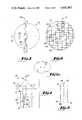
- FIG. 2is a block diagram of the particle position correlator of the present invention.
- FIG. 3is a top plan view of a wafer with particles being scanned by the detector in FIG. 1.
- FIG. 4is a graph of a Gaussian beam intensity distribution in conjunction with an enlarged plan view of the scanning of the wafer in FIG. 2.
- FIG. 5is a schematic illustration of the process of the present invention.
- FIG. 6is a plan view of a display of particles on the wafer in FIG. 3 in accord with the present invention.
- FIG. 6ais an enlarged pixel in FIG. 3 in accord with an alternate embodiment of the present invention.
- a low power laser 11may be seen directing a beam 13 toward mirror 15.
- Laser 11can be a helium-neon general purpose laser having an output power of a few milliwatts. A higher power laser may be preferable for greater detection capability. In some instances blue light, e.g. from a helium-cadmium laser is preferred for detection of smaller defects than with a helium-neon laser.
- Beam 13is directed to focussing lens 17 and then to a beam collimating and focussing lens 19.
- a spatial filter 18a short distance from lens 17 allows only the central portion of the beam to proceed.
- the focal length of lens 19is approximately 14 cm. From lens 19, the beam is directed toward fixed mirror 21 and then to galvanometer mirror 23.
- Galvonometer mirror 23directs light so that the focal point of the beam is at the surface of the surface 25.
- the focal length of focussing optics 19is long enough so that the beam stays in focus as it is swept across the surface 25, even though the beam makes a slightly arc-shaped trajectory. There is sufficient depth of field at this long focal length that a fine beam spot is maintained as the beam sweeps across the surface being scanned for defects. Because of this long focal length, the beam generally remains perpendicular to the surface 25 being scanned.
- the defectneed not be highly reflective. Reflectivity above 7 to 10% is sufficient to be detected with a low power, helium neon laser with a sensitive detector, such as a photomultiplier tube, and the light collector of the present invention.
- the light collector 27is a sector, preferably a quadrant, of a spherical shell.
- the shellhas a reflective coating, such as white paint, on the inside surface, facing surface 25, and an absorptive coating, such as black paint, on the outside surface.
- a reflective coatingsuch as white paint
- an absorptive coatingsuch as black paint
- FIG. 1For purposes of illustration, only one-half of the shell is shown in FIG. 1. That half is shown resting on mirror surface 31 which forms half of a V-shaped trough in which the shell 27 rests.
- Shell 27has a slit through which beam 13 enters. This slit is not visible in FIG. 1.
- the beampasses through an exit aperture 35, visible in Fig. 2, which is opposite the beam entrance aperture.
- the upper portion of the shellis termed a "crown".
- the inner crown surfacedirects light toward the mirrors, then back to the crown, and so on, until light enters the detector.
- the shellis positioned in proximity to the surface 25 with the crown distal to the test surface and the bottom of the V-shaped trough formed by the mirror side walls in close proximity to the test surface. This is done in order that a gap between the V-shaped walls, which forms the beam exit port, be very close to the test surface.
- close proximitywithin a few millimeters, allows most of the scattered light from the test surface to reenter the light collector. Specularly reflected light doubles back on the beam path toward the galvanometer mirror and is lost.
- light scattered at an angle to the incident beamis collected for measurement by the detector.
- the V-shaped mirror side wallshave two distinct functions. First, the walls serve to optically fold the sector, allowing for a compact collector. Second, the linear gap between the base of the side walls serves as a beam exit port for a scanning beam along a linear scanning path. Each of the side walls is inclined to the vertical by an angle of 45 degrees.
- the galvanometer mirror 23moves back and forth at a high rate, such as 400 sweeps per second, in directions indicated by the arrows A. This causes the beam to move back and forth across test surface 25 in the Y direction. Independently of this motion, surface 25 is advanced in the X direction by a transport 41 on which the test surface is carried. Sensors at each end of test surface detect the beginning and end of a scan line and reset a clock.
- the clocktypically operates at 16 MH and provides a Y-address for the scan beam within one clock cycle (62.5 nsec).
- particle data coming from a single scan lineare stored sequentially in an input buffer 43.
- buffer 43may have as many as 1024 storage locations.
- Particle data from previous scansare stored in a second buffer or memory 45 with an equal number of storage locations.
- Particle dataincludes a scattering amplitude value and a corresponding address made up of a scan line number and a Y-address.
- the peak amplitude of the scattered beamor alternatively the integrated amplitude, is digitized and sent to input buffer 43 as a scattering amplitude value, hereafter referred to as amplitude data.
- Both the input buffer 43 and memory 45are thus typically three bytes wide. One byte contains amplitude data while the other two bytes contain the address. Memory 45 is a combination of all the previous scan lines as will be explained below. Buffer 43 and memory 45 may be thought of as sequential files which represent particle detections and which are read in a top-down fashion.
- an address comparator 49receives a Y-address from both buffer 43 and memory 45. Comparator 49 compares a Y-address from buffer 43, representing the current scan line with a Y-address from memory 45, representing previous scan lines. Two Y-addresses are said "match", representing the same particle, when they are the same or different within a preset number of clock cycles from each other. Typically, the Y-addresses match when they are not more than one or two cycles apart.
- Y-addressesmatch, that is the current particle data has a corresponding previous particle datum
- the amplitude datais compared in a data comparator 51.
- Data comparator 51is corrected to receive the amplitude data from input buffer 43 and memory 45.
- the particle detection having a larger amplitude valueis stored with its address in memory 45, while the other amplitude data is discarded. If the amplitudes are equal, no exchange takes place. In this way, all detections of a particle are reduced or "fused" into one.
- a Y-address stored in a previous scan line file in memory 45lacks a matching Y-address in the current scan files in buffer 43, then a particle which previously had been detected is no longer seen by the beam.
- An amplitude comparisonis again made by data comparitor 51. Since there is no corresponding amplitude data in buffer 43, the comparison results in a transfer of the previous data to a FIFO stack 53. This entry is removed from memory 45.
- FIFO stackis connected to comparitors 49 and 51 and receives particle data only when all detections for a particle have been considered.
- An output buffer 55connects to FIFO stack 53 and sends data in FIFO 53 to computer storage via an external bus 57. The particle data in computer storage is ready for display, counting, or further processing by computer.
- a semiconductor wafer or other surface 61 to be scannedcontains particles 63 thereon. Particles 63 vary in size but are typically about one micrometer in diameter.
- a laser beamscans surface 61 in a back-and-forth series of sweeps 65. Each sweep takes about 2.5 milliseconds, there being about 400 sweep cycles per second.
- surface 61is transported in a direction orthogonal to the sweeps 65, as indicated by arrow 67. As a result, each sweep 65 is spatially separated on surface 61 from the preceding sweep thereby forming adjacent scan lines, such as lines 69 and 71. Each scan line is typically separated by about 25 micrometers.
- a scanning laser beam 72typically has a Gaussian intensity distribution
- I ois a peak intensity at the center of the beam 73 and W is the full width measured at 1/e 2 of the peak intensity.
- the scanning beamhas a full width, as represented in FIG. 4 by arrows A--A, of about 100 micrometers.
- the beam 72has a width substantially larger, usually four to six times larger, than the scan line separation.
- the thresholddepends on both the light gathering power of the surface scanning system and the sensitivity of the detector.
- the thresholdmay be adjusted by using a comparator that generates an amplitude value signal only when the received amplitude is above a preset value.
- the thresholdis typically adjusted to detect particles at lower scattering amplitudes and so that separate particles are not fused into one. In any case, the intensity of the beam striking a particle must be above a threshold value, indicated by dashed line 75 in FIG. 4, to detect the particle. A portion 77 of Gaussian beam 72 is below threshold.
- a particle 79is seen lying near a pixel boundary 81.
- Pixel boundaries 81 and 82are not physical features on the surface being scanned and are shown in FIG. 4 only for illustration.
- the current scan line 83is to the right of pixel boundary 81.
- Beam 72strikes particle 79 with an intensity above threshold 75, as seen by dashed line 85.
- particle 79is detected even though it does not lie in the pixel currently being scanned.
- Particle 79is also detected with a larger amplitude value by scanning a scan line 85.
- both pixels to the left and right of pixel boundary 81would be lit, indicating detection.
- the detection by scanning on scan line 83is discarded in favor of the larger amplitude value detected on scan line 85.
- the separate detectionsare fused by the position correlator described with reference to FIG. 2 into one detection yielding an accurate particle count.
- FIG. 5a schematic representation of detections on three scan lines 87, 89 and 91 illustrates the process of the present invention.
- Each Xrepresents a particle detection.
- Detections on the same horizontal rowrepresent detections in which Y-addresses match.
- scan line 89is scanned, particle detection data is received and stored in a buffer.
- Data from scan line 87 and prior scan linesare stored in a second buffer or memory.
- Detection 93represents a new particle since no corresponding detection in scan line 87 has a matching Y-address.
- Particle data relating to detection 93is stored in memory.
- Detection 95represents another detection of a previously detected particle.
- Detection 97 on scan line 89has a matching Y-address with detection 95.
- the amplitude data for detection 95 and the stored amplitude for scan line 87 or earlierare compared.
- Particle data for the detection data with the large amplitude datais stored in memory.
- Particle data for the other detectionis discarded.
- scan line 91no particle detection has a matching Y-address with detection 93.
- Data for detection 93is sent to a FIFO stack for delivery to computer storage.
- particle detection data in computer storageis displayed as pixels 103, 105, and 107 on a wafer 101.
- Each pixelhas a dimension substantially larger than the separation between scan lines, such as scan lines 96 and 71 in FIG. 3.
- scan lines 96 and 71 in FIG. 3.Typically, each pixel is a square 10 to 16 scan lines wide.
- a pixel 103for example, has 3 particles.
- a pixel 105is lit when at least one particle lies on the wafer in that pixel. Pixels, such as pixel 107, having no particle detections remain unlit.
- a pixel in FIG. 6is displayed in an enlarged format.
- Enlarged pixelshows each particle detected in a pixel.
- Each particle displayed in the enlarged pixelcorresponds to an address derived with the correlation process of the present invention. As a result, even particles spaced together closer than the beam width can be distinguished and displayed.
Landscapes
- Physics & Mathematics (AREA)
- Health & Medical Sciences (AREA)
- Life Sciences & Earth Sciences (AREA)
- Chemical & Material Sciences (AREA)
- Analytical Chemistry (AREA)
- Biochemistry (AREA)
- General Health & Medical Sciences (AREA)
- General Physics & Mathematics (AREA)
- Immunology (AREA)
- Pathology (AREA)
- Investigating Materials By The Use Of Optical Means Adapted For Particular Applications (AREA)
Abstract
Description
I(x)=I.sub.o exp{-(w/√2x).sup.2}Claims (14)
- .claims
- 1. A process of particle detection and position correlation comprising,(a) scanning a first scan line on a surface with a laser beam having a characteristic beam width, scattering of said laser beam from said surface being detected when a scattering amplitude is above a threshold value, a Y-address of said scanning beam being generated during said scanning,(b) storing data from said scanning of said first line, as previous data, said data identifying an address having a scan line number and a Y-address, said data also including scattering amplitude data at each said address,(c) scanning a second line with said laser beam, said second scan line being spaced a distance less than the beam width from said first scan line, scattering of said beam again being detected, data from said scanning of said second line being stored as current data,(d) comparing said current data with said previous data, current data that lack a corresponding previous datum with a matching Y-address being stored as previous data, said current data having a corresponding previous datum with a matching Y-address replacing said previous datum when said amplitude data of said current data has a value larger than that of said previous datum,(e) sending previous data that lack a corresponding current datum with a matching Y-address to a computer storage, and(f) repeating steps (c)-(e) for third, fourth and succeeding scan lines until the entire surface is scanned.
- 2. The process of claim 1 further comprising counting between step (d) and step (e) the number of scan lines with a particular Y-address corresponding to a particular particle detection, said previous data being sent in step (f) only when said number of scan lines counted is in a preset range, said previous data lacking a corresponding current datum with a matching Y-address being discarded when said number of scan lines counted is outside said preset range.
- 3. The process of claim 2 wherein said preset range has a lower limit of two corresponding to noise and an upper limit of twelve corresponding to a surface line.
- 4. The process of claim 1 further comprising displaying said data in computer storage or a grid of pixels, said pixels having a characteristic dimension substantially larger than said separation between succeeding scan lines, a pixel being lit when at least one address corresponding to a pixel is in computer storage.
- 5. The process of claim 4 further comprising enlarging at least one of said lit pixels, said pixel having a plurality of subelements, each subelement corresponding to an address, a subelement being lit when said corresponding address is in computer storage.
- 6. A particle position correlator for use in a surface scanner comprising,means for receiving addresses and corresponding scattering amplitude data relating to particle detection on a current scan line,means for storing said addresses and data, some of said addresses matching addresses stored from previous scan lines, the rest of such addresses corresponding to new particle detections,means for comparing said addresses and said amplitude data relating to said current scan line with said addresses and corresponding amplitude data stored from said previous scan lines, said amplitude data being compared when said compared addresses match, one of said compared amplitude data having a larger amplitude value being stored in said storing means with the address to which said one corresponds, the other of said compared amplitude data and the address to which the other corresponds being discarded, andmeans for sending said addresses and data stored from previous scan lines that lack a matching address relating to said current scan line to an output for computer storage, said sent addresses and data corresponding to finished particle detections.
- 7. The particle position correlator of claim 6 wherein said receiving means comprises an input buffer receiving amplitude data relating to a current scan line from a light detector in a surface scanner, said input buffer connected to said storing means storing said addresses and data and to said comparing means.
- 8. The particle position correlator of claim 6 wherein said sending means comprises a FIFO stack connected on an input end to said comparing means, and an output buffer connected to an output end of said FIFO stack to receive addresses and data to be sent and connected via an external bus to a computer storage.
- 9. The particle position correlator of claim 6 further comprising a means for counting the number of scan lines with a particular address corresponding to a particle detection, said addresses and data stored from previous scan lines that lack a matching address relating to a current scan line being discarded when the number of scan lines counted for said addresses is outside a preset range.
- 10. The particle position correlator of claim 9 wherein said preset range has a lower limit of two corresponding to noise and an upper limit of twelve corresponding to a detected surface line.
- 11. The particle position correlator of claim 6 wherein said addresses comprise a scan line number and a sweep clock count.
- 12. A particle position correlator for use in a surface scanner comprising,an input buffer receiving scattering amplitude data relating to particle detection on a current scan line from a light detector in a surface scanner and receiving addresses corresponding to said data, each of said addresses including at least a scan line number and a Y-address,means connected to said input buffer for storing said addresses and data, some of said addresses matching addresses stored in said storing means from previous scan lines, the rest of said addresses corresponding to new particle detections,means connected to said input buffer and to said storing means for comparing said addresses and said corresponding amplitude data relating to said current scan line with said addresses and corresponding amplitude data stored in said storing means from said previous scan lines, said corresponding amplitude data being compared when said compared addresses have matching Y-addresses, one of said compared amplitude data having a larger amplitude value being stored in said storing means with the address to which said one corresponds, the other of said compared amplitude data and the address to which said other corresponds being discarded,means for counting the number of scan lines with a particular Y-address corresponding to each particle detection,a FIFO stack connected at an input end to said comparing means, and an output buffer connected to an output end of said FIFO stack and connected via an external bus to a computer storage, said addresses and data stored from previous scan lines that lack a matching Y address relating to a current scan line being sent to said computer storage via said FIFO stack and said output buffer when the number of scan lines counted for said particular Y-address is in a preset range, and being discarded when the number of scan lines counted for said particular Y-address is outset said preset range.
- 13. The particle position correlator of claim 12 wherein said preset range has a lower limit of two corresponding to noise and an upper limit of twelve corresponding to a detected surface line.
Priority Applications (1)
| Application Number | Priority Date | Filing Date | Title |
|---|---|---|---|
| US06/786,620US4641967A (en) | 1985-10-11 | 1985-10-11 | Particle position correlator and correlation method for a surface scanner |
Applications Claiming Priority (1)
| Application Number | Priority Date | Filing Date | Title |
|---|---|---|---|
| US06/786,620US4641967A (en) | 1985-10-11 | 1985-10-11 | Particle position correlator and correlation method for a surface scanner |
Publications (1)
| Publication Number | Publication Date |
|---|---|
| US4641967Atrue US4641967A (en) | 1987-02-10 |
Family
ID=25139122
Family Applications (1)
| Application Number | Title | Priority Date | Filing Date |
|---|---|---|---|
| US06/786,620Expired - LifetimeUS4641967A (en) | 1985-10-11 | 1985-10-11 | Particle position correlator and correlation method for a surface scanner |
Country Status (1)
| Country | Link |
|---|---|
| US (1) | US4641967A (en) |
Cited By (63)
| Publication number | Priority date | Publication date | Assignee | Title |
|---|---|---|---|---|
| US5003495A (en)* | 1987-07-27 | 1991-03-26 | Visual Understanding Systems, Inc. | Method and apparatus for scanning, storing and reproducing artwork |
| US5355212A (en)* | 1993-07-19 | 1994-10-11 | Tencor Instruments | Process for inspecting patterned wafers |
| US5631733A (en)* | 1995-01-20 | 1997-05-20 | Photon Dynamics, Inc. | Large area defect monitor tool for manufacture of clean surfaces |
| US5801824A (en)* | 1996-11-25 | 1998-09-01 | Photon Dynamics, Inc. | Large area defect monitor tool for manufacture of clean surfaces |
| US6198982B1 (en)* | 1997-06-05 | 2001-03-06 | Samsung Electronics Co., Ltd. | Method and apparatus for detecting the presence of particles on a wafer holder of semiconductor exposure equipment |
| US6204918B1 (en)* | 1998-04-13 | 2001-03-20 | Kabushiki Kaisha Topcon | Apparatus for surface inspection |
| US6356653B2 (en)* | 1998-07-16 | 2002-03-12 | International Business Machines Corporation | Method and apparatus for combined particle location and removal |
| EP1113262A3 (en)* | 1999-12-03 | 2002-04-10 | Sony Corporation | Inspection apparatus and method |
| US20020103564A1 (en)* | 2000-09-20 | 2002-08-01 | John Fielden | Methods and systems for determining a composition and a thickness of a specimen |
| US20020106848A1 (en)* | 2000-09-20 | 2002-08-08 | Dan Wack | Methods and systems for determining a property of a specimen prior to, during, or subsequent to lithography |
| US20020107650A1 (en)* | 2000-09-20 | 2002-08-08 | Dan Wack | Methods and systems for determining a critical dimension and a presence of defects on a specimen |
| US20020186368A1 (en)* | 2001-06-08 | 2002-12-12 | Eliezer Rosengaus | Systems and methods for inspection of specimen surfaces |
| US20030139838A1 (en)* | 2002-01-16 | 2003-07-24 | Marella Paul Frank | Systems and methods for closed loop defect reduction |
| US6673637B2 (en) | 2000-09-20 | 2004-01-06 | Kla-Tencor Technologies | Methods and systems for determining a presence of macro defects and overlay of a specimen |
| US6694284B1 (en) | 2000-09-20 | 2004-02-17 | Kla-Tencor Technologies Corp. | Methods and systems for determining at least four properties of a specimen |
| US20040032581A1 (en)* | 2002-01-15 | 2004-02-19 | Mehrdad Nikoonahad | Systems and methods for inspection of specimen surfaces |
| US20040117055A1 (en)* | 2001-05-17 | 2004-06-17 | Torsten Seidel | Configuration and method for detecting defects on a substrate in a processing tool |
| US6812045B1 (en) | 2000-09-20 | 2004-11-02 | Kla-Tencor, Inc. | Methods and systems for determining a characteristic of a specimen prior to, during, or subsequent to ion implantation |
| US20040235205A1 (en)* | 2000-09-20 | 2004-11-25 | Kla-Tencor, Inc. | Methods and systems for determining a critical dimension and overlay of a specimen |
| US6919957B2 (en) | 2000-09-20 | 2005-07-19 | Kla-Tencor Technologies Corp. | Methods and systems for determining a critical dimension, a presence of defects, and a thin film characteristic of a specimen |
| US20050205807A1 (en)* | 2004-03-18 | 2005-09-22 | Perel Alexander S | In-situ monitoring on an ion implanter |
| US20050259805A1 (en)* | 2000-10-30 | 2005-11-24 | Yoichi Okudera | Telephone directory assistane method and telephone directory assistance system |
| US20060062445A1 (en)* | 2004-09-14 | 2006-03-23 | Gaurav Verma | Methods, systems, and carrier media for evaluating reticle layout data |
| US7027143B1 (en) | 2002-10-15 | 2006-04-11 | Kla-Tencor Technologies Corp. | Methods and systems for inspecting reticles using aerial imaging at off-stepper wavelengths |
| US20060150841A1 (en)* | 2005-01-07 | 2006-07-13 | Heidelberger Druckmaschinen Ag | Printing press |
| US20060161452A1 (en)* | 2004-01-29 | 2006-07-20 | Kla-Tencor Technologies Corp. | Computer-implemented methods, processors, and systems for creating a wafer fabrication process |
| US7106425B1 (en) | 2000-09-20 | 2006-09-12 | Kla-Tencor Technologies Corp. | Methods and systems for determining a presence of defects and a thin film characteristic of a specimen |
| US7123356B1 (en) | 2002-10-15 | 2006-10-17 | Kla-Tencor Technologies Corp. | Methods and systems for inspecting reticles using aerial imaging and die-to-database detection |
| US7130029B2 (en) | 2000-09-20 | 2006-10-31 | Kla-Tencor Technologies Corp. | Methods and systems for determining an adhesion characteristic and a thickness of a specimen |
| US7133119B1 (en) | 2002-12-17 | 2006-11-07 | Kla-Tencor Technologies Corp. | Systems for simulating high NA and polarization effects in aerial images |
| US20070156379A1 (en)* | 2005-11-18 | 2007-07-05 | Ashok Kulkarni | Methods and systems for utilizing design data in combination with inspection data |
| US20070230770A1 (en)* | 2005-11-18 | 2007-10-04 | Ashok Kulkarni | Methods and systems for determining a position of inspection data in design data space |
| EP1777511A3 (en)* | 1994-12-08 | 2007-12-12 | KLA-Tencor Corporation | Scanning system for inspecting anomalies on surfaces |
| US20070288219A1 (en)* | 2005-11-18 | 2007-12-13 | Khurram Zafar | Methods and systems for utilizing design data in combination with inspection data |
| US7379175B1 (en) | 2002-10-15 | 2008-05-27 | Kla-Tencor Technologies Corp. | Methods and systems for reticle inspection and defect review using aerial imaging |
| US20080167829A1 (en)* | 2007-01-05 | 2008-07-10 | Allen Park | Methods and systems for using electrical information for a device being fabricated on a wafer to perform one or more defect-related functions |
| US20080304056A1 (en)* | 2007-05-07 | 2008-12-11 | David Alles | Methods for detecting and classifying defects on a reticle |
| US20090016595A1 (en)* | 2007-05-09 | 2009-01-15 | Peterson Ingrid B | Methods and systems for detecting defects in a reticle design pattern |
| US20090024967A1 (en)* | 2007-05-07 | 2009-01-22 | Bo Su | Computer-implemented methods, systems, and computer-readable media for determining a model for predicting printability of reticle features on a wafer |
| US20090041332A1 (en)* | 2007-07-20 | 2009-02-12 | Kla-Tencor Corporation | Methods for generating a standard reference die for use in a die to standard reference die inspection and methods for inspecting a wafer |
| US20090043527A1 (en)* | 2007-08-10 | 2009-02-12 | Allen Park | Computer-implemented methods, carrier media, and systems for generating a metrology sampling plan |
| US20090055783A1 (en)* | 2007-08-20 | 2009-02-26 | Kla-Tencor Corporation | Computer-implemented methods for determining if actual defects are potentially systematic defects or potentially random defects |
| US20090257645A1 (en)* | 2008-04-14 | 2009-10-15 | Chen Chien-Huei Adam | Methods and systems for determining a defect criticality index for defects on wafers |
| US7769225B2 (en) | 2005-08-02 | 2010-08-03 | Kla-Tencor Technologies Corp. | Methods and systems for detecting defects in a reticle design pattern |
| US20100235134A1 (en)* | 2009-03-13 | 2010-09-16 | Kla-Tencor Corporation | Methods and systems for generating an inspection process for a wafer |
| US7877722B2 (en) | 2006-12-19 | 2011-01-25 | Kla-Tencor Corp. | Systems and methods for creating inspection recipes |
| US20110187848A1 (en)* | 2008-07-28 | 2011-08-04 | Kla-Tencor Corporation | Computer-implemented methods, computer-readable media, and systems for classifying defects detected in a memory device area on a wafer |
| US8204297B1 (en) | 2009-02-27 | 2012-06-19 | Kla-Tencor Corp. | Methods and systems for classifying defects detected on a reticle |
| US8775101B2 (en) | 2009-02-13 | 2014-07-08 | Kla-Tencor Corp. | Detecting defects on a wafer |
| US8781781B2 (en) | 2010-07-30 | 2014-07-15 | Kla-Tencor Corp. | Dynamic care areas |
| US8826200B2 (en) | 2012-05-25 | 2014-09-02 | Kla-Tencor Corp. | Alteration for wafer inspection |
| US8831334B2 (en) | 2012-01-20 | 2014-09-09 | Kla-Tencor Corp. | Segmentation for wafer inspection |
| US8995066B2 (en) | 2011-09-06 | 2015-03-31 | Kla-Tencor Corporation | Passive position compensation of a spindle, stage, or component exposed to a heat load |
| US9053527B2 (en) | 2013-01-02 | 2015-06-09 | Kla-Tencor Corp. | Detecting defects on a wafer |
| US9087367B2 (en) | 2011-09-13 | 2015-07-21 | Kla-Tencor Corp. | Determining design coordinates for wafer defects |
| US9092846B2 (en) | 2013-02-01 | 2015-07-28 | Kla-Tencor Corp. | Detecting defects on a wafer using defect-specific and multi-channel information |
| US9134254B2 (en) | 2013-01-07 | 2015-09-15 | Kla-Tencor Corp. | Determining a position of inspection system output in design data space |
| US9170211B2 (en) | 2011-03-25 | 2015-10-27 | Kla-Tencor Corp. | Design-based inspection using repeating structures |
| US9189844B2 (en) | 2012-10-15 | 2015-11-17 | Kla-Tencor Corp. | Detecting defects on a wafer using defect-specific information |
| CN105445283A (en)* | 2016-02-01 | 2016-03-30 | 成都通甲优博科技有限责任公司 | Detection method for filthy conditions of insulator images |
| US9311698B2 (en) | 2013-01-09 | 2016-04-12 | Kla-Tencor Corp. | Detecting defects on a wafer using template image matching |
| US9310320B2 (en) | 2013-04-15 | 2016-04-12 | Kla-Tencor Corp. | Based sampling and binning for yield critical defects |
| US9865512B2 (en) | 2013-04-08 | 2018-01-09 | Kla-Tencor Corp. | Dynamic design attributes for wafer inspection |
Citations (1)
| Publication number | Priority date | Publication date | Assignee | Title |
|---|---|---|---|---|
| US4559603A (en)* | 1982-10-05 | 1985-12-17 | Tokyo Shibaura Denki Kabushiki Kaisha | Apparatus for inspecting a circuit pattern drawn on a photomask used in manufacturing large scale integrated circuits |
- 1985
- 1985-10-11USUS06/786,620patent/US4641967A/ennot_activeExpired - Lifetime
Patent Citations (1)
| Publication number | Priority date | Publication date | Assignee | Title |
|---|---|---|---|---|
| US4559603A (en)* | 1982-10-05 | 1985-12-17 | Tokyo Shibaura Denki Kabushiki Kaisha | Apparatus for inspecting a circuit pattern drawn on a photomask used in manufacturing large scale integrated circuits |
Non-Patent Citations (1)
| Title |
|---|
| Untitled article by A. Neukermans, dated Jan. 13, 1986.* |
Cited By (115)
| Publication number | Priority date | Publication date | Assignee | Title |
|---|---|---|---|---|
| US5003495A (en)* | 1987-07-27 | 1991-03-26 | Visual Understanding Systems, Inc. | Method and apparatus for scanning, storing and reproducing artwork |
| US5355212A (en)* | 1993-07-19 | 1994-10-11 | Tencor Instruments | Process for inspecting patterned wafers |
| EP1777511A3 (en)* | 1994-12-08 | 2007-12-12 | KLA-Tencor Corporation | Scanning system for inspecting anomalies on surfaces |
| US5631733A (en)* | 1995-01-20 | 1997-05-20 | Photon Dynamics, Inc. | Large area defect monitor tool for manufacture of clean surfaces |
| US5801824A (en)* | 1996-11-25 | 1998-09-01 | Photon Dynamics, Inc. | Large area defect monitor tool for manufacture of clean surfaces |
| US6198982B1 (en)* | 1997-06-05 | 2001-03-06 | Samsung Electronics Co., Ltd. | Method and apparatus for detecting the presence of particles on a wafer holder of semiconductor exposure equipment |
| US6204918B1 (en)* | 1998-04-13 | 2001-03-20 | Kabushiki Kaisha Topcon | Apparatus for surface inspection |
| US6356653B2 (en)* | 1998-07-16 | 2002-03-12 | International Business Machines Corporation | Method and apparatus for combined particle location and removal |
| US6559937B2 (en) | 1999-12-03 | 2003-05-06 | Sony Corporation | Inspection apparatus and method |
| EP1113262A3 (en)* | 1999-12-03 | 2002-04-10 | Sony Corporation | Inspection apparatus and method |
| US6891627B1 (en) | 2000-09-20 | 2005-05-10 | Kla-Tencor Technologies Corp. | Methods and systems for determining a critical dimension and overlay of a specimen |
| US6950196B2 (en) | 2000-09-20 | 2005-09-27 | Kla-Tencor Technologies Corp. | Methods and systems for determining a thickness of a structure on a specimen and at least one additional property of the specimen |
| US7751046B2 (en) | 2000-09-20 | 2010-07-06 | Kla-Tencor Technologies Corp. | Methods and systems for determining a critical dimension and overlay of a specimen |
| US20020190207A1 (en)* | 2000-09-20 | 2002-12-19 | Ady Levy | Methods and systems for determining a characteristic of micro defects on a specimen |
| US20030011786A1 (en)* | 2000-09-20 | 2003-01-16 | Ady Levy | Methods and systems for determining overlay and flatness of a specimen |
| US20020107650A1 (en)* | 2000-09-20 | 2002-08-08 | Dan Wack | Methods and systems for determining a critical dimension and a presence of defects on a specimen |
| US7460981B2 (en) | 2000-09-20 | 2008-12-02 | Kla-Tencor Technologies Corp. | Methods and systems for determining a presence of macro and micro defects on a specimen |
| US6633831B2 (en) | 2000-09-20 | 2003-10-14 | Kla Tencor Technologies | Methods and systems for determining a critical dimension and a thin film characteristic of a specimen |
| US6673637B2 (en) | 2000-09-20 | 2004-01-06 | Kla-Tencor Technologies | Methods and systems for determining a presence of macro defects and overlay of a specimen |
| US6694284B1 (en) | 2000-09-20 | 2004-02-17 | Kla-Tencor Technologies Corp. | Methods and systems for determining at least four properties of a specimen |
| US7349090B2 (en) | 2000-09-20 | 2008-03-25 | Kla-Tencor Technologies Corp. | Methods and systems for determining a property of a specimen prior to, during, or subsequent to lithography |
| US20040073398A1 (en)* | 2000-09-20 | 2004-04-15 | Kla-Tencor, Inc. | Methods and systems for determining a critical dimension and a thin film characteristic of a specimen |
| US20040092045A1 (en)* | 2000-09-20 | 2004-05-13 | Gary Bultman | Methods and systems for determining a presence of macro and micro defects on a specimen |
| US8179530B2 (en) | 2000-09-20 | 2012-05-15 | Kla-Tencor Technologies Corp. | Methods and systems for determining a critical dimension and overlay of a specimen |
| US20040115843A1 (en)* | 2000-09-20 | 2004-06-17 | Kla-Tencor, Inc. | Methods and systems for determining a presence of macro defects and overlay of a specimen |
| US6782337B2 (en) | 2000-09-20 | 2004-08-24 | Kla-Tencor Technologies Corp. | Methods and systems for determining a critical dimension an a presence of defects on a specimen |
| US6806951B2 (en) | 2000-09-20 | 2004-10-19 | Kla-Tencor Technologies Corp. | Methods and systems for determining at least one characteristic of defects on at least two sides of a specimen |
| US6812045B1 (en) | 2000-09-20 | 2004-11-02 | Kla-Tencor, Inc. | Methods and systems for determining a characteristic of a specimen prior to, during, or subsequent to ion implantation |
| US6818459B2 (en) | 2000-09-20 | 2004-11-16 | Kla-Tencor Technologies Corp. | Methods and systems for determining a presence of macro defects and overlay of a specimen |
| US20040235205A1 (en)* | 2000-09-20 | 2004-11-25 | Kla-Tencor, Inc. | Methods and systems for determining a critical dimension and overlay of a specimen |
| US6829559B2 (en) | 2000-09-20 | 2004-12-07 | K.L.A.-Tencor Technologies | Methods and systems for determining a presence of macro and micro defects on a specimen |
| US6891610B2 (en) | 2000-09-20 | 2005-05-10 | Kla-Tencor Technologies Corp. | Methods and systems for determining an implant characteristic and a presence of defects on a specimen |
| US20020103564A1 (en)* | 2000-09-20 | 2002-08-01 | John Fielden | Methods and systems for determining a composition and a thickness of a specimen |
| US6917433B2 (en) | 2000-09-20 | 2005-07-12 | Kla-Tencor Technologies Corp. | Methods and systems for determining a property of a specimen prior to, during, or subsequent to an etch process |
| US6917419B2 (en) | 2000-09-20 | 2005-07-12 | Kla-Tencor Technologies Corp. | Methods and systems for determining flatness, a presence of defects, and a thin film characteristic of a specimen |
| US6919957B2 (en) | 2000-09-20 | 2005-07-19 | Kla-Tencor Technologies Corp. | Methods and systems for determining a critical dimension, a presence of defects, and a thin film characteristic of a specimen |
| US6946394B2 (en) | 2000-09-20 | 2005-09-20 | Kla-Tencor Technologies | Methods and systems for determining a characteristic of a layer formed on a specimen by a deposition process |
| US8502979B2 (en) | 2000-09-20 | 2013-08-06 | Kla-Tencor Technologies Corp. | Methods and systems for determining a critical dimension and overlay of a specimen |
| US20020179867A1 (en)* | 2000-09-20 | 2002-12-05 | John Fielden | Methods and systems for determining flatness, a presence of defects, and a thin film characteristic of a specimen |
| US20020106848A1 (en)* | 2000-09-20 | 2002-08-08 | Dan Wack | Methods and systems for determining a property of a specimen prior to, during, or subsequent to lithography |
| US7006235B2 (en) | 2000-09-20 | 2006-02-28 | Kla-Tencor Technologies Corp. | Methods and systems for determining overlay and flatness of a specimen |
| US7196782B2 (en) | 2000-09-20 | 2007-03-27 | Kla-Tencor Technologies Corp. | Methods and systems for determining a thin film characteristic and an electrical property of a specimen |
| US20060072807A1 (en)* | 2000-09-20 | 2006-04-06 | Kla-Tencor Technologies. | Methods and systems for determining a presence of macro and micro defects on a specimen |
| US7139083B2 (en) | 2000-09-20 | 2006-11-21 | Kla-Tencor Technologies Corp. | Methods and systems for determining a composition and a thickness of a specimen |
| US7130029B2 (en) | 2000-09-20 | 2006-10-31 | Kla-Tencor Technologies Corp. | Methods and systems for determining an adhesion characteristic and a thickness of a specimen |
| US7106425B1 (en) | 2000-09-20 | 2006-09-12 | Kla-Tencor Technologies Corp. | Methods and systems for determining a presence of defects and a thin film characteristic of a specimen |
| US20050259805A1 (en)* | 2000-10-30 | 2005-11-24 | Yoichi Okudera | Telephone directory assistane method and telephone directory assistance system |
| US20040117055A1 (en)* | 2001-05-17 | 2004-06-17 | Torsten Seidel | Configuration and method for detecting defects on a substrate in a processing tool |
| US7072034B2 (en) | 2001-06-08 | 2006-07-04 | Kla-Tencor Corporation | Systems and methods for inspection of specimen surfaces |
| US20020186368A1 (en)* | 2001-06-08 | 2002-12-12 | Eliezer Rosengaus | Systems and methods for inspection of specimen surfaces |
| US20040032581A1 (en)* | 2002-01-15 | 2004-02-19 | Mehrdad Nikoonahad | Systems and methods for inspection of specimen surfaces |
| US7236847B2 (en) | 2002-01-16 | 2007-06-26 | Kla-Tencor Technologies Corp. | Systems and methods for closed loop defect reduction |
| US20030139838A1 (en)* | 2002-01-16 | 2003-07-24 | Marella Paul Frank | Systems and methods for closed loop defect reduction |
| US7379175B1 (en) | 2002-10-15 | 2008-05-27 | Kla-Tencor Technologies Corp. | Methods and systems for reticle inspection and defect review using aerial imaging |
| US7027143B1 (en) | 2002-10-15 | 2006-04-11 | Kla-Tencor Technologies Corp. | Methods and systems for inspecting reticles using aerial imaging at off-stepper wavelengths |
| US7123356B1 (en) | 2002-10-15 | 2006-10-17 | Kla-Tencor Technologies Corp. | Methods and systems for inspecting reticles using aerial imaging and die-to-database detection |
| US7133119B1 (en) | 2002-12-17 | 2006-11-07 | Kla-Tencor Technologies Corp. | Systems for simulating high NA and polarization effects in aerial images |
| US7646906B2 (en) | 2004-01-29 | 2010-01-12 | Kla-Tencor Technologies Corp. | Computer-implemented methods for detecting defects in reticle design data |
| US20060161452A1 (en)* | 2004-01-29 | 2006-07-20 | Kla-Tencor Technologies Corp. | Computer-implemented methods, processors, and systems for creating a wafer fabrication process |
| US20060236294A1 (en)* | 2004-01-29 | 2006-10-19 | Saidin Zain K | Computer-implemented methods for detecting defects in reticle design data |
| US20050205807A1 (en)* | 2004-03-18 | 2005-09-22 | Perel Alexander S | In-situ monitoring on an ion implanter |
| US7078712B2 (en) | 2004-03-18 | 2006-07-18 | Axcelis Technologies, Inc. | In-situ monitoring on an ion implanter |
| US20060062445A1 (en)* | 2004-09-14 | 2006-03-23 | Gaurav Verma | Methods, systems, and carrier media for evaluating reticle layout data |
| US7689966B2 (en) | 2004-09-14 | 2010-03-30 | Kla-Tencor Technologies Corp. | Methods, systems, and carrier media for evaluating reticle layout data |
| US20060150841A1 (en)* | 2005-01-07 | 2006-07-13 | Heidelberger Druckmaschinen Ag | Printing press |
| US7769225B2 (en) | 2005-08-02 | 2010-08-03 | Kla-Tencor Technologies Corp. | Methods and systems for detecting defects in a reticle design pattern |
| US20070156379A1 (en)* | 2005-11-18 | 2007-07-05 | Ashok Kulkarni | Methods and systems for utilizing design data in combination with inspection data |
| US20070288219A1 (en)* | 2005-11-18 | 2007-12-13 | Khurram Zafar | Methods and systems for utilizing design data in combination with inspection data |
| US8139843B2 (en) | 2005-11-18 | 2012-03-20 | Kla-Tencor Technologies Corp. | Methods and systems for utilizing design data in combination with inspection data |
| US7570796B2 (en) | 2005-11-18 | 2009-08-04 | Kla-Tencor Technologies Corp. | Methods and systems for utilizing design data in combination with inspection data |
| US8923600B2 (en) | 2005-11-18 | 2014-12-30 | Kla-Tencor Technologies Corp. | Methods and systems for utilizing design data in combination with inspection data |
| US20090297019A1 (en)* | 2005-11-18 | 2009-12-03 | Kla-Tencor Technologies Corporation | Methods and systems for utilizing design data in combination with inspection data |
| US8041103B2 (en) | 2005-11-18 | 2011-10-18 | Kla-Tencor Technologies Corp. | Methods and systems for determining a position of inspection data in design data space |
| US7676077B2 (en) | 2005-11-18 | 2010-03-09 | Kla-Tencor Technologies Corp. | Methods and systems for utilizing design data in combination with inspection data |
| US20070230770A1 (en)* | 2005-11-18 | 2007-10-04 | Ashok Kulkarni | Methods and systems for determining a position of inspection data in design data space |
| US20100119144A1 (en)* | 2005-11-18 | 2010-05-13 | Kla-Tencor Technologies Corporation | Methods and systems for utilizing design data in combination with inspection data |
| US7877722B2 (en) | 2006-12-19 | 2011-01-25 | Kla-Tencor Corp. | Systems and methods for creating inspection recipes |
| US8194968B2 (en) | 2007-01-05 | 2012-06-05 | Kla-Tencor Corp. | Methods and systems for using electrical information for a device being fabricated on a wafer to perform one or more defect-related functions |
| US20080167829A1 (en)* | 2007-01-05 | 2008-07-10 | Allen Park | Methods and systems for using electrical information for a device being fabricated on a wafer to perform one or more defect-related functions |
| US20080304056A1 (en)* | 2007-05-07 | 2008-12-11 | David Alles | Methods for detecting and classifying defects on a reticle |
| US7962863B2 (en) | 2007-05-07 | 2011-06-14 | Kla-Tencor Corp. | Computer-implemented methods, systems, and computer-readable media for determining a model for predicting printability of reticle features on a wafer |
| US7738093B2 (en) | 2007-05-07 | 2010-06-15 | Kla-Tencor Corp. | Methods for detecting and classifying defects on a reticle |
| US20090024967A1 (en)* | 2007-05-07 | 2009-01-22 | Bo Su | Computer-implemented methods, systems, and computer-readable media for determining a model for predicting printability of reticle features on a wafer |
| US8213704B2 (en) | 2007-05-09 | 2012-07-03 | Kla-Tencor Corp. | Methods and systems for detecting defects in a reticle design pattern |
| US20090016595A1 (en)* | 2007-05-09 | 2009-01-15 | Peterson Ingrid B | Methods and systems for detecting defects in a reticle design pattern |
| US8204296B2 (en) | 2007-07-20 | 2012-06-19 | Kla-Tencor Corp. | Methods for generating a standard reference die for use in a die to standard reference die inspection and methods for inspecting a wafer |
| US20100329540A1 (en)* | 2007-07-20 | 2010-12-30 | Kla-Tencor Corporation | Methods for generating a standard reference die for use in a die to standard reference die inspection and methods for inspecting a wafer |
| US7796804B2 (en) | 2007-07-20 | 2010-09-14 | Kla-Tencor Corp. | Methods for generating a standard reference die for use in a die to standard reference die inspection and methods for inspecting a wafer |
| US20090041332A1 (en)* | 2007-07-20 | 2009-02-12 | Kla-Tencor Corporation | Methods for generating a standard reference die for use in a die to standard reference die inspection and methods for inspecting a wafer |
| US7711514B2 (en) | 2007-08-10 | 2010-05-04 | Kla-Tencor Technologies Corp. | Computer-implemented methods, carrier media, and systems for generating a metrology sampling plan |
| US20090043527A1 (en)* | 2007-08-10 | 2009-02-12 | Allen Park | Computer-implemented methods, carrier media, and systems for generating a metrology sampling plan |
| US7975245B2 (en) | 2007-08-20 | 2011-07-05 | Kla-Tencor Corp. | Computer-implemented methods for determining if actual defects are potentially systematic defects or potentially random defects |
| US20090055783A1 (en)* | 2007-08-20 | 2009-02-26 | Kla-Tencor Corporation | Computer-implemented methods for determining if actual defects are potentially systematic defects or potentially random defects |
| US8139844B2 (en) | 2008-04-14 | 2012-03-20 | Kla-Tencor Corp. | Methods and systems for determining a defect criticality index for defects on wafers |
| US20090257645A1 (en)* | 2008-04-14 | 2009-10-15 | Chen Chien-Huei Adam | Methods and systems for determining a defect criticality index for defects on wafers |
| US20110187848A1 (en)* | 2008-07-28 | 2011-08-04 | Kla-Tencor Corporation | Computer-implemented methods, computer-readable media, and systems for classifying defects detected in a memory device area on a wafer |
| US9659670B2 (en) | 2008-07-28 | 2017-05-23 | Kla-Tencor Corp. | Computer-implemented methods, computer-readable media, and systems for classifying defects detected in a memory device area on a wafer |
| US8775101B2 (en) | 2009-02-13 | 2014-07-08 | Kla-Tencor Corp. | Detecting defects on a wafer |
| US8204297B1 (en) | 2009-02-27 | 2012-06-19 | Kla-Tencor Corp. | Methods and systems for classifying defects detected on a reticle |
| US8112241B2 (en) | 2009-03-13 | 2012-02-07 | Kla-Tencor Corp. | Methods and systems for generating an inspection process for a wafer |
| US20100235134A1 (en)* | 2009-03-13 | 2010-09-16 | Kla-Tencor Corporation | Methods and systems for generating an inspection process for a wafer |
| US8781781B2 (en) | 2010-07-30 | 2014-07-15 | Kla-Tencor Corp. | Dynamic care areas |
| US9170211B2 (en) | 2011-03-25 | 2015-10-27 | Kla-Tencor Corp. | Design-based inspection using repeating structures |
| US8995066B2 (en) | 2011-09-06 | 2015-03-31 | Kla-Tencor Corporation | Passive position compensation of a spindle, stage, or component exposed to a heat load |
| US9087367B2 (en) | 2011-09-13 | 2015-07-21 | Kla-Tencor Corp. | Determining design coordinates for wafer defects |
| US8831334B2 (en) | 2012-01-20 | 2014-09-09 | Kla-Tencor Corp. | Segmentation for wafer inspection |
| US8826200B2 (en) | 2012-05-25 | 2014-09-02 | Kla-Tencor Corp. | Alteration for wafer inspection |
| US9189844B2 (en) | 2012-10-15 | 2015-11-17 | Kla-Tencor Corp. | Detecting defects on a wafer using defect-specific information |
| US9053527B2 (en) | 2013-01-02 | 2015-06-09 | Kla-Tencor Corp. | Detecting defects on a wafer |
| US9134254B2 (en) | 2013-01-07 | 2015-09-15 | Kla-Tencor Corp. | Determining a position of inspection system output in design data space |
| US9311698B2 (en) | 2013-01-09 | 2016-04-12 | Kla-Tencor Corp. | Detecting defects on a wafer using template image matching |
| US9092846B2 (en) | 2013-02-01 | 2015-07-28 | Kla-Tencor Corp. | Detecting defects on a wafer using defect-specific and multi-channel information |
| US9865512B2 (en) | 2013-04-08 | 2018-01-09 | Kla-Tencor Corp. | Dynamic design attributes for wafer inspection |
| US9310320B2 (en) | 2013-04-15 | 2016-04-12 | Kla-Tencor Corp. | Based sampling and binning for yield critical defects |
| CN105445283A (en)* | 2016-02-01 | 2016-03-30 | 成都通甲优博科技有限责任公司 | Detection method for filthy conditions of insulator images |
Similar Documents
| Publication | Publication Date | Title |
|---|---|---|
| US4641967A (en) | Particle position correlator and correlation method for a surface scanner | |
| US4766324A (en) | Particle detection method including comparison between sequential scans | |
| US4378159A (en) | Scanning contaminant and defect detector | |
| US4895446A (en) | Particle detection method and apparatus | |
| US4740708A (en) | Semiconductor wafer surface inspection apparatus and method | |
| US4772126A (en) | Particle detection method and apparatus | |
| US5897611A (en) | High precision semiconductor component alignment systems | |
| US4417149A (en) | Apparatus for detecting and measuring defects | |
| EP0065051B1 (en) | Surface inspection scanning system and method | |
| US4423331A (en) | Method and apparatus for inspecting specimen surface | |
| US4597665A (en) | Dual collector optical flaw detector | |
| US5317380A (en) | Particle detection method and apparatus | |
| EP0503874A2 (en) | Optical measurement device with enhanced sensitivity | |
| JPH08184416A (en) | Optical inspection of shape parameter for finished part of container | |
| US5220617A (en) | Method and apparatus for object inspection | |
| US5070237A (en) | Optical measurement and detection system | |
| US4326808A (en) | Method and apparatus for determining physical characteristics of object outer surfaces | |
| US5365343A (en) | Light flux determination of particle contamination | |
| JPH0760262B2 (en) | Reticle inspection method and device | |
| US5083035A (en) | Position location in surface scanning using interval timing between scan marks on test wafers | |
| EP0530922A2 (en) | Method and apparatus for object inspection | |
| JP2594685B2 (en) | Wafer slip line inspection method | |
| CA2282015C (en) | Light-scanning device | |
| JP2664042B2 (en) | Method and apparatus for measuring the concentration and particle size spatial distribution of suspended particles | |
| US4871910A (en) | Method and apparatus for measuring the size of wire rod with laser beam and reference rod |
Legal Events
| Date | Code | Title | Description |
|---|---|---|---|
| AS | Assignment | Owner name:TENCOR INSTRUMENTS, 2400 CHARLESTON ROAD, MOUNTAIN Free format text:ASSIGNMENT OF ASSIGNORS INTEREST.;ASSIGNOR:PECEN, JIRI;REEL/FRAME:004473/0552 Effective date:19851024 | |
| STCF | Information on status: patent grant | Free format text:PATENTED CASE | |
| CC | Certificate of correction | ||
| FPAY | Fee payment | Year of fee payment:4 | |
| FEPP | Fee payment procedure | Free format text:PAT HLDR NO LONGER CLAIMS SMALL ENT STAT AS INDIV INVENTOR (ORIGINAL EVENT CODE: LSM1); ENTITY STATUS OF PATENT OWNER: LARGE ENTITY | |
| FEPP | Fee payment procedure | Free format text:PAYOR NUMBER ASSIGNED (ORIGINAL EVENT CODE: ASPN); ENTITY STATUS OF PATENT OWNER: LARGE ENTITY | |
| FPAY | Fee payment | Year of fee payment:8 | |
| AS | Assignment | Owner name:HUGHES DANBURY OPTICAL SYSTEMS, INC., CONNECTICUT Free format text:ASSIGNMENT OF ASSIGNORS INTEREST;ASSIGNOR:LITTON SYSTEMS, INC.;REEL/FRAME:007945/0794 Effective date:19960216 | |
| FEPP | Fee payment procedure | Free format text:PAYOR NUMBER ASSIGNED (ORIGINAL EVENT CODE: ASPN); ENTITY STATUS OF PATENT OWNER: LARGE ENTITY Free format text:PAYER NUMBER DE-ASSIGNED (ORIGINAL EVENT CODE: RMPN); ENTITY STATUS OF PATENT OWNER: LARGE ENTITY | |
| FPAY | Fee payment | Year of fee payment:12 |