US4640756A - Method of making a piezoelectric shear wave resonator - Google Patents
Method of making a piezoelectric shear wave resonatorDownload PDFInfo
- Publication number
- US4640756A US4640756AUS06/736,164US73616485AUS4640756AUS 4640756 AUS4640756 AUS 4640756AUS 73616485 AUS73616485 AUS 73616485AUS 4640756 AUS4640756 AUS 4640756A
- Authority
- US
- United States
- Prior art keywords
- substrate
- film
- piezoelectric
- electrode
- target
- Prior art date
- Legal status (The legal status is an assumption and is not a legal conclusion. Google has not performed a legal analysis and makes no representation as to the accuracy of the status listed.)
- Expired - Lifetime
Links
- 238000004519manufacturing processMethods0.000titledescription5
- 239000000463materialSubstances0.000claimsabstractdescription31
- 238000000151depositionMethods0.000claimsabstractdescription26
- 230000008021depositionEffects0.000claimsabstractdescription23
- 230000005684electric fieldEffects0.000claimsabstractdescription13
- 239000000758substrateSubstances0.000claimsdescription70
- 238000000034methodMethods0.000claimsdescription26
- 239000002131composite materialSubstances0.000claimsdescription18
- 229910052710siliconInorganic materials0.000claimsdescription12
- 239000010703siliconSubstances0.000claimsdescription12
- 239000007789gasSubstances0.000claimsdescription9
- 238000004544sputter depositionMethods0.000claimsdescription9
- 230000004907fluxEffects0.000claimsdescription7
- IJGRMHOSHXDMSA-UHFFFAOYSA-NAtomic nitrogenChemical compoundN#NIJGRMHOSHXDMSA-UHFFFAOYSA-N0.000claimsdescription6
- 229910052782aluminiumInorganic materials0.000claimsdescription5
- XAGFODPZIPBFFR-UHFFFAOYSA-NaluminiumChemical compound[Al]XAGFODPZIPBFFR-UHFFFAOYSA-N0.000claimsdescription5
- 239000011701zincSubstances0.000claimsdescription5
- HCHKCACWOHOZIP-UHFFFAOYSA-NZincChemical compound[Zn]HCHKCACWOHOZIP-UHFFFAOYSA-N0.000claimsdescription3
- 229910052757nitrogenInorganic materials0.000claimsdescription3
- 238000005546reactive sputteringMethods0.000claimsdescription3
- 229910052725zincInorganic materials0.000claimsdescription3
- 239000004020conductorSubstances0.000claimsdescription2
- QVGXLLKOCUKJST-UHFFFAOYSA-Natomic oxygenChemical compound[O]QVGXLLKOCUKJST-UHFFFAOYSA-N0.000claims2
- 238000004070electrodepositionMethods0.000claims2
- 239000001301oxygenSubstances0.000claims2
- 229910052760oxygenInorganic materials0.000claims2
- 239000013077target materialSubstances0.000claims2
- 230000008878couplingEffects0.000abstractdescription13
- 238000010168coupling processMethods0.000abstractdescription13
- 238000005859coupling reactionMethods0.000abstractdescription13
- 238000001755magnetron sputter depositionMethods0.000abstractdescription6
- 239000004065semiconductorSubstances0.000abstractdescription4
- 230000000153supplemental effectEffects0.000abstract1
- 239000010408filmSubstances0.000description80
- 239000012528membraneSubstances0.000description14
- XUIMIQQOPSSXEZ-UHFFFAOYSA-NSiliconChemical compound[Si]XUIMIQQOPSSXEZ-UHFFFAOYSA-N0.000description10
- 230000005284excitationEffects0.000description10
- 230000004044responseEffects0.000description7
- 230000001154acute effectEffects0.000description5
- 230000000694effectsEffects0.000description4
- 239000010453quartzSubstances0.000description4
- VYPSYNLAJGMNEJ-UHFFFAOYSA-Nsilicon dioxideInorganic materialsO=[Si]=OVYPSYNLAJGMNEJ-UHFFFAOYSA-N0.000description4
- 230000003071parasitic effectEffects0.000description3
- 230000002093peripheral effectEffects0.000description3
- 239000010409thin filmSubstances0.000description3
- MYMOFIZGZYHOMD-UHFFFAOYSA-NDioxygenChemical compoundO=OMYMOFIZGZYHOMD-UHFFFAOYSA-N0.000description2
- 229910001218Gallium arsenideInorganic materials0.000description2
- 238000013459approachMethods0.000description2
- 230000008901benefitEffects0.000description2
- 238000006243chemical reactionMethods0.000description2
- 238000005516engineering processMethods0.000description2
- 238000005530etchingMethods0.000description2
- 238000007429general methodMethods0.000description2
- 238000005259measurementMethods0.000description2
- 229910052751metalInorganic materials0.000description2
- 239000002184metalSubstances0.000description2
- 238000012545processingMethods0.000description2
- 238000005549size reductionMethods0.000description2
- XOLBLPGZBRYERU-UHFFFAOYSA-Ntin dioxideChemical compoundO=[Sn]=OXOLBLPGZBRYERU-UHFFFAOYSA-N0.000description2
- 230000003190augmentative effectEffects0.000description1
- 230000015556catabolic processEffects0.000description1
- 238000004891communicationMethods0.000description1
- 239000002826coolantSubstances0.000description1
- 239000013078crystalSubstances0.000description1
- 238000006731degradation reactionMethods0.000description1
- 238000011161developmentMethods0.000description1
- 230000018109developmental processEffects0.000description1
- 238000009792diffusion processMethods0.000description1
- 230000007613environmental effectEffects0.000description1
- 238000001465metallisationMethods0.000description1
- 238000012986modificationMethods0.000description1
- 230000004048modificationEffects0.000description1
- 238000001020plasma etchingMethods0.000description1
- 230000008569processEffects0.000description1
Images


Classifications
- C—CHEMISTRY; METALLURGY
- C23—COATING METALLIC MATERIAL; COATING MATERIAL WITH METALLIC MATERIAL; CHEMICAL SURFACE TREATMENT; DIFFUSION TREATMENT OF METALLIC MATERIAL; COATING BY VACUUM EVAPORATION, BY SPUTTERING, BY ION IMPLANTATION OR BY CHEMICAL VAPOUR DEPOSITION, IN GENERAL; INHIBITING CORROSION OF METALLIC MATERIAL OR INCRUSTATION IN GENERAL
- C23C—COATING METALLIC MATERIAL; COATING MATERIAL WITH METALLIC MATERIAL; SURFACE TREATMENT OF METALLIC MATERIAL BY DIFFUSION INTO THE SURFACE, BY CHEMICAL CONVERSION OR SUBSTITUTION; COATING BY VACUUM EVAPORATION, BY SPUTTERING, BY ION IMPLANTATION OR BY CHEMICAL VAPOUR DEPOSITION, IN GENERAL
- C23C14/00—Coating by vacuum evaporation, by sputtering or by ion implantation of the coating forming material
- C23C14/22—Coating by vacuum evaporation, by sputtering or by ion implantation of the coating forming material characterised by the process of coating
- C23C14/34—Sputtering
- C23C14/3435—Applying energy to the substrate during sputtering
- C—CHEMISTRY; METALLURGY
- C23—COATING METALLIC MATERIAL; COATING MATERIAL WITH METALLIC MATERIAL; CHEMICAL SURFACE TREATMENT; DIFFUSION TREATMENT OF METALLIC MATERIAL; COATING BY VACUUM EVAPORATION, BY SPUTTERING, BY ION IMPLANTATION OR BY CHEMICAL VAPOUR DEPOSITION, IN GENERAL; INHIBITING CORROSION OF METALLIC MATERIAL OR INCRUSTATION IN GENERAL
- C23C—COATING METALLIC MATERIAL; COATING MATERIAL WITH METALLIC MATERIAL; SURFACE TREATMENT OF METALLIC MATERIAL BY DIFFUSION INTO THE SURFACE, BY CHEMICAL CONVERSION OR SUBSTITUTION; COATING BY VACUUM EVAPORATION, BY SPUTTERING, BY ION IMPLANTATION OR BY CHEMICAL VAPOUR DEPOSITION, IN GENERAL
- C23C14/00—Coating by vacuum evaporation, by sputtering or by ion implantation of the coating forming material
- C23C14/22—Coating by vacuum evaporation, by sputtering or by ion implantation of the coating forming material characterised by the process of coating
- C23C14/225—Oblique incidence of vaporised material on substrate
- C—CHEMISTRY; METALLURGY
- C23—COATING METALLIC MATERIAL; COATING MATERIAL WITH METALLIC MATERIAL; CHEMICAL SURFACE TREATMENT; DIFFUSION TREATMENT OF METALLIC MATERIAL; COATING BY VACUUM EVAPORATION, BY SPUTTERING, BY ION IMPLANTATION OR BY CHEMICAL VAPOUR DEPOSITION, IN GENERAL; INHIBITING CORROSION OF METALLIC MATERIAL OR INCRUSTATION IN GENERAL
- C23C—COATING METALLIC MATERIAL; COATING MATERIAL WITH METALLIC MATERIAL; SURFACE TREATMENT OF METALLIC MATERIAL BY DIFFUSION INTO THE SURFACE, BY CHEMICAL CONVERSION OR SUBSTITUTION; COATING BY VACUUM EVAPORATION, BY SPUTTERING, BY ION IMPLANTATION OR BY CHEMICAL VAPOUR DEPOSITION, IN GENERAL
- C23C14/00—Coating by vacuum evaporation, by sputtering or by ion implantation of the coating forming material
- C23C14/22—Coating by vacuum evaporation, by sputtering or by ion implantation of the coating forming material characterised by the process of coating
- C23C14/34—Sputtering
- C23C14/35—Sputtering by application of a magnetic field, e.g. magnetron sputtering
- H—ELECTRICITY
- H01—ELECTRIC ELEMENTS
- H01J—ELECTRIC DISCHARGE TUBES OR DISCHARGE LAMPS
- H01J37/00—Discharge tubes with provision for introducing objects or material to be exposed to the discharge, e.g. for the purpose of examination or processing thereof
- H01J37/32—Gas-filled discharge tubes
- H01J37/34—Gas-filled discharge tubes operating with cathodic sputtering
- H01J37/3402—Gas-filled discharge tubes operating with cathodic sputtering using supplementary magnetic fields
- H01J37/3405—Magnetron sputtering
- H01J37/3408—Planar magnetron sputtering
- H—ELECTRICITY
- H03—ELECTRONIC CIRCUITRY
- H03H—IMPEDANCE NETWORKS, e.g. RESONANT CIRCUITS; RESONATORS
- H03H3/00—Apparatus or processes specially adapted for the manufacture of impedance networks, resonating circuits, resonators
- H03H3/007—Apparatus or processes specially adapted for the manufacture of impedance networks, resonating circuits, resonators for the manufacture of electromechanical resonators or networks
- H03H3/02—Apparatus or processes specially adapted for the manufacture of impedance networks, resonating circuits, resonators for the manufacture of electromechanical resonators or networks for the manufacture of piezoelectric or electrostrictive resonators or networks
- H—ELECTRICITY
- H10—SEMICONDUCTOR DEVICES; ELECTRIC SOLID-STATE DEVICES NOT OTHERWISE PROVIDED FOR
- H10N—ELECTRIC SOLID-STATE DEVICES NOT OTHERWISE PROVIDED FOR
- H10N30/00—Piezoelectric or electrostrictive devices
- H10N30/01—Manufacture or treatment
- H10N30/07—Forming of piezoelectric or electrostrictive parts or bodies on an electrical element or another base
- H10N30/074—Forming of piezoelectric or electrostrictive parts or bodies on an electrical element or another base by depositing piezoelectric or electrostrictive layers, e.g. aerosol or screen printing
- H10N30/076—Forming of piezoelectric or electrostrictive parts or bodies on an electrical element or another base by depositing piezoelectric or electrostrictive layers, e.g. aerosol or screen printing by vapour phase deposition
Definitions
- This inventionrelates to a method of making films of piezoelectric materials suitable for preparing piezoelectric acoustic shear wave resonators and a method for making said resonators.
- piezoelectric plates for very high and microwave frequenciesare not amenable to the conventional processing technology associated with quartz or other traditional resonator materials.
- plates less than 10 ⁇ m thickare required in the VHF to microwave frequency range, but mechanical thinning of piezoelectric plates to the appropriate thickness is very difficult.
- the plate surfacesmust be parallel to a high precision.
- resonators of suitable thinness and parallelismmay be attained with piezoelectric films. These films may be manufactured by known means such as sputtering. Sputtered films of common piezoelectric materials show a strong tendency to grow with their C-axis perpendicular to the film substrate. These films are therefore suitable for longitudinal wave excitation when driven by an electric field perpendicular to the film plane.
- Shear wave excitationis possible when the C-axes of 6 mm piezoelectric crystallites lie in the substrate plane and the crystallites are aligned with one another. It is known that such films may be deposited on a substrate of zinc, In 2 O 3 or In 2 O 3 /SnO 2 , as described in U.S. Pat. No. 3,846,649 to Lehmann et al. disclosing a piezoelectric transducer. However, at the present time there is no satisfactory technique for growing C-axis inplane piezoelectric films for general application.
- a C-axis angle of inclination of about 40° to about 50°is preferred.
- Foster et al.acknowledged that at the time of their writing such films could not be made. Ibid. at 40.
- Attemptshave since been made to sputter deposit C-axis inclined ZnO film by placing the substrate at a 90° angle with respect to the target, as described by M. Minakata et al., Japan. J. Appl. Phys., Vol. 12, 1973, p. 474.
- the resulting filmshave uneven thickness and a mean C-axis variation unsuitable for device applications.
- it would be desirable for the response of the resonatorto be relatively constant over a range of operating temperatures.
- a methodfor preparing a piezoelectric film having its C-axis substantially inclined at an acute angle with respect to the film normal such that the shear wave coupling co-efficient of said film significantly exceeds the longitudinal wave coupling coefficient, whereby the film is capable of shear wave excitation.
- the filmmay be made sufficiently thin so that the excited shear waves are in the microwave region.
- the filmis made of piezoelectric materials having 6 mm symmetry such as ZnO and AlN.
- the filmis provided with electrodes on opposite sides to form an acoustic shear wave resonator.
- the resonator of the instant inventionis prepared by growing a film of a piezoelectric material on a substrate in a d.c. reactive sputtering system to which a supplementary electric field is applied from a control electrode near the substrate.
- the electric fieldhas an orienting effect on the growing film, such that the angle of inclination of the C-axis of the film with respect to the substrate is a function of the voltage of the applied field, the distance of the electrode above the substrate and the lateral distance of the electrode from the substrate.
- the substratemay be etched away under a central portion of the film so that the film is supported by the substrate only at its periphery. Electrodes may be provided to both sides of the film by known means such as sputter deposition to form a shear wave resonator.
- a layer of doped semiconductor material having a positive temperature coefficient of resonancemay be incorporated into the resonator structure to compensate the temperature coefficient of resonance of the piezoelectric film such that the temperature coefficient of resonance of the composite structure approaches 0 ppm/° C.
- the resonance of the resonatoris relatively constant over a range of operating temperatures.
- FIGS. 1A and 1Bare graphs for ZnO and AlN, respectively, showing the shear wave coupling coefficient and longitudinal wave coupling coefficient as functions of the C-axis angle of inclination with respect to the film normal.
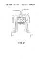
- FIG. 2illustrates a dc magnetron sputtering system adapted for use in the method of the instant invention.
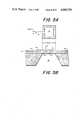
- FIG. 3is a scanning electron microscope photograph of a sputtered ZnO film with its C-axis inclined about 40° with respect to the film normal.
- FIG. 4is a scanning electron microscope photograph of a sputtered AlN film with its C-axis inclined about 30° with respect to the film normal.
- FIGS. 5A and 5Bare a plan view and a cross-sectional elevational view, respectively, of a resonator embodying the instant inventive concept.
- FIG. 6is an impedance plot for the resonator of Example IV.
- FIG. 7is an impedance plot for the resonator of Example V.
- FIG. 8is an impedance plot for the resonator of Example VI.
- FIGS. 9A and 9Bare plots of fundamental frequency as a function of film thickness for ZnO composite resonators and AlN composite resonators, respectively.
- FIGS. 10A and 10Bare plots, for composite resonators comprising piezoelectric material on p+Si membrane, of temperature coefficients of resonance as a function of the ratio of membrane thickness to film thickness for ZnO and AlN, respectively.
- FIGS. 11A and 11Bare graphs comparing temperature coefficient data of composite ZnO/Si and AlN/Si resonators, respectively with the corresponding data of ZnO and AlN plate resonators and AT-cut quartz.
- the instant inventionis a method for depositing thin film piezoelectric material suitable for use as a piezoelectric acoustic shear wave resonator, and a method of making said resonator.
- the resonatorcomprises a piezoelectric electric film of a material having 6 mm symmetry.
- the C-axis of the filmis substantially inclined at an acute angle with respect to the film normal, such that the shear wave coupling coefficient of said film significantly exceeds the longitudinal wave coupling coefficient of said film, whereby the film is capable of shear wave excitation.
- 1A and 1Bare graphs for ZnO and AlN, respectively, showing the shear wave coupling coefficient, K s , and the longitudinal wave coupling coefficient, K 1 , as functions of the C-axis angle of inclination from the film normal.
- the shear wave excitationis at a maximum for both materials when the C-axis angle of inclination is about 40°-50°.
- the filmis sputter deposited in a reactive sputtering system, such as the dc planar magnetron sputtering system illustrated in FIG. 2 or in a dc diode system.
- the reaction chamber 8comprises bell jar 10 containing target 14 and magnet 16 which are cooled by coolant system 18. Gases are provided to reaction chamber 8 by means of inlets 20 and 22.
- Substrate 26is positioned on substrate holder 24 parallel to target 14.
- Substrate holder 24may be heated by means of heater 30 to a temperature monitored by thermocouple 32.
- Chamber 8may be evacuated by conventional means such as a diffusion pump, not shown.
- sputter depositionoccurs when an electric field is applied to chamber 8 such that target 14 serves as a cathode and substrate 26 serves as an anode.
- peripheral control electrode 34to provide an additional dc electric field to chamber 8 during the sputter deposition process.
- the electrodetypically may be a pheripheral ring as shown or it may be a bar-shaped electrode located centrally between the cathode and the anode.
- the electrodeis positioned parallel to and above the plane of the substrate and laterally from directly above the substrate.
- the additional electrical field generated by control electrode 34has the effect of forming a reversal field directly above the substrate which alters the direction of the ion flux as it strikes the substrate causing the film to grow with its crystallographic C-axis preferentially aligned and directed away from control electrode 34.
- the angle of inclination of the C-axisis a function of the voltage of the applied field, the distance of the electrode above the substrate and the lateral distance of the electrode from the substrate.
- the lateral reversal field distanceis 1 to 2, preferably 1 times the distance of the electrode above the plane of the substrate.
- an electrode positioned about 13 mm above the substratewill form a lateral reversal distance of about 25 mm.
- the electrode distance above the substratemay vary from 10 to about 15 mm with the sputtering device described.
- the electrode voltagemay vary from about 30 to 50 volts as measured relative to the substrate.
- the method of the inventionwill produce substrates having a C-axis inclinations up to 45 degrees.
- the anodecollects electron current and thereby prevents arcing to the substrate during deposition.
- Sputtered films for use in shear wave resonatorswhich may be made by the method of the instant invention include piezoelectric materials of 6 mm symmetry such as ZnO and AlN.
- a substrate of (100) Siwas positioned about 5 cm from the target and heated to a temperature of about 300°C.
- the substrate holder on which the substrate was positionedwas substantially parallel to the target.
- the sputter depositiontook place in an atmosphere of 99.999% pure oxygen at a pressure of 0.5-5 millitorr.
- the target cathodewas at a voltage of about -300 volts dc and operated at a current of about 300 milliamperes.
- the peripheral anode voltagewas about 30 volts dc. All voltages were measured relative to the grounded substrate.
- a ZnO filmwas sputter deposited as in Example I except that the substrate was tilted 15° to augment the angle of inclination of the C-axis.
- the C-axis of this filmwas tilted 40° from the film normal, as illustrated in FIG. 3.
- This filmwas clear, transparent and reproducible.
- the film thickness taperwas 0.5% per millimeter and the variation of C-axis inclination angle was about 0.2° per millimeter as estimated from measurements made from the SEM photograph of FIG. 3. These measurements indicate that the film was suitable for use in resonators.
- An AlN filmwas deposited according to the general method used in Example I except that a 99.999% pure Al target and an atmosphere of 99.999% pure nitrogen were used.
- the substrate temperaturewas about 100°C. and the cathode current was about 800 milliamperes.
- the AlN filmgrew at a rate of about 1.5 ⁇ m/hr. When a dc anode voltage of about 30 volts was applied, the film grew with its C-axis tilted at about 30°, as shown in FIG. 4. This angle could be augmented by having the substrate tilted during deposition as described in Example II.
- a substrate of Siwas positioned parallel to and about 5 from the target and heated to a temperature of about 300° C. Sputter deposition took place in an atmosphere of 99.999% pure oxygen at a pressure of 3millitorr.
- the target cathodewas at a voltage of about -550 volts dc at a current of 350 milliamperes.
- the peripheral electrodewas positioned 13 millimeters above the plane of the substrate and the substrate was positioned just inside of the inner periphery of the electrode since the film will not grow in the shadow of the electrode.
- the electrode voltagewas 35 volts dc, relative to ground.
- the C-axis of the filmwas inclined to 45 degrees from the film normal.
- control electrode voltageis generally maintained anywhere between about 20 volts to about 40 volts to promote plasma stability and to obtain better film quality, but the voltage may be lower or higher than this range in order to obtain a lesser or greater angle of inclination of the C-axis.
- Other parameterssuch as target-substrate spacing, substrate temperature and cathode current may be varied as is known in the art of dc magnetron sputtering.
- the substratemay be tilted or not depending on the C-axis angle of inclination desired. In some cases tilting the substrate may cause undesirable variations in film thickness.
- the substratemay comprise, for example, silicon, GaAs, or a combination of silicon and GaAs.
- the substratemay be provided with a deposition layer such as thermally grown oxide, a deposited metal film, or doped p + silicon on which the piezoelectric film is deposited.
- a deposition layersuch as thermally grown oxide, a deposited metal film, or doped p + silicon on which the piezoelectric film is deposited. The orientation of the C-axis of the deposited piezoelectric film appears to be independent of the substrate material and the material of the deposition layer.
- the resonator of the instant inventioncomprises a film of piezoelectric material having its C-axis substantially inclined at an acute angle with respect to the film normal and at least two electrodes in proximity thereto to provide a means of excitation.
- FIGS. 5A and 5BA resonator of the instant invention is illustrated in FIGS. 5A and 5B.
- a substrate 42is provided with a deposition layer 44.
- a film of piezoelectric material 40is sputter deposited by the method of the instant invention onto deposition layer 44. It may be seen that in the absence of deposition layer 44, film 40 may be sputter deposited directly onto substrate 42.
- a generally pyramidal cavity 48is selectively cut into the back side of substrate 42 by known means such as etching.
- FIG. 5Billustrates an embodiment wherein selective etching was used such that layer 44 remained essentially intact, whereby the portion of layer 44 spanning cavity 48 forms a membrane 45.
- the resulting structureis referred to as a composite.
- membrane 45may serve as an electrode.
- that portion of layer 44may also be selectively etched away leaving only a piezoelectric plate spanning cavity 48.
- a conductive layer 50is provided on piezoelectric film 40.
- conductive layer 50may be doped p + silicon or it may be deposited aluminum. The deposition may be done through an aperture as is known in the art so that conductive layer 50 is deposited in the form of an electrode having pad 53 and lead 54.
- conductive layer 50may be deposited over a larger area of film 40 and an electrode may be photolithographically defined therefrom. In either case, electrode pad 53 is opposite cavity 48.
- a conductive layer 52may be provided on the back side of the resonator structure to serve as a second electrode. Conductive layer 52 is opposite electrode pad 53 and may also extend over the back side of substrate 42.
- conductive layer 52may be omitted. In yet another embodiment, conductive layer 52 may be deposited prior to the deposition of piezoelectric film 40 such that conductive layer 52 is between deposition layer 44 and piezoelectric material 40.
- Resonatorscan be characterized in terms of impedance and reasonator Q.
- the impedance Zis determined from the equation ##EQU1## where ⁇ is the reflection coefficient measured as a function of frequency.
- the resonator Qis a measure of the ratio of energy stored to energy lost and is determined from the computed phase of Z, A.sub. ⁇ , such that ##EQU2## where f r is the resonant frequency.
- This definition of Qfollows directly from parallel or series RLC circuits. because impedance is a property of the resonator alone and is not determined by the external circuit, Q determined in this manner is the unloaded or device Q.
- a composite resonatorwas prepared as described above comprising 2.8 ⁇ m ZnO with its C-axis inclined 40° from the film normal on 5 ⁇ m Si having a deposition layer of p + silicon membrane.
- the resonatorwas provided with aluminum electrodes.
- the resonatorwas characterized as having series Q of 4600, parallel Q of 3800, 40 ⁇ series resistance including 10 for metalization, and 495 ⁇ parallel resistance.
- the shear wave resonant responseswere detected at fundamental frequencies of 293.55 MHz for series resonance and 293.66 MHz for parallel resonance. No longitudinal resonant responses were detected.
- FIG. 6shows the phase and absolute value of impedance of the resonator as a function of frequency around fundamental resonance frequencies.
- the temperature coefficient of resonancewas determined by placing the resonator at the end of a coaxial cable in an environmental chamber and measuring the series and parallel resonant frequencies as a function of temperature. The temperature coefficient of resonance was found to be -20.5 ppm/° C. around room temperature.
- a resonatorwas prepared as described in Example V except that prior to deposition of the electrodes the p + silicon membrane was removed from under the ZnO using CF 4 gas plasma etching, leaving a ZnO plate supported at its periphery.
- the ZnO plateis mechanically rugged and may be made as thin as 1 ⁇ m, although plate bowing was obsereved if the plate thickness was less than 3 ⁇ m.
- the shear wave resonant responseswere measured at fundamental frequencies of 398.96 MHz for series resonance and 403.60 MHz for parallel resonance which corresponds to a shear acoustic wave velocity of 2830 m/s.
- a 3.8 ⁇ m thick AlN plate resonatorwas prepared as generally described in Example VI.
- the AlN platewas even more rugged than the ZnO plate.
- the fundamental shear wave resonant responsewas measured at 734.45 MHz, corresponding to a shear acoustic wave velocity of 5585 m/s.
- the resonator Qwas lower than expected due to a parasitic transducer effect.
- the impedance plot for this resonatoris shown in FIG. 8.
- resonator frequencyis a function of the film thickness and the type of film material used. In a composite resonator, the membrane material and thickness is also a factor.
- FIGS. 9A and 9Bshow fundamental parallel resonant frequencies of composite resonators having a p + silicon membrane as a function of p + silicon membrane thickness for several values of ZnO or AlN thickness.
- ZnO composite resonatorshave fundamental resonant frequencies in the range of 200 MHz to 400 MHz, while the frequencies of AlN composite resonators range from 300 MHz to 500 MHz.
- resonatorsFor many applications it would be desirable to have resonators whose response is relatively constant over a range of operating temperatures. Ideally, the resonators would have a temperature coefficient of resonance of 0 ppm/C°.
- a unique advantage of the instant inventionis that shear wave resonators can be made which approach this condition.
- FIGS. 10A and 10Bare plots of temperature coefficients as a function of these ratios for ZnO and AlN, respectively.
- the solid linesare the predictions of linear elastic theory, and the points are experimental data taken near room temperature by the general method described in Example V.
- FIGS. 11A and 11Bare graphs comparing temperature coefficient data of composite p + Si/ZnO and p + Si/AlN resonators, respectively, with the corresponding data of ZnO and AlN plate resonators and AT-cut quartz, a material commonly used in mechanical plate resonators.
- the ZnO composite resonatorcomprised 0.85 ⁇ m ZnO on 8 ⁇ m p + Si
- the AlN resonatorcomprised 2.0 ⁇ m AlN on 6.3 ⁇ um p + Si. It may be seen that the composite resonators of the instant invention have temperature coefficients better than AT-cut quartz.
Landscapes
- Chemical & Material Sciences (AREA)
- Engineering & Computer Science (AREA)
- Chemical Kinetics & Catalysis (AREA)
- Materials Engineering (AREA)
- Mechanical Engineering (AREA)
- Metallurgy (AREA)
- Organic Chemistry (AREA)
- Manufacturing & Machinery (AREA)
- Physics & Mathematics (AREA)
- Plasma & Fusion (AREA)
- Analytical Chemistry (AREA)
- Piezo-Electric Or Mechanical Vibrators, Or Delay Or Filter Circuits (AREA)
Abstract
Description
Claims (13)
Priority Applications (2)
| Application Number | Priority Date | Filing Date | Title |
|---|---|---|---|
| US06/736,164US4640756A (en) | 1983-10-25 | 1985-05-20 | Method of making a piezoelectric shear wave resonator |
| US06/913,192US4719383A (en) | 1985-05-20 | 1986-09-30 | Piezoelectric shear wave resonator and method of making same |
Applications Claiming Priority (2)
| Application Number | Priority Date | Filing Date | Title |
|---|---|---|---|
| US54541183A | 1983-10-25 | 1983-10-25 | |
| US06/736,164US4640756A (en) | 1983-10-25 | 1985-05-20 | Method of making a piezoelectric shear wave resonator |
Related Parent Applications (1)
| Application Number | Title | Priority Date | Filing Date |
|---|---|---|---|
| US54541183AContinuation-In-Part | 1983-10-25 | 1983-10-25 |
Related Child Applications (1)
| Application Number | Title | Priority Date | Filing Date |
|---|---|---|---|
| US06/913,192DivisionUS4719383A (en) | 1985-05-20 | 1986-09-30 | Piezoelectric shear wave resonator and method of making same |
Publications (1)
| Publication Number | Publication Date |
|---|---|
| US4640756Atrue US4640756A (en) | 1987-02-03 |
Family
ID=27067928
Family Applications (1)
| Application Number | Title | Priority Date | Filing Date |
|---|---|---|---|
| US06/736,164Expired - LifetimeUS4640756A (en) | 1983-10-25 | 1985-05-20 | Method of making a piezoelectric shear wave resonator |
Country Status (1)
| Country | Link |
|---|---|
| US (1) | US4640756A (en) |
Cited By (91)
| Publication number | Priority date | Publication date | Assignee | Title |
|---|---|---|---|---|
| US5059847A (en)* | 1989-04-11 | 1991-10-22 | Sanyo Electric Co., Ltd. | Surface acoustic wave device |
| US5231327A (en)* | 1990-12-14 | 1993-07-27 | Tfr Technologies, Inc. | Optimized piezoelectric resonator-based networks |
| US5232571A (en)* | 1991-12-23 | 1993-08-03 | Iowa State University Research Foundation, Inc. | Aluminum nitride deposition using an AlN/Al sputter cycle technique |
| US5498920A (en)* | 1993-05-18 | 1996-03-12 | Sanyo Electric Co., Ltd. | Acoustic wave device and process for producing same |
| US5596239A (en)* | 1995-06-29 | 1997-01-21 | Motorola, Inc. | Enhanced quality factor resonator |
| US5617065A (en)* | 1995-06-29 | 1997-04-01 | Motorola, Inc. | Filter using enhanced quality factor resonator and method |
| EP0771070A3 (en)* | 1995-10-27 | 1997-07-02 | Mitsubishi Electric Corp | Thin film and volume acoustic wave device |
| EP0795953A1 (en)* | 1996-03-15 | 1997-09-17 | Centre Electronique Horloger S.A. | Electronic device comprising an integrated time base |
| US5696423A (en)* | 1995-06-29 | 1997-12-09 | Motorola, Inc. | Temperature compenated resonator and method |
| US5789845A (en)* | 1994-11-24 | 1998-08-04 | Mitsubishi Denki Kabushiki Kaisha | Film bulk acoustic wave device |
| US6746577B1 (en)* | 1999-12-16 | 2004-06-08 | Agere Systems, Inc. | Method and apparatus for thickness control and reproducibility of dielectric film deposition |
| US20060132262A1 (en)* | 2004-12-22 | 2006-06-22 | Fazzio Ronald S | Acoustic resonator performance enhancement using selective metal etch |
| US20060197411A1 (en)* | 2005-03-04 | 2006-09-07 | Hoen Storrs T | Film-bulk acoustic wave resonator with motion plate |
| US20070063622A1 (en)* | 2005-09-09 | 2007-03-22 | Rudy Richard C | Adjusted frequency temperature coefficient resonator |
| US20070086080A1 (en)* | 2005-10-18 | 2007-04-19 | Larson John D Iii | Acoustic galvanic isolator incorporating series-connected decoupled stacked bulk acoustic resonators |
| US20070086274A1 (en)* | 2005-10-18 | 2007-04-19 | Ken Nishimura | Acoustically communicating data signals across an electrical isolation barrier |
| US20070090892A1 (en)* | 2005-10-18 | 2007-04-26 | Larson John D Iii | Acoustic galvanic isolator incorporating single decoupled stacked bulk acoustic resonator |
| US20070120625A1 (en)* | 2005-11-30 | 2007-05-31 | Larson John D Iii | Film bulk acoustic resonator (FBAR) devices with temperature compensation |
| US20070176710A1 (en)* | 2006-01-30 | 2007-08-02 | Tiberiu Jamneala | Impedance transforming bulk acoustic wave baluns |
| DE102006003847A1 (en)* | 2006-01-26 | 2007-08-09 | Siemens Ag | Method and apparatus for producing a polycrystalline ceramic film on a substrate, capacitor structure with the ceramic film and use of the capacitor structure |
| US20070205850A1 (en)* | 2004-11-15 | 2007-09-06 | Tiberiu Jamneala | Piezoelectric resonator structures and electrical filters having frame elements |
| US20070210748A1 (en)* | 2006-03-09 | 2007-09-13 | Mark Unkrich | Power supply and electronic device having integrated power supply |
| US20070210724A1 (en)* | 2006-03-09 | 2007-09-13 | Mark Unkrich | Power adapter and DC-DC converter having acoustic transformer |
| US20070236310A1 (en)* | 2006-03-10 | 2007-10-11 | Fazzio R S | Electronic device on substrate with cavity and mitigated parasitic leakage path |
| US20070279153A1 (en)* | 2006-05-31 | 2007-12-06 | Ruby Richard C | Piezoelectric resonator structures and electrical filters |
| US20080079516A1 (en)* | 2006-09-28 | 2008-04-03 | Ruby Richard C | HBAR oscillator and method of manufacture |
| US20080202239A1 (en)* | 2007-02-28 | 2008-08-28 | Fazzio R Shane | Piezoelectric acceleration sensor |
| US7425787B2 (en) | 2005-10-18 | 2008-09-16 | Avago Technologies Wireless Ip (Singapore) Pte. Ltd. | Acoustic galvanic isolator incorporating single insulated decoupled stacked bulk acoustic resonator with acoustically-resonant electrical insulator |
| US20080258842A1 (en)* | 2004-10-01 | 2008-10-23 | Avago Technologies Wireless Ip (Singapore) Pte. Ltd. | Acoustic resonator performance enhancement using alternating frame structure |
| US20080285165A1 (en)* | 2007-05-14 | 2008-11-20 | Wu Kuohua Angus | Thin film filter system and method |
| US20090025207A1 (en)* | 2005-04-29 | 2009-01-29 | Cardiac Pacemakers, Inc. | Method and apparatus for an implantable pulse generator with a stacked battery and capacitor |
| US20090073730A1 (en)* | 2005-10-31 | 2009-03-19 | Avago Technologies Wireless Ip (Singapore) Pte. Ltd. | AC-DC Power Converter |
| US20090086654A1 (en)* | 2007-09-28 | 2009-04-02 | Tiberiu Jamneala | Single stack coupled resonators having differential output |
| US20090096547A1 (en)* | 2005-04-18 | 2009-04-16 | Avago Technologies Wireless Ip(Singapore) Pte.Ltd. | Acoustically coupled resonators and method of making the same |
| US20090273415A1 (en)* | 2008-04-30 | 2009-11-05 | Avago Technologies Wireless Ip (Singapore) Pte. Ltd. | Bulk acoustic resonator electrical impedance transformers |
| US20090273256A1 (en)* | 2008-04-30 | 2009-11-05 | Avago Technologies Wireless Ip (Singapore) Pte. Ltd. | Transceiver circuit for film bulk acoustic resonator (fbar) transducers |
| US7615833B2 (en) | 2004-07-13 | 2009-11-10 | Avago Technologies Wireless Ip (Singapore) Pte. Ltd. | Film bulk acoustic resonator package and method of fabricating same |
| US20100133091A1 (en)* | 2006-11-27 | 2010-06-03 | Omron Corporation | Thin film producing method and hexagonal piezoelectric thin film produced thereby |
| US20100142098A1 (en)* | 2008-12-09 | 2010-06-10 | Tdk Corporation | Method for manufacturing magnetoresistance effect element using simultaneous sputtering of Zn and ZnO |
| US7746677B2 (en) | 2006-03-09 | 2010-06-29 | Avago Technologies Wireless Ip (Singapore) Pte. Ltd. | AC-DC converter circuit and power supply |
| US7802349B2 (en) | 2003-03-07 | 2010-09-28 | Avago Technologies Wireless Ip (Singapore) Pte. Ltd. | Manufacturing process for thin film bulk acoustic resonator (FBAR) filters |
| US20100327994A1 (en)* | 2009-06-24 | 2010-12-30 | Avago Technologies Wireless Ip (Singapore) Pte. Ltd. | Acoustic resonator structure having an electrode with a cantilevered portion |
| US20100327697A1 (en)* | 2009-06-24 | 2010-12-30 | Avago Technologies Wireless Ip (Singapore) Pte. Ltd. | Acoustic resonator structure comprising a bridge |
| US20110128092A1 (en)* | 2009-11-30 | 2011-06-02 | Avago Technologies Wireless Ip (Singapore) Pte. Ltd. | Duplexer with negative phase shifting circuit |
| US8143082B2 (en) | 2004-12-15 | 2012-03-27 | Avago Technologies Wireless Ip (Singapore) Pte. Ltd. | Wafer bonding of micro-electro mechanical systems to active circuitry |
| US20120187804A1 (en)* | 2011-01-25 | 2012-07-26 | Gibbons Brady J | Architecture for piezoelectric mems devices |
| US8230562B2 (en) | 2005-04-06 | 2012-07-31 | Avago Technologies Wireless Ip (Singapore) Pte. Ltd. | Method of fabricating an acoustic resonator comprising a filled recessed region |
| US8350445B1 (en) | 2011-06-16 | 2013-01-08 | Avago Technologies Wireless Ip (Singapore) Pte. Ltd. | Bulk acoustic resonator comprising non-piezoelectric layer and bridge |
| US8575820B2 (en) | 2011-03-29 | 2013-11-05 | Avago Technologies General Ip (Singapore) Pte. Ltd. | Stacked bulk acoustic resonator |
| US8796904B2 (en) | 2011-10-31 | 2014-08-05 | Avago Technologies General Ip (Singapore) Pte. Ltd. | Bulk acoustic resonator comprising piezoelectric layer and inverse piezoelectric layer |
| US8922302B2 (en) | 2011-08-24 | 2014-12-30 | Avago Technologies General Ip (Singapore) Pte. Ltd. | Acoustic resonator formed on a pedestal |
| US8962443B2 (en) | 2011-01-31 | 2015-02-24 | Avago Technologies General Ip (Singapore) Pte. Ltd. | Semiconductor device having an airbridge and method of fabricating the same |
| US9048812B2 (en) | 2011-02-28 | 2015-06-02 | Avago Technologies General Ip (Singapore) Pte. Ltd. | Bulk acoustic wave resonator comprising bridge formed within piezoelectric layer |
| US9083302B2 (en) | 2011-02-28 | 2015-07-14 | Avago Technologies General Ip (Singapore) Pte. Ltd. | Stacked bulk acoustic resonator comprising a bridge and an acoustic reflector along a perimeter of the resonator |
| US9136818B2 (en) | 2011-02-28 | 2015-09-15 | Avago Technologies General Ip (Singapore) Pte. Ltd. | Stacked acoustic resonator comprising a bridge |
| US9148117B2 (en) | 2011-02-28 | 2015-09-29 | Avago Technologies General Ip (Singapore) Pte. Ltd. | Coupled resonator filter comprising a bridge and frame elements |
| US9154112B2 (en) | 2011-02-28 | 2015-10-06 | Avago Technologies General Ip (Singapore) Pte. Ltd. | Coupled resonator filter comprising a bridge |
| US9203374B2 (en) | 2011-02-28 | 2015-12-01 | Avago Technologies General Ip (Singapore) Pte. Ltd. | Film bulk acoustic resonator comprising a bridge |
| US9243316B2 (en) | 2010-01-22 | 2016-01-26 | Avago Technologies General Ip (Singapore) Pte. Ltd. | Method of fabricating piezoelectric material with selected c-axis orientation |
| US9425764B2 (en) | 2012-10-25 | 2016-08-23 | Avago Technologies General Ip (Singapore) Pte. Ltd. | Accoustic resonator having composite electrodes with integrated lateral features |
| US9444426B2 (en) | 2012-10-25 | 2016-09-13 | Avago Technologies General Ip (Singapore) Pte. Ltd. | Accoustic resonator having integrated lateral feature and temperature compensation feature |
| WO2017066449A1 (en)* | 2015-10-14 | 2017-04-20 | Qorvo Us, Inc. | Multi-stage deposition system for growth of inclined c-axis piezoelectric material structures |
| WO2017070177A1 (en)* | 2015-10-21 | 2017-04-27 | Qorvo Us, Inc. | Resonator structure with enhanced reflection of shear and longitudinal modes of acoustic vibrations |
| WO2017075344A1 (en) | 2015-10-28 | 2017-05-04 | Qorvo Us, Inc. | Sensor device with baw resonator and through-substrate fluidic vias |
| US20170122911A1 (en)* | 2015-10-30 | 2017-05-04 | Qorvo Us, Inc. | Multi-frequency baw mixing and sensing system and method |
| WO2017078992A1 (en) | 2015-11-06 | 2017-05-11 | Qorvo Us, Inc. | Acoustic resonator devices and fabrication methods providing hermeticity and surface functionalization |
| US20170134002A1 (en)* | 2015-11-09 | 2017-05-11 | Qorvo Us, Inc. | Baw sensor with enhanced surface area active region |
| US20170261503A1 (en)* | 2016-03-11 | 2017-09-14 | Qorvo Us, Inc. | Baw sensor fluidic device with increased dynamic measurement range |
| US20180019728A1 (en)* | 2016-07-12 | 2018-01-18 | Murata Manufacturing Co., Ltd. | Piezoelectric mems resonator with a high quality factor |
| WO2018031055A1 (en) | 2016-08-11 | 2018-02-15 | Qorvo Us, Inc. | Acoustic resonator device with controlled placement of functionalization material |
| US10267770B2 (en) | 2016-07-27 | 2019-04-23 | Qorvo Us, Inc. | Acoustic resonator devices and methods with noble metal layer for functionalization |
| US10326425B2 (en) | 2015-11-20 | 2019-06-18 | Qorvo Us, Inc. | Acoustic resonator with reduced mechanical clamping of an active region for enhanced shear mode response |
| US10330643B2 (en) | 2016-02-04 | 2019-06-25 | Qorvo Us, Inc. | BAW sensing and filtration device and related methods |
| US10330642B2 (en)* | 2015-12-14 | 2019-06-25 | Qorvo Us, Inc. | BAW sensor device with peel-resistant wall structure |
| US10352904B2 (en) | 2015-10-26 | 2019-07-16 | Qorvo Us, Inc. | Acoustic resonator devices and methods providing patterned functionalization areas |
| US10371667B2 (en) | 2015-11-16 | 2019-08-06 | Qorvo Us, Inc. | BAW sensor with passive mixing structures |
| US10458982B2 (en) | 2015-10-30 | 2019-10-29 | Qorvo Us, Inc. | Fluidic device including BAW resonators along opposing channel surfaces |
| WO2020010347A1 (en) | 2018-07-06 | 2020-01-09 | Qorvo Us, Inc. | Sensor with droplet retaining structure |
| US10533972B2 (en) | 2015-11-02 | 2020-01-14 | Qorvo Us, Inc. | Fluidic device with fluid port orthogonal to functionalized active region |
| US10571437B2 (en) | 2015-12-15 | 2020-02-25 | Qorvo Us, Inc. | Temperature compensation and operational configuration for bulk acoustic wave resonator devices |
| US10659000B2 (en) | 2016-03-25 | 2020-05-19 | Qorvo Biotechnologies, Llc | Fluidic sensor device having UV-blocking cover |
| WO2020227396A1 (en) | 2019-05-06 | 2020-11-12 | Qorvo Biotechnologies, Llc | Acoustic resonator device |
| US11209394B2 (en) | 2016-07-26 | 2021-12-28 | Qorvo Us, Inc. | Cartridges for integrated BAW biosensors and methods for using the same |
| US11223342B2 (en) | 2016-12-07 | 2022-01-11 | Qorvo Us, Inc. | Bulk acoustic wave sensor having an overmoded resonating structure |
| US11325121B2 (en) | 2019-03-29 | 2022-05-10 | Qorvo Us, Inc. | Analyte depletion for sensor equilibration |
| US11381212B2 (en)* | 2018-03-21 | 2022-07-05 | Qorvo Us, Inc. | Piezoelectric bulk layers with tilted c-axis orientation and methods for making the same |
| US11401601B2 (en) | 2019-09-13 | 2022-08-02 | Qorvo Us, Inc. | Piezoelectric bulk layers with tilted c-axis orientation and methods for making the same |
| US11467126B2 (en) | 2016-07-29 | 2022-10-11 | Qorvo Us, Inc. | BAW biosensor including heater and temperature sensor and methods for using the same |
| US11824511B2 (en) | 2018-03-21 | 2023-11-21 | Qorvo Us, Inc. | Method for manufacturing piezoelectric bulk layers with tilted c-axis orientation |
| US11940414B2 (en) | 2019-03-29 | 2024-03-26 | Zomedica Biotechnologies Llc | Crowded sensor |
| US12360125B2 (en) | 2016-07-25 | 2025-07-15 | Zomedica Biotechnologies Llc | Biosensor for coagulation testing |
Citations (9)
| Publication number | Priority date | Publication date | Assignee | Title |
|---|---|---|---|---|
| US3486046A (en)* | 1968-10-17 | 1969-12-23 | Westinghouse Electric Corp | Thin film piezoelectric resonator |
| US3558351A (en)* | 1968-12-19 | 1971-01-26 | Bell Telephone Labor Inc | Thin semiconductor films |
| US3573960A (en)* | 1968-12-19 | 1971-04-06 | Bell Telephone Labor Inc | Torsional mode elastic wave transducers |
| US3766041A (en)* | 1970-09-29 | 1973-10-16 | Matsushita Electric Industrial Co Ltd | Method of producing piezoelectric thin films by cathodic sputtering |
| US3846649A (en)* | 1973-06-18 | 1974-11-05 | Rca Corp | Piezoelectric transducer comprising oriented zinc oxide film and method of manufacture |
| US4142124A (en)* | 1977-01-25 | 1979-02-27 | Murata Manufacturing Co., Ltd. | Piezoelectric crystalline ZnO with 0.01 to 20.0 atomic % Mn |
| US4164676A (en)* | 1977-07-28 | 1979-08-14 | Murata Manufacturing Co., Ltd. | Piezoelectric crystalline film of zinc oxide containing additive elements |
| US4229506A (en)* | 1977-09-17 | 1980-10-21 | Murata Manufacturing Co., Ltd. | Piezoelectric crystalline film of zinc oxide and method for making same |
| US4297189A (en)* | 1980-06-27 | 1981-10-27 | Rockwell International Corporation | Deposition of ordered crystalline films |
- 1985
- 1985-05-20USUS06/736,164patent/US4640756A/ennot_activeExpired - Lifetime
Patent Citations (9)
| Publication number | Priority date | Publication date | Assignee | Title |
|---|---|---|---|---|
| US3486046A (en)* | 1968-10-17 | 1969-12-23 | Westinghouse Electric Corp | Thin film piezoelectric resonator |
| US3558351A (en)* | 1968-12-19 | 1971-01-26 | Bell Telephone Labor Inc | Thin semiconductor films |
| US3573960A (en)* | 1968-12-19 | 1971-04-06 | Bell Telephone Labor Inc | Torsional mode elastic wave transducers |
| US3766041A (en)* | 1970-09-29 | 1973-10-16 | Matsushita Electric Industrial Co Ltd | Method of producing piezoelectric thin films by cathodic sputtering |
| US3846649A (en)* | 1973-06-18 | 1974-11-05 | Rca Corp | Piezoelectric transducer comprising oriented zinc oxide film and method of manufacture |
| US4142124A (en)* | 1977-01-25 | 1979-02-27 | Murata Manufacturing Co., Ltd. | Piezoelectric crystalline ZnO with 0.01 to 20.0 atomic % Mn |
| US4164676A (en)* | 1977-07-28 | 1979-08-14 | Murata Manufacturing Co., Ltd. | Piezoelectric crystalline film of zinc oxide containing additive elements |
| US4229506A (en)* | 1977-09-17 | 1980-10-21 | Murata Manufacturing Co., Ltd. | Piezoelectric crystalline film of zinc oxide and method for making same |
| US4297189A (en)* | 1980-06-27 | 1981-10-27 | Rockwell International Corporation | Deposition of ordered crystalline films |
Non-Patent Citations (22)
| Title |
|---|
| "Acoustic Bulk Wave Composite Reactors", Lakin et al, Appl. Phys. Lett., 38 (3), p. 125, 2/1/81. |
| "Aluminum Nitride Thin Film and Composite Bulk Wave Resonators", Lakin et al., 36th Annual Frequency Control Symposium, 1982. |
| "Cadmium Sulphide and Zinc Oxide Thin-Film Transducers", Foster et al., IEEE Transactions on Sonics and Ultrasonics, vol. SU-15, No. 1, p. 28. |
| "C-Axis Inclined ZnO Piezoelectric Shear Wave Films", Wang et al., App. Phys. Lett., 42 (4), 2/15/83. |
| "Highly Oriented ZnO Films by RF Sputtering of Hemispherical Electrode System", Ohji et al., J. App. Phys., vol. 47, No. 4, Apr., 1976. |
| "Low-Temperature Coefficient Bulk Acoustic Wave Composite Resonators", Wang et al., Appl. Phys. Lett., 40 (4), p. 308, 2/15/82. |
| "Sputtered C-Axis Inclined Piezoelectric Films and Shear Wave Resonators", Wang et al., 37th Annual Symposium on Frequency Control, 1983. |
| "Sputtered C-Axis Inclined ZnO Films for Shear Wave Resonators", Wang et al., 1982 Ultrasonics Symposium. |
| "Thin Film Resonators and Filters", Lakin et al., 1982 Ultrasonics Symposium. |
| "UHF Composite Bulk Wave Resonators", Lakin et al, 1980 IEEE Ultrasonics Symposium, p. 834. |
| "Variation of C-Axis Orientation of ZnO Thin Films Deposited by DC Diode Sputtering", Minikata et al., J. Appl. Phys., vol. 12, No. 3, p. 474. |
| Acoustic Bulk Wave Composite Reactors , Lakin et al, Appl. Phys. Lett., 38 (3), p. 125, 2/1/81.* |
| Aluminum Nitride Thin Film and Composite Bulk Wave Resonators , Lakin et al., 36th Annual Frequency Control Symposium, 1982.* |
| C Axis Inclined ZnO Piezoelectric Shear Wave Films , Wang et al., App. Phys. Lett., 42 (4), 2/15/83.* |
| Cadmium Sulphide and Zinc Oxide Thin Film Transducers , Foster et al., IEEE Transactions on Sonics and Ultrasonics, vol. SU 15, No. 1, p. 28.* |
| Highly Oriented ZnO Films by RF Sputtering of Hemispherical Electrode System , Ohji et al., J. App. Phys., vol. 47, No. 4, Apr., 1976.* |
| Low Temperature Coefficient Bulk Acoustic Wave Composite Resonators , Wang et al., Appl. Phys. Lett., 40 (4), p. 308, 2/15/82.* |
| Sputtered C Axis Inclined Piezoelectric Films and Shear Wave Resonators , Wang et al., 37th Annual Symposium on Frequency Control, 1983.* |
| Sputtered C Axis Inclined ZnO Films for Shear Wave Resonators , Wang et al., 1982 Ultrasonics Symposium.* |
| Thin Film Resonators and Filters , Lakin et al., 1982 Ultrasonics Symposium.* |
| UHF Composite Bulk Wave Resonators , Lakin et al, 1980 IEEE Ultrasonics Symposium, p. 834.* |
| Variation of C Axis Orientation of ZnO Thin Films Deposited by DC Diode Sputtering , Minikata et al., J. Appl. Phys., vol. 12, No. 3, p. 474.* |
Cited By (165)
| Publication number | Priority date | Publication date | Assignee | Title |
|---|---|---|---|---|
| US5059847A (en)* | 1989-04-11 | 1991-10-22 | Sanyo Electric Co., Ltd. | Surface acoustic wave device |
| US5231327A (en)* | 1990-12-14 | 1993-07-27 | Tfr Technologies, Inc. | Optimized piezoelectric resonator-based networks |
| US5404628A (en)* | 1990-12-14 | 1995-04-11 | Tfr Technologies, Inc. | Method for optimizing piezoelectric resonator-based networks |
| US5232571A (en)* | 1991-12-23 | 1993-08-03 | Iowa State University Research Foundation, Inc. | Aluminum nitride deposition using an AlN/Al sputter cycle technique |
| US5498920A (en)* | 1993-05-18 | 1996-03-12 | Sanyo Electric Co., Ltd. | Acoustic wave device and process for producing same |
| US5789845A (en)* | 1994-11-24 | 1998-08-04 | Mitsubishi Denki Kabushiki Kaisha | Film bulk acoustic wave device |
| US5617065A (en)* | 1995-06-29 | 1997-04-01 | Motorola, Inc. | Filter using enhanced quality factor resonator and method |
| US5884378A (en)* | 1995-06-29 | 1999-03-23 | Motorola, Inc. | Method of making an enhanced quality factor resonator |
| US5696423A (en)* | 1995-06-29 | 1997-12-09 | Motorola, Inc. | Temperature compenated resonator and method |
| US5596239A (en)* | 1995-06-29 | 1997-01-21 | Motorola, Inc. | Enhanced quality factor resonator |
| US6131256A (en)* | 1995-06-29 | 2000-10-17 | Motorola, Inc. | Temperature compensated resonator and method |
| EP0771070A3 (en)* | 1995-10-27 | 1997-07-02 | Mitsubishi Electric Corp | Thin film and volume acoustic wave device |
| JP3371050B2 (en) | 1995-10-27 | 2003-01-27 | 三菱電機株式会社 | Thin film piezoelectric element |
| EP0795953A1 (en)* | 1996-03-15 | 1997-09-17 | Centre Electronique Horloger S.A. | Electronic device comprising an integrated time base |
| FR2746229A1 (en)* | 1996-03-15 | 1997-09-19 | Centre Electron Horloger | ELECTRONIC DEVICE COMPRISING AN INTEGRATED TIME BASE |
| US5856765A (en)* | 1996-03-15 | 1999-01-05 | Centre Electronique Horloger S.A. | Electronic device comprising an integrated time base |
| US6746577B1 (en)* | 1999-12-16 | 2004-06-08 | Agere Systems, Inc. | Method and apparatus for thickness control and reproducibility of dielectric film deposition |
| US7802349B2 (en) | 2003-03-07 | 2010-09-28 | Avago Technologies Wireless Ip (Singapore) Pte. Ltd. | Manufacturing process for thin film bulk acoustic resonator (FBAR) filters |
| US7615833B2 (en) | 2004-07-13 | 2009-11-10 | Avago Technologies Wireless Ip (Singapore) Pte. Ltd. | Film bulk acoustic resonator package and method of fabricating same |
| US20080258842A1 (en)* | 2004-10-01 | 2008-10-23 | Avago Technologies Wireless Ip (Singapore) Pte. Ltd. | Acoustic resonator performance enhancement using alternating frame structure |
| US7714684B2 (en) | 2004-10-01 | 2010-05-11 | Avago Technologies Wireless Ip (Singapore) Pte. Ltd. | Acoustic resonator performance enhancement using alternating frame structure |
| US8981876B2 (en) | 2004-11-15 | 2015-03-17 | Avago Technologies General Ip (Singapore) Pte. Ltd. | Piezoelectric resonator structures and electrical filters having frame elements |
| US20070205850A1 (en)* | 2004-11-15 | 2007-09-06 | Tiberiu Jamneala | Piezoelectric resonator structures and electrical filters having frame elements |
| US8143082B2 (en) | 2004-12-15 | 2012-03-27 | Avago Technologies Wireless Ip (Singapore) Pte. Ltd. | Wafer bonding of micro-electro mechanical systems to active circuitry |
| US7791434B2 (en) | 2004-12-22 | 2010-09-07 | Avago Technologies Wireless Ip (Singapore) Pte. Ltd. | Acoustic resonator performance enhancement using selective metal etch and having a trench in the piezoelectric |
| US20060132262A1 (en)* | 2004-12-22 | 2006-06-22 | Fazzio Ronald S | Acoustic resonator performance enhancement using selective metal etch |
| US8188810B2 (en) | 2004-12-22 | 2012-05-29 | Avago Technologies Wireless Ip (Singapore) Pte. Ltd. | Acoustic resonator performance enhancement using selective metal etch |
| US20060197411A1 (en)* | 2005-03-04 | 2006-09-07 | Hoen Storrs T | Film-bulk acoustic wave resonator with motion plate |
| US7427819B2 (en) | 2005-03-04 | 2008-09-23 | Avago Wireless Ip Pte Ltd | Film-bulk acoustic wave resonator with motion plate and method |
| US8230562B2 (en) | 2005-04-06 | 2012-07-31 | Avago Technologies Wireless Ip (Singapore) Pte. Ltd. | Method of fabricating an acoustic resonator comprising a filled recessed region |
| US20090096547A1 (en)* | 2005-04-18 | 2009-04-16 | Avago Technologies Wireless Ip(Singapore) Pte.Ltd. | Acoustically coupled resonators and method of making the same |
| US20090025207A1 (en)* | 2005-04-29 | 2009-01-29 | Cardiac Pacemakers, Inc. | Method and apparatus for an implantable pulse generator with a stacked battery and capacitor |
| US20070063622A1 (en)* | 2005-09-09 | 2007-03-22 | Rudy Richard C | Adjusted frequency temperature coefficient resonator |
| US7868522B2 (en) | 2005-09-09 | 2011-01-11 | Avago Technologies Wireless Ip (Singapore) Pte. Ltd. | Adjusted frequency temperature coefficient resonator |
| US20070086080A1 (en)* | 2005-10-18 | 2007-04-19 | Larson John D Iii | Acoustic galvanic isolator incorporating series-connected decoupled stacked bulk acoustic resonators |
| US7425787B2 (en) | 2005-10-18 | 2008-09-16 | Avago Technologies Wireless Ip (Singapore) Pte. Ltd. | Acoustic galvanic isolator incorporating single insulated decoupled stacked bulk acoustic resonator with acoustically-resonant electrical insulator |
| US7737807B2 (en) | 2005-10-18 | 2010-06-15 | Avago Technologies Wireless Ip (Singapore) Pte. Ltd. | Acoustic galvanic isolator incorporating series-connected decoupled stacked bulk acoustic resonators |
| US7675390B2 (en) | 2005-10-18 | 2010-03-09 | Avago Technologies Wireless Ip (Singapore) Pte. Ltd. | Acoustic galvanic isolator incorporating single decoupled stacked bulk acoustic resonator |
| US20070090892A1 (en)* | 2005-10-18 | 2007-04-26 | Larson John D Iii | Acoustic galvanic isolator incorporating single decoupled stacked bulk acoustic resonator |
| US20070086274A1 (en)* | 2005-10-18 | 2007-04-19 | Ken Nishimura | Acoustically communicating data signals across an electrical isolation barrier |
| US7525398B2 (en) | 2005-10-18 | 2009-04-28 | Avago Technologies General Ip (Singapore) Pte. Ltd. | Acoustically communicating data signals across an electrical isolation barrier |
| US7852644B2 (en) | 2005-10-31 | 2010-12-14 | Avago Technologies General Ip (Singapore) Pte. Ltd. | AC-DC power converter |
| US20090073730A1 (en)* | 2005-10-31 | 2009-03-19 | Avago Technologies Wireless Ip (Singapore) Pte. Ltd. | AC-DC Power Converter |
| US7561009B2 (en) | 2005-11-30 | 2009-07-14 | Avago Technologies General Ip (Singapore) Pte. Ltd. | Film bulk acoustic resonator (FBAR) devices with temperature compensation |
| US20070120625A1 (en)* | 2005-11-30 | 2007-05-31 | Larson John D Iii | Film bulk acoustic resonator (FBAR) devices with temperature compensation |
| GB2432980A (en)* | 2005-11-30 | 2007-06-06 | Agilent Technologies Inc | Film bulk acoustic resonator (FBAR) devices with temperature compensation layers |
| GB2432980B (en)* | 2005-11-30 | 2010-12-15 | Agilent Technologies Inc | Film bulk acoustic resonator (FBAR) devices with temperature compensation |
| DE102006003847B4 (en)* | 2006-01-26 | 2011-08-18 | Siemens AG, 80333 | Method and apparatus for producing a polycrystalline ceramic film on a substrate |
| DE102006003847A1 (en)* | 2006-01-26 | 2007-08-09 | Siemens Ag | Method and apparatus for producing a polycrystalline ceramic film on a substrate, capacitor structure with the ceramic film and use of the capacitor structure |
| US8491957B2 (en) | 2006-01-26 | 2013-07-23 | Siemens Aktiengesellschaft | Method for producing a polycrystalline ceramic film on a substrate using a shutter |
| US7612636B2 (en) | 2006-01-30 | 2009-11-03 | Avago Technologies Wireless Ip (Singapore) Pte. Ltd. | Impedance transforming bulk acoustic wave baluns |
| US20070176710A1 (en)* | 2006-01-30 | 2007-08-02 | Tiberiu Jamneala | Impedance transforming bulk acoustic wave baluns |
| US20100202174A1 (en)* | 2006-03-09 | 2010-08-12 | Avago Technologies Wireless Ip (Singapore) Pte. Ltd. | Ac-dc converter circuit and power supply |
| US8238129B2 (en) | 2006-03-09 | 2012-08-07 | Avago Technologies Wireless Ip (Singapore) Pte. Ltd. | AC-DC converter circuit and power supply |
| US20070210724A1 (en)* | 2006-03-09 | 2007-09-13 | Mark Unkrich | Power adapter and DC-DC converter having acoustic transformer |
| US20070210748A1 (en)* | 2006-03-09 | 2007-09-13 | Mark Unkrich | Power supply and electronic device having integrated power supply |
| US7746677B2 (en) | 2006-03-09 | 2010-06-29 | Avago Technologies Wireless Ip (Singapore) Pte. Ltd. | AC-DC converter circuit and power supply |
| US7479685B2 (en) | 2006-03-10 | 2009-01-20 | Avago Technologies General Ip (Singapore) Pte. Ltd. | Electronic device on substrate with cavity and mitigated parasitic leakage path |
| US20090101999A1 (en)* | 2006-03-10 | 2009-04-23 | Avago Technologies Wireless Ip(Singapore)Pte. Ltd. | Electronic device on substrate with cavity and mitigated parasitic leakage path |
| US20070236310A1 (en)* | 2006-03-10 | 2007-10-11 | Fazzio R S | Electronic device on substrate with cavity and mitigated parasitic leakage path |
| US8080854B2 (en) | 2006-03-10 | 2011-12-20 | Avago Technologies General Ip (Singapore) Pte. Ltd. | Electronic device on substrate with cavity and mitigated parasitic leakage path |
| US7629865B2 (en) | 2006-05-31 | 2009-12-08 | Avago Technologies Wireless Ip (Singapore) Pte. Ltd. | Piezoelectric resonator structures and electrical filters |
| US20070279153A1 (en)* | 2006-05-31 | 2007-12-06 | Ruby Richard C | Piezoelectric resonator structures and electrical filters |
| US20080079516A1 (en)* | 2006-09-28 | 2008-04-03 | Ruby Richard C | HBAR oscillator and method of manufacture |
| US7508286B2 (en) | 2006-09-28 | 2009-03-24 | Avago Technologies Wireless Ip (Singapore) Pte. Ltd. | HBAR oscillator and method of manufacture |
| US20100133091A1 (en)* | 2006-11-27 | 2010-06-03 | Omron Corporation | Thin film producing method and hexagonal piezoelectric thin film produced thereby |
| US20080202239A1 (en)* | 2007-02-28 | 2008-08-28 | Fazzio R Shane | Piezoelectric acceleration sensor |
| US20080285165A1 (en)* | 2007-05-14 | 2008-11-20 | Wu Kuohua Angus | Thin film filter system and method |
| US7791435B2 (en) | 2007-09-28 | 2010-09-07 | Avago Technologies Wireless Ip (Singapore) Pte. Ltd. | Single stack coupled resonators having differential output |
| US20090086654A1 (en)* | 2007-09-28 | 2009-04-02 | Tiberiu Jamneala | Single stack coupled resonators having differential output |
| US7855618B2 (en) | 2008-04-30 | 2010-12-21 | Avago Technologies Wireless Ip (Singapore) Pte. Ltd. | Bulk acoustic resonator electrical impedance transformers |
| US7732977B2 (en) | 2008-04-30 | 2010-06-08 | Avago Technologies Wireless Ip (Singapore) | Transceiver circuit for film bulk acoustic resonator (FBAR) transducers |
| US20090273256A1 (en)* | 2008-04-30 | 2009-11-05 | Avago Technologies Wireless Ip (Singapore) Pte. Ltd. | Transceiver circuit for film bulk acoustic resonator (fbar) transducers |
| US20090273415A1 (en)* | 2008-04-30 | 2009-11-05 | Avago Technologies Wireless Ip (Singapore) Pte. Ltd. | Bulk acoustic resonator electrical impedance transformers |
| US20100142098A1 (en)* | 2008-12-09 | 2010-06-10 | Tdk Corporation | Method for manufacturing magnetoresistance effect element using simultaneous sputtering of Zn and ZnO |
| US8845867B2 (en)* | 2008-12-09 | 2014-09-30 | Tdk Corporation | Method for manufacturing magnetoresistance effect element using simultaneous sputtering of Zn and ZnO |
| US8902023B2 (en) | 2009-06-24 | 2014-12-02 | Avago Technologies General Ip (Singapore) Pte. Ltd. | Acoustic resonator structure having an electrode with a cantilevered portion |
| US8248185B2 (en) | 2009-06-24 | 2012-08-21 | Avago Technologies Wireless Ip (Singapore) Pte. Ltd. | Acoustic resonator structure comprising a bridge |
| US20100327697A1 (en)* | 2009-06-24 | 2010-12-30 | Avago Technologies Wireless Ip (Singapore) Pte. Ltd. | Acoustic resonator structure comprising a bridge |
| US20100327994A1 (en)* | 2009-06-24 | 2010-12-30 | Avago Technologies Wireless Ip (Singapore) Pte. Ltd. | Acoustic resonator structure having an electrode with a cantilevered portion |
| US8193877B2 (en) | 2009-11-30 | 2012-06-05 | Avago Technologies Wireless Ip (Singapore) Pte. Ltd. | Duplexer with negative phase shifting circuit |
| US20110128092A1 (en)* | 2009-11-30 | 2011-06-02 | Avago Technologies Wireless Ip (Singapore) Pte. Ltd. | Duplexer with negative phase shifting circuit |
| US9243316B2 (en) | 2010-01-22 | 2016-01-26 | Avago Technologies General Ip (Singapore) Pte. Ltd. | Method of fabricating piezoelectric material with selected c-axis orientation |
| US20120187804A1 (en)* | 2011-01-25 | 2012-07-26 | Gibbons Brady J | Architecture for piezoelectric mems devices |
| US8456061B2 (en)* | 2011-01-25 | 2013-06-04 | Hewlett-Packard Development Company, L.P. | Architecture for piezoelectric MEMS devices |
| US9859205B2 (en) | 2011-01-31 | 2018-01-02 | Avago Technologies General Ip (Singapore) Pte. Ltd. | Semiconductor device having an airbridge and method of fabricating the same |
| US8962443B2 (en) | 2011-01-31 | 2015-02-24 | Avago Technologies General Ip (Singapore) Pte. Ltd. | Semiconductor device having an airbridge and method of fabricating the same |
| US9203374B2 (en) | 2011-02-28 | 2015-12-01 | Avago Technologies General Ip (Singapore) Pte. Ltd. | Film bulk acoustic resonator comprising a bridge |
| US9154112B2 (en) | 2011-02-28 | 2015-10-06 | Avago Technologies General Ip (Singapore) Pte. Ltd. | Coupled resonator filter comprising a bridge |
| US9048812B2 (en) | 2011-02-28 | 2015-06-02 | Avago Technologies General Ip (Singapore) Pte. Ltd. | Bulk acoustic wave resonator comprising bridge formed within piezoelectric layer |
| US9083302B2 (en) | 2011-02-28 | 2015-07-14 | Avago Technologies General Ip (Singapore) Pte. Ltd. | Stacked bulk acoustic resonator comprising a bridge and an acoustic reflector along a perimeter of the resonator |
| US9136818B2 (en) | 2011-02-28 | 2015-09-15 | Avago Technologies General Ip (Singapore) Pte. Ltd. | Stacked acoustic resonator comprising a bridge |
| US9148117B2 (en) | 2011-02-28 | 2015-09-29 | Avago Technologies General Ip (Singapore) Pte. Ltd. | Coupled resonator filter comprising a bridge and frame elements |
| US8575820B2 (en) | 2011-03-29 | 2013-11-05 | Avago Technologies General Ip (Singapore) Pte. Ltd. | Stacked bulk acoustic resonator |
| US8350445B1 (en) | 2011-06-16 | 2013-01-08 | Avago Technologies Wireless Ip (Singapore) Pte. Ltd. | Bulk acoustic resonator comprising non-piezoelectric layer and bridge |
| US8922302B2 (en) | 2011-08-24 | 2014-12-30 | Avago Technologies General Ip (Singapore) Pte. Ltd. | Acoustic resonator formed on a pedestal |
| US8796904B2 (en) | 2011-10-31 | 2014-08-05 | Avago Technologies General Ip (Singapore) Pte. Ltd. | Bulk acoustic resonator comprising piezoelectric layer and inverse piezoelectric layer |
| US9425764B2 (en) | 2012-10-25 | 2016-08-23 | Avago Technologies General Ip (Singapore) Pte. Ltd. | Accoustic resonator having composite electrodes with integrated lateral features |
| US9444426B2 (en) | 2012-10-25 | 2016-09-13 | Avago Technologies General Ip (Singapore) Pte. Ltd. | Accoustic resonator having integrated lateral feature and temperature compensation feature |
| US10541662B2 (en) | 2015-10-14 | 2020-01-21 | Qorvo Us, Inc. | Methods for fabricating acoustic structure with inclined c-axis piezoelectric bulk and crystalline seed layers |
| US10574204B2 (en) | 2015-10-14 | 2020-02-25 | Qorvo Biotechnologies, Llc | Acoustic resonator structure with inclined C-axis piezoelectric bulk and crystalline seed layers |
| US10541663B2 (en) | 2015-10-14 | 2020-01-21 | Qorvo Us, Inc. | Multi-stage deposition system for growth of inclined c-axis piezoelectric material structures |
| WO2017066448A1 (en)* | 2015-10-14 | 2017-04-20 | Qorvo Us, Inc. | Deposition system for growth of inclined c-axis piezoelectric material structures |
| WO2017066449A1 (en)* | 2015-10-14 | 2017-04-20 | Qorvo Us, Inc. | Multi-stage deposition system for growth of inclined c-axis piezoelectric material structures |
| US10063210B2 (en) | 2015-10-14 | 2018-08-28 | Qorvo Us, Inc. | Methods for producing piezoelectric bulk and crystalline seed layers of different C-axis orientation distributions |
| US9922809B2 (en) | 2015-10-14 | 2018-03-20 | Qorvo Us, Inc. | Deposition system for growth of inclined c-axis piezoelectric material structures |
| WO2017070177A1 (en)* | 2015-10-21 | 2017-04-27 | Qorvo Us, Inc. | Resonator structure with enhanced reflection of shear and longitudinal modes of acoustic vibrations |
| US10193524B2 (en) | 2015-10-21 | 2019-01-29 | Qorvo Us, Inc. | Resonator structure with enhanced reflection of shear and longitudinal modes of acoustic vibrations |
| CN108463720A (en)* | 2015-10-21 | 2018-08-28 | Qorvo美国公司 | The resonator structure of the enhancing reflection of shear mode and vertical pattern with acoustic vibration |
| US10352904B2 (en) | 2015-10-26 | 2019-07-16 | Qorvo Us, Inc. | Acoustic resonator devices and methods providing patterned functionalization areas |
| US10618045B2 (en) | 2015-10-28 | 2020-04-14 | Qorvo Biotechnologies, Llc | Sensor device with BAW resonator and through-substrate fluidic vias |
| WO2017075344A1 (en) | 2015-10-28 | 2017-05-04 | Qorvo Us, Inc. | Sensor device with baw resonator and through-substrate fluidic vias |
| US20170120242A1 (en)* | 2015-10-28 | 2017-05-04 | Qorvo Us, Inc. | Sensor device with baw resonator and through-substrate fluidic vias |
| JP2018536157A (en)* | 2015-10-28 | 2018-12-06 | コーボ ユーエス,インコーポレイティド | Sensor device having a bulk acoustic wave (BAW) resonator and a fluid via penetrating the substrate |
| US20170122911A1 (en)* | 2015-10-30 | 2017-05-04 | Qorvo Us, Inc. | Multi-frequency baw mixing and sensing system and method |
| US10458982B2 (en) | 2015-10-30 | 2019-10-29 | Qorvo Us, Inc. | Fluidic device including BAW resonators along opposing channel surfaces |
| US10393704B2 (en) | 2015-10-30 | 2019-08-27 | Qorvo Us, Inc. | Multi-frequency BAW mixing and sensing system and method |
| US11486859B2 (en) | 2015-11-02 | 2022-11-01 | Qorvo Biotechnologies, Llc | Fluidic device with fluid port orthogonal to functionalized active region |
| US10533972B2 (en) | 2015-11-02 | 2020-01-14 | Qorvo Us, Inc. | Fluidic device with fluid port orthogonal to functionalized active region |
| US11940415B2 (en) | 2015-11-02 | 2024-03-26 | Zomedica Biotechnologies Llc | Fluidic device with fluid port orthogonal to functionalized active region |
| WO2017078992A1 (en) | 2015-11-06 | 2017-05-11 | Qorvo Us, Inc. | Acoustic resonator devices and fabrication methods providing hermeticity and surface functionalization |
| US10302595B2 (en) | 2015-11-06 | 2019-05-28 | Qorvo Us, Inc. | Acoustic resonator devices and fabrication methods providing hermeticity and surface functionalization |
| US10812045B2 (en) | 2015-11-09 | 2020-10-20 | Qorvo Biotechnologies, Llc | BAW sensor with enhanced surface area active region |
| US20170134002A1 (en)* | 2015-11-09 | 2017-05-11 | Qorvo Us, Inc. | Baw sensor with enhanced surface area active region |
| WO2017083131A1 (en) | 2015-11-09 | 2017-05-18 | Qorvo Us, Inc. | Baw sensor with enhanced surface area active region |
| US10371667B2 (en) | 2015-11-16 | 2019-08-06 | Qorvo Us, Inc. | BAW sensor with passive mixing structures |
| US10326425B2 (en) | 2015-11-20 | 2019-06-18 | Qorvo Us, Inc. | Acoustic resonator with reduced mechanical clamping of an active region for enhanced shear mode response |
| US11353428B2 (en) | 2015-12-14 | 2022-06-07 | Qorvo Us, Inc. | BAW sensor device with peel-resistant wall structure |
| US10330642B2 (en)* | 2015-12-14 | 2019-06-25 | Qorvo Us, Inc. | BAW sensor device with peel-resistant wall structure |
| US10866216B2 (en) | 2015-12-15 | 2020-12-15 | Qorvo Biotechnologies, Llc | Temperature compensation and operational configuration for bulk acoustic wave resonator devices |
| US10571437B2 (en) | 2015-12-15 | 2020-02-25 | Qorvo Us, Inc. | Temperature compensation and operational configuration for bulk acoustic wave resonator devices |
| US11209395B2 (en) | 2016-02-04 | 2021-12-28 | Qorvo Us, Inc. | Baw sensing and filtration device and related methods |
| US10330643B2 (en) | 2016-02-04 | 2019-06-25 | Qorvo Us, Inc. | BAW sensing and filtration device and related methods |
| US20170261503A1 (en)* | 2016-03-11 | 2017-09-14 | Qorvo Us, Inc. | Baw sensor fluidic device with increased dynamic measurement range |
| WO2017156127A1 (en) | 2016-03-11 | 2017-09-14 | Qorvo Us, Inc. | Baw sensor fluidic device with increased dynamic measurement range |
| US10578614B2 (en) | 2016-03-11 | 2020-03-03 | Qorvo Biotechnologies, Llc | BAW sensor fluidic device with increased dynamic measurement range |
| US10659000B2 (en) | 2016-03-25 | 2020-05-19 | Qorvo Biotechnologies, Llc | Fluidic sensor device having UV-blocking cover |
| JP2019525526A (en)* | 2016-07-12 | 2019-09-05 | 株式会社村田製作所 | Piezoelectric MEMS resonator with high Q factor |
| CN109417123A (en)* | 2016-07-12 | 2019-03-01 | 株式会社村田制作所 | Piezoelectric type micro electric machine system resonator with high quality factor |
| US20180019728A1 (en)* | 2016-07-12 | 2018-01-18 | Murata Manufacturing Co., Ltd. | Piezoelectric mems resonator with a high quality factor |
| US10291203B2 (en)* | 2016-07-12 | 2019-05-14 | Murata Manufacturing Co., Ltd. | Piezoelectric MEMS resonator with a high quality factor |
| US12360125B2 (en) | 2016-07-25 | 2025-07-15 | Zomedica Biotechnologies Llc | Biosensor for coagulation testing |
| US11209394B2 (en) | 2016-07-26 | 2021-12-28 | Qorvo Us, Inc. | Cartridges for integrated BAW biosensors and methods for using the same |
| US10267770B2 (en) | 2016-07-27 | 2019-04-23 | Qorvo Us, Inc. | Acoustic resonator devices and methods with noble metal layer for functionalization |
| US11467126B2 (en) | 2016-07-29 | 2022-10-11 | Qorvo Us, Inc. | BAW biosensor including heater and temperature sensor and methods for using the same |
| US11444595B2 (en) | 2016-08-11 | 2022-09-13 | Qorvo Biotechnologies, Llc | Acoustic resonator device with controlled placement of functionalization material |
| WO2018031055A1 (en) | 2016-08-11 | 2018-02-15 | Qorvo Us, Inc. | Acoustic resonator device with controlled placement of functionalization material |
| US11695384B2 (en) | 2016-08-11 | 2023-07-04 | Qorvo Biotechnologies, Llc | Acoustic resonator device with controlled placement of functionalization material |
| JP2019527834A (en)* | 2016-08-11 | 2019-10-03 | コーボ ユーエス,インコーポレイティド | Elastic resonance device with functionalized material controlled |
| US11223342B2 (en) | 2016-12-07 | 2022-01-11 | Qorvo Us, Inc. | Bulk acoustic wave sensor having an overmoded resonating structure |
| US11381212B2 (en)* | 2018-03-21 | 2022-07-05 | Qorvo Us, Inc. | Piezoelectric bulk layers with tilted c-axis orientation and methods for making the same |
| US11824511B2 (en) | 2018-03-21 | 2023-11-21 | Qorvo Us, Inc. | Method for manufacturing piezoelectric bulk layers with tilted c-axis orientation |
| US11959885B2 (en) | 2018-07-06 | 2024-04-16 | Qorvo Us, Inc. | Sensor with droplet retaining structure |
| EP4600648A2 (en) | 2018-07-06 | 2025-08-13 | Qorvo Us, Inc. | Sensor with droplet retaining structure |
| WO2020010347A1 (en) | 2018-07-06 | 2020-01-09 | Qorvo Us, Inc. | Sensor with droplet retaining structure |
| US11099157B2 (en) | 2018-07-06 | 2021-08-24 | Qorvo Biotechnologies, Llc | Sensor with droplet retaining structure |
| US12332216B2 (en) | 2018-07-06 | 2025-06-17 | Qorvo Us, Inc. | Sensor with droplet retaining structure |
| US11813612B2 (en) | 2019-03-29 | 2023-11-14 | Qorvo Us, Inc. | Analyte depletion for sensor equilibration |
| US11940414B2 (en) | 2019-03-29 | 2024-03-26 | Zomedica Biotechnologies Llc | Crowded sensor |
| US12214349B2 (en) | 2019-03-29 | 2025-02-04 | Zomedica Biotechnologies Llc | Analyte depletion for sensor equilibration |
| US11325121B2 (en) | 2019-03-29 | 2022-05-10 | Qorvo Us, Inc. | Analyte depletion for sensor equilibration |
| US12411110B2 (en) | 2019-03-29 | 2025-09-09 | Zomedica Biotechnologies Llc | Crowded sensor |
| WO2020227396A1 (en) | 2019-05-06 | 2020-11-12 | Qorvo Biotechnologies, Llc | Acoustic resonator device |
| US11885007B2 (en) | 2019-09-13 | 2024-01-30 | Qorvo Us, Inc. | Piezoelectric bulk layers with tilted c-axis orientation and methods for making the same |
| US11401601B2 (en) | 2019-09-13 | 2022-08-02 | Qorvo Us, Inc. | Piezoelectric bulk layers with tilted c-axis orientation and methods for making the same |
Similar Documents
| Publication | Publication Date | Title |
|---|---|---|
| US4640756A (en) | Method of making a piezoelectric shear wave resonator | |
| US4719383A (en) | Piezoelectric shear wave resonator and method of making same | |
| US4556812A (en) | Acoustic resonator with Al electrodes on an AlN layer and using a GaAs substrate | |
| US4502932A (en) | Acoustic resonator and method of making same | |
| Engelmark et al. | Synthesis of highly oriented piezoelectric AlN films by reactive sputter deposition | |
| US6349454B1 (en) | Method of making thin film resonator apparatus | |
| EP1124270B1 (en) | Method for producing piezoelectric films with rotating magnetron sputtering system | |
| US4320365A (en) | Fundamental, longitudinal, thickness mode bulk wave resonator | |
| US5646583A (en) | Acoustic isolator having a high impedance layer of hafnium oxide | |
| US6239536B1 (en) | Encapsulated thin-film resonator and fabrication method | |
| US20040246075A1 (en) | Method for controlling piezoelectric coupling coefficient in film bulk acoustic resonators and apparatus embodying the method | |
| US6534895B2 (en) | Surface acoustic wave device, shear bulk wave transducer, and longitudinal bulk wave transducer | |
| US4803392A (en) | Piezoelectric transducer | |
| US4749900A (en) | Multi-layer acoustic transducer for high frequency ultrasound | |
| EP0534355B1 (en) | Method of manufacturing a surface acoustic wave device | |
| US5294858A (en) | Surface acoustic wave device | |
| US4454639A (en) | Method for tuning piezoelectric resonators | |
| Shiosaki et al. | Piezoelectric thin films for SAW applications | |
| Kadota et al. | Shear bulk wave transducer made of (1120)-plane epitaxial ZnO film on R-sapphire | |
| US7320164B2 (en) | Method of manufacturing an electronic component | |
| Hickernell et al. | Surface‐elastic‐wave properties of dc‐triode‐sputtered zinc oxide films | |
| Kawabata | Fabrication techniques and properties of piezoelectric thin films of ZnO and AlN | |
| JPS58137318A (en) | Thin-film piezoelectric oscillator | |
| Noda et al. | Investigation of Morphotropic Phase Boundary in Sputter-Grown Pb (Zr x, Ti 1-x) 03 Epitaxial Films | |
| US20250088166A1 (en) | Bulk acoustic wave resonator, manufacturing method thereof and electronic device |
Legal Events
| Date | Code | Title | Description |
|---|---|---|---|
| AS | Assignment | Owner name:UNITED STATES OF AMERICA AS REPRESENTED BY THE UNI Free format text:ASSIGNMENT OF ASSIGNORS INTEREST.;ASSIGNORS:WANG, JIN S.;LAKIN, KENNETH M.;LANDIN, ALLEN R.;REEL/FRAME:004480/0511;SIGNING DATES FROM 19850508 TO 19850509 | |
| REMI | Maintenance fee reminder mailed | ||
| FEPP | Fee payment procedure | Free format text:PETITION RELATED TO MAINTENANCE FEES GRANTED (ORIGINAL EVENT CODE: PMFG); ENTITY STATUS OF PATENT OWNER: SMALL ENTITY | |
| FEPP | Fee payment procedure | Free format text:PETITION RELATED TO MAINTENANCE FEES FILED (ORIGINAL EVENT CODE: PMFP); ENTITY STATUS OF PATENT OWNER: SMALL ENTITY | |
| FEPP | Fee payment procedure | Free format text:PETITION RELATED TO MAINTENANCE FEES DENIED/DISMISSED (ORIGINAL EVENT CODE: PMFD); ENTITY STATUS OF PATENT OWNER: SMALL ENTITY | |
| REIN | Reinstatement after maintenance fee payment confirmed | ||
| FP | Lapsed due to failure to pay maintenance fee | Effective date:19910203 | |
| FPAY | Fee payment | Year of fee payment:4 | |
| SULP | Surcharge for late payment | ||
| FEPP | Fee payment procedure | Free format text:PAYOR NUMBER ASSIGNED (ORIGINAL EVENT CODE: ASPN); ENTITY STATUS OF PATENT OWNER: SMALL ENTITY | |
| STCF | Information on status: patent grant | Free format text:PATENTED CASE | |
| DP | Notification of acceptance of delayed payment of maintenance fee | ||
| FEPP | Fee payment procedure | Free format text:PAT HOLDER CLAIMS SMALL ENTITY STATUS - SMALL BUSINESS (ORIGINAL EVENT CODE: SM02); ENTITY STATUS OF PATENT OWNER: SMALL ENTITY | |
| FPAY | Fee payment | Year of fee payment:8 | |
| FPAY | Fee payment | Year of fee payment:12 | |
| AS | Assignment | Owner name:IOWA STATE UNIVERSITY RESEARCH FOUNDATION, INC., I Free format text:ASSIGNMENT OF ASSIGNORS INTEREST;ASSIGNOR:IOWA STATE UNIVERSITY;REEL/FRAME:013986/0788 Effective date:19910423 | |
| AS | Assignment | Owner name:IOWA STATE UNIVERSITY, IOWA Free format text:ASSIGNMENT OF ASSIGNORS INTEREST;ASSIGNOR:ENERGY, U.S. DEPARTMENT OF;REEL/FRAME:014615/0985 Effective date:19900810 |