US4639999A - High resolution, high efficiency I.R. LED printing array fabrication method - Google Patents
High resolution, high efficiency I.R. LED printing array fabrication methodDownload PDFInfo
- Publication number
- US4639999A US4639999AUS06/667,706US66770684AUS4639999AUS 4639999 AUS4639999 AUS 4639999AUS 66770684 AUS66770684 AUS 66770684AUS 4639999 AUS4639999 AUS 4639999A
- Authority
- US
- United States
- Prior art keywords
- layer
- leds
- gaas
- viewing windows
- led
- Prior art date
- Legal status (The legal status is an assumption and is not a legal conclusion. Google has not performed a legal analysis and makes no representation as to the accuracy of the status listed.)
- Expired - Fee Related
Links
Images


Classifications
- H—ELECTRICITY
- H10—SEMICONDUCTOR DEVICES; ELECTRIC SOLID-STATE DEVICES NOT OTHERWISE PROVIDED FOR
- H10H—INORGANIC LIGHT-EMITTING SEMICONDUCTOR DEVICES HAVING POTENTIAL BARRIERS
- H10H20/00—Individual inorganic light-emitting semiconductor devices having potential barriers, e.g. light-emitting diodes [LED]
- H10H20/80—Constructional details
- H10H20/81—Bodies
- H10H20/811—Bodies having quantum effect structures or superlattices, e.g. tunnel junctions
- H—ELECTRICITY
- H10—SEMICONDUCTOR DEVICES; ELECTRIC SOLID-STATE DEVICES NOT OTHERWISE PROVIDED FOR
- H10H—INORGANIC LIGHT-EMITTING SEMICONDUCTOR DEVICES HAVING POTENTIAL BARRIERS
- H10H20/00—Individual inorganic light-emitting semiconductor devices having potential barriers, e.g. light-emitting diodes [LED]
- H10H20/01—Manufacture or treatment
- H10H20/011—Manufacture or treatment of bodies, e.g. forming semiconductor layers
- H10H20/013—Manufacture or treatment of bodies, e.g. forming semiconductor layers having light-emitting regions comprising only Group III-V materials
- H—ELECTRICITY
- H10—SEMICONDUCTOR DEVICES; ELECTRIC SOLID-STATE DEVICES NOT OTHERWISE PROVIDED FOR
- H10H—INORGANIC LIGHT-EMITTING SEMICONDUCTOR DEVICES HAVING POTENTIAL BARRIERS
- H10H20/00—Individual inorganic light-emitting semiconductor devices having potential barriers, e.g. light-emitting diodes [LED]
- H10H20/80—Constructional details
- H10H20/81—Bodies
- H10H20/822—Materials of the light-emitting regions
- H10H20/824—Materials of the light-emitting regions comprising only Group III-V materials, e.g. GaP
- H—ELECTRICITY
- H10—SEMICONDUCTOR DEVICES; ELECTRIC SOLID-STATE DEVICES NOT OTHERWISE PROVIDED FOR
- H10H—INORGANIC LIGHT-EMITTING SEMICONDUCTOR DEVICES HAVING POTENTIAL BARRIERS
- H10H29/00—Integrated devices, or assemblies of multiple devices, comprising at least one light-emitting semiconductor element covered by group H10H20/00
- H10H29/10—Integrated devices comprising at least one light-emitting semiconductor component covered by group H10H20/00
- H10H29/14—Integrated devices comprising at least one light-emitting semiconductor component covered by group H10H20/00 comprising multiple light-emitting semiconductor components
- H10H29/142—Two-dimensional arrangements, e.g. asymmetric LED layout
Definitions
- the inventionrelates to LED arrays, and more particularly, to high efficiency IR or near IR LED arrays for high speed, high resolution printing.
- LEDLight Emitting Diode
- arrays of this typecomprise one or more linear rows of LEDs in close juxtaposition with one another to form in effect a light bar which, through selective actuation of the individual LEDs in accordance with an image input signal, exposes the photoreceptor to create or write a latent electrostatic image thereon.
- the latent electrostatic image createdis thereafter processed xerographically to produce a permanent visible copy of the image.
- IR LEDscan be made with an efficiency more than an order of magnitude, and in some cases two orders of magnitude, greater than present day visible LEDs.
- MOCVDMetalorganic Chemical Vapor Deposition
- M.B.E.Molecular Beam Epitaxy
- IR LEDscan now be made from direct gap commercially viable materials like Gallium Arsenide (GaAs) or Gallium Aluminum Arsenide (GaAlAs) in heterostructures which show reliability and uniformity much superior to previous visible LEDs.
- GaAsGallium Arsenide
- GaAlAsGallium Aluminum Arsenide
- these high efficiency IR LED arraysare structured differently than previous LED arrays, IR LED arrays have their own constraints and advantages.
- LED arraysare currently made from zinc diffused Gallium Arsenide Phosphide (Ga(As,P)) grown epitaxially on Gallium Arsenide (GaAs) or Gallium Phosphide (GaP).
- Ga(As,P)is an indirect gap semiconductor and LEDs constructed of this material are of relatively low external efficiency, usually 0.02 to 0.05%. With nitrogen doping, efficiency may be raised to 0.2 to 0.5% but there are uniformity problems associated with this.
- LED arraysare also lambertian radiators.
- the lighttypically must be collected by gradient index fiber lenses (with a Numerical Aperture of 0.08 to 0.3). This results in low overall optical system efficiency, usually less than 5%.
- the LEDs that comprise the arraymust be time multiplexed by a factor of 20 or so or else 3300 drive transistors must be used. These factors combine to produce a very low level of energy at the photoreceptor, with resultant limitation of the processing speed to the approximately 2 inches/second range.
- III-V class LED materialsare easily damaged by saw cutting, etc.
- the small LED chips containing a plurality of LEDscannot normally be butted together but instead must be staggered in two rows and then optically interlaced using two gradient index fiber lenses.
- the preferred system of cleaving and butting the LED chipscannot be done with these materials due to the large lattice mismatch, multiple networks of misfit dislocations, and the high level of strain between the Ga(As,P) and the LED substrate.
- LED arrays of this typetend to be non-uniform, with efficiencies typically varying by +- 20% within arrays.
- LED arrays of this typeare also subject to slow degradation, there being a statistical distribution of degradation among the individual LEDs that comprise the array, so that some LEDs degrade much faster than others.
- this type of LED arrayusually requires continuous calibration to assure overall long term uniformity of output, such calibration being typically accomplished through automatic adjustment of the drive current to each LED.
- the inventionseeks to obviate the foregoing problems and shortcomings of typical visible LED arrays by providing a high speed, high resolution IR LED array of high efficiency for printing images comprising: a GaAs-n wafer with one side metallized to provide a common electrical contact for the array LEDs; a first layer of Ga 1-x Al x As-n on the other side of the wafer; a second layer of GaAs-p on the first layer; a third layer of Ga 1-y Al y As-p on the second layer; an insulating layer of SiO 2 (or other suitable insulator) on the third layer, a portion of the insulating layer being removed at selected points to expose predetermined areas of the third layer to form viewing windows for each of the LEDs; and a metallized layer on at least the exposed area of the third layer to provide electrical contacts for each of the LEDs.
- the inventionfurther relates to a method for fabricating a high speed high resolution IR LED array for printing images, comprising the steps of: metallizing one surface of a GaAs-n substrate to provide a common electrical contact for the LEDs; epitaxially growing a first layer of Ga 1-x Al x As-n on the other surface of the substrate; growing a second layer of GaAs-p on the first layer; growing a third layer of Ga 1-y Al y As-p on the second layer; depositing an insulating layer of SiO 2 on the third layer; etching the insulating layer at selected points to expose predetermined areas of the third layer and form viewing windows defining each of the LEDs; and metallizing at least the exposed area of the third layer to provide individual electrical contacts for each of the LEDs.
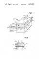
- FIG. 1is a side view in cross section of a surface emitting type IR LED fabricated in accordance with the teachings of the present invention
- FIG. 2is a top view showing the IR LED of FIG. 1 in a multiple LED array
- FIG. 3is a side view in cross section depicting an alternate surface emitting type IR LED array construction
- FIG. 4is a top view of the IR LED shown in FIG. 3 in a multiple LED array
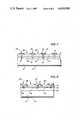
- FIG. 5is an isometric view of an edge emitting type IR LED fabricated in accordance with the teachings of the present invention.
- FIG. 6is a top view showing the IR LED of FIG. 5 in a multiple LED array
- FIG. 7is a side view in cross section of the IR LED array shown with barriers to prevent optical cross talk between adjoining LEDs.
- FIG. 8is a side view in cross section illustrating a cross talk preventing barrier formed by proton bombardment.
- Heterostructure LED array 10has a GaAs-n wafer or substrate 12, with one side 13 metallized to form a common electrical contact surface 14 for the LEDs of the array.
- a first layer 20composed of Ga 1-x Al x As-n is grown on the opposite side 15 of substrate 12 followed by a layer 22 of either GaAs-p or Ga 1-z Al z As-p and a layer 24 of Ga 1-y Al y As-p.
- the thickness of substrate 12is approximately 0.010 to 0.015 inches while the combined thickness of layers 20, 22, 24 is approximately 5 to 10 microns. Suitable ranges for x, y and z and approximate layer thicknesses for this embodiment are given in Table I.
- An electrical contact layer 28 of GaAs-p+(heavily doped p-type), which forms an electrical contact area for a metallization layer 34, is next grown over the layer 24 followed by an insulating layer 30 such as SiO 2 .
- Contact and insulating layer 28, 30are selectively etched at predetermined points to form an LED light emitting area or window 35 of predetermined dimension and configuration defining each LED 11, LEDs 11 being formed a preset spaced intervals along wafer 12 in the array configuration desired.
- LEDs 11are formed in parallel rows 36, 38 with the LEDs of each row being offset or staggered with respect to the LEDs of the other row.
- array 10is shown and described as comprising two rows of LEDs 11, array 10 may comprise one or any number of parallel rows of LEDs 11 as will be understood.
- the LEDs 11 of array 10are there formed in a single row 36'.
- contact layer 28is dispensed with and the metallization layer 34 is placed directly on third layer 24 including the light emitting windows 35 of LEDs 11.
- metallization layer 34is made extremely thin (or of a suitable transparent electrically conducting material) so that layer 34 is transparent to the light emitting windows 35 of LEDs 11. Suitable ranges for x, y and z and approximate layer thicknesses for this embodiment are given in Table II.
- array 10comprises one or more linear arrays of surface emitting LEDs.
- array 10comprises a linear array of edge emitting LEDs. Referring thereto, a first layer 50 of Ga 1-x Al x As-n is grown on substrate 12 followed by an emitting layer 52 of GaAs-p or Ga 1-z Al z As-p. In this arrangement, LEDs 11 emit from layer 52 along edge 55 of substrate 12. Layer 56 of Ga 1-y Al y As-p is grown on layer 52 followed by contact layer 28 and insulating layer 30. Suitable ranges for x, y and z and approximate layer thicknesses for this embodiment are given in Table III.
- first layer 20(FIGS. 1-4) or 50 (FIGS. 5, 6) can be as thin as approximately 0.5 to 1.0 microns.
- Insulating layer 30is selectively etched to uncover a generally rectangular area 58 of contact layer 28 above each LED 11.
- a strip-like portion 59 of metallization layer 34is removed along each side to provide electrical isolation between adjoining LEDs of the array.
- Metallization layer 34covers the areas 58 of contact layer 28 to form contact pads 60 for the LEDs 11. Leads 37 are bonded to contact pads 60.
- a light barrier 70is provided between adjoining LEDs 11.
- barrier 70is produced by etching, either chemically or through an ion etch, a channel 72 through metal contact layer 34, contact layer 28, Ga 1-y Al y As-p layer 24, GaAs-p layer 22 and either into or through the Ga 1-x As x As-n layer 20.
- the interior walls of channel 72are coated with a suitable light reflective or absorbing layer 74.
- layer 74may comprise any suitable light reflecting material such as a reflective metal with a suitable insulator layer thereunder to prevent short circuiting of the LED.
- layer 74may comprise any suitable non-conducting light absorbing material such dyed polyimide or developed, dyed photoresist.
- light barrier 70is formed by controlled proton bombardment using a mask to expose the region between adjoining LEDs 11, the latter producing a barrier region 75 of high optical absorption and high electrical resistivity. Additionally, the embodiments shown in FIGS. 7 and 8 will reduce lateral current spreading under the electrical contact 28' and in layers 28, 24, and 22 and improve the efficiency of the LEDs.
- light barrier 70is illustrated as comprising a channel-like recess having a generally rectangular shape when viewed in the cross section, other configurations such as a V-shape, may be envisioned.
- the inventionprovides high speed, high resolution heterostructure IR LEDs which consist of high quality, low strain, low dislocation density single crystals of a known and well controlled orientation, usually (100).
- Arrays 10 embodying the IR LEDs of the present inventioncan be readily cleaved in a controlled fashion as is routinely done in the fabrication of laser diodes.
- the techniques developed for the cutting and butting of silicon photodetector arraysare directly applicable thereby enabling long IR LED arrays capable of writing one or more image lines at a time to be economically formed.
- Similar heterostructure LED arraysmay also be formed using the Indium Gallium Arsenide Phosphide (InGaAsP) material system.
- the LEDsalso can operate with high efficiency and can be made for the wavelength range of approximately 1.1 to 1.7 microns.
- LED arrays of the type described hereincan also be used as photodiode arrays for image recording. Since GaAs/GaAlAs and InGaAsP are direct band gap materials, they should provide high optical absorption and efficient photodiode array systems.
Landscapes
- Led Devices (AREA)
Abstract
Description
The invention relates to LED arrays, and more particularly, to high efficiency IR or near IR LED arrays for high speed, high resolution printing.
With the advent of commercially available infra-red (I.R.) photoreceptors, the use of a Light Emitting Diode (LED) array to write images on the photoreceptor has taken on renewed interest. As will be understood, arrays of this type comprise one or more linear rows of LEDs in close juxtaposition with one another to form in effect a light bar which, through selective actuation of the individual LEDs in accordance with an image input signal, exposes the photoreceptor to create or write a latent electrostatic image thereon. The latent electrostatic image created is thereafter processed xerographically to produce a permanent visible copy of the image.
This renewed interest is primarily due to the fact that IR LEDs can be made with an efficiency more than an order of magnitude, and in some cases two orders of magnitude, greater than present day visible LEDs. Moreover, because of recent advances in materials preparation, such as Metalorganic Chemical Vapor Deposition (MOCVD) and Molecular Beam Epitaxy (M.B.E.), IR LEDs can now be made from direct gap commercially viable materials like Gallium Arsenide (GaAs) or Gallium Aluminum Arsenide (GaAlAs) in heterostructures which show reliability and uniformity much superior to previous visible LEDs. However, because these high efficiency IR LED arrays are structured differently than previous LED arrays, IR LED arrays have their own constraints and advantages.
Because of past photoreceptor spectral limitations and the consequent unavailability of IR photoreceptors, LED arrays are currently made from zinc diffused Gallium Arsenide Phosphide (Ga(As,P)) grown epitaxially on Gallium Arsenide (GaAs) or Gallium Phosphide (GaP). As will be understood, Ga(As,P) is an indirect gap semiconductor and LEDs constructed of this material are of relatively low external efficiency, usually 0.02 to 0.05%. With nitrogen doping, efficiency may be raised to 0.2 to 0.5% but there are uniformity problems associated with this.
These types of LED arrays are also lambertian radiators. The light typically must be collected by gradient index fiber lenses (with a Numerical Aperture of 0.08 to 0.3). This results in low overall optical system efficiency, usually less than 5%. Moreover, for a typical 3300 spot or pixel system, the LEDs that comprise the array must be time multiplexed by a factor of 20 or so or else 3300 drive transistors must be used. These factors combine to produce a very low level of energy at the photoreceptor, with resultant limitation of the processing speed to the approximately 2 inches/second range.
Moreover, since III-V class LED materials are easily damaged by saw cutting, etc., the small LED chips containing a plurality of LEDs cannot normally be butted together but instead must be staggered in two rows and then optically interlaced using two gradient index fiber lenses. The preferred system of cleaving and butting the LED chips cannot be done with these materials due to the large lattice mismatch, multiple networks of misfit dislocations, and the high level of strain between the Ga(As,P) and the LED substrate. Also, because of the presence of dislocation networks, LED arrays of this type tend to be non-uniform, with efficiencies typically varying by +- 20% within arrays. Further, LED arrays of this type are also subject to slow degradation, there being a statistical distribution of degradation among the individual LEDs that comprise the array, so that some LEDs degrade much faster than others. As a result, this type of LED array usually requires continuous calibration to assure overall long term uniformity of output, such calibration being typically accomplished through automatic adjustment of the drive current to each LED.
The invention seeks to obviate the foregoing problems and shortcomings of typical visible LED arrays by providing a high speed, high resolution IR LED array of high efficiency for printing images comprising: a GaAs-n wafer with one side metallized to provide a common electrical contact for the array LEDs; a first layer of Ga1-x Alx As-n on the other side of the wafer; a second layer of GaAs-p on the first layer; a third layer of Ga1-y Aly As-p on the second layer; an insulating layer of SiO2 (or other suitable insulator) on the third layer, a portion of the insulating layer being removed at selected points to expose predetermined areas of the third layer to form viewing windows for each of the LEDs; and a metallized layer on at least the exposed area of the third layer to provide electrical contacts for each of the LEDs.
The invention further relates to a method for fabricating a high speed high resolution IR LED array for printing images, comprising the steps of: metallizing one surface of a GaAs-n substrate to provide a common electrical contact for the LEDs; epitaxially growing a first layer of Ga1-x Alx As-n on the other surface of the substrate; growing a second layer of GaAs-p on the first layer; growing a third layer of Ga1-y Aly As-p on the second layer; depositing an insulating layer of SiO2 on the third layer; etching the insulating layer at selected points to expose predetermined areas of the third layer and form viewing windows defining each of the LEDs; and metallizing at least the exposed area of the third layer to provide individual electrical contacts for each of the LEDs.
FIG. 1 is a side view in cross section of a surface emitting type IR LED fabricated in accordance with the teachings of the present invention;
FIG. 2 is a top view showing the IR LED of FIG. 1 in a multiple LED array;
FIG. 3 is a side view in cross section depicting an alternate surface emitting type IR LED array construction;
FIG. 4 is a top view of the IR LED shown in FIG. 3 in a multiple LED array;
FIG. 5 is an isometric view of an edge emitting type IR LED fabricated in accordance with the teachings of the present invention;
FIG. 6 is a top view showing the IR LED of FIG. 5 in a multiple LED array;
FIG. 7 is a side view in cross section of the IR LED array shown with barriers to prevent optical cross talk between adjoining LEDs; and
FIG. 8 is a side view in cross section illustrating a cross talk preventing barrier formed by proton bombardment.
Referring now to FIGS. 1 and 2 of the drawings, a highefficiency heterostructure array 10 of IR LEDs 11 fabricated in accordance with the teachings of the present invention is there shown. In the ensuing description and drawings, Ga refers to gallium, Al to aluminum, and As to arsenic.Heterostructure LED array 10 has a GaAs-n wafer orsubstrate 12, with oneside 13 metallized to form a commonelectrical contact surface 14 for the LEDs of the array. Afirst layer 20 composed of Ga1-x Alx As-n is grown on theopposite side 15 ofsubstrate 12 followed by alayer 22 of either GaAs-p or Ga1-z Alz As-p and alayer 24 of Ga1-y Aly As-p. The thickness ofsubstrate 12 is approximately 0.010 to 0.015 inches while the combined thickness oflayers
Anelectrical contact layer 28 of GaAs-p+ (heavily doped p-type), which forms an electrical contact area for ametallization layer 34, is next grown over thelayer 24 followed by aninsulating layer 30 such as SiO2. Contact and insulatinglayer window 35 of predetermined dimension and configuration defining each LED 11, LEDs 11 being formed a preset spaced intervals alongwafer 12 in the array configuration desired. In the example shown in FIGS. 1 and 2, LEDs 11 are formed inparallel rows insulating layer 30 bordering theLED windows 35 and uncover a portion 28' ofcontact layer 28. The uncovered portions 28' ofbonding layer 28 surrounding each LED 11 is metallized at 34 to form a metal contact pad for each LED. Ametal lead 37 is bonded to each LED contact pad.
Whilearray 10 is shown and described as comprising two rows of LEDs 11,array 10 may comprise one or any number of parallel rows of LEDs 11 as will be understood.
In the embodiment shown in FIGS. 3 and 4, where like numbers refer to like parts, the LEDs 11 ofarray 10 are there formed in a single row 36'. In this embodiment,contact layer 28 is dispensed with and themetallization layer 34 is placed directly onthird layer 24 including thelight emitting windows 35 of LEDs 11. In this embodiment,metallization layer 34 is made extremely thin (or of a suitable transparent electrically conducting material) so thatlayer 34 is transparent to thelight emitting windows 35 of LEDs 11. Suitable ranges for x, y and z and approximate layer thicknesses for this embodiment are given in Table II.
In the embodiment shown in FIGS. 1-4,array 10 comprises one or more linear arrays of surface emitting LEDs. In the embodiment shown in FIGS. 5 and 6, where like numbers refer to like parts,array 10 comprises a linear array of edge emitting LEDs. Referring thereto, afirst layer 50 of Ga1-x Alx As-n is grown onsubstrate 12 followed by anemitting layer 52 of GaAs-p or Ga1-z Alz As-p. In this arrangement, LEDs 11 emit fromlayer 52 alongedge 55 ofsubstrate 12.Layer 56 of Ga1-y Aly As-p is grown onlayer 52 followed bycontact layer 28 and insulatinglayer 30. Suitable ranges for x, y and z and approximate layer thicknesses for this embodiment are given in Table III.
In all of the above structures, a layer of GaAs-n of 1 to 5 microns thick may be grown prior to the first Ga1-x Alx As layer to act as a buffer layer and improve crystal quality. If this buffer layer is used, first layer 20 (FIGS. 1-4) or 50 (FIGS. 5, 6) can be as thin as approximately 0.5 to 1.0 microns.
Referring now to the embodiments shown in FIGS. 7 and 8, where like numbers refer to like parts, to avoid crosstalk between adjoining LEDs 11 ofarray 10 due to internal material transparency which permits an "on" LED to cross couple light into an adjacent "off" LED, alight barrier 70 is provided between adjoining LEDs 11. In the arrangement shown in FIG. 7,barrier 70 is produced by etching, either chemically or through an ion etch, achannel 72 throughmetal contact layer 34,contact layer 28, Ga1-y Aly As-p layer 24, GaAs-p layer 22 and either into or through the Ga1-x Asx As-n layer 20. The interior walls ofchannel 72 are coated with a suitable light reflective or absorbinglayer 74. Where a reflective light barrier is desired,layer 74 may comprise any suitable light reflecting material such as a reflective metal with a suitable insulator layer thereunder to prevent short circuiting of the LED. Where a light absorbing layer is desired,layer 74 may comprise any suitable non-conducting light absorbing material such dyed polyimide or developed, dyed photoresist.
In the embodiment shown in FIG. 8,light barrier 70 is formed by controlled proton bombardment using a mask to expose the region between adjoining LEDs 11, the latter producing abarrier region 75 of high optical absorption and high electrical resistivity. Additionally, the embodiments shown in FIGS. 7 and 8 will reduce lateral current spreading under the electrical contact 28' and inlayers
Whilelight barrier 70 is illustrated as comprising a channel-like recess having a generally rectangular shape when viewed in the cross section, other configurations such as a V-shape, may be envisioned.
The invention provides high speed, high resolution heterostructure IR LEDs which consist of high quality, low strain, low dislocation density single crystals of a known and well controlled orientation, usually (100).Arrays 10 embodying the IR LEDs of the present invention can be readily cleaved in a controlled fashion as is routinely done in the fabrication of laser diodes. As a result, the techniques developed for the cutting and butting of silicon photodetector arrays are directly applicable thereby enabling long IR LED arrays capable of writing one or more image lines at a time to be economically formed.
Similar heterostructure LED arrays may also be formed using the Indium Gallium Arsenide Phosphide (InGaAsP) material system. The LEDs also can operate with high efficiency and can be made for the wavelength range of approximately 1.1 to 1.7 microns.
As has been described in U.S. Pat. No. 4,424,524 issued on Jan. 3, 1984 to Joseph J. Daniele et al, LED arrays of the type described herein can also be used as photodiode arrays for image recording. Since GaAs/GaAlAs and InGaAsP are direct band gap materials, they should provide high optical absorption and efficient photodiode array systems.
TABLE I ______________________________________ Approximate Compositions And Thicknesses Of Various Layers Shown In FIGS. 1 and 2: Approx. Composition Layer (atomic fraction) Approx. Thickness (microns) ______________________________________ 20 x = 0.2 to 0.5 2 to 10 22 z = 0.0 (GaAs) 0.3 to 1.0 24 y = 0.2 to 0.5 1 to 2 28 0.0 0.2 to 1.0 20 x = z + (0.2 to 0.5) 2 to 10 22 z = 0.0 to 0.30 0.3 to 1.0 24 y = z + (0.2 to 0.5) 1 to 2 28 0.0 0.2 to 1.0 ______________________________________
TABLE II ______________________________________ Approximate Compositions And Thicknesses Of Various Layers Shown In FIGS. 3 and 4: Approx. Composition Layer (atomic fraction) Approx. Thickness (microns) ______________________________________ 20 x = 0.3 to 0.6 2 to 10 22 z = 0.0 (GaAs) 0.3 to 1.0 24 y = 0.1 to 0.35 1 to 2 20 x = z + (0.3 to 0.6) 2 to 10 22 z = 0.0 to 0.2 0.3 to 1.0 24 y = z + (0.1 to 0.15) 1 to 2 ______________________________________
TABLE III ______________________________________ Approximate Compositions And Thicknesses Of Various Layers Shown In FIGS. 5 and 6: Approx. Composition Layer (atomic fraction) Approx. Thickness (microns) ______________________________________ 50 x = z + (0.3 to 0.5) 2 to 10 52 z = 0.0 to 0.30 0.3 to 1 56 y = z + (0.3 to 0.5) 0.5 to 1.0 28 0.0 0.2 to 0.5 ______________________________________
While the invention has been described with reference to the structure disclosed, it is not confined to the details set forth, but is intended to cover such modifications or changes as may come within the scope of the following claims.
Claims (9)
1. A method of fabricating a high speed, high resolution IR LED array for printing images, comprising the steps of:
(a) metallizing one surface of a GaAs-n substrate to provide a common electrical contact for said LEDs;
(b) growing a first layer of GaAlAs-n on the other surface of said substrate;
(c) growing a second layer of GaAs-p or GaAlAs on said first layer;
(d) growing a third layer of GaAlAs-p on said second layer;
(e) growing an electrical contact layer of GaAs-p+ on said third layer;
(f) depositing an insulating layer on said electrical contact layer;
(g) etching both said insulating and said contact layers at selected points to expose predetermined areas of said third layer and form viewing windows defining each of said LEDs;
(h) etching said portion of said insulating layer in the area bounding each of said viewing windows to expose a portion of said contact layer; and
(i) metallizing said exposed portions of said contact layer to provide said individual electrical contacts for each of said LEDs.
2. The method according to claim 1 including the step of:
metallizing both said third layer areas comprising said viewing windows together with the portion of said contact layer bounding said viewing windows with a transparent electrically conducting covering to provide said electrical contacts for each of said LEDs.
3. A method of fabricating a high speed, high resolution IR LED array for printing images, comprising the steps of:
(a) metallizing one surface of a GaAs-n substrate to provide a common electrical contact for said LEDs;
(b) growing a first layer of GaAlAs-n on the other surface of said substrate;
(c) growing a second layer of GaAs-p or GaAlAs on said first layer;
(d) growing a third layer of GaAlAs-p on said second layer;
(e) depositing an insulating layer on said third layer;
(f) etching said insulating layer at selected points to expose predetermined areas of said third layer and form viewing windows defining each of said LEDs;
(g) metallizing the areas of said third layer comprising each of said viewing windows to provide individual electrical contacts for each of said LEDs; and
(h) forming a light barrier between adjoining ones of said LEDs to prevent optical crosstalk between said adjoining LEDs.
4. The method according to claim 3 including the step of:
forming said light barrier by etching a recess through said insulating, contacting, third, and second layers and into or through said first layer.
5. The method according to claim 4 including the step of:
coating the inside walls of said light barrier with a light reflecting material.
6. The method according to claim 4 including the step of:
coating the inside walls of said light barrier with a light absorbing material.
7. The method according to claim 3 including the step of:
forming said light barrier by proton bombardment.
8. The method according to claim 4 including the step of:
etching a rectangular recess for said light barrier.
9. The method according to claim 4 including the step of:
etching a V-shaped recess for said light barrier.
Priority Applications (5)
| Application Number | Priority Date | Filing Date | Title |
|---|---|---|---|
| US06/667,706US4639999A (en) | 1984-11-02 | 1984-11-02 | High resolution, high efficiency I.R. LED printing array fabrication method |
| JP23718885AJPH0736449B2 (en) | 1984-11-02 | 1985-10-23 | Manufacturing method of light emitting diode printed array |
| DE8585307912TDE3586196T2 (en) | 1984-11-02 | 1985-10-31 | LIGHT-EMITTING DIODE ARRANGEMENT. |
| EP85307912AEP0180479B1 (en) | 1984-11-02 | 1985-10-31 | Light-emitting diode array |
| US06/895,983US4707716A (en) | 1984-11-02 | 1986-08-14 | High resolution, high efficiency I.R. LED printing array and fabrication method |
Applications Claiming Priority (1)
| Application Number | Priority Date | Filing Date | Title |
|---|---|---|---|
| US06/667,706US4639999A (en) | 1984-11-02 | 1984-11-02 | High resolution, high efficiency I.R. LED printing array fabrication method |
Related Child Applications (1)
| Application Number | Title | Priority Date | Filing Date |
|---|---|---|---|
| US06/895,983DivisionUS4707716A (en) | 1984-11-02 | 1986-08-14 | High resolution, high efficiency I.R. LED printing array and fabrication method |
Publications (1)
| Publication Number | Publication Date |
|---|---|
| US4639999Atrue US4639999A (en) | 1987-02-03 |
Family
ID=24679301
Family Applications (1)
| Application Number | Title | Priority Date | Filing Date |
|---|---|---|---|
| US06/667,706Expired - Fee RelatedUS4639999A (en) | 1984-11-02 | 1984-11-02 | High resolution, high efficiency I.R. LED printing array fabrication method |
Country Status (1)
| Country | Link |
|---|---|
| US (1) | US4639999A (en) |
Cited By (85)
| Publication number | Priority date | Publication date | Assignee | Title |
|---|---|---|---|---|
| US5204284A (en)* | 1989-01-19 | 1993-04-20 | Hewlett-Packard Company | Method of making a high band-gap opto-electronic device |
| US5453386A (en)* | 1994-05-09 | 1995-09-26 | Motorola, Inc. | Method of fabrication of implanted LED array |
| US5501990A (en)* | 1994-05-09 | 1996-03-26 | Motorola, Inc. | High density LED arrays with semiconductor interconnects |
| US6518080B2 (en)* | 2001-06-19 | 2003-02-11 | Sensors Unlimited, Inc. | Method of fabricating low dark current photodiode arrays |
| US6743990B1 (en)* | 2002-12-12 | 2004-06-01 | Agilent Technologies, Inc. | Volume adjustment apparatus and method for use |
| US20040112728A1 (en)* | 2002-12-12 | 2004-06-17 | Wong Marvin Glenn | Ceramic channel plate for a switch |
| US20060058592A1 (en)* | 2004-08-24 | 2006-03-16 | The General Hospital Corporation | Process, system and software arrangement for measuring a mechanical strain and elastic properties of a sample |
| US20060058622A1 (en)* | 2004-08-24 | 2006-03-16 | The General Hospital Corporation | Method and apparatus for imaging of vessel segments |
| US20060114473A1 (en)* | 2004-11-29 | 2006-06-01 | The General Hospital Corporation | Arrangements, devices, endoscopes, catheters and methods for performing optical imaging by simultaneously illuminating and detecting multiple points on a sample |
| US20060270929A1 (en)* | 2005-05-31 | 2006-11-30 | The General Hospital Corporation | System, method and arrangement which can use spectral encoding heterodyne interferometry techniques for imaging |
| US20070012886A1 (en)* | 2005-04-28 | 2007-01-18 | The General Hospital Corporation | Systems. processes and software arrangements for evaluating information associated with an anatomical structure by an optical coherence ranging technique |
| US20070049833A1 (en)* | 2005-08-16 | 2007-03-01 | The General Hospital Corporation | Arrangements and methods for imaging in vessels |
| US20070081236A1 (en)* | 2005-09-29 | 2007-04-12 | The General Hospital Corporation | Method and apparatus for optical imaging via spectral encoding |
| US20070087445A1 (en)* | 2005-10-14 | 2007-04-19 | The General Hospital Corporation | Arrangements and methods for facilitating photoluminescence imaging |
| US20070179487A1 (en)* | 2006-02-01 | 2007-08-02 | The General Hospital Corporation | Apparatus for applying a plurality of electro-magnetic radiations to a sample |
| US20070188855A1 (en)* | 2006-01-19 | 2007-08-16 | The General Hospital Corporation | Apparatus for obtaining information for a structure using spectrally-encoded endoscopy teachniques and methods for producing one or more optical arrangements |
| US20070201033A1 (en)* | 2006-02-24 | 2007-08-30 | The General Hospital Corporation | Methods and systems for performing angle-resolved fourier-domain optical coherence tomography |
| US20070238955A1 (en)* | 2006-01-18 | 2007-10-11 | The General Hospital Corporation | Systems and methods for generating data using one or more endoscopic microscopy techniques |
| US20070276269A1 (en)* | 2006-05-10 | 2007-11-29 | The General Hospital Corporation | Process, arrangements and systems for providing frequency domain imaging of a sample |
| US20080002211A1 (en)* | 2006-01-20 | 2008-01-03 | The General Hospital Corporation | System, arrangement and process for providing speckle reductions using a wave front modulation for optical coherence tomography |
| US20080013960A1 (en)* | 2000-11-10 | 2008-01-17 | The General Hospital Corporation | Apparatus and method for providing information for at least one structure |
| US20080021275A1 (en)* | 2006-01-19 | 2008-01-24 | The General Hospital Corporation | Methods and systems for optical imaging or epithelial luminal organs by beam scanning thereof |
| US20080094613A1 (en)* | 2003-01-24 | 2008-04-24 | The General Hospital Corporation | Apparatus and method for ranging and noise reduction of low coherence interferometry lci and optical coherence tomography oct signals by parallel detection of spectral bands |
| US20080097225A1 (en)* | 2006-10-19 | 2008-04-24 | The General Hospital Corporation | Apparatus and method for obtaining and providing imaging information associated with at least one portion of a sample, and effecting such portion(s) |
| US20080232410A1 (en)* | 2007-03-23 | 2008-09-25 | The General Hospital Corporation | Methods, arrangements and apparatus for utilizing a wavelength-swept laser using angular scanning and dispersion procedures |
| US20080234567A1 (en)* | 2007-03-19 | 2008-09-25 | The General Hospital Corporation | Apparatus and method for providing a noninvasive diagnosis of internal bleeding |
| US20080262314A1 (en)* | 2007-04-17 | 2008-10-23 | The General Hospital Corporation | Apparatus and methods for measuring vibrations using spectrally-encoded endoscopy |
| US20080262359A1 (en)* | 2007-03-30 | 2008-10-23 | The General Hospital Corporation | System and method providing intracoronary laser speckle imaging for the detection of vulnerable plaque |
| US20080297806A1 (en)* | 2007-01-19 | 2008-12-04 | The General Hospital Corporation | Apparatus and method for controlling ranging depth in optical frequency domain imaging |
| US20090036770A1 (en)* | 2001-05-01 | 2009-02-05 | The General Hospital Corporation | Method and apparatus for determination of atherosclerotic plaque type by measurement of tissue optical properties |
| US20090073439A1 (en)* | 2007-09-15 | 2009-03-19 | The General Hospital Corporation | Apparatus, computer-accessible medium and method for measuring chemical and/or molecular compositions of coronary atherosclerotic plaques in anatomical structures |
| US20090131801A1 (en)* | 2007-10-12 | 2009-05-21 | The General Hospital Corporation | Systems and processes for optical imaging of luminal anatomic structures |
| US20090196477A1 (en)* | 2004-05-29 | 2009-08-06 | The General Hospital Corporation | Process, System And Software Arrangement For A Chromatic Dispersion Compensation Using Reflective Layers In Optical Coherence Tomography (OCT) Imaging |
| US20090257461A1 (en)* | 2003-06-06 | 2009-10-15 | The General Hospital Corporation | Process and apparatus for a wavelength tuning source |
| US20100094576A1 (en)* | 2002-01-24 | 2010-04-15 | The General Hospital Corporation | Apparatus and method for ranging and noise reduction of low coherence interferometry lci and optical coherence tomography oct signals by parallel detection of spectral bands |
| US20100110414A1 (en)* | 2008-05-07 | 2010-05-06 | The General Hospital Corporation | System, method and computer-accessible medium for tracking vessel motion during three-dimensional coronary artery microscopy |
| US20100150422A1 (en)* | 2008-12-10 | 2010-06-17 | The General Hospital Corporation | Systems and Methods for Extending Imaging Depth Range of Optical Coherence Tomography Through Optical Sub-Sampling |
| US20100165335A1 (en)* | 2006-08-01 | 2010-07-01 | The General Hospital Corporation | Systems and methods for receiving and/or analyzing information associated with electro-magnetic radiation |
| US20100210937A1 (en)* | 2009-01-20 | 2010-08-19 | The General Hospital Corporation | Endoscopic biopsy apparatus, system and method |
| US20100254415A1 (en)* | 2009-02-04 | 2010-10-07 | The General Hospital Corporation | Apparatus and method for utilization of a high-speed optical wavelength tuning source |
| US7898656B2 (en) | 2008-04-30 | 2011-03-01 | The General Hospital Corporation | Apparatus and method for cross axis parallel spectroscopy |
| US7925133B2 (en) | 2004-07-02 | 2011-04-12 | The General Hospital Corporation | Imaging system and related techniques |
| US20110092823A1 (en)* | 2003-01-24 | 2011-04-21 | The General Hospital Corporation | System and Method for Identifying Tissue Using Low-Coherence Interferometry |
| US20110137178A1 (en)* | 2009-10-06 | 2011-06-09 | The General Hospital Corporation | Devices and methods for imaging particular cells including eosinophils |
| US20110137140A1 (en)* | 2009-07-14 | 2011-06-09 | The General Hospital Corporation | Apparatus, Systems and Methods for Measuring Flow and Pressure within a Vessel |
| US20110222563A1 (en)* | 2007-01-19 | 2011-09-15 | The General Hospital Corporation | Wavelength tuning source based on a rotatable reflector |
| US20110224541A1 (en)* | 2009-12-08 | 2011-09-15 | The General Hospital Corporation | Methods and arrangements for analysis, diagnosis, and treatment monitoring of vocal folds by optical coherence tomography |
| US20110226940A1 (en)* | 2008-06-20 | 2011-09-22 | The General Hospital Corporation | Fused fiber optic coupler arrangement and method for use thereof |
| US8097864B2 (en) | 2009-01-26 | 2012-01-17 | The General Hospital Corporation | System, method and computer-accessible medium for providing wide-field superresolution microscopy |
| US8174702B2 (en) | 2003-01-24 | 2012-05-08 | The General Hospital Corporation | Speckle reduction in optical coherence tomography by path length encoded angular compounding |
| USRE44042E1 (en) | 2004-09-10 | 2013-03-05 | The General Hospital Corporation | System and method for optical coherence imaging |
| US8705046B2 (en) | 2003-10-27 | 2014-04-22 | The General Hospital Corporation | Method and apparatus for performing optical imaging using frequency-domain interferometry |
| US8804126B2 (en) | 2010-03-05 | 2014-08-12 | The General Hospital Corporation | Systems, methods and computer-accessible medium which provide microscopic images of at least one anatomical structure at a particular resolution |
| USRE45512E1 (en) | 2004-09-29 | 2015-05-12 | The General Hospital Corporation | System and method for optical coherence imaging |
| US9060689B2 (en) | 2005-06-01 | 2015-06-23 | The General Hospital Corporation | Apparatus, method and system for performing phase-resolved optical frequency domain imaging |
| US9069130B2 (en) | 2010-05-03 | 2015-06-30 | The General Hospital Corporation | Apparatus, method and system for generating optical radiation from biological gain media |
| US9226660B2 (en) | 2004-08-06 | 2016-01-05 | The General Hospital Corporation | Process, system and software arrangement for determining at least one location in a sample using an optical coherence tomography |
| US9282931B2 (en) | 2000-10-30 | 2016-03-15 | The General Hospital Corporation | Methods for tissue analysis |
| US9330092B2 (en) | 2011-07-19 | 2016-05-03 | The General Hospital Corporation | Systems, methods, apparatus and computer-accessible-medium for providing polarization-mode dispersion compensation in optical coherence tomography |
| US9341783B2 (en) | 2011-10-18 | 2016-05-17 | The General Hospital Corporation | Apparatus and methods for producing and/or providing recirculating optical delay(s) |
| US9415550B2 (en) | 2012-08-22 | 2016-08-16 | The General Hospital Corporation | System, method, and computer-accessible medium for fabrication miniature endoscope using soft lithography |
| US9441948B2 (en) | 2005-08-09 | 2016-09-13 | The General Hospital Corporation | Apparatus, methods and storage medium for performing polarization-based quadrature demodulation in optical coherence tomography |
| US9510758B2 (en) | 2010-10-27 | 2016-12-06 | The General Hospital Corporation | Apparatus, systems and methods for measuring blood pressure within at least one vessel |
| US9557154B2 (en) | 2010-05-25 | 2017-01-31 | The General Hospital Corporation | Systems, devices, methods, apparatus and computer-accessible media for providing optical imaging of structures and compositions |
| US9629528B2 (en) | 2012-03-30 | 2017-04-25 | The General Hospital Corporation | Imaging system, method and distal attachment for multidirectional field of view endoscopy |
| US9733460B2 (en) | 2014-01-08 | 2017-08-15 | The General Hospital Corporation | Method and apparatus for microscopic imaging |
| US9777053B2 (en) | 2006-02-08 | 2017-10-03 | The General Hospital Corporation | Methods, arrangements and systems for obtaining information associated with an anatomical sample using optical microscopy |
| US9784681B2 (en) | 2013-05-13 | 2017-10-10 | The General Hospital Corporation | System and method for efficient detection of the phase and amplitude of a periodic modulation associated with self-interfering fluorescence |
| US9795301B2 (en) | 2010-05-25 | 2017-10-24 | The General Hospital Corporation | Apparatus, systems, methods and computer-accessible medium for spectral analysis of optical coherence tomography images |
| US9968261B2 (en) | 2013-01-28 | 2018-05-15 | The General Hospital Corporation | Apparatus and method for providing diffuse spectroscopy co-registered with optical frequency domain imaging |
| US10058250B2 (en) | 2013-07-26 | 2018-08-28 | The General Hospital Corporation | System, apparatus and method for utilizing optical dispersion for fourier-domain optical coherence tomography |
| US10117576B2 (en) | 2013-07-19 | 2018-11-06 | The General Hospital Corporation | System, method and computer accessible medium for determining eye motion by imaging retina and providing feedback for acquisition of signals from the retina |
| US10228556B2 (en) | 2014-04-04 | 2019-03-12 | The General Hospital Corporation | Apparatus and method for controlling propagation and/or transmission of electromagnetic radiation in flexible waveguide(s) |
| US10241028B2 (en) | 2011-08-25 | 2019-03-26 | The General Hospital Corporation | Methods, systems, arrangements and computer-accessible medium for providing micro-optical coherence tomography procedures |
| US10285568B2 (en) | 2010-06-03 | 2019-05-14 | The General Hospital Corporation | Apparatus and method for devices for imaging structures in or at one or more luminal organs |
| US10426548B2 (en) | 2006-02-01 | 2019-10-01 | The General Hosppital Corporation | Methods and systems for providing electromagnetic radiation to at least one portion of a sample using conformal laser therapy procedures |
| US10478072B2 (en) | 2013-03-15 | 2019-11-19 | The General Hospital Corporation | Methods and system for characterizing an object |
| US10736494B2 (en) | 2014-01-31 | 2020-08-11 | The General Hospital Corporation | System and method for facilitating manual and/or automatic volumetric imaging with real-time tension or force feedback using a tethered imaging device |
| US10835110B2 (en) | 2008-07-14 | 2020-11-17 | The General Hospital Corporation | Apparatus and method for facilitating at least partial overlap of dispersed ration on at least one sample |
| US10893806B2 (en) | 2013-01-29 | 2021-01-19 | The General Hospital Corporation | Apparatus, systems and methods for providing information regarding the aortic valve |
| DE102020001844B3 (en)* | 2020-03-20 | 2021-01-28 | Azur Space Solar Power Gmbh | Stacked III-V photonic semiconductor device |
| US10912462B2 (en) | 2014-07-25 | 2021-02-09 | The General Hospital Corporation | Apparatus, devices and methods for in vivo imaging and diagnosis |
| US11179028B2 (en) | 2013-02-01 | 2021-11-23 | The General Hospital Corporation | Objective lens arrangement for confocal endomicroscopy |
| US11452433B2 (en) | 2013-07-19 | 2022-09-27 | The General Hospital Corporation | Imaging apparatus and method which utilizes multidirectional field of view endoscopy |
| US11490797B2 (en) | 2012-05-21 | 2022-11-08 | The General Hospital Corporation | Apparatus, device and method for capsule microscopy |
Citations (17)
| Publication number | Priority date | Publication date | Assignee | Title |
|---|---|---|---|---|
| US3758875A (en)* | 1970-05-01 | 1973-09-11 | Bell Telephone Labor Inc | Double heterostructure junction lasers |
| US3899826A (en)* | 1971-12-20 | 1975-08-19 | Motorola Inc | Scannable light emitting diode array and method |
| US3912556A (en)* | 1971-10-27 | 1975-10-14 | Motorola Inc | Method of fabricating a scannable light emitting diode array |
| US4196508A (en)* | 1977-09-01 | 1980-04-08 | Honeywell Inc. | Durable insulating protective layer for hybrid CCD/mosaic IR detector array |
| US4213805A (en)* | 1973-05-28 | 1980-07-22 | Hitachi, Ltd. | Liquid phase epitaxy method of forming a filimentary laser device |
| US4331938A (en)* | 1980-08-25 | 1982-05-25 | Rca Corporation | Injection laser diode array having high conductivity regions in the substrate |
| US4339689A (en)* | 1979-01-29 | 1982-07-13 | Matsushita Electric Industrial Co., Ltd. | Light emitting diode and method of making the same |
| US4408331A (en)* | 1981-03-25 | 1983-10-04 | Bell Telephone Laboratories, Incorporated | V-Groove semiconductor light emitting devices |
| US4416011A (en)* | 1981-07-06 | 1983-11-15 | Rca Corporation | Semiconductor light emitting device |
| US4418472A (en)* | 1981-11-23 | 1983-12-06 | Xerox Corporation | Method of delineating thin film magnetic head arrays |
| US4429395A (en)* | 1981-06-01 | 1984-01-31 | Rca Corporation | Semiconductor laser |
| US4438446A (en)* | 1981-05-29 | 1984-03-20 | Bell Telephone Laboratories, Incorporated | Double barrier double heterostructure laser |
| US4445125A (en)* | 1982-04-19 | 1984-04-24 | Xerox Corporation | Diode laser array system for printing and copying applications |
| US4504952A (en)* | 1982-06-01 | 1985-03-12 | At&T Bell Laboratories | Stripe-guide TJS laser |
| US4546480A (en)* | 1983-08-19 | 1985-10-08 | Xerox Corporation | Injection lasers with quantum size effect transparent waveguiding |
| US4547956A (en)* | 1982-04-08 | 1985-10-22 | Noureddine Bouadma | Process for producing a semiconductor laser with several independent wavelengths and laser obtained by this process |
| US4587717A (en)* | 1985-05-02 | 1986-05-13 | Xerox Corporation | LED printing array fabrication method |
- 1984
- 1984-11-02USUS06/667,706patent/US4639999A/ennot_activeExpired - Fee Related
Patent Citations (17)
| Publication number | Priority date | Publication date | Assignee | Title |
|---|---|---|---|---|
| US3758875A (en)* | 1970-05-01 | 1973-09-11 | Bell Telephone Labor Inc | Double heterostructure junction lasers |
| US3912556A (en)* | 1971-10-27 | 1975-10-14 | Motorola Inc | Method of fabricating a scannable light emitting diode array |
| US3899826A (en)* | 1971-12-20 | 1975-08-19 | Motorola Inc | Scannable light emitting diode array and method |
| US4213805A (en)* | 1973-05-28 | 1980-07-22 | Hitachi, Ltd. | Liquid phase epitaxy method of forming a filimentary laser device |
| US4196508A (en)* | 1977-09-01 | 1980-04-08 | Honeywell Inc. | Durable insulating protective layer for hybrid CCD/mosaic IR detector array |
| US4339689A (en)* | 1979-01-29 | 1982-07-13 | Matsushita Electric Industrial Co., Ltd. | Light emitting diode and method of making the same |
| US4331938A (en)* | 1980-08-25 | 1982-05-25 | Rca Corporation | Injection laser diode array having high conductivity regions in the substrate |
| US4408331A (en)* | 1981-03-25 | 1983-10-04 | Bell Telephone Laboratories, Incorporated | V-Groove semiconductor light emitting devices |
| US4438446A (en)* | 1981-05-29 | 1984-03-20 | Bell Telephone Laboratories, Incorporated | Double barrier double heterostructure laser |
| US4429395A (en)* | 1981-06-01 | 1984-01-31 | Rca Corporation | Semiconductor laser |
| US4416011A (en)* | 1981-07-06 | 1983-11-15 | Rca Corporation | Semiconductor light emitting device |
| US4418472A (en)* | 1981-11-23 | 1983-12-06 | Xerox Corporation | Method of delineating thin film magnetic head arrays |
| US4547956A (en)* | 1982-04-08 | 1985-10-22 | Noureddine Bouadma | Process for producing a semiconductor laser with several independent wavelengths and laser obtained by this process |
| US4445125A (en)* | 1982-04-19 | 1984-04-24 | Xerox Corporation | Diode laser array system for printing and copying applications |
| US4504952A (en)* | 1982-06-01 | 1985-03-12 | At&T Bell Laboratories | Stripe-guide TJS laser |
| US4546480A (en)* | 1983-08-19 | 1985-10-08 | Xerox Corporation | Injection lasers with quantum size effect transparent waveguiding |
| US4587717A (en)* | 1985-05-02 | 1986-05-13 | Xerox Corporation | LED printing array fabrication method |
Non-Patent Citations (12)
| Title |
|---|
| Berkenblit et al, "Fabricating Light Emitting Diodes", IBM Technical Disclosure Bulletin, vol. 13, No. 6, Nov. 1970. |
| Berkenblit et al, Fabricating Light Emitting Diodes , IBM Technical Disclosure Bulletin, vol. 13, No. 6, Nov. 1970.* |
| Marihace et al, "Electroluminescent Anodes & Arrays", IBM Technical Disclosure Bulletin, vol. 8, No. 11, Apr. 1966. |
| Marihace et al, Electroluminescent Anodes & Arrays , IBM Technical Disclosure Bulletin, vol. 8, No. 11, Apr. 1966.* |
| Pickar et al, "Fabrication for Light-Emitting Diode Array", IBM Tech. Dis. Bull., vol. 16, No. 10, Mar. 1974. |
| Pickar et al, Fabrication for Light Emitting Diode Array , IBM Tech. Dis. Bull., vol. 16, No. 10, Mar. 1974.* |
| T. Sugahara et al, "High Radiance AlGaAs DH LED Array by MBE", Fujitsu Sci. Tech. J., 19, 3, pp. 315-322, Sep. 1983. |
| T. Sugahara et al, "Monolithic 1×4 Array of Uniform Radiance AlGaAs-GaAs LED's Grown by Molecular Beam Epitaxy", Jpn. J. Appl. Phys. 21, 6, pp. L349-350, 1982. |
| T. Sugahara et al, High Radiance AlGaAs DH LED Array by MBE , Fujitsu Sci. Tech. J., 19, 3, pp. 315 322, Sep. 1983.* |
| T. Sugahara et al, Monolithic 1 4 Array of Uniform Radiance AlGaAs GaAs LED s Grown by Molecular Beam Epitaxy , Jpn. J. Appl. Phys. 21, 6, pp. L349 350, 1982.* |
| Yeh et al, "Light-Emitting Diode Array", IBM Technical Disclosure Bulletin, vol. 9, No. 3, Aug. 1966. |
| Yeh et al, Light Emitting Diode Array , IBM Technical Disclosure Bulletin, vol. 9, No. 3, Aug. 1966.* |
Cited By (158)
| Publication number | Priority date | Publication date | Assignee | Title |
|---|---|---|---|---|
| US5204284A (en)* | 1989-01-19 | 1993-04-20 | Hewlett-Packard Company | Method of making a high band-gap opto-electronic device |
| US5453386A (en)* | 1994-05-09 | 1995-09-26 | Motorola, Inc. | Method of fabrication of implanted LED array |
| US5501990A (en)* | 1994-05-09 | 1996-03-26 | Motorola, Inc. | High density LED arrays with semiconductor interconnects |
| US9282931B2 (en) | 2000-10-30 | 2016-03-15 | The General Hospital Corporation | Methods for tissue analysis |
| US20080013960A1 (en)* | 2000-11-10 | 2008-01-17 | The General Hospital Corporation | Apparatus and method for providing information for at least one structure |
| US9295391B1 (en) | 2000-11-10 | 2016-03-29 | The General Hospital Corporation | Spectrally encoded miniature endoscopic imaging probe |
| US8050747B2 (en) | 2001-05-01 | 2011-11-01 | The General Hospital Corporation | Method and apparatus for determination of atherosclerotic plaque type by measurement of tissue optical properties |
| US20090043192A1 (en)* | 2001-05-01 | 2009-02-12 | The General Hospital Corporation | Method and apparatus for determination of atherosclerotic plaque type by measurement of tissue optical properties |
| US20090036770A1 (en)* | 2001-05-01 | 2009-02-05 | The General Hospital Corporation | Method and apparatus for determination of atherosclerotic plaque type by measurement of tissue optical properties |
| US8150496B2 (en) | 2001-05-01 | 2012-04-03 | The General Hospital Corporation | Method and apparatus for determination of atherosclerotic plaque type by measurement of tissue optical properties |
| US6518080B2 (en)* | 2001-06-19 | 2003-02-11 | Sensors Unlimited, Inc. | Method of fabricating low dark current photodiode arrays |
| US20100094576A1 (en)* | 2002-01-24 | 2010-04-15 | The General Hospital Corporation | Apparatus and method for ranging and noise reduction of low coherence interferometry lci and optical coherence tomography oct signals by parallel detection of spectral bands |
| US7903257B2 (en) | 2002-01-24 | 2011-03-08 | The General Hospital Corporation | Apparatus and method for ranging and noise reduction of low coherence interferometry (LCI) and optical coherence tomography (OCT) signals by parallel detection of spectral bands |
| US7872757B2 (en) | 2002-01-24 | 2011-01-18 | The General Hospital Corporation | Apparatus and method for ranging and noise reduction of low coherence interferometry LCI and optical coherence tomography OCT signals by parallel detection of spectral bands |
| US20050051412A1 (en)* | 2002-12-12 | 2005-03-10 | Wong Marvin Glenn | Ceramic channel plate for a fluid-based switch, and method for making same |
| US6855898B2 (en)* | 2002-12-12 | 2005-02-15 | Agilent Technologies, Inc. | Ceramic channel plate for a switch |
| US6743990B1 (en)* | 2002-12-12 | 2004-06-01 | Agilent Technologies, Inc. | Volume adjustment apparatus and method for use |
| US20040112724A1 (en)* | 2002-12-12 | 2004-06-17 | Wong Marvin Glenn | Volume adjustment apparatus and method for use |
| US20040112728A1 (en)* | 2002-12-12 | 2004-06-17 | Wong Marvin Glenn | Ceramic channel plate for a switch |
| US6924444B2 (en) | 2002-12-12 | 2005-08-02 | Agilent Technologies, Inc. | Ceramic channel plate for a fluid-based switch, and method for making same |
| US20110092823A1 (en)* | 2003-01-24 | 2011-04-21 | The General Hospital Corporation | System and Method for Identifying Tissue Using Low-Coherence Interferometry |
| US8054468B2 (en) | 2003-01-24 | 2011-11-08 | The General Hospital Corporation | Apparatus and method for ranging and noise reduction of low coherence interferometry LCI and optical coherence tomography OCT signals by parallel detection of spectral bands |
| US9226665B2 (en) | 2003-01-24 | 2016-01-05 | The General Hospital Corporation | Speckle reduction in optical coherence tomography by path length encoded angular compounding |
| US8559012B2 (en) | 2003-01-24 | 2013-10-15 | The General Hospital Corporation | Speckle reduction in optical coherence tomography by path length encoded angular compounding |
| US20080094613A1 (en)* | 2003-01-24 | 2008-04-24 | The General Hospital Corporation | Apparatus and method for ranging and noise reduction of low coherence interferometry lci and optical coherence tomography oct signals by parallel detection of spectral bands |
| US8174702B2 (en) | 2003-01-24 | 2012-05-08 | The General Hospital Corporation | Speckle reduction in optical coherence tomography by path length encoded angular compounding |
| US8416818B2 (en) | 2003-06-06 | 2013-04-09 | The General Hospital Corporation | Process and apparatus for a wavelength tuning source |
| US7995627B2 (en) | 2003-06-06 | 2011-08-09 | The General Hospital Corporation | Process and apparatus for a wavelength tuning source |
| US20090257461A1 (en)* | 2003-06-06 | 2009-10-15 | The General Hospital Corporation | Process and apparatus for a wavelength tuning source |
| USRE47675E1 (en) | 2003-06-06 | 2019-10-29 | The General Hospital Corporation | Process and apparatus for a wavelength tuning source |
| US7864822B2 (en) | 2003-06-06 | 2011-01-04 | The General Hospital Corporation | Process and apparatus for a wavelength tuning source |
| US8705046B2 (en) | 2003-10-27 | 2014-04-22 | The General Hospital Corporation | Method and apparatus for performing optical imaging using frequency-domain interferometry |
| US9377290B2 (en) | 2003-10-27 | 2016-06-28 | The General Hospital Corporation | Method and apparatus for performing optical imaging using frequency-domain interferometry |
| US8018598B2 (en) | 2004-05-29 | 2011-09-13 | The General Hospital Corporation | Process, system and software arrangement for a chromatic dispersion compensation using reflective layers in optical coherence tomography (OCT) imaging |
| US20090196477A1 (en)* | 2004-05-29 | 2009-08-06 | The General Hospital Corporation | Process, System And Software Arrangement For A Chromatic Dispersion Compensation Using Reflective Layers In Optical Coherence Tomography (OCT) Imaging |
| US7925133B2 (en) | 2004-07-02 | 2011-04-12 | The General Hospital Corporation | Imaging system and related techniques |
| US8369669B2 (en) | 2004-07-02 | 2013-02-05 | The General Hospital Corporation | Imaging system and related techniques |
| US8676013B2 (en) | 2004-07-02 | 2014-03-18 | The General Hospital Corporation | Imaging system using and related techniques |
| US9664615B2 (en) | 2004-07-02 | 2017-05-30 | The General Hospital Corporation | Imaging system and related techniques |
| US9226660B2 (en) | 2004-08-06 | 2016-01-05 | The General Hospital Corporation | Process, system and software arrangement for determining at least one location in a sample using an optical coherence tomography |
| US20060058622A1 (en)* | 2004-08-24 | 2006-03-16 | The General Hospital Corporation | Method and apparatus for imaging of vessel segments |
| US8208995B2 (en) | 2004-08-24 | 2012-06-26 | The General Hospital Corporation | Method and apparatus for imaging of vessel segments |
| US8965487B2 (en) | 2004-08-24 | 2015-02-24 | The General Hospital Corporation | Process, system and software arrangement for measuring a mechanical strain and elastic properties of a sample |
| US20110178398A1 (en)* | 2004-08-24 | 2011-07-21 | The General Hospital Corporation | Method and apparatus for imaging of vessel segments |
| US9254102B2 (en) | 2004-08-24 | 2016-02-09 | The General Hospital Corporation | Method and apparatus for imaging of vessel segments |
| US9763623B2 (en) | 2004-08-24 | 2017-09-19 | The General Hospital Corporation | Method and apparatus for imaging of vessel segments |
| US20060058592A1 (en)* | 2004-08-24 | 2006-03-16 | The General Hospital Corporation | Process, system and software arrangement for measuring a mechanical strain and elastic properties of a sample |
| USRE44042E1 (en) | 2004-09-10 | 2013-03-05 | The General Hospital Corporation | System and method for optical coherence imaging |
| USRE45512E1 (en) | 2004-09-29 | 2015-05-12 | The General Hospital Corporation | System and method for optical coherence imaging |
| US8922781B2 (en) | 2004-11-29 | 2014-12-30 | The General Hospital Corporation | Arrangements, devices, endoscopes, catheters and methods for performing optical imaging by simultaneously illuminating and detecting multiple points on a sample |
| US20060114473A1 (en)* | 2004-11-29 | 2006-06-01 | The General Hospital Corporation | Arrangements, devices, endoscopes, catheters and methods for performing optical imaging by simultaneously illuminating and detecting multiple points on a sample |
| US8351665B2 (en) | 2005-04-28 | 2013-01-08 | The General Hospital Corporation | Systems, processes and software arrangements for evaluating information associated with an anatomical structure by an optical coherence ranging technique |
| US20070012886A1 (en)* | 2005-04-28 | 2007-01-18 | The General Hospital Corporation | Systems. processes and software arrangements for evaluating information associated with an anatomical structure by an optical coherence ranging technique |
| US9326682B2 (en) | 2005-04-28 | 2016-05-03 | The General Hospital Corporation | Systems, processes and software arrangements for evaluating information associated with an anatomical structure by an optical coherence ranging technique |
| US7859679B2 (en) | 2005-05-31 | 2010-12-28 | The General Hospital Corporation | System, method and arrangement which can use spectral encoding heterodyne interferometry techniques for imaging |
| US20060270929A1 (en)* | 2005-05-31 | 2006-11-30 | The General Hospital Corporation | System, method and arrangement which can use spectral encoding heterodyne interferometry techniques for imaging |
| US9060689B2 (en) | 2005-06-01 | 2015-06-23 | The General Hospital Corporation | Apparatus, method and system for performing phase-resolved optical frequency domain imaging |
| US9441948B2 (en) | 2005-08-09 | 2016-09-13 | The General Hospital Corporation | Apparatus, methods and storage medium for performing polarization-based quadrature demodulation in optical coherence tomography |
| US20070049833A1 (en)* | 2005-08-16 | 2007-03-01 | The General Hospital Corporation | Arrangements and methods for imaging in vessels |
| US9513276B2 (en) | 2005-09-29 | 2016-12-06 | The General Hospital Corporation | Method and apparatus for optical imaging via spectral encoding |
| US8289522B2 (en) | 2005-09-29 | 2012-10-16 | The General Hospital Corporation | Arrangements and methods for providing multimodality microscopic imaging of one or more biological structures |
| US20070233396A1 (en)* | 2005-09-29 | 2007-10-04 | The General Hospital Corporation | Method and apparatus for optical imaging via spectral encoding |
| US8149418B2 (en) | 2005-09-29 | 2012-04-03 | The General Hospital Corporation | Method and apparatus for optical imaging via spectral encoding |
| US20070229801A1 (en)* | 2005-09-29 | 2007-10-04 | The General Hospital Corporation | Arrangements and methods for providing multimodality microscopic imaging of one or more biological structures |
| US8928889B2 (en) | 2005-09-29 | 2015-01-06 | The General Hospital Corporation | Arrangements and methods for providing multimodality microscopic imaging of one or more biological structures |
| US20070081236A1 (en)* | 2005-09-29 | 2007-04-12 | The General Hospital Corporation | Method and apparatus for optical imaging via spectral encoding |
| US20110149296A1 (en)* | 2005-09-29 | 2011-06-23 | The General Hospital Corporation | Method and apparatus for optical imaging via spectral encoding |
| US8760663B2 (en) | 2005-09-29 | 2014-06-24 | The General Hospital Corporation | Method and apparatus for optical imaging via spectral encoding |
| US20110058178A1 (en)* | 2005-09-29 | 2011-03-10 | The General Hospital Corporation | Arrangements and methods for providing multimodality microscopic imaging of one or more biological structures |
| US9304121B2 (en) | 2005-09-29 | 2016-04-05 | The General Hospital Corporation | Method and apparatus for optical imaging via spectral encoding |
| US20070087445A1 (en)* | 2005-10-14 | 2007-04-19 | The General Hospital Corporation | Arrangements and methods for facilitating photoluminescence imaging |
| US7889348B2 (en) | 2005-10-14 | 2011-02-15 | The General Hospital Corporation | Arrangements and methods for facilitating photoluminescence imaging |
| US20070238955A1 (en)* | 2006-01-18 | 2007-10-11 | The General Hospital Corporation | Systems and methods for generating data using one or more endoscopic microscopy techniques |
| US9791317B2 (en) | 2006-01-19 | 2017-10-17 | The General Hospital Corporation | Spectrally-encoded endoscopy techniques and methods |
| US20070188855A1 (en)* | 2006-01-19 | 2007-08-16 | The General Hospital Corporation | Apparatus for obtaining information for a structure using spectrally-encoded endoscopy teachniques and methods for producing one or more optical arrangements |
| US8145018B2 (en)* | 2006-01-19 | 2012-03-27 | The General Hospital Corporation | Apparatus for obtaining information for a structure using spectrally-encoded endoscopy techniques and methods for producing one or more optical arrangements |
| US9087368B2 (en) | 2006-01-19 | 2015-07-21 | The General Hospital Corporation | Methods and systems for optical imaging or epithelial luminal organs by beam scanning thereof |
| US9516997B2 (en) | 2006-01-19 | 2016-12-13 | The General Hospital Corporation | Spectrally-encoded endoscopy techniques, apparatus and methods |
| US9646377B2 (en) | 2006-01-19 | 2017-05-09 | The General Hospital Corporation | Methods and systems for optical imaging or epithelial luminal organs by beam scanning thereof |
| US10987000B2 (en) | 2006-01-19 | 2021-04-27 | The General Hospital Corporation | Methods and systems for optical imaging or epithelial luminal organs by beam scanning thereof |
| US20080021275A1 (en)* | 2006-01-19 | 2008-01-24 | The General Hospital Corporation | Methods and systems for optical imaging or epithelial luminal organs by beam scanning thereof |
| US20080002211A1 (en)* | 2006-01-20 | 2008-01-03 | The General Hospital Corporation | System, arrangement and process for providing speckle reductions using a wave front modulation for optical coherence tomography |
| US20070179487A1 (en)* | 2006-02-01 | 2007-08-02 | The General Hospital Corporation | Apparatus for applying a plurality of electro-magnetic radiations to a sample |
| US9186067B2 (en) | 2006-02-01 | 2015-11-17 | The General Hospital Corporation | Apparatus for applying a plurality of electro-magnetic radiations to a sample |
| US9186066B2 (en) | 2006-02-01 | 2015-11-17 | The General Hospital Corporation | Apparatus for applying a plurality of electro-magnetic radiations to a sample |
| US10426548B2 (en) | 2006-02-01 | 2019-10-01 | The General Hosppital Corporation | Methods and systems for providing electromagnetic radiation to at least one portion of a sample using conformal laser therapy procedures |
| US9777053B2 (en) | 2006-02-08 | 2017-10-03 | The General Hospital Corporation | Methods, arrangements and systems for obtaining information associated with an anatomical sample using optical microscopy |
| US7982879B2 (en) | 2006-02-24 | 2011-07-19 | The General Hospital Corporation | Methods and systems for performing angle-resolved fourier-domain optical coherence tomography |
| USRE46412E1 (en) | 2006-02-24 | 2017-05-23 | The General Hospital Corporation | Methods and systems for performing angle-resolved Fourier-domain optical coherence tomography |
| US20070201033A1 (en)* | 2006-02-24 | 2007-08-30 | The General Hospital Corporation | Methods and systems for performing angle-resolved fourier-domain optical coherence tomography |
| US8175685B2 (en) | 2006-05-10 | 2012-05-08 | The General Hospital Corporation | Process, arrangements and systems for providing frequency domain imaging of a sample |
| US20070276269A1 (en)* | 2006-05-10 | 2007-11-29 | The General Hospital Corporation | Process, arrangements and systems for providing frequency domain imaging of a sample |
| US9364143B2 (en) | 2006-05-10 | 2016-06-14 | The General Hospital Corporation | Process, arrangements and systems for providing frequency domain imaging of a sample |
| US10413175B2 (en) | 2006-05-10 | 2019-09-17 | The General Hospital Corporation | Process, arrangements and systems for providing frequency domain imaging of a sample |
| US20100165335A1 (en)* | 2006-08-01 | 2010-07-01 | The General Hospital Corporation | Systems and methods for receiving and/or analyzing information associated with electro-magnetic radiation |
| US20080097225A1 (en)* | 2006-10-19 | 2008-04-24 | The General Hospital Corporation | Apparatus and method for obtaining and providing imaging information associated with at least one portion of a sample, and effecting such portion(s) |
| US9968245B2 (en) | 2006-10-19 | 2018-05-15 | The General Hospital Corporation | Apparatus and method for obtaining and providing imaging information associated with at least one portion of a sample, and effecting such portion(s) |
| US8838213B2 (en) | 2006-10-19 | 2014-09-16 | The General Hospital Corporation | Apparatus and method for obtaining and providing imaging information associated with at least one portion of a sample, and effecting such portion(s) |
| US7911621B2 (en) | 2007-01-19 | 2011-03-22 | The General Hospital Corporation | Apparatus and method for controlling ranging depth in optical frequency domain imaging |
| US20110222563A1 (en)* | 2007-01-19 | 2011-09-15 | The General Hospital Corporation | Wavelength tuning source based on a rotatable reflector |
| US20080297806A1 (en)* | 2007-01-19 | 2008-12-04 | The General Hospital Corporation | Apparatus and method for controlling ranging depth in optical frequency domain imaging |
| US20080234567A1 (en)* | 2007-03-19 | 2008-09-25 | The General Hospital Corporation | Apparatus and method for providing a noninvasive diagnosis of internal bleeding |
| US20080232410A1 (en)* | 2007-03-23 | 2008-09-25 | The General Hospital Corporation | Methods, arrangements and apparatus for utilizing a wavelength-swept laser using angular scanning and dispersion procedures |
| US9176319B2 (en) | 2007-03-23 | 2015-11-03 | The General Hospital Corporation | Methods, arrangements and apparatus for utilizing a wavelength-swept laser using angular scanning and dispersion procedures |
| US20080262359A1 (en)* | 2007-03-30 | 2008-10-23 | The General Hospital Corporation | System and method providing intracoronary laser speckle imaging for the detection of vulnerable plaque |
| US10534129B2 (en) | 2007-03-30 | 2020-01-14 | The General Hospital Corporation | System and method providing intracoronary laser speckle imaging for the detection of vulnerable plaque |
| US20080262314A1 (en)* | 2007-04-17 | 2008-10-23 | The General Hospital Corporation | Apparatus and methods for measuring vibrations using spectrally-encoded endoscopy |
| US8045177B2 (en) | 2007-04-17 | 2011-10-25 | The General Hospital Corporation | Apparatus and methods for measuring vibrations using spectrally-encoded endoscopy |
| US20090073439A1 (en)* | 2007-09-15 | 2009-03-19 | The General Hospital Corporation | Apparatus, computer-accessible medium and method for measuring chemical and/or molecular compositions of coronary atherosclerotic plaques in anatomical structures |
| US20090131801A1 (en)* | 2007-10-12 | 2009-05-21 | The General Hospital Corporation | Systems and processes for optical imaging of luminal anatomic structures |
| US7898656B2 (en) | 2008-04-30 | 2011-03-01 | The General Hospital Corporation | Apparatus and method for cross axis parallel spectroscopy |
| US20100110414A1 (en)* | 2008-05-07 | 2010-05-06 | The General Hospital Corporation | System, method and computer-accessible medium for tracking vessel motion during three-dimensional coronary artery microscopy |
| US9173572B2 (en) | 2008-05-07 | 2015-11-03 | The General Hospital Corporation | System, method and computer-accessible medium for tracking vessel motion during three-dimensional coronary artery microscopy |
| US8593619B2 (en) | 2008-05-07 | 2013-11-26 | The General Hospital Corporation | System, method and computer-accessible medium for tracking vessel motion during three-dimensional coronary artery microscopy |
| US8861910B2 (en) | 2008-06-20 | 2014-10-14 | The General Hospital Corporation | Fused fiber optic coupler arrangement and method for use thereof |
| US20110226940A1 (en)* | 2008-06-20 | 2011-09-22 | The General Hospital Corporation | Fused fiber optic coupler arrangement and method for use thereof |
| US10835110B2 (en) | 2008-07-14 | 2020-11-17 | The General Hospital Corporation | Apparatus and method for facilitating at least partial overlap of dispersed ration on at least one sample |
| US20100150422A1 (en)* | 2008-12-10 | 2010-06-17 | The General Hospital Corporation | Systems and Methods for Extending Imaging Depth Range of Optical Coherence Tomography Through Optical Sub-Sampling |
| US8937724B2 (en) | 2008-12-10 | 2015-01-20 | The General Hospital Corporation | Systems and methods for extending imaging depth range of optical coherence tomography through optical sub-sampling |
| US9615748B2 (en) | 2009-01-20 | 2017-04-11 | The General Hospital Corporation | Endoscopic biopsy apparatus, system and method |
| US20100210937A1 (en)* | 2009-01-20 | 2010-08-19 | The General Hospital Corporation | Endoscopic biopsy apparatus, system and method |
| US8097864B2 (en) | 2009-01-26 | 2012-01-17 | The General Hospital Corporation | System, method and computer-accessible medium for providing wide-field superresolution microscopy |
| US9178330B2 (en) | 2009-02-04 | 2015-11-03 | The General Hospital Corporation | Apparatus and method for utilization of a high-speed optical wavelength tuning source |
| US20100254415A1 (en)* | 2009-02-04 | 2010-10-07 | The General Hospital Corporation | Apparatus and method for utilization of a high-speed optical wavelength tuning source |
| US20110137140A1 (en)* | 2009-07-14 | 2011-06-09 | The General Hospital Corporation | Apparatus, Systems and Methods for Measuring Flow and Pressure within a Vessel |
| US11490826B2 (en) | 2009-07-14 | 2022-11-08 | The General Hospital Corporation | Apparatus, systems and methods for measuring flow and pressure within a vessel |
| US20110137178A1 (en)* | 2009-10-06 | 2011-06-09 | The General Hospital Corporation | Devices and methods for imaging particular cells including eosinophils |
| US20110224541A1 (en)* | 2009-12-08 | 2011-09-15 | The General Hospital Corporation | Methods and arrangements for analysis, diagnosis, and treatment monitoring of vocal folds by optical coherence tomography |
| US9642531B2 (en) | 2010-03-05 | 2017-05-09 | The General Hospital Corporation | Systems, methods and computer-accessible medium which provide microscopic images of at least one anatomical structure at a particular resolution |
| US10463254B2 (en) | 2010-03-05 | 2019-11-05 | The General Hospital Corporation | Light tunnel and lens which provide extended focal depth of at least one anatomical structure at a particular resolution |
| US8804126B2 (en) | 2010-03-05 | 2014-08-12 | The General Hospital Corporation | Systems, methods and computer-accessible medium which provide microscopic images of at least one anatomical structure at a particular resolution |
| US9408539B2 (en) | 2010-03-05 | 2016-08-09 | The General Hospital Corporation | Systems, methods and computer-accessible medium which provide microscopic images of at least one anatomical structure at a particular resolution |
| US9069130B2 (en) | 2010-05-03 | 2015-06-30 | The General Hospital Corporation | Apparatus, method and system for generating optical radiation from biological gain media |
| US9951269B2 (en) | 2010-05-03 | 2018-04-24 | The General Hospital Corporation | Apparatus, method and system for generating optical radiation from biological gain media |
| US9557154B2 (en) | 2010-05-25 | 2017-01-31 | The General Hospital Corporation | Systems, devices, methods, apparatus and computer-accessible media for providing optical imaging of structures and compositions |
| US10939825B2 (en) | 2010-05-25 | 2021-03-09 | The General Hospital Corporation | Systems, devices, methods, apparatus and computer-accessible media for providing optical imaging of structures and compositions |
| US9795301B2 (en) | 2010-05-25 | 2017-10-24 | The General Hospital Corporation | Apparatus, systems, methods and computer-accessible medium for spectral analysis of optical coherence tomography images |
| US10285568B2 (en) | 2010-06-03 | 2019-05-14 | The General Hospital Corporation | Apparatus and method for devices for imaging structures in or at one or more luminal organs |
| US9510758B2 (en) | 2010-10-27 | 2016-12-06 | The General Hospital Corporation | Apparatus, systems and methods for measuring blood pressure within at least one vessel |
| US9330092B2 (en) | 2011-07-19 | 2016-05-03 | The General Hospital Corporation | Systems, methods, apparatus and computer-accessible-medium for providing polarization-mode dispersion compensation in optical coherence tomography |
| US10241028B2 (en) | 2011-08-25 | 2019-03-26 | The General Hospital Corporation | Methods, systems, arrangements and computer-accessible medium for providing micro-optical coherence tomography procedures |
| US9341783B2 (en) | 2011-10-18 | 2016-05-17 | The General Hospital Corporation | Apparatus and methods for producing and/or providing recirculating optical delay(s) |
| US9629528B2 (en) | 2012-03-30 | 2017-04-25 | The General Hospital Corporation | Imaging system, method and distal attachment for multidirectional field of view endoscopy |
| US11490797B2 (en) | 2012-05-21 | 2022-11-08 | The General Hospital Corporation | Apparatus, device and method for capsule microscopy |
| US9415550B2 (en) | 2012-08-22 | 2016-08-16 | The General Hospital Corporation | System, method, and computer-accessible medium for fabrication miniature endoscope using soft lithography |
| US9968261B2 (en) | 2013-01-28 | 2018-05-15 | The General Hospital Corporation | Apparatus and method for providing diffuse spectroscopy co-registered with optical frequency domain imaging |
| US10893806B2 (en) | 2013-01-29 | 2021-01-19 | The General Hospital Corporation | Apparatus, systems and methods for providing information regarding the aortic valve |
| US11179028B2 (en) | 2013-02-01 | 2021-11-23 | The General Hospital Corporation | Objective lens arrangement for confocal endomicroscopy |
| US10478072B2 (en) | 2013-03-15 | 2019-11-19 | The General Hospital Corporation | Methods and system for characterizing an object |
| US9784681B2 (en) | 2013-05-13 | 2017-10-10 | The General Hospital Corporation | System and method for efficient detection of the phase and amplitude of a periodic modulation associated with self-interfering fluorescence |
| US11452433B2 (en) | 2013-07-19 | 2022-09-27 | The General Hospital Corporation | Imaging apparatus and method which utilizes multidirectional field of view endoscopy |
| US10117576B2 (en) | 2013-07-19 | 2018-11-06 | The General Hospital Corporation | System, method and computer accessible medium for determining eye motion by imaging retina and providing feedback for acquisition of signals from the retina |
| US10058250B2 (en) | 2013-07-26 | 2018-08-28 | The General Hospital Corporation | System, apparatus and method for utilizing optical dispersion for fourier-domain optical coherence tomography |
| US9733460B2 (en) | 2014-01-08 | 2017-08-15 | The General Hospital Corporation | Method and apparatus for microscopic imaging |
| US10736494B2 (en) | 2014-01-31 | 2020-08-11 | The General Hospital Corporation | System and method for facilitating manual and/or automatic volumetric imaging with real-time tension or force feedback using a tethered imaging device |
| US10228556B2 (en) | 2014-04-04 | 2019-03-12 | The General Hospital Corporation | Apparatus and method for controlling propagation and/or transmission of electromagnetic radiation in flexible waveguide(s) |
| US10912462B2 (en) | 2014-07-25 | 2021-02-09 | The General Hospital Corporation | Apparatus, devices and methods for in vivo imaging and diagnosis |
| DE102020001844B3 (en)* | 2020-03-20 | 2021-01-28 | Azur Space Solar Power Gmbh | Stacked III-V photonic semiconductor device |
Similar Documents
| Publication | Publication Date | Title |
|---|---|---|
| US4639999A (en) | High resolution, high efficiency I.R. LED printing array fabrication method | |
| US5162878A (en) | Light-emitting diode array with projections | |
| US5739552A (en) | Semiconductor light emitting diode producing visible light | |
| US4990970A (en) | Light emitting semiconductor having a rear reflecting surface | |
| US5406095A (en) | Light emitting diode array and production method of the light emitting diode | |
| US4870652A (en) | Monolithic high density arrays of independently addressable semiconductor laser sources | |
| US5132751A (en) | Light-emitting diode array with projections | |
| US5075743A (en) | Quantum well optical device on silicon | |
| US4971928A (en) | Method of making a light emitting semiconductor having a rear reflecting surface | |
| US5821569A (en) | Surface-emission type light-emitting diode and fabrication process therefor | |
| US6278137B1 (en) | Semiconductor light-emitting devices | |
| US5262658A (en) | Thermally stabilized light emitting diode structure | |
| US4980893A (en) | Monolithic high density arrays of independently addressable offset semiconductor laser sources | |
| US5497391A (en) | Monolithic array of independently addressable diode lasers | |
| US5055893A (en) | Light-emitting diode array with reflective layer | |
| JPH04294591A (en) | High-density, individually addressable surface-emitting semiconductor laser/light-emitting diode array | |
| EP0180479B1 (en) | Light-emitting diode array | |
| US4707716A (en) | High resolution, high efficiency I.R. LED printing array and fabrication method | |
| US4747110A (en) | Semiconductor laser device capable of emitting laser beams of different wavelengths | |
| US4331938A (en) | Injection laser diode array having high conductivity regions in the substrate | |
| KR100323237B1 (en) | Light Emitting Semiconductor Device to Suppress Variation of Driving Circuit | |
| US5105236A (en) | Heterojunction light-emitting diode array | |
| EP0192451B1 (en) | A semiconductor laser device | |
| EP0956623A1 (en) | Semiconductor laser device | |
| US5278857A (en) | Indium gallium aluminum phosphide silicon doped to prevent zinc disordering |
Legal Events
| Date | Code | Title | Description |
|---|---|---|---|
| AS | Assignment | Owner name:XEROX CORPORATION STAMFORD,CT A CORP. OF NY Free format text:ASSIGNMENT OF ASSIGNORS INTEREST.;ASSIGNOR:DANIELE, JOSEPH J.;REEL/FRAME:004332/0826 Effective date:19841030 | |
| FPAY | Fee payment | Year of fee payment:4 | |
| FEPP | Fee payment procedure | Free format text:PAYOR NUMBER ASSIGNED (ORIGINAL EVENT CODE: ASPN); ENTITY STATUS OF PATENT OWNER: LARGE ENTITY | |
| FPAY | Fee payment | Year of fee payment:8 | |
| REMI | Maintenance fee reminder mailed | ||
| LAPS | Lapse for failure to pay maintenance fees | ||
| FP | Lapsed due to failure to pay maintenance fee | Effective date:19990203 | |
| STCH | Information on status: patent discontinuation | Free format text:PATENT EXPIRED DUE TO NONPAYMENT OF MAINTENANCE FEES UNDER 37 CFR 1.362 |