US4639760A - High power RF transistor assembly - Google Patents
High power RF transistor assemblyDownload PDFInfo
- Publication number
- US4639760A US4639760AUS06/820,773US82077386AUS4639760AUS 4639760 AUS4639760 AUS 4639760AUS 82077386 AUS82077386 AUS 82077386AUS 4639760 AUS4639760 AUS 4639760A
- Authority
- US
- United States
- Prior art keywords
- isolators
- die
- transistor
- substrate
- face
- Prior art date
- Legal status (The legal status is an assumption and is not a legal conclusion. Google has not performed a legal analysis and makes no representation as to the accuracy of the status listed.)
- Expired - Lifetime
Links
Images

Classifications
- H—ELECTRICITY
- H01—ELECTRIC ELEMENTS
- H01L—SEMICONDUCTOR DEVICES NOT COVERED BY CLASS H10
- H01L24/00—Arrangements for connecting or disconnecting semiconductor or solid-state bodies; Methods or apparatus related thereto
- H01L24/01—Means for bonding being attached to, or being formed on, the surface to be connected, e.g. chip-to-package, die-attach, "first-level" interconnects; Manufacturing methods related thereto
- H01L24/42—Wire connectors; Manufacturing methods related thereto
- H01L24/47—Structure, shape, material or disposition of the wire connectors after the connecting process
- H01L24/49—Structure, shape, material or disposition of the wire connectors after the connecting process of a plurality of wire connectors
- H—ELECTRICITY
- H01—ELECTRIC ELEMENTS
- H01L—SEMICONDUCTOR DEVICES NOT COVERED BY CLASS H10
- H01L23/00—Details of semiconductor or other solid state devices
- H01L23/58—Structural electrical arrangements for semiconductor devices not otherwise provided for, e.g. in combination with batteries
- H01L23/64—Impedance arrangements
- H01L23/66—High-frequency adaptations
- H—ELECTRICITY
- H01—ELECTRIC ELEMENTS
- H01L—SEMICONDUCTOR DEVICES NOT COVERED BY CLASS H10
- H01L25/00—Assemblies consisting of a plurality of semiconductor or other solid state devices
- H01L25/03—Assemblies consisting of a plurality of semiconductor or other solid state devices all the devices being of a type provided for in a single subclass of subclasses H10B, H10D, H10F, H10H, H10K or H10N, e.g. assemblies of rectifier diodes
- H01L25/04—Assemblies consisting of a plurality of semiconductor or other solid state devices all the devices being of a type provided for in a single subclass of subclasses H10B, H10D, H10F, H10H, H10K or H10N, e.g. assemblies of rectifier diodes the devices not having separate containers
- H01L25/07—Assemblies consisting of a plurality of semiconductor or other solid state devices all the devices being of a type provided for in a single subclass of subclasses H10B, H10D, H10F, H10H, H10K or H10N, e.g. assemblies of rectifier diodes the devices not having separate containers the devices being of a type provided for in group subclass H10D
- H01L25/072—Assemblies consisting of a plurality of semiconductor or other solid state devices all the devices being of a type provided for in a single subclass of subclasses H10B, H10D, H10F, H10H, H10K or H10N, e.g. assemblies of rectifier diodes the devices not having separate containers the devices being of a type provided for in group subclass H10D the devices being arranged next to each other
- H—ELECTRICITY
- H01—ELECTRIC ELEMENTS
- H01L—SEMICONDUCTOR DEVICES NOT COVERED BY CLASS H10
- H01L2223/00—Details relating to semiconductor or other solid state devices covered by the group H01L23/00
- H01L2223/58—Structural electrical arrangements for semiconductor devices not otherwise provided for
- H01L2223/64—Impedance arrangements
- H01L2223/66—High-frequency adaptations
- H01L2223/6644—Packaging aspects of high-frequency amplifiers
- H—ELECTRICITY
- H01—ELECTRIC ELEMENTS
- H01L—SEMICONDUCTOR DEVICES NOT COVERED BY CLASS H10
- H01L2224/00—Indexing scheme for arrangements for connecting or disconnecting semiconductor or solid-state bodies and methods related thereto as covered by H01L24/00
- H01L2224/01—Means for bonding being attached to, or being formed on, the surface to be connected, e.g. chip-to-package, die-attach, "first-level" interconnects; Manufacturing methods related thereto
- H01L2224/42—Wire connectors; Manufacturing methods related thereto
- H01L2224/47—Structure, shape, material or disposition of the wire connectors after the connecting process
- H01L2224/48—Structure, shape, material or disposition of the wire connectors after the connecting process of an individual wire connector
- H01L2224/4805—Shape
- H01L2224/4809—Loop shape
- H01L2224/48095—Kinked
- H—ELECTRICITY
- H01—ELECTRIC ELEMENTS
- H01L—SEMICONDUCTOR DEVICES NOT COVERED BY CLASS H10
- H01L2224/00—Indexing scheme for arrangements for connecting or disconnecting semiconductor or solid-state bodies and methods related thereto as covered by H01L24/00
- H01L2224/01—Means for bonding being attached to, or being formed on, the surface to be connected, e.g. chip-to-package, die-attach, "first-level" interconnects; Manufacturing methods related thereto
- H01L2224/42—Wire connectors; Manufacturing methods related thereto
- H01L2224/47—Structure, shape, material or disposition of the wire connectors after the connecting process
- H01L2224/48—Structure, shape, material or disposition of the wire connectors after the connecting process of an individual wire connector
- H01L2224/481—Disposition
- H01L2224/48151—Connecting between a semiconductor or solid-state body and an item not being a semiconductor or solid-state body, e.g. chip-to-substrate, chip-to-passive
- H01L2224/48221—Connecting between a semiconductor or solid-state body and an item not being a semiconductor or solid-state body, e.g. chip-to-substrate, chip-to-passive the body and the item being stacked
- H01L2224/48225—Connecting between a semiconductor or solid-state body and an item not being a semiconductor or solid-state body, e.g. chip-to-substrate, chip-to-passive the body and the item being stacked the item being non-metallic, e.g. insulating substrate with or without metallisation
- H01L2224/48227—Connecting between a semiconductor or solid-state body and an item not being a semiconductor or solid-state body, e.g. chip-to-substrate, chip-to-passive the body and the item being stacked the item being non-metallic, e.g. insulating substrate with or without metallisation connecting the wire to a bond pad of the item
- H—ELECTRICITY
- H01—ELECTRIC ELEMENTS
- H01L—SEMICONDUCTOR DEVICES NOT COVERED BY CLASS H10
- H01L2224/00—Indexing scheme for arrangements for connecting or disconnecting semiconductor or solid-state bodies and methods related thereto as covered by H01L24/00
- H01L2224/01—Means for bonding being attached to, or being formed on, the surface to be connected, e.g. chip-to-package, die-attach, "first-level" interconnects; Manufacturing methods related thereto
- H01L2224/42—Wire connectors; Manufacturing methods related thereto
- H01L2224/47—Structure, shape, material or disposition of the wire connectors after the connecting process
- H01L2224/49—Structure, shape, material or disposition of the wire connectors after the connecting process of a plurality of wire connectors
- H01L2224/491—Disposition
- H01L2224/4912—Layout
- H01L2224/49175—Parallel arrangements
- H—ELECTRICITY
- H01—ELECTRIC ELEMENTS
- H01L—SEMICONDUCTOR DEVICES NOT COVERED BY CLASS H10
- H01L24/00—Arrangements for connecting or disconnecting semiconductor or solid-state bodies; Methods or apparatus related thereto
- H01L24/01—Means for bonding being attached to, or being formed on, the surface to be connected, e.g. chip-to-package, die-attach, "first-level" interconnects; Manufacturing methods related thereto
- H01L24/42—Wire connectors; Manufacturing methods related thereto
- H01L24/47—Structure, shape, material or disposition of the wire connectors after the connecting process
- H01L24/48—Structure, shape, material or disposition of the wire connectors after the connecting process of an individual wire connector
- H—ELECTRICITY
- H01—ELECTRIC ELEMENTS
- H01L—SEMICONDUCTOR DEVICES NOT COVERED BY CLASS H10
- H01L2924/00—Indexing scheme for arrangements or methods for connecting or disconnecting semiconductor or solid-state bodies as covered by H01L24/00
- H01L2924/0001—Technical content checked by a classifier
- H01L2924/00014—Technical content checked by a classifier the subject-matter covered by the group, the symbol of which is combined with the symbol of this group, being disclosed without further technical details
- H—ELECTRICITY
- H01—ELECTRIC ELEMENTS
- H01L—SEMICONDUCTOR DEVICES NOT COVERED BY CLASS H10
- H01L2924/00—Indexing scheme for arrangements or methods for connecting or disconnecting semiconductor or solid-state bodies as covered by H01L24/00
- H01L2924/01—Chemical elements
- H01L2924/01005—Boron [B]
- H—ELECTRICITY
- H01—ELECTRIC ELEMENTS
- H01L—SEMICONDUCTOR DEVICES NOT COVERED BY CLASS H10
- H01L2924/00—Indexing scheme for arrangements or methods for connecting or disconnecting semiconductor or solid-state bodies as covered by H01L24/00
- H01L2924/01—Chemical elements
- H01L2924/01013—Aluminum [Al]
- H—ELECTRICITY
- H01—ELECTRIC ELEMENTS
- H01L—SEMICONDUCTOR DEVICES NOT COVERED BY CLASS H10
- H01L2924/00—Indexing scheme for arrangements or methods for connecting or disconnecting semiconductor or solid-state bodies as covered by H01L24/00
- H01L2924/01—Chemical elements
- H01L2924/01029—Copper [Cu]
- H—ELECTRICITY
- H01—ELECTRIC ELEMENTS
- H01L—SEMICONDUCTOR DEVICES NOT COVERED BY CLASS H10
- H01L2924/00—Indexing scheme for arrangements or methods for connecting or disconnecting semiconductor or solid-state bodies as covered by H01L24/00
- H01L2924/01—Chemical elements
- H01L2924/01047—Silver [Ag]
- H—ELECTRICITY
- H01—ELECTRIC ELEMENTS
- H01L—SEMICONDUCTOR DEVICES NOT COVERED BY CLASS H10
- H01L2924/00—Indexing scheme for arrangements or methods for connecting or disconnecting semiconductor or solid-state bodies as covered by H01L24/00
- H01L2924/01—Chemical elements
- H01L2924/0105—Tin [Sn]
- H—ELECTRICITY
- H01—ELECTRIC ELEMENTS
- H01L—SEMICONDUCTOR DEVICES NOT COVERED BY CLASS H10
- H01L2924/00—Indexing scheme for arrangements or methods for connecting or disconnecting semiconductor or solid-state bodies as covered by H01L24/00
- H01L2924/01—Chemical elements
- H01L2924/01072—Hafnium [Hf]
- H—ELECTRICITY
- H01—ELECTRIC ELEMENTS
- H01L—SEMICONDUCTOR DEVICES NOT COVERED BY CLASS H10
- H01L2924/00—Indexing scheme for arrangements or methods for connecting or disconnecting semiconductor or solid-state bodies as covered by H01L24/00
- H01L2924/01—Chemical elements
- H01L2924/01079—Gold [Au]
- H—ELECTRICITY
- H01—ELECTRIC ELEMENTS
- H01L—SEMICONDUCTOR DEVICES NOT COVERED BY CLASS H10
- H01L2924/00—Indexing scheme for arrangements or methods for connecting or disconnecting semiconductor or solid-state bodies as covered by H01L24/00
- H01L2924/013—Alloys
- H01L2924/0132—Binary Alloys
- H01L2924/01322—Eutectic Alloys, i.e. obtained by a liquid transforming into two solid phases
- H—ELECTRICITY
- H01—ELECTRIC ELEMENTS
- H01L—SEMICONDUCTOR DEVICES NOT COVERED BY CLASS H10
- H01L2924/00—Indexing scheme for arrangements or methods for connecting or disconnecting semiconductor or solid-state bodies as covered by H01L24/00
- H01L2924/013—Alloys
- H01L2924/0132—Binary Alloys
- H01L2924/01327—Intermediate phases, i.e. intermetallics compounds
- H—ELECTRICITY
- H01—ELECTRIC ELEMENTS
- H01L—SEMICONDUCTOR DEVICES NOT COVERED BY CLASS H10
- H01L2924/00—Indexing scheme for arrangements or methods for connecting or disconnecting semiconductor or solid-state bodies as covered by H01L24/00
- H01L2924/013—Alloys
- H01L2924/014—Solder alloys
- H—ELECTRICITY
- H01—ELECTRIC ELEMENTS
- H01L—SEMICONDUCTOR DEVICES NOT COVERED BY CLASS H10
- H01L2924/00—Indexing scheme for arrangements or methods for connecting or disconnecting semiconductor or solid-state bodies as covered by H01L24/00
- H01L2924/10—Details of semiconductor or other solid state devices to be connected
- H01L2924/11—Device type
- H01L2924/13—Discrete devices, e.g. 3 terminal devices
- H01L2924/1301—Thyristor
- H—ELECTRICITY
- H01—ELECTRIC ELEMENTS
- H01L—SEMICONDUCTOR DEVICES NOT COVERED BY CLASS H10
- H01L2924/00—Indexing scheme for arrangements or methods for connecting or disconnecting semiconductor or solid-state bodies as covered by H01L24/00
- H01L2924/10—Details of semiconductor or other solid state devices to be connected
- H01L2924/11—Device type
- H01L2924/13—Discrete devices, e.g. 3 terminal devices
- H01L2924/1304—Transistor
- H01L2924/1305—Bipolar Junction Transistor [BJT]
- H—ELECTRICITY
- H01—ELECTRIC ELEMENTS
- H01L—SEMICONDUCTOR DEVICES NOT COVERED BY CLASS H10
- H01L2924/00—Indexing scheme for arrangements or methods for connecting or disconnecting semiconductor or solid-state bodies as covered by H01L24/00
- H01L2924/10—Details of semiconductor or other solid state devices to be connected
- H01L2924/11—Device type
- H01L2924/13—Discrete devices, e.g. 3 terminal devices
- H01L2924/1304—Transistor
- H01L2924/1306—Field-effect transistor [FET]
- H01L2924/13091—Metal-Oxide-Semiconductor Field-Effect Transistor [MOSFET]
- H—ELECTRICITY
- H01—ELECTRIC ELEMENTS
- H01L—SEMICONDUCTOR DEVICES NOT COVERED BY CLASS H10
- H01L2924/00—Indexing scheme for arrangements or methods for connecting or disconnecting semiconductor or solid-state bodies as covered by H01L24/00
- H01L2924/15—Details of package parts other than the semiconductor or other solid state devices to be connected
- H01L2924/151—Die mounting substrate
- H01L2924/1515—Shape
- H01L2924/15153—Shape the die mounting substrate comprising a recess for hosting the device
- H—ELECTRICITY
- H01—ELECTRIC ELEMENTS
- H01L—SEMICONDUCTOR DEVICES NOT COVERED BY CLASS H10
- H01L2924/00—Indexing scheme for arrangements or methods for connecting or disconnecting semiconductor or solid-state bodies as covered by H01L24/00
- H01L2924/15—Details of package parts other than the semiconductor or other solid state devices to be connected
- H01L2924/151—Die mounting substrate
- H01L2924/1517—Multilayer substrate
- H—ELECTRICITY
- H01—ELECTRIC ELEMENTS
- H01L—SEMICONDUCTOR DEVICES NOT COVERED BY CLASS H10
- H01L2924/00—Indexing scheme for arrangements or methods for connecting or disconnecting semiconductor or solid-state bodies as covered by H01L24/00
- H01L2924/19—Details of hybrid assemblies other than the semiconductor or other solid state devices to be connected
- H01L2924/1901—Structure
- H01L2924/1904—Component type
- H01L2924/19043—Component type being a resistor
- H—ELECTRICITY
- H01—ELECTRIC ELEMENTS
- H01L—SEMICONDUCTOR DEVICES NOT COVERED BY CLASS H10
- H01L2924/00—Indexing scheme for arrangements or methods for connecting or disconnecting semiconductor or solid-state bodies as covered by H01L24/00
- H01L2924/19—Details of hybrid assemblies other than the semiconductor or other solid state devices to be connected
- H01L2924/191—Disposition
- H01L2924/19101—Disposition of discrete passive components
- H01L2924/19107—Disposition of discrete passive components off-chip wires
- H—ELECTRICITY
- H01—ELECTRIC ELEMENTS
- H01L—SEMICONDUCTOR DEVICES NOT COVERED BY CLASS H10
- H01L2924/00—Indexing scheme for arrangements or methods for connecting or disconnecting semiconductor or solid-state bodies as covered by H01L24/00
- H01L2924/30—Technical effects
- H01L2924/301—Electrical effects
- H01L2924/30107—Inductance
Definitions
- This inventionrelates in general to high frequency high power semiconductor devices and, more particularly, to high frequency high power transistor device assemblies having improved performance.
- High power high frequency semiconductor devicesare widely used. In many circumstances it is essential that high power, i.e., in the range of several hundred watts, be provided at frequencies extending into the HF and VHF ranges (3-300 MHz) in a single device assembly. Most commonly, devices operating in these power and frequency ranges are fabricated from several semiconductor die operating electrically in parallel within a single housing or assembly.
- metalor “metallic” are intended to refer to any highly electrically conductive material whether semiconductor, semimetal, intermetallic, or metal.
- bondor “bonding” are intended to refer to any metallurgical means for joining objects, including but not limited to soldering, eutectic bonding, brazing, or welding, and under circumstances where electrical conductivity is not required, the use of dielectric solders or adhesives such as but not limited solder glasses or epoxies.
- wire bondsare intended to refer to any form of interconnecting leads which extend in part above the surface to which they connect, whether round, flat, or tape mounted leads or incorporating bumps.
- a high power high frequency transistor devicecomprising: a metal base having a substantially flat bottomed recess therein; at least two insulating substrate isolators having metallized regions on their upper faces and mounted in the recess by their lower faces; at least two transistor die, smaller than the substrate isolators, each bonded to a first portion of the metallized region of one of the substrate isolators so to leave exposed a second portion of the metallized region, wherein the second portions of the metallized regions of the at least two substrate isolators are laterally adjacent to the centerline of the recess; and input-output connection means comprising an insulated base with substantially parallel upper and lower faces; wherein the input connection means has a first conductor region having a portion on the lower face bonded to the second portions of the metallized regions of the at least two substrate isolators and a portion on the upper face and an interconnecting portion therebetween;
- the metal basedesirably forms the reference terminal of the device.
- Wide metal leadsare mounted by insulating means on the metal base to form input and output connectons.
- Wire bondsare used to connect the input lead to the second conductor region on the upper face of the input-output connection means, and additional wire bonds are used to connect the output lead to the portion of the first conductor region lying on the upper face of the input-output connection means.
- Additional wire bondsare provided to connect the input contacts on the semiconductor die to the third conductor regions.
- the transistor dieare desirably electrically connected in parallel. It is desirable that there be at least one ballast resistor region in series with each of the transistor die. Further wire bonds are provided to connect the reference terminals of the transistor die to the metal base.
- each transistor dieis located on the lower die surface and is bonded to the first portion of the metallized region of the substrate isolators. It is desirable that the flat bottom recess of the metal base have shoulders extending alongside the transistor die at a height substantially equal to the die surface to permit minimum length wire bonds connected to the reference contacts on the semiconductor transistor die. It is also desirable that the insulated external input and output leads on the metal base have upper surfaces at the perimeter of the recess which are substantially at the same elevation as the surface of the input-out connection means to permit minimum length wire bonds therebetween.
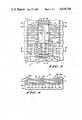
- FIG. 1shows a simplified plan view of a portion of a high frequency high power transistor assembly, according to the present invention, containing four transistor die;
- FIG. 2shows the same structure as in FIG. 1 but with a portion of the device input assembly containing the ballast resistors removed to show underlying details;
- FIG. 3is a cross-section in simplified schematic form of the assembly of FIG. 1;
- FIG. 4is a cross-section in simplified schematic form of a further cross-section of the assembly of FIG. 1.
- the transistor assembly illustrated hereinis shown as containing four transistor die electrically connected in parallel and having four ballast resistors, one per transistor die, in series with the input.
- the structure of the high frequency high power transistor assembly illustrated herein containing four such devices and four ballast resistorsis presented as an aid to understanding and not intended to be limiting, and that other arrangements embodying the same principles and die larger than zero (e.g. 2, 4, 6, 8, could equally well be used and arranged according to the teachings of the present invention.
- the inventionis particularly well suited to arrangements containing an even number of die, e.g. 2, 4, 6, 8, etc., but odd numbers of die greater than one could also be used.
- FIG. 1shows in simplified and schematic form a plan view of portion 9 of a high frequency high power transistor assembly according to the present invention.
- the parts of the assembly external to portion 9 and not shownconsist of the remainder of the package base, containing the mounting holes and the remaining length of the input and output leads. These are conventional.
- FIG. 2shows the same view of the assembly as in FIG. 1 but with certain portions removed to show details of the underlying structure.
- FIGS. 3-4show cross-sections in simplified and schematic form through various portions of the assembly of FIG. 1. The arrangement of parts making up the assembly of FIG. 1 is best understood by considering FIGS. 1-4 together.
- Assembly portion 9comprises metallic base or substrate 10 having recess 10c in which are mounted transistor die 12, ceramic isolators 13, and electrical input-output assembly 21 containing insulating piece or plate 16, metallization layers 17-19 and ballast resistors 20.
- Metal base 10may be of any material which is highly conductive both electrically and thermally.
- Gold plated OFHC copperis a convenient material for base 10, but other highly conductive materials could be used. Aluminum is an example of such an alternate material.
- Bottom 10e of recess 10cis substantially flat, although ridge 10d along the centerline of the cavity may be optionally used for convenience in aligning the internal parts.
- Electrically insulating pieces 13 and 16are desirably made of ceramic. Insulating pieces 13 should have the highest possible thermal conductivity.
- BeOis a suitable material for insulating pieces 13.
- Insulating piece or plate 16may be conveniently fabricated from any electrically insulating material having good RF properties.
- Al 2 O 3is a suitable material.
- Transistor die 12have contacts 14 on their upper surface, wherein contacts 14a are the electrical reference contacts and contacts 14b are the input contacts.
- Transistor die 12are of the type which have output contact 14c on their lower faces.
- Transistor die of this typeare well known in the art and include but are not limited to, for example, bipolar transistors, MOS transistors, and thyristors. Two terminal devices may also be employed, and as used herein, the term "transistor" is intended to include any devices having one or more top surface contacts and a bottom surface output contact.
- Transistor die 12are mounted on individual dielectric isolators 13, that is, transistor die 12a is mounted on individual isolator 13a, transistor die 12b on individual isolator 13b, transistor die 12c on individual isolator 13c, and transistor die 12d on individual isolator 13d. It is important that each transistor die be mounted on a separate isolator and that the mounting means be thermally highly conductive. It has been found that when two or more die are placed on the same isolator, that thicker isolators must be used and the thermal performances significantly degraded.
- die 12are mounted on the portion of isolators 13 which are adjacent to shoulders 10a-b of base 10. Die 12 are smaller than isolators 13. Thus, a portion of the upper surface of each isolator is not covered by die 12 and is available to support and to be bonded to input-output assembly 21.
- Input-output assembly 21comprises insulating plate 16 having input conductor 18, ballast resistors 20, and metal contacts 17 on its upper surface. Ceramic plate 16 has output conductor 19 with portion 19c on its lower surface bonded to portions 13g of conductors 13e on the upper surfaces of insulators 13, portion 19b extending around one end of insulating plate 16 and portion 19a on the upper surface, i.e., the same surface as input conductor 18.
- Input conductor 18is connected to input lead 11b via wire bonds 18a and output conductor 19 is connected to output lead 11a by wire bonds 19e.
- Leads 11a-bare mounted by insulating means 11c on base 10.
- insulating plates 13, 16, and insulating means 11c supporting leads 11a-bare shown cross-hatched in FIGS. 1-4. Ballast resistors 20 are stippled.
- Isolators 13are bonded to metallic base 10 by means 13f.
- Means 13fmust be a good thermal conductor but need not be electrically conducting.
- Upper surfaces 13u of isolators 13are covered with conductor layer 13e, typically a thin film of, for example, evaporated metal, to which are bonded output contacts 14c of transistor die 12.
- Portions 13g of upper surface conductor layers 13e on each of the several isolators 13extend under input assembly 21 and are bonded to conductor layer portion 19c of assembly 21.
- Input-output assembly 21provides for space efficient distribution of the input signal via input conductor 18 which extends centrally along cavity 10c of base 10 above the center line. Assembly 21 provides space for individual ballast resistor regions 20a-d, one each for each of transistor die 12a-d. Input conductor 18 is connected to input lead 11b via minimum length wire bonds 18a (see FIGS. 1 and 4). Ballast resistor regions 20a-d extend between input conductor 18 and contact regions 17, i.e. one each of ballast resistor regions 20a-d connected to contact regions 17a-d for each of transistor die 12a-d. Wire bonds 15 are used to make electrical contact to transistor die 12. Wire bonds 15b connect contacts 17 to input contacts 14b of transistor die 12, and wire bonds 15a connect reference contacts 14a of transistor die 12 to base 10 in shoulder regions 10a-b.
- FIG. 2is substantially similar to FIG. 1 except that the portion of electrical input-output assembly 21 at the top of the figure is cut away so that optional ridge 10d and portions 13g of metallization layers 13e on isolators 13a-b may be seen where they underly assembly 21.
- Base 10measures approximately 1 by 1.5 inches and has central cavity 10c approximately 0.625 inches square.
- Input lead 11b and output lead 11aare each approximately 0.5 inches in width.
- Isolators 13are formed from BeO pieces approximately 0.275 inches square and 25 mils thick.
- Semiconductor transistor diemeasuring approximately 0.25 inches by 0.13 are mounted on the isolators as shown in FIGS. 1-4.
- Insulating piece 16measures approximately 0.2 inches in width by approximately 0.55 inches in length and 0.025 inches in thickness and is formed from 96% alumina.
- Ballast resistors 17exhibit resistances typically of 1-3 ohms each, but smaller or larger values can be used, including zero.
- Substrate or base 10is approximately 0.2 inches thick.
- Cavity 10cis recessed approximately 0.06 inches into base 10.
- Isolators 13, chips 12, and input-output assembly 21are bonded together and to base 10 using a combination of soldering and eutectic bonding techniques well known in the art.
- soldering and eutectic bonding techniqueswell known in the art.
- Commercially available Au-Sn and Pb-In-Ag solder materials and pre-formsare suitable.
- a device assembly similar to that illustrated in FIGS. 1-4 and utilizing four N-channel enhancement mode RF field effect transistor diedelivers 600 watts of output power at 30 MHz at a power gain of 16 db (typical) with an efficiency of about 45 percent. Power gain decreases within increasing frequency but is still approximately 7.5 db at a frequency of 100 MHz with a power output of 600 watts. Water cooling is not used. These results are obtained with base 10 mounted on an air cooled copper heat sink. This performance exceeds that available from prior art devices. As compared to prior art devices or assemblies, fewer piece parts and internal connections are required. Higher power levels can be obtained by adding more die. High frequency operation can be obtained by using transistor die with finer geometries and greater emitter periphery so as to have lower parasitic capacity and greater gain-bandwidth product.
- the present inventionprovides a transistor assembly having improved power dissipation capabilities and high frequency performance, which uses fewer piece parts and is compactly arranged so that minimum lead length and minimum inductance bonds may be used to the external conductors. Further the number of welded or solder connections is reduced. In addition, the advantages and objectives described herein are achieved simultaneously.
Landscapes
- Engineering & Computer Science (AREA)
- Microelectronics & Electronic Packaging (AREA)
- Power Engineering (AREA)
- Computer Hardware Design (AREA)
- Physics & Mathematics (AREA)
- Condensed Matter Physics & Semiconductors (AREA)
- General Physics & Mathematics (AREA)
- Lead Frames For Integrated Circuits (AREA)
Abstract
Description
1. Field of the Invention
This invention relates in general to high frequency high power semiconductor devices and, more particularly, to high frequency high power transistor device assemblies having improved performance.
2. Background Art
High power high frequency semiconductor devices are widely used. In many circumstances it is essential that high power, i.e., in the range of several hundred watts, be provided at frequencies extending into the HF and VHF ranges (3-300 MHz) in a single device assembly. Most commonly, devices operating in these power and frequency ranges are fabricated from several semiconductor die operating electrically in parallel within a single housing or assembly.
In the prior art, devices capable of operating at power levels of approximately 500 watts at 2-30 MHz have been achieved. The type TH-20 transistor assembly manufacture by Thompson-CSF of Paris, France is a typical example. Higher power and higher frequency operation are much desired. Further, prior art devices have suffered from a number of limitations, in particular, poor thermal dissipation requiring the use of water cooled assemblies to carry away the heat, the use of large numbers of complex internal parts and the high cost thereof, the use of an excessive number of welded or solder internal connections which adversely affect the reliability of the unit, and the absence of chip-to-chip ballasting resistors to insure uniform current distribution in multi-chip designs. Thus, a need continues to exist for high frequency high power devices which will simultaneously achieve higher powers and higher operating frequencies, while avoiding water cooling and complex, expensive internal structures that need large numbers of welded or soldered connections, and which incorporate inter-chip ballasting resistors to equal chip currents.
Accordingly, it is an object of the present invention to provide an improved high power and high frequency semiconductor device assembly having power and frequency capabilities equal or greater than heretofor achieved.
It is an additional object of the present invention to provide an improved high power and high frequency device assembly in which the number of internal piece parts and the number of internal interconnections has been substantially reduced.
It is a further object of the present invention to provide an improved high frequency and high power device assembly in which the thermal performance is such as to eliminate the need for water cooling.
It is an additional object of the present invention to provide an improved high frequency and high power transistor assembly having a more compact internal arrangement so that lead length is minimized in order to achieve lower inductance.
It is a further object of the present invention to provide an improved high frequency and high power transistor assembly wherein the above advantages are achieved simultaneously.
As used herein the words "metal" or "metallic" are intended to refer to any highly electrically conductive material whether semiconductor, semimetal, intermetallic, or metal. The words "bond" or "bonding" are intended to refer to any metallurgical means for joining objects, including but not limited to soldering, eutectic bonding, brazing, or welding, and under circumstances where electrical conductivity is not required, the use of dielectric solders or adhesives such as but not limited solder glasses or epoxies. As used herein the words "wire bonds" are intended to refer to any form of interconnecting leads which extend in part above the surface to which they connect, whether round, flat, or tape mounted leads or incorporating bumps.
The attainment of the foregoing and other objects and advantages is achieved through the present invention wherein there is provided a high power high frequency transistor device, comprising: a metal base having a substantially flat bottomed recess therein; at least two insulating substrate isolators having metallized regions on their upper faces and mounted in the recess by their lower faces; at least two transistor die, smaller than the substrate isolators, each bonded to a first portion of the metallized region of one of the substrate isolators so to leave exposed a second portion of the metallized region, wherein the second portions of the metallized regions of the at least two substrate isolators are laterally adjacent to the centerline of the recess; and input-output connection means comprising an insulated base with substantially parallel upper and lower faces; wherein the input connection means has a first conductor region having a portion on the lower face bonded to the second portions of the metallized regions of the at least two substrate isolators and a portion on the upper face and an interconnecting portion therebetween; wherein input-output connection means has a second conductor region on the upper face separated from the first conductor region; and wherein the input-output connection means has third conductor regions on the upper face, one per transistor die, separated from the first and second conductor regions and electrically coupled to input leads of the transistor die; and wherein the input-output connection means has ballast resistor regions, one per transistor die, on the upper face connected between the second conductor region and the third conductor regions.
The metal base desirably forms the reference terminal of the device. Wide metal leads are mounted by insulating means on the metal base to form input and output connectons. Wire bonds are used to connect the input lead to the second conductor region on the upper face of the input-output connection means, and additional wire bonds are used to connect the output lead to the portion of the first conductor region lying on the upper face of the input-output connection means. Additional wire bonds are provided to connect the input contacts on the semiconductor die to the third conductor regions. The transistor die are desirably electrically connected in parallel. It is desirable that there be at least one ballast resistor region in series with each of the transistor die. Further wire bonds are provided to connect the reference terminals of the transistor die to the metal base. The output contact of each transistor die is located on the lower die surface and is bonded to the first portion of the metallized region of the substrate isolators. It is desirable that the flat bottom recess of the metal base have shoulders extending alongside the transistor die at a height substantially equal to the die surface to permit minimum length wire bonds connected to the reference contacts on the semiconductor transistor die. It is also desirable that the insulated external input and output leads on the metal base have upper surfaces at the perimeter of the recess which are substantially at the same elevation as the surface of the input-out connection means to permit minimum length wire bonds therebetween.
FIG. 1 shows a simplified plan view of a portion of a high frequency high power transistor assembly, according to the present invention, containing four transistor die;
FIG. 2 shows the same structure as in FIG. 1 but with a portion of the device input assembly containing the ballast resistors removed to show underlying details;
FIG. 3 is a cross-section in simplified schematic form of the assembly of FIG. 1; and
FIG. 4 is a cross-section in simplified schematic form of a further cross-section of the assembly of FIG. 1.
For purposes of explanation, the transistor assembly illustrated herein is shown as containing four transistor die electrically connected in parallel and having four ballast resistors, one per transistor die, in series with the input. However, those of skill in the art will understand that the structure of the high frequency high power transistor assembly illustrated herein containing four such devices and four ballast resistors is presented as an aid to understanding and not intended to be limiting, and that other arrangements embodying the same principles and die larger than zero (e.g. 2, 4, 6, 8, could equally well be used and arranged according to the teachings of the present invention. The invention is particularly well suited to arrangements containing an even number of die, e.g. 2, 4, 6, 8, etc., but odd numbers of die greater than one could also be used.
FIG. 1 shows in simplified and schematic form a plan view ofportion 9 of a high frequency high power transistor assembly according to the present invention. The parts of the assembly external toportion 9 and not shown consist of the remainder of the package base, containing the mounting holes and the remaining length of the input and output leads. These are conventional. FIG. 2 shows the same view of the assembly as in FIG. 1 but with certain portions removed to show details of the underlying structure. FIGS. 3-4 show cross-sections in simplified and schematic form through various portions of the assembly of FIG. 1. The arrangement of parts making up the assembly of FIG. 1 is best understood by considering FIGS. 1-4 together.
Transistor die 12 havecontacts 14 on their upper surface, whereincontacts 14a are the electrical reference contacts andcontacts 14b are the input contacts. Transistor die 12 are of the type which haveoutput contact 14c on their lower faces. Transistor die of this type are well known in the art and include but are not limited to, for example, bipolar transistors, MOS transistors, and thyristors. Two terminal devices may also be employed, and as used herein, the term "transistor" is intended to include any devices having one or more top surface contacts and a bottom surface output contact.
Transistor die 12 are mounted on individualdielectric isolators 13, that is, transistor die 12a is mounted onindividual isolator 13a, transistor die 12b onindividual isolator 13b, transistor die 12c onindividual isolator 13c, and transistor die 12d onindividual isolator 13d. It is important that each transistor die be mounted on a separate isolator and that the mounting means be thermally highly conductive. It has been found that when two or more die are placed on the same isolator, that thicker isolators must be used and the thermal performances significantly degraded.
As may be seen in FIG. 3, die 12 are mounted on the portion ofisolators 13 which are adjacent toshoulders 10a-b ofbase 10.Die 12 are smaller thanisolators 13. Thus, a portion of the upper surface of each isolator is not covered bydie 12 and is available to support and to be bonded to input-output assembly 21. Input-output assembly 21 comprises insulatingplate 16 havinginput conductor 18,ballast resistors 20, andmetal contacts 17 on its upper surface.Ceramic plate 16 hasoutput conductor 19 withportion 19c on its lower surface bonded toportions 13g ofconductors 13e on the upper surfaces ofinsulators 13,portion 19b extending around one end of insulatingplate 16 andportion 19a on the upper surface, i.e., the same surface asinput conductor 18.Input conductor 18 is connected to input lead 11b viawire bonds 18a andoutput conductor 19 is connected tooutput lead 11a bywire bonds 19e.Leads 11a-b are mounted by insulatingmeans 11c onbase 10. For convenience in understanding the drawings, insulatingplates means 11c supporting leads 11a-b are shown cross-hatched in FIGS. 1-4.Ballast resistors 20 are stippled.
Input-output assembly 21 provides for space efficient distribution of the input signal viainput conductor 18 which extends centrally alongcavity 10c ofbase 10 above the center line.Assembly 21 provides space for individual ballast resistor regions 20a-d, one each for each of transistor die 12a-d.Input conductor 18 is connected to input lead 11b via minimumlength wire bonds 18a (see FIGS. 1 and 4). Ballast resistor regions 20a-d extend betweeninput conductor 18 andcontact regions 17, i.e. one each of ballast resistor regions 20a-d connected to contact regions 17a-d for each of transistor die 12a-d.Wire bonds 15 are used to make electrical contact to transistor die 12.Wire bonds 15b connectcontacts 17 to inputcontacts 14b of transistor die 12, andwire bonds 15a connectreference contacts 14a of transistor die 12 tobase 10 inshoulder regions 10a-b.
FIG. 2 is substantially similar to FIG. 1 except that the portion of electrical input-output assembly 21 at the top of the figure is cut away so thatoptional ridge 10d andportions 13g ofmetallization layers 13e onisolators 13a-b may be seen where they underlyassembly 21.
A semiconductor device assembly conforming to the above described principles was constructed.Base 10 measures approximately 1 by 1.5 inches and hascentral cavity 10c approximately 0.625 inches square.Input lead 11b andoutput lead 11a are each approximately 0.5 inches in width.Isolators 13 are formed from BeO pieces approximately 0.275 inches square and 25 mils thick. Semiconductor transistor die measuring approximately 0.25 inches by 0.13 are mounted on the isolators as shown in FIGS. 1-4. Insulatingpiece 16 measures approximately 0.2 inches in width by approximately 0.55 inches in length and 0.025 inches in thickness and is formed from 96% alumina.Ballast resistors 17 exhibit resistances typically of 1-3 ohms each, but smaller or larger values can be used, including zero. Substrate orbase 10 is approximately 0.2 inches thick.Cavity 10c is recessed approximately 0.06 inches intobase 10.Isolators 13,chips 12, and input-output assembly 21 are bonded together and to base 10 using a combination of soldering and eutectic bonding techniques well known in the art. Commercially available Au-Sn and Pb-In-Ag solder materials and pre-forms are suitable.
A device assembly similar to that illustrated in FIGS. 1-4 and utilizing four N-channel enhancement mode RF field effect transistor die delivers 600 watts of output power at 30 MHz at a power gain of 16 db (typical) with an efficiency of about 45 percent. Power gain decreases within increasing frequency but is still approximately 7.5 db at a frequency of 100 MHz with a power output of 600 watts. Water cooling is not used. These results are obtained withbase 10 mounted on an air cooled copper heat sink. This performance exceeds that available from prior art devices. As compared to prior art devices or assemblies, fewer piece parts and internal connections are required. Higher power levels can be obtined by adding more die. High frequency operation can be obtained by using transistor die with finer geometries and greater emitter periphery so as to have lower parasitic capacity and greater gain-bandwidth product.
Having thus described the invention, it is apparent that the present invention provides a transistor assembly having improved power dissipation capabilities and high frequency performance, which uses fewer piece parts and is compactly arranged so that minimum lead length and minimum inductance bonds may be used to the external conductors. Further the number of welded or solder connections is reduced. In addition, the advantages and objectives described herein are achieved simultaneously.
While the invented structure has been illustrated in terms of a device assembly utilizing four transistor die, those of skill in the art will recognize that this is merely intended to be illustrative, and that the invented method can be used in combination with any number of transistors and/or with other semiconductor die as well. Accordingly, it is intended to include all such variations within the claims which follow.
Claims (4)
1. A high power, high frequency transistor unit, comprising:
an electrically and thermally conductive base plate having a centerline;
at least two separate electrically insulating but thermally conducting isolators disposed in either side of said centerline, each having a first principal face bonded to said base plate and a second principal face opposite said first principal face, wherein said second principal face has thereon a first metal layer;
at least two transistor die, each having a signal input contact, a reference contact, and a power output contact, wherein said signal input contact and said reference contact are on a first face of said transistor die and said power output contact is on an opposed second face of said transistor die, and wherein said at least two transistor die are disposed on said isolators, one per isolator, with said power output contact bonded to said first metal layer of said isolator;
a ballasted electrical input-output assembly comprising a substantially flat electrically insulating plate having first and second opposed principal faces, wherein said insulating plate extends over and parallel to said centerline and portions of said at least two isolators and bridges between at least two of said at least two isolators located on either side of said centerline;
wherein said insulating plate has on said first face a first metal region region forming an input lead for said assembly and at least two ballast resistor regions, one per transistor, each ballast resistor region being located between said input lead and a second metal region coupled to said input contact of one of said transistors;
wherein said insulating plate has on said second face an output conductor electrically coupled to said output contacts of said transistors die by said first metal layers on said isolators, and wherein said output conductor extends around an edge of said insulating plate onto said first surface; and
first wire bonds extending from said input lead to an external input lead of said assembly, second wire bonds extending from said output lead to an external output lead of said assembly, third wire bonds extending from said reference contacts of said transistor die to said substrate, and fourth wire bonds extending from said second metal regions on said insulating plate to said input contacts of said transistor die.
2. A high power, high frequency transistor device, comprising:
a metal base having a substantially flat bottomed recess therein;
at least two insulating substrate isolators having metallized regions on their upper faces and mounted in said recess by their lower faces;
at least two transistor die, smaller than said substrate isolators, each bonded to a first portion of said metallized region of one of said substrate isolators so as to leave exposed a second portion of said metallized region, wherein said second portions of said metallized regions of said at least two substrate isolators are laterally adjacent; and
connection means comprising an insulating base with substantially parallel upper and lower faces, with a first conductor region having a portion on said lower face bonded to said second portions of said metallized regions of said substrate isolators and a portion on said upper face and an interconnecting portion therebetween, with a second conductor region on said upper face separated from said first conductor region, and with ballast resistor regions, one per transistor die on said first face connected to said second conductor region and coupled to said transistor die.
3. A high power semiconductor device assembly comprising:
a metal base having a substantially flat bottomed recess therein;
at least two insulating substrate isolators having metallized regions on their upper faces and mounted in said recess by their lower faces;
at least two semiconductor die, smaller than said substrate isolators, wherein an upper face of each die contains an input contact and a lower face of each die contains an output contact, and wherein said output contact is directly bonded to a first portion of said metallized region of one of said substrate isolators so as to leave exposed a second portion of said metallized region, and wherein said second portions of said metallized regions of said at least two substrate isolators are laterally adjacent; and
connection means comprising an insulating base with substantially parallel upper and lower faces, with a first conductor region having a portion on said lower face bonded to said second portions of said metallized regions of said substrate isolators and a portion on said upper face and an interconnecting portion therebetween, and with a second conductor region on said upper face separated from said first conductor region and electrically coupled to said input contact of said die.
4. A high power semiconductor device assembly comprising:
a metal base having a substantially flat bottomed recess therein;
at least two insulating substrate isolators having metallized regions on their upper faces and mounted in said recess by their lower faces;
at least two semiconductor die, smaller than said substrate isolators, wherein an upper face of each die contains an input contact and a lower face of each die contains an output contact, and wherein said output contact is directly bonded to a first portion of said metallized region of one of said substrate isolators so as to leave exposed a second portion of said metallized region, and wherein said second portions of said metallized regions of said at least two substrate isolators are laterally adjacent; and
connection means comprising an insulating base with substantially parallel upper and lower faces, with a first conductor region having a portion on said lower face bonded to said second portions of said metallized regions of said substrate isolators and a portion on said upper face and an interconnecting portion therebetween.
Priority Applications (1)
| Application Number | Priority Date | Filing Date | Title |
|---|---|---|---|
| US06/820,773US4639760A (en) | 1986-01-21 | 1986-01-21 | High power RF transistor assembly |
Applications Claiming Priority (1)
| Application Number | Priority Date | Filing Date | Title |
|---|---|---|---|
| US06/820,773US4639760A (en) | 1986-01-21 | 1986-01-21 | High power RF transistor assembly |
Publications (1)
| Publication Number | Publication Date |
|---|---|
| US4639760Atrue US4639760A (en) | 1987-01-27 |
Family
ID=25231690
Family Applications (1)
| Application Number | Title | Priority Date | Filing Date |
|---|---|---|---|
| US06/820,773Expired - LifetimeUS4639760A (en) | 1986-01-21 | 1986-01-21 | High power RF transistor assembly |
Country Status (1)
| Country | Link |
|---|---|
| US (1) | US4639760A (en) |
Cited By (42)
| Publication number | Priority date | Publication date | Assignee | Title |
|---|---|---|---|---|
| GB2199988A (en)* | 1987-01-12 | 1988-07-20 | Intel Corp | Multi-layer molded plastic ic package |
| US4816422A (en)* | 1986-12-29 | 1989-03-28 | General Electric Company | Fabrication of large power semiconductor composite by wafer interconnection of individual devices |
| US4835120A (en)* | 1987-01-12 | 1989-05-30 | Debendra Mallik | Method of making a multilayer molded plastic IC package |
| US4891687A (en)* | 1987-01-12 | 1990-01-02 | Intel Corporation | Multi-layer molded plastic IC package |
| US4914045A (en)* | 1985-12-19 | 1990-04-03 | Teccor Electronics, Inc. | Method of fabricating packaged TRIAC and trigger switch |
| EP0441180A1 (en)* | 1989-01-09 | 1991-08-14 | Mitsubishi Denki Kabushiki Kaisha | Integrated circuits containing microwave circuits |
| EP0434264A3 (en)* | 1989-12-22 | 1991-12-18 | Westinghouse Electric Corporation | Heat dissipation method and package for power semiconductor components |
| DE4120427A1 (en)* | 1990-06-20 | 1992-01-23 | Mitsubishi Electric Corp | DISCHARGE-EXTENDED LASER DEVICE |
| US5105260A (en)* | 1989-10-31 | 1992-04-14 | Sgs-Thomson Microelectronics, Inc. | Rf transistor package with nickel oxide barrier |
| US5109268A (en)* | 1989-12-29 | 1992-04-28 | Sgs-Thomson Microelectronics, Inc. | Rf transistor package and mounting pad |
| DE4131949A1 (en)* | 1990-09-25 | 1992-04-30 | Mitsubishi Electric Corp | SWITCHING DEVICE FOR LASER DEVICES |
| US5136271A (en)* | 1989-01-09 | 1992-08-04 | Mitsubishi Denki Kabushiki Kaisha | Microwave integrated circuit mountings |
| US5210439A (en)* | 1988-01-30 | 1993-05-11 | Robert Bosch Gmbh | Power transistor monolithic integrated structure |
| US5258646A (en)* | 1990-11-16 | 1993-11-02 | Mitsubishi Denki Kabushiki Kaisha | Package for microwave IC |
| EP0579293A1 (en)* | 1989-07-14 | 1994-01-19 | Motorola, Inc. | Hybrid amplifier |
| US5455448A (en)* | 1992-09-03 | 1995-10-03 | Sgs-Thomson Microelectronics, Inc. | Bipolar, monolithic, high-power RF transistor with isolated top collector |
| US5455453A (en)* | 1991-07-01 | 1995-10-03 | Sumitomo Electric Industries, Ltd. | Plastic package type semiconductor device having a rolled metal substrate |
| US5760473A (en)* | 1996-06-25 | 1998-06-02 | Brush Wellman Inc. | Semiconductor package having a eutectic bonding layer |
| US5777259A (en)* | 1994-01-14 | 1998-07-07 | Brush Wellman Inc. | Heat exchanger assembly and method for making the same |
| US5777384A (en)* | 1996-10-11 | 1998-07-07 | Motorola, Inc. | Tunable semiconductor device |
| US5869893A (en)* | 1993-12-03 | 1999-02-09 | Seiko Instruments Inc. | Semiconductor device having a trapezoidal joint chip |
| US6022426A (en)* | 1995-05-31 | 2000-02-08 | Brush Wellman Inc. | Multilayer laminate process |
| US6056186A (en)* | 1996-06-25 | 2000-05-02 | Brush Wellman Inc. | Method for bonding a ceramic to a metal with a copper-containing shim |
| US6291878B1 (en) | 1993-04-22 | 2001-09-18 | Sundstrand Corporation | Package for multiple high power electrical components |
| US20030100197A1 (en)* | 2001-11-26 | 2003-05-29 | Powerwave Technologies, Inc. | Edge-plated well for circuit board components |
| US20030141587A1 (en)* | 2002-01-29 | 2003-07-31 | Advanced Power Technology, Inc., A Delaware Corporation | Split-gate power module and method for suppressing oscillation therein |
| US20040104489A1 (en)* | 2001-03-28 | 2004-06-03 | International Rectifier Corporation | Direct fet device for high frequency application |
| US20050269677A1 (en)* | 2004-05-28 | 2005-12-08 | Martin Standing | Preparation of front contact for surface mounting |
| US20060091512A1 (en)* | 2004-11-01 | 2006-05-04 | Mitsubishi Denki Kabushiki Kaisha | Semiconductor device and manufacturing process thereof |
| US20060220123A1 (en)* | 2000-04-04 | 2006-10-05 | International Rectifier Corporation | Chip scale surface mounted device and process of manufacture |
| US20060240598A1 (en)* | 2005-04-20 | 2006-10-26 | International Rectifier Corporation | Chip scale package |
| US20060249836A1 (en)* | 2005-04-22 | 2006-11-09 | Andy Farlow | Chip-scale package |
| US20070012947A1 (en)* | 2002-07-15 | 2007-01-18 | International Rectifier Corporation | Direct FET device for high frequency application |
| US20070096297A1 (en)* | 2005-09-21 | 2007-05-03 | Frey Richard B | RF power transistor package |
| US20080157310A1 (en)* | 2006-12-29 | 2008-07-03 | Fairchild Korea Semiconductor, Ltd. | Power device package |
| US20080197473A1 (en)* | 2007-02-16 | 2008-08-21 | Taiwan Semiconductor Manufacturing Co., Ltd. | Chip holder with wafer level redistribution layer |
| US20080246127A1 (en)* | 2002-07-15 | 2008-10-09 | International Rectifier Corporation | Arrangement for high frequency application |
| USRE41559E1 (en) | 2001-10-10 | 2010-08-24 | International Rectifier Corporation | Semiconductor device package with improved cooling |
| US20100237467A1 (en)* | 2009-03-18 | 2010-09-23 | International Business Machines Corporation | Interconnect Structures, Methods for Fabricating Interconnect Structures, and Design Structures for a Radiofrequency Integrated Circuit |
| US8061023B2 (en) | 2005-04-21 | 2011-11-22 | International Rectifier Corporation | Process of fabricating a semiconductor package |
| US20180166356A1 (en)* | 2016-12-13 | 2018-06-14 | Globalfoundries Inc. | Fan-out circuit packaging with integrated lid |
| CN113272954A (en)* | 2018-12-04 | 2021-08-17 | 克里公司 | Packaged transistor device with input-output isolation and method of forming packaged transistor device with input-output isolation |
Citations (6)
| Publication number | Priority date | Publication date | Assignee | Title |
|---|---|---|---|---|
| US4038677A (en)* | 1974-02-22 | 1977-07-26 | Robert Bosch G.M.B.H. | Composite semiconductor unit and method |
| DE2806099A1 (en)* | 1977-02-17 | 1978-08-24 | Varian Associates | SEMICONDUCTOR ASSEMBLY |
| JPS5889852A (en)* | 1981-11-24 | 1983-05-28 | Nec Corp | Semiconductor device |
| US4408219A (en)* | 1979-11-21 | 1983-10-04 | Thomson-Csf | Device for connecting in parallel power transistors in very high frequency |
| JPS5935456A (en)* | 1982-08-23 | 1984-02-27 | Nec Corp | Semiconductor device |
| US4518982A (en)* | 1981-02-27 | 1985-05-21 | Motorola, Inc. | High current package with multi-level leads |
- 1986
- 1986-01-21USUS06/820,773patent/US4639760A/ennot_activeExpired - Lifetime
Patent Citations (6)
| Publication number | Priority date | Publication date | Assignee | Title |
|---|---|---|---|---|
| US4038677A (en)* | 1974-02-22 | 1977-07-26 | Robert Bosch G.M.B.H. | Composite semiconductor unit and method |
| DE2806099A1 (en)* | 1977-02-17 | 1978-08-24 | Varian Associates | SEMICONDUCTOR ASSEMBLY |
| US4408219A (en)* | 1979-11-21 | 1983-10-04 | Thomson-Csf | Device for connecting in parallel power transistors in very high frequency |
| US4518982A (en)* | 1981-02-27 | 1985-05-21 | Motorola, Inc. | High current package with multi-level leads |
| JPS5889852A (en)* | 1981-11-24 | 1983-05-28 | Nec Corp | Semiconductor device |
| JPS5935456A (en)* | 1982-08-23 | 1984-02-27 | Nec Corp | Semiconductor device |
Cited By (71)
| Publication number | Priority date | Publication date | Assignee | Title |
|---|---|---|---|---|
| US4914045A (en)* | 1985-12-19 | 1990-04-03 | Teccor Electronics, Inc. | Method of fabricating packaged TRIAC and trigger switch |
| US4816422A (en)* | 1986-12-29 | 1989-03-28 | General Electric Company | Fabrication of large power semiconductor composite by wafer interconnection of individual devices |
| US4835120A (en)* | 1987-01-12 | 1989-05-30 | Debendra Mallik | Method of making a multilayer molded plastic IC package |
| US4891687A (en)* | 1987-01-12 | 1990-01-02 | Intel Corporation | Multi-layer molded plastic IC package |
| GB2199988B (en)* | 1987-01-12 | 1990-04-25 | Intel Corp | Multi-layer molded plastic ic package |
| GB2199988A (en)* | 1987-01-12 | 1988-07-20 | Intel Corp | Multi-layer molded plastic ic package |
| US5210439A (en)* | 1988-01-30 | 1993-05-11 | Robert Bosch Gmbh | Power transistor monolithic integrated structure |
| US5136271A (en)* | 1989-01-09 | 1992-08-04 | Mitsubishi Denki Kabushiki Kaisha | Microwave integrated circuit mountings |
| EP0441180A1 (en)* | 1989-01-09 | 1991-08-14 | Mitsubishi Denki Kabushiki Kaisha | Integrated circuits containing microwave circuits |
| EP0579293A1 (en)* | 1989-07-14 | 1994-01-19 | Motorola, Inc. | Hybrid amplifier |
| US5105260A (en)* | 1989-10-31 | 1992-04-14 | Sgs-Thomson Microelectronics, Inc. | Rf transistor package with nickel oxide barrier |
| USRE37082E1 (en) | 1989-10-31 | 2001-03-06 | Stmicroelectronics, Inc. | RF transistor package with nickel oxide barrier |
| EP0434264A3 (en)* | 1989-12-22 | 1991-12-18 | Westinghouse Electric Corporation | Heat dissipation method and package for power semiconductor components |
| US5814880A (en)* | 1989-12-22 | 1998-09-29 | Northrop Grumman Corporation | Thick film copper metallization for microwave power transistor packages |
| US5109268A (en)* | 1989-12-29 | 1992-04-28 | Sgs-Thomson Microelectronics, Inc. | Rf transistor package and mounting pad |
| USRE35845E (en)* | 1989-12-29 | 1998-07-14 | Sgs-Thomson Microelectronics, Inc. | RF transistor package and mounting pad |
| DE4120427A1 (en)* | 1990-06-20 | 1992-01-23 | Mitsubishi Electric Corp | DISCHARGE-EXTENDED LASER DEVICE |
| DE4120427C2 (en)* | 1990-06-20 | 1996-10-17 | Mitsubishi Electric Corp | Discharge-excited laser devices |
| DE4131949A1 (en)* | 1990-09-25 | 1992-04-30 | Mitsubishi Electric Corp | SWITCHING DEVICE FOR LASER DEVICES |
| US5305338A (en)* | 1990-09-25 | 1994-04-19 | Mitsubishi Denki Kabushiki Kaisha | Switch device for laser |
| DE4131949C2 (en)* | 1990-09-25 | 1996-10-10 | Mitsubishi Electric Corp | Switching devices for a discharge-excited pulse laser device |
| US5258646A (en)* | 1990-11-16 | 1993-11-02 | Mitsubishi Denki Kabushiki Kaisha | Package for microwave IC |
| US5455453A (en)* | 1991-07-01 | 1995-10-03 | Sumitomo Electric Industries, Ltd. | Plastic package type semiconductor device having a rolled metal substrate |
| US5643834A (en)* | 1991-07-01 | 1997-07-01 | Sumitomo Electric Industries, Ltd. | Process for manufacturing a semiconductor substrate comprising laminated copper, silicon oxide and silicon nitride layers |
| US5455448A (en)* | 1992-09-03 | 1995-10-03 | Sgs-Thomson Microelectronics, Inc. | Bipolar, monolithic, high-power RF transistor with isolated top collector |
| US6291878B1 (en) | 1993-04-22 | 2001-09-18 | Sundstrand Corporation | Package for multiple high power electrical components |
| US5869893A (en)* | 1993-12-03 | 1999-02-09 | Seiko Instruments Inc. | Semiconductor device having a trapezoidal joint chip |
| US5777259A (en)* | 1994-01-14 | 1998-07-07 | Brush Wellman Inc. | Heat exchanger assembly and method for making the same |
| US6022426A (en)* | 1995-05-31 | 2000-02-08 | Brush Wellman Inc. | Multilayer laminate process |
| US6056186A (en)* | 1996-06-25 | 2000-05-02 | Brush Wellman Inc. | Method for bonding a ceramic to a metal with a copper-containing shim |
| US5760473A (en)* | 1996-06-25 | 1998-06-02 | Brush Wellman Inc. | Semiconductor package having a eutectic bonding layer |
| US5777384A (en)* | 1996-10-11 | 1998-07-07 | Motorola, Inc. | Tunable semiconductor device |
| US20060220123A1 (en)* | 2000-04-04 | 2006-10-05 | International Rectifier Corporation | Chip scale surface mounted device and process of manufacture |
| US7476979B2 (en) | 2000-04-04 | 2009-01-13 | International Rectifier Corporation | Chip scale surface mounted device and process of manufacture |
| US20040104489A1 (en)* | 2001-03-28 | 2004-06-03 | International Rectifier Corporation | Direct fet device for high frequency application |
| US7119447B2 (en)* | 2001-03-28 | 2006-10-10 | International Rectifier Corporation | Direct fet device for high frequency application |
| USRE41559E1 (en) | 2001-10-10 | 2010-08-24 | International Rectifier Corporation | Semiconductor device package with improved cooling |
| US6818477B2 (en) | 2001-11-26 | 2004-11-16 | Powerwave Technologies, Inc. | Method of mounting a component in an edge-plated hole formed in a printed circuit board |
| US20030100197A1 (en)* | 2001-11-26 | 2003-05-29 | Powerwave Technologies, Inc. | Edge-plated well for circuit board components |
| US20050218500A1 (en)* | 2002-01-29 | 2005-10-06 | Advanced Power Technology, Inc., A Delaware Corporation | Split-gate power module for suppressing oscillation therein |
| US6939743B2 (en) | 2002-01-29 | 2005-09-06 | Advanced Power Technology, Inc. | Split-gate power module and method for suppressing oscillation therein |
| US7342262B2 (en) | 2002-01-29 | 2008-03-11 | Microsemi Corporation | Split-gate power module for suppressing oscillation therein |
| US20030141587A1 (en)* | 2002-01-29 | 2003-07-31 | Advanced Power Technology, Inc., A Delaware Corporation | Split-gate power module and method for suppressing oscillation therein |
| US20080246127A1 (en)* | 2002-07-15 | 2008-10-09 | International Rectifier Corporation | Arrangement for high frequency application |
| US7579697B2 (en)* | 2002-07-15 | 2009-08-25 | International Rectifier Corporation | Arrangement for high frequency application |
| US20070012947A1 (en)* | 2002-07-15 | 2007-01-18 | International Rectifier Corporation | Direct FET device for high frequency application |
| US7397137B2 (en)* | 2002-07-15 | 2008-07-08 | International Rectifier Corporation | Direct FET device for high frequency application |
| US20050269677A1 (en)* | 2004-05-28 | 2005-12-08 | Martin Standing | Preparation of front contact for surface mounting |
| US20060091512A1 (en)* | 2004-11-01 | 2006-05-04 | Mitsubishi Denki Kabushiki Kaisha | Semiconductor device and manufacturing process thereof |
| US7642640B2 (en)* | 2004-11-01 | 2010-01-05 | Mitsubishi Denki Kabushiki Kaisha | Semiconductor device and manufacturing process thereof |
| US20090174058A1 (en)* | 2005-04-20 | 2009-07-09 | International Rectifier Corporation | Chip scale package |
| US8097938B2 (en) | 2005-04-20 | 2012-01-17 | International Rectifier Corporation | Conductive chip-scale package |
| US7524701B2 (en) | 2005-04-20 | 2009-04-28 | International Rectifier Corporation | Chip-scale package |
| US20060240598A1 (en)* | 2005-04-20 | 2006-10-26 | International Rectifier Corporation | Chip scale package |
| US9799623B2 (en) | 2005-04-21 | 2017-10-24 | Infineon Technologies Americas Corp. | Semiconductor package with conductive clip |
| US8061023B2 (en) | 2005-04-21 | 2011-11-22 | International Rectifier Corporation | Process of fabricating a semiconductor package |
| US8466546B2 (en) | 2005-04-22 | 2013-06-18 | International Rectifier Corporation | Chip-scale package |
| US20060249836A1 (en)* | 2005-04-22 | 2006-11-09 | Andy Farlow | Chip-scale package |
| US7569927B2 (en) | 2005-09-21 | 2009-08-04 | Microsemi Corporation | RF power transistor package |
| US7956455B2 (en) | 2005-09-21 | 2011-06-07 | Microsemi Corporation | RF power transistor package |
| US20090261471A1 (en)* | 2005-09-21 | 2009-10-22 | Microsemi Corporation | Rf power transistor package |
| US20070096297A1 (en)* | 2005-09-21 | 2007-05-03 | Frey Richard B | RF power transistor package |
| US7800224B2 (en)* | 2006-12-29 | 2010-09-21 | Fairchild Korea Semiconductor, Ltd. | Power device package |
| US20080157310A1 (en)* | 2006-12-29 | 2008-07-03 | Fairchild Korea Semiconductor, Ltd. | Power device package |
| US8049323B2 (en)* | 2007-02-16 | 2011-11-01 | Taiwan Semiconductor Manufacturing Co., Ltd. | Chip holder with wafer level redistribution layer |
| US20080197473A1 (en)* | 2007-02-16 | 2008-08-21 | Taiwan Semiconductor Manufacturing Co., Ltd. | Chip holder with wafer level redistribution layer |
| US20100237467A1 (en)* | 2009-03-18 | 2010-09-23 | International Business Machines Corporation | Interconnect Structures, Methods for Fabricating Interconnect Structures, and Design Structures for a Radiofrequency Integrated Circuit |
| US8298902B2 (en) | 2009-03-18 | 2012-10-30 | International Business Machines Corporation | Interconnect structures, methods for fabricating interconnect structures, and design structures for a radiofrequency integrated circuit |
| US8791545B2 (en) | 2009-03-18 | 2014-07-29 | International Business Machines Corporation | Interconnect structures and design structures for a radiofrequency integrated circuit |
| US20180166356A1 (en)* | 2016-12-13 | 2018-06-14 | Globalfoundries Inc. | Fan-out circuit packaging with integrated lid |
| CN113272954A (en)* | 2018-12-04 | 2021-08-17 | 克里公司 | Packaged transistor device with input-output isolation and method of forming packaged transistor device with input-output isolation |
Similar Documents
| Publication | Publication Date | Title |
|---|---|---|
| US4639760A (en) | High power RF transistor assembly | |
| US5637922A (en) | Wireless radio frequency power semiconductor devices using high density interconnect | |
| US5075759A (en) | Surface mounting semiconductor device and method | |
| KR100367936B1 (en) | High frequency integrated circuit device with laminated body | |
| US5170337A (en) | Low-inductance package for multiple paralleled devices operating at high frequency | |
| US4649416A (en) | Microwave transistor package | |
| US3986196A (en) | Through-substrate source contact for microwave FET | |
| US5532512A (en) | Direct stacked and flip chip power semiconductor device structures | |
| JP5290963B2 (en) | Basic elements for high-efficiency double-sided cooling discrete power packages, especially for innovative power modules | |
| EP0115000B1 (en) | Power chip package | |
| US20020163070A1 (en) | High frequency power device with a plastic molded package and direct bonded substrate | |
| US20020014694A1 (en) | Capsule for semiconductor components | |
| US5708283A (en) | Flip chip high power monolithic integrated circuit thermal bumps | |
| US6255672B1 (en) | Semiconductor device | |
| US7285866B2 (en) | Surface mounted package with die bottom spaced from support board | |
| US5463250A (en) | Semiconductor component package | |
| US5406120A (en) | Hermetically sealed semiconductor ceramic package | |
| US3728589A (en) | Semiconductor assembly | |
| JP2001502845A (en) | RF power package with double grounding | |
| US5126827A (en) | Semiconductor chip header having particular surface metallization | |
| JP2000049281A (en) | Semiconductor device | |
| JPH09321216A (en) | Power semiconductor device | |
| JPH0563454A (en) | Semiconductor device | |
| EP0408904A2 (en) | Surface mounting semiconductor device and method | |
| JPH09213730A (en) | High-frequency module substrate and high-frequency power amplification module having it |
Legal Events
| Date | Code | Title | Description |
|---|---|---|---|
| AS | Assignment | Owner name:MOTOROLA, INC., SCHAUMBURG, IL., A CORP. OF DE. Free format text:ASSIGNMENT OF ASSIGNORS INTEREST.;ASSIGNORS:GRANBERG, HELGE O.;COFFMAN, SAMUEL L.;REEL/FRAME:004508/0897 Effective date:19860121 | |
| STCF | Information on status: patent grant | Free format text:PATENTED CASE | |
| FPAY | Fee payment | Year of fee payment:4 | |
| FPAY | Fee payment | Year of fee payment:8 | |
| FPAY | Fee payment | Year of fee payment:12 | |
| AS | Assignment | Owner name:FREESCALE SEMICONDUCTOR, INC., TEXAS Free format text:ASSIGNMENT OF ASSIGNORS INTEREST;ASSIGNOR:MOTOROLA, INC.;REEL/FRAME:015698/0657 Effective date:20040404 Owner name:FREESCALE SEMICONDUCTOR, INC.,TEXAS Free format text:ASSIGNMENT OF ASSIGNORS INTEREST;ASSIGNOR:MOTOROLA, INC.;REEL/FRAME:015698/0657 Effective date:20040404 |