US4638310A - Method of addressing liquid crystal displays - Google Patents
Method of addressing liquid crystal displaysDownload PDFInfo
- Publication number
- US4638310A US4638310AUS06/647,567US64756784AUS4638310AUS 4638310 AUS4638310 AUS 4638310AUS 64756784 AUS64756784 AUS 64756784AUS 4638310 AUS4638310 AUS 4638310A
- Authority
- US
- United States
- Prior art keywords
- pulse
- strobing
- waveform
- polarity
- duration
- Prior art date
- Legal status (The legal status is an assumption and is not a legal conclusion. Google has not performed a legal analysis and makes no representation as to the accuracy of the status listed.)
- Expired - Fee Related
Links
Images


Classifications
- G—PHYSICS
- G09—EDUCATION; CRYPTOGRAPHY; DISPLAY; ADVERTISING; SEALS
- G09G—ARRANGEMENTS OR CIRCUITS FOR CONTROL OF INDICATING DEVICES USING STATIC MEANS TO PRESENT VARIABLE INFORMATION
- G09G3/00—Control arrangements or circuits, of interest only in connection with visual indicators other than cathode-ray tubes
- G09G3/20—Control arrangements or circuits, of interest only in connection with visual indicators other than cathode-ray tubes for presentation of an assembly of a number of characters, e.g. a page, by composing the assembly by combination of individual elements arranged in a matrix no fixed position being assigned to or needed to be assigned to the individual characters or partial characters
- G09G3/34—Control arrangements or circuits, of interest only in connection with visual indicators other than cathode-ray tubes for presentation of an assembly of a number of characters, e.g. a page, by composing the assembly by combination of individual elements arranged in a matrix no fixed position being assigned to or needed to be assigned to the individual characters or partial characters by control of light from an independent source
- G09G3/36—Control arrangements or circuits, of interest only in connection with visual indicators other than cathode-ray tubes for presentation of an assembly of a number of characters, e.g. a page, by composing the assembly by combination of individual elements arranged in a matrix no fixed position being assigned to or needed to be assigned to the individual characters or partial characters by control of light from an independent source using liquid crystals
- G09G3/3611—Control of matrices with row and column drivers
- G09G3/3622—Control of matrices with row and column drivers using a passive matrix
- G09G3/3629—Control of matrices with row and column drivers using a passive matrix using liquid crystals having memory effects, e.g. ferroelectric liquid crystals
- G—PHYSICS
- G09—EDUCATION; CRYPTOGRAPHY; DISPLAY; ADVERTISING; SEALS
- G09G—ARRANGEMENTS OR CIRCUITS FOR CONTROL OF INDICATING DEVICES USING STATIC MEANS TO PRESENT VARIABLE INFORMATION
- G09G2310/00—Command of the display device
- G09G2310/06—Details of flat display driving waveforms
- G09G2310/061—Details of flat display driving waveforms for resetting or blanking
Definitions
- This inventionrelates to a method of addressing matrix array type ferro-electric liquid crystal display devices.
- Hitherto dynamic scattering mode liquid crystal display deviceshave been operated using a d.c. drive or an a.c. one
- field effect mode liquid crystal deviceshave generally been operated using an a.c. drive in order to avoid performance impairment problems associated with electrolytic degradation of the liquid crystal layer.
- Such deviceshave employed liquid crystals that do not exhibit ferro-electricity, and the material interacts with an applied electric field by way of an induced dipole. As a result they are not sensitive to the polarity of the applied field, but respond to the applied RMS voltage averaged over approximately one response time at that voltage. There may also be frequency dependence as in the case of so-called two-frequency materials, but this only affects the type of response produced by the applied field.
- ferro-electric liquid crystalexhibits a permanent electric dipole, and it is this permanent dipole which will interact with an applied electric field.
- Ferro-electric liquid crystalsare of interest in display applications because they are expected to show a greater coupling with an applied field than that typical of a liquid crystal that relies on coupling with an induced dipole, and hence ferro-electric liquid crystals are expected to show a faster response.
- a ferro-electric liquid crystal display modeis described for instance by N. A. Clark et al. in a paper entitled "Ferro-electric Liquid Crystal Electro-Optics Using the Surface Stabilized Structure" appearing in Mol. Cryst. Liq. Cryst. 1983. Volume 94, pages 213 to 234.
- ferro-electricsTwo properties of ferro-electrics set the problems of matrix addressing such devices apart from the addressing of non-ferro-electric devices. First they are polarity sensitive, and second their response times exhibit a relatively weak dependence upon applied voltage. The response time of a ferro-electric is typically proportional to the inverse square of applied voltage, or even worse, proportional to the inverse single power of voltage; whereas a non-ferro-electric smectic A, which in certain other respects is a comparable device exhibiting long term storage capability, exhibits a response time that is typically proportional to the inverse fifth power of voltage.
- a good drive scheme for addressing a ferro-electric liquid crystal displaymust keep to a minimum the incidence of wrong polarity signals to any given pixel, whether it is intended as an ON pixel or an OFF pixel.
- a method of addressing a matrix array type liquid crystal display device with a ferro-electric liquid crystal layer whose pixels are defined by the areas of overlay between the members of a first set of electrodes on one side of the liquid crystal layer and the members of a second set of electrodes on the other side of the layerwherein strobing pulses are applied serially to the members of the first set while data pulses are applied in parallel to the second set in order to address the cell line by line, and wherein the waveform of a data pulse is balanced bipolar and twice the duration of a strobing pulse.
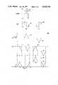
- FIGS. 1 to 3depict the waveforms associated with three alternative addressing schemes contemplated by the present invention.
- All three of the addressing schemes contemplated by the present inventionaddress a display on a line by line basis using a parallel input of data pulses on a set of column electrodes while a strobing pulse is applied to each of the row electrodes in turn.
- the strobe pulse voltage waveform 10is a unidirectional pulse of height V s and duration t.
- An ON data pulse voltage waveform 11ais a balanced bipolar pulse making an excursion to -V D for a time t and then an excursion to +V D for a further time t.
- An OFF data pulse waveform 11bis the inverse of the ON data pulse waveform.
- Any given pixelwhich is defined by the area of intersection of a particular row electrode with a particular column electrode, will receive a succession of data pulses that address other pixels in the same column.
- the first half of an ON data pulsewill tend to drive that pixel a little way towards the ON state, and then the second half will tend to drive it the same amount in the reverse direction and thus restore the status quo.
- This effectis depicted at 12a.
- the effect of an OFF data pulseis first to tend to drive the pixel towards the OFF state, and then to restore the original state as depicted at 12b.
- the effect of ON data pulsesis to drive the pixel a little way towards the ON state, and then restore the saturated OFF state, as depicted at 14a.
- the first OFF data pulseintroduces a difference because the first half of such a pulse cannot drive the saturated OFF pixel any further OFF.
- the resultis that at the end of the first OFF pulse a pixel previously in a fully saturated OFF state is driven a small amount ON, as depicted at 14b. Thereafter that pixel will make further temporary excursions either back to the fully OFF state, as depicted at 15b, or to a state that is slightly further ON, as depicted at 15a.
- there is no staircase effectbecause both types of data pulse end up by restoring the state that existed before commencement of the data pulse.
- the fully ON stateis depicted at 16, and it is seen that here there is an analogous situation, with the first ON data pulse driving the pixel a small amount OFF, as depicted at 17a. With any data pulse after the first ON data pulse, the pixel always comes to rest at this level at the end of the data pulse irrespective of whether the data pulse is an ON or an OFF pulse, as depicted at 18a and 18b.
- the strobe pulsecoincides with the first half of the data pulse, and hence the combined effect in the first half of the data pulse is the application of a voltage of (V S +V D ) tending to turn the pixel ON. Then, in the second half of the data pulse, there is a voltage V D tending to turn the pixel OFF.
- V S +V Da voltage tending to turn the pixel ON.
- V Da voltage tending to turn the pixel OFF.
- the ON voltage duration tdivided by the response time at that voltage T.sub.(V.sbsb.S +V .sbsb.D.sub.
- FIG. 1Inspection of FIG. 1 reveals that if the strobing pulse is synchronized with the second halves of the data pulses instead of with their first halves, substantially the same situation prevails, though the roles of the data pulse waveforms are interchanged.
- This first addressing schemeuses a unidirectional strobing pulse for data entry, and so it does not of itself permit the use of the data pulses to set some pixels into the ON state while at the same time setting others into the OFF state. Therefore, it is necessary to blank the cell before addressing.
- Thiscan be done on a line-by-line basis by inserting a blanking pulse of opposite polarity to the strobing pulse onto the row electrode in the time interval terminating with the commencement of data entry for that row, and starting with the commencement of the data entry for the preceding line.
- blankingcan be effected on a page basis by applying blanking pulses simultaneously to all the rows before starting a frame.
- the addressing scheme of FIG. 2uses a balanced bipolar strobing pulse waveform, and thus with this scheme it is possible for data to be entered and to be erased without recourse to page or line blanking techniques.
- the first half of the FIG. 2 scheme strobe pulse 20consists of a pulse of height V S and duration t. This is immediately followed by a pulse of height -V S and duration t.
- An ON data pulse voltage waveforem 21ais also a balanced bipolar pulse, and makes an excursion +V D for a time t, then an excursion to -V D for a time 2t, and finally an excursion to +V D again for a further time t.
- An OFF data pulse waveform 21bis the inverse of the ON data pulse waveform.
- the fully ON stateis depicted at 26, and it is seen that here there is an analogous situation insofar as both type of data pulse, occurring in the absence of a strobing pulse, leave a fully ON pixel driven a small way towards the OFF state as depicted by waveforms 27a and 27b.
- waveforms 27a and 27bdepicted by waveforms 27a and 27b.
- the strobing pulseis synchronized with the second and third quarters of a data pulse.
- the pixelin the case of a strobe pulse synchronized with an ON pulse waveform, the pixel is exposed to a voltage (V S +V D ) in the second quarter of the data pulse waveform, which is in a direction driving the pixel into the fully ON stage.
- the pixelIn the third quarter, the pixel is exposed to a voltage (V S -V D ) tending to turn it OFF, and in the fourth quarter it is exposed to a voltage V D also tending it to turn it OFF.
- V S +V Da voltage
- the addressing scheme of FIG. 3uses the same form of balanced bipolar strobing pulse 30 as is employed in the scheme of FIG. 2, but in this instance it is synchronized with the third and fourth quarters of the data pulse waveforms instead of the second and third quarters. This change necessitates changes to the data pulse waveforms.
- An ON data pulse waveform 31astill retains a balanced bipolar format, and makes an excursion +V D for a time 2t for the first half of the waveform duration, and then an excursion to -V D for 2t to complete the waveform.
- the OFF data pulse waveform 31bis, as before, the inverse of the ON data pulse waveform.
- V D1.00 volts
- each of the three exampleshas used a strobing pulse length that is exactly half the length of a data pulse, but it will be evident that at least in principle it would be possible to extend the data pulses, while preserving their balanced format, and thus make the duration longer than twice that of a strobing pulse. Such a procedure would have the disadvantage of slowing the speed, and hence is not generally to be desired.
Landscapes
- Engineering & Computer Science (AREA)
- Chemical & Material Sciences (AREA)
- Crystallography & Structural Chemistry (AREA)
- Physics & Mathematics (AREA)
- Computer Hardware Design (AREA)
- General Physics & Mathematics (AREA)
- Theoretical Computer Science (AREA)
- Liquid Crystal Display Device Control (AREA)
- Control Of Indicators Other Than Cathode Ray Tubes (AREA)
- Liquid Crystal (AREA)
Abstract
Description
t/T.sub.(V.sbsb.D.sub.+V.sbsb.S.sub.) >1
2t/T.sub.(V.sbsb.D.sub.) +t/T.sub.(V.sbsb.S.sub.-V.sbsb.D.sub.) <<1
2t/T.sub.(V.sbsb.D.sub.) +t/T.sub.(V.sbsb.S.sub.-V.sbsb.D.sub.) <1/10
t/T.sub.(V.sbsb.D.sub.+V.sbsb.S.sub.) >1
t/T.sub.(V.sbsb.S.sub.-V.sbsb.D.sub.) +t/T.sub.(V.sbsb.D.sub.) <<1
t/T.sub.(V.sbsb.S.sub.-V.sbsb.D.sub.) +t/T.sub.(V.sbsb.D.sub.) <1/10
t/T.sub.(V.sbsb.S.sub.+V.sbsb.D.sub.) >1
t/T.sub.(V.sbsb.S.sub.-V.sbsb.D.sub.) <<1
2t/T.sub.V.sbsb.D <<1
t/T.sub.(V.sbsb.S.sub.-V.sbsb.D.sub.) <1/10 and
2t/T.sub.V.sbsb.D <1/10
Claims (14)
Applications Claiming Priority (2)
| Application Number | Priority Date | Filing Date | Title |
|---|---|---|---|
| GB08324304AGB2146473B (en) | 1983-09-10 | 1983-09-10 | Addressing liquid crystal displays |
| GB8324304 | 1983-09-10 |
Related Child Applications (2)
| Application Number | Title | Priority Date | Filing Date |
|---|---|---|---|
| US06782796Continuation-In-Part | 1985-10-02 | ||
| US06/847,331Continuation-In-PartUS4728947A (en) | 1985-04-03 | 1986-04-02 | Addressing liquid crystal cells using bipolar data strobe pulses |
Publications (1)
| Publication Number | Publication Date |
|---|---|
| US4638310Atrue US4638310A (en) | 1987-01-20 |
Family
ID=10548623
Family Applications (1)
| Application Number | Title | Priority Date | Filing Date |
|---|---|---|---|
| US06/647,567Expired - Fee RelatedUS4638310A (en) | 1983-09-10 | 1984-09-06 | Method of addressing liquid crystal displays |
Country Status (5)
| Country | Link |
|---|---|
| US (1) | US4638310A (en) |
| EP (1) | EP0137726B1 (en) |
| JP (1) | JPS60173591A (en) |
| AU (1) | AU3285584A (en) |
| GB (1) | GB2146473B (en) |
Cited By (46)
| Publication number | Priority date | Publication date | Assignee | Title |
|---|---|---|---|---|
| US4701025A (en)* | 1984-08-20 | 1987-10-20 | Hitachi, Ltd. | Liquid crystal display device with driving method to eliminate blur due to frequency dependence |
| US4722594A (en)* | 1984-11-14 | 1988-02-02 | Stc Plc | Two-dimensional optical information processing apparatus |
| US4728947A (en)* | 1985-04-03 | 1988-03-01 | Stc Plc | Addressing liquid crystal cells using bipolar data strobe pulses |
| US4778260A (en)* | 1985-04-22 | 1988-10-18 | Canon Kabushiki Kaisha | Method and apparatus for driving optical modulation device |
| US4836656A (en)* | 1985-12-25 | 1989-06-06 | Canon Kabushiki Kaisha | Driving method for optical modulation device |
| US4844590A (en)* | 1985-05-25 | 1989-07-04 | Canon Kabushiki Kaisha | Method and apparatus for driving ferroelectric liquid crystal device |
| US4857906A (en)* | 1987-10-08 | 1989-08-15 | Tektronix, Inc. | Complex waveform multiplexer for liquid crystal displays |
| US4870398A (en)* | 1987-10-08 | 1989-09-26 | Tektronix, Inc. | Drive waveform for ferroelectric displays |
| US4873516A (en)* | 1987-06-01 | 1989-10-10 | General Electric Company | Method and system for eliminating cross-talk in thin film transistor matrix addressed liquid crystal displays |
| US4906984A (en)* | 1986-03-19 | 1990-03-06 | Sharp Kabushiki Kaisha | Liquid crystal matrix display device with polarity inversion of signal and counter electrode voltages to maintain uniform display contrast |
| US4909607A (en)* | 1986-04-01 | 1990-03-20 | Stc Plc | Addressing liquid crystal cells |
| US4915477A (en)* | 1987-10-12 | 1990-04-10 | Seiko Epson Corporation | Method for driving an electro-optical device wherein erasing data stored in each pixel by providing each scan line and data line with an erasing signal |
| US4925277A (en)* | 1986-09-17 | 1990-05-15 | Canon Kabushiki Kaisha | Method and apparatus for driving optical modulation device |
| US4927243A (en)* | 1986-11-04 | 1990-05-22 | Canon Kabushiki Kaisha | Method and apparatus for driving optical modulation device |
| US4932759A (en)* | 1985-12-25 | 1990-06-12 | Canon Kabushiki Kaisha | Driving method for optical modulation device |
| US4938574A (en)* | 1986-08-18 | 1990-07-03 | Canon Kabushiki Kaisha | Method and apparatus for driving ferroelectric liquid crystal optical modulation device for providing a gradiational display |
| US4945352A (en)* | 1987-02-13 | 1990-07-31 | Seiko Instruments Inc. | Active matrix display device of the nonlinear two-terminal type |
| US4976515A (en)* | 1987-12-21 | 1990-12-11 | U.S. Philips Corporation | Method of driving a ferroelectric to display device to achieve gray scales |
| US4990905A (en)* | 1986-07-10 | 1991-02-05 | U.S. Philips Corp. | Method of driving a display device and a display device suitable for such method |
| US5010328A (en)* | 1987-07-21 | 1991-04-23 | Thorn Emi Plc | Display device |
| US5011269A (en)* | 1985-09-06 | 1991-04-30 | Matsushita Electric Industrial Co., Ltd. | Method of driving a ferroelectric liquid crystal matrix panel |
| US5013137A (en)* | 1985-09-04 | 1991-05-07 | Canon Kabushiki Kaisha | Ferroelectric liquid crystal device having increased tilt angle |
| US5034736A (en)* | 1989-08-14 | 1991-07-23 | Polaroid Corporation | Bistable display with permuted excitation |
| US5047758A (en)* | 1987-12-16 | 1991-09-10 | U.S. Philips Corporation | Method of driving a passive ferro-electric liquid crystal display device |
| US5069531A (en)* | 1985-11-11 | 1991-12-03 | Semiconductor Energy Laboratory Co., Ltd. | Liquid crystal device having asymmetrical opposed contiguous surfaces being driven by a unipolar driving source |
| US5093652A (en)* | 1987-12-04 | 1992-03-03 | Thorn Emi Plc | Display device |
| US5092665A (en)* | 1984-01-23 | 1992-03-03 | Canon Kabushiki Kaisha | Driving method for ferroelectric liquid crystal optical modulation device using an auxiliary signal to prevent inversion |
| US5093737A (en)* | 1984-02-17 | 1992-03-03 | Canon Kabushiki Kaisha | Method for driving a ferroelectric optical modulation device therefor to apply an erasing voltage in the first step |
| US5095377A (en)* | 1990-08-02 | 1992-03-10 | Matsushita Electric Industrial Co., Ltd. | Method of driving a ferroelectric liquid crystal matrix panel |
| US5113181A (en)* | 1986-02-21 | 1992-05-12 | Canon Kabushiki Kaisha | Display apparatus |
| US5182549A (en)* | 1987-03-05 | 1993-01-26 | Canon Kabushiki Kaisha | Liquid crystal apparatus |
| US5255110A (en)* | 1985-12-25 | 1993-10-19 | Canon Kabushiki Kaisha | Driving method for optical modulation device using ferroelectric liquid crystal |
| US5289175A (en)* | 1989-04-03 | 1994-02-22 | Canon Kabushiki Kaisha | Method of and apparatus for driving ferroelectric liquid crystal display device |
| US5296953A (en)* | 1984-01-23 | 1994-03-22 | Canon Kabushiki Kaisha | Driving method for ferro-electric liquid crystal optical modulation device |
| US5353041A (en)* | 1989-08-31 | 1994-10-04 | Canon Kabushiki Kaisha | Driving device and display system |
| US5448383A (en)* | 1983-04-19 | 1995-09-05 | Canon Kabushiki Kaisha | Method of driving ferroelectric liquid crystal optical modulation device |
| US5583533A (en)* | 1992-02-12 | 1996-12-10 | Nec Corporation | Crosstack reducing method of driving an active matrix liquid crystal display |
| US5633652A (en)* | 1984-02-17 | 1997-05-27 | Canon Kabushiki Kaisha | Method for driving optical modulation device |
| US5642128A (en)* | 1987-10-02 | 1997-06-24 | Canon Kabushiki Kaisha | Display control device |
| US5684504A (en)* | 1994-06-23 | 1997-11-04 | U.S. Philips Corporation | Display device |
| US5815130A (en)* | 1989-04-24 | 1998-09-29 | Canon Kabushiki Kaisha | Chiral smectic liquid crystal display and method of selectively driving the scanning and data electrodes |
| US5825346A (en)* | 1985-04-04 | 1998-10-20 | Seiko Precision Inc. | Method for driving electro-optical display device |
| US6023258A (en)* | 1993-11-19 | 2000-02-08 | Fujitsu Limited | Flat display |
| US6054973A (en)* | 1996-06-20 | 2000-04-25 | Sharp Kabushiki Kaisha | Matrix array bistable device addressing |
| US6069604A (en)* | 1994-08-23 | 2000-05-30 | U.S. Philips Corporation | Liquid crystal display device including drive circuit for predetermining polarization state |
| US6072453A (en)* | 1995-11-06 | 2000-06-06 | Sharp Kabushiki Kaisha | Liquid crystal display apparatus |
Families Citing this family (21)
| Publication number | Priority date | Publication date | Assignee | Title |
|---|---|---|---|---|
| GB2149176B (en)* | 1983-10-26 | 1988-07-13 | Stc Plc | Addressing liquid crystal displays |
| GB2149554B (en)* | 1983-11-08 | 1987-04-01 | Standard Telephones Cables Ltd | Data terminals |
| JPS6194026A (en)* | 1984-10-15 | 1986-05-12 | Seiko Instr & Electronics Ltd | Smectic liquid crystal display device |
| JPS6194027A (en)* | 1984-10-15 | 1986-05-12 | Seiko Instr & Electronics Ltd | Smectic liquid crystal display device |
| GB2173335B (en)* | 1985-04-03 | 1988-02-17 | Stc Plc | Addressing liquid crystal cells |
| GB2173336B (en)* | 1985-04-03 | 1988-04-27 | Stc Plc | Addressing liquid crystal cells |
| JPH0750268B2 (en)* | 1985-07-08 | 1995-05-31 | セイコーエプソン株式会社 | Liquid crystal element driving method |
| GB2178582B (en)* | 1985-07-16 | 1990-01-24 | Canon Kk | Liquid crystal apparatus |
| JPH0758371B2 (en)* | 1985-07-31 | 1995-06-21 | セイコーエプソン株式会社 | Liquid crystal element driving method |
| JPS6256935A (en)* | 1985-09-06 | 1987-03-12 | Matsushita Electric Ind Co Ltd | Driving method for liquid crystal matrix panel |
| JPS62204233A (en)* | 1986-03-05 | 1987-09-08 | Hitachi Ltd | LCD matrix drive device |
| JPS62161129A (en)* | 1986-01-10 | 1987-07-17 | Hitachi Ltd | Liquid crystal matrix driving method |
| JPS62280825A (en)* | 1986-05-30 | 1987-12-05 | Nec Corp | Driving method for liquid crystal element |
| JPS63137214A (en)* | 1986-11-29 | 1988-06-09 | Toppan Printing Co Ltd | Matrix driving method for liquid crystal display device |
| SE466423B (en)* | 1987-06-01 | 1992-02-10 | Gen Electric | SET AND DEVICE FOR ELIMINATION OF OVERHEALING IN MATRIX ADDRESSED THINFILM TRANSISTOR IMAGE UNITS WITH LIQUID CRYSTALS |
| JPS6426823A (en)* | 1988-04-28 | 1989-01-30 | Seiko Instr & Electronics | Ferroelectric liquid crystal electro-optic device |
| US4839384A (en)* | 1988-10-07 | 1989-06-13 | E. R. Squibb & Sons, Inc. | Method of inhibiting onset of or treating migraine headache using a thromboxane A2 receptor antagonist |
| GB2225473B (en)* | 1988-11-23 | 1993-01-13 | Stc Plc | Addressing scheme for multiplexded ferroelectric liquid crystal |
| US5963186A (en)* | 1990-08-07 | 1999-10-05 | The Secretary Of State For Defence In Her Britannic Majesty's Government Of The United Kingdom Of Great Britain And Northern Ireland | Multiplex addressing of ferro-electric liquid crystal displays |
| US5937906A (en)* | 1997-05-06 | 1999-08-17 | Kozyuk; Oleg V. | Method and apparatus for conducting sonochemical reactions and processes using hydrodynamic cavitation |
| EP1991566B1 (en) | 2006-02-28 | 2015-03-11 | Suntory Holdings Limited | Gene encoding protein responsible for flocculation property of yeast and use thereof |
Citations (20)
| Publication number | Priority date | Publication date | Assignee | Title |
|---|---|---|---|---|
| US3776615A (en)* | 1971-06-02 | 1973-12-04 | Matsushita Electric Industrial Co Ltd | Liquid crystal display device |
| US3835463A (en)* | 1971-07-29 | 1974-09-10 | Matsushita Electric Industrial Co Ltd | Liquid crystal x{14 y matrix display device |
| US3911421A (en)* | 1973-12-28 | 1975-10-07 | Ibm | Selection system for matrix displays requiring AC drive waveforms |
| US3973252A (en)* | 1973-04-20 | 1976-08-03 | Hitachi, Ltd. | Line progressive scanning method for liquid crystal display panel |
| US3995942A (en)* | 1974-03-01 | 1976-12-07 | Hitachi, Ltd. | Method of driving a matrix type liquid crystal display device |
| US4040720A (en)* | 1975-04-21 | 1977-08-09 | Rockwell International Corporation | Ferroelectric liquid crystal display |
| US4060801A (en)* | 1976-08-13 | 1977-11-29 | General Electric Company | Method and apparatus for non-scan matrix addressing of bar displays |
| US4082430A (en)* | 1971-03-30 | 1978-04-04 | Bbc Aktiengesellschaft Brown, Boveri & Company, Ltd. | Driving circuit for a matrix-addressed liquid crystal display device |
| US4100540A (en)* | 1975-11-18 | 1978-07-11 | Citizen Watch Co., Ltd. | Method of driving liquid crystal matrix display device to obtain maximum contrast and reduce power consumption |
| US4117472A (en)* | 1976-02-11 | 1978-09-26 | The Rank Organisation Limited | Liquid crystal displays |
| US4180813A (en)* | 1977-07-26 | 1979-12-25 | Hitachi, Ltd. | Liquid crystal display device using signal converter of digital type |
| US4187505A (en)* | 1976-10-29 | 1980-02-05 | Smiths Industries Limited | Display apparatus |
| US4206459A (en)* | 1976-09-14 | 1980-06-03 | Canon Kabushiki Kaisha | Numeral display device |
| US4372871A (en)* | 1977-12-16 | 1983-02-08 | Dainippon Ink And Chemicals, Inc. | Nematic liquid crystals for display devices |
| US4404555A (en)* | 1981-06-09 | 1983-09-13 | Northern Telecom Limited | Addressing scheme for switch controlled liquid crystal displays |
| EP0091661A1 (en)* | 1982-04-07 | 1983-10-19 | Hitachi, Ltd. | Liquid crystal optical modulation element |
| US4427978A (en)* | 1981-08-31 | 1984-01-24 | Marshall Williams | Multiplexed liquid crystal display having a gray scale image |
| US4443062A (en)* | 1979-09-18 | 1984-04-17 | Citizen Watch Company Limited | Multi-layer display device with nonactive display element groups |
| US4511926A (en)* | 1982-04-01 | 1985-04-16 | International Standard Electric Corporation | Scanning liquid crystal display cells |
| US4571585A (en)* | 1983-03-17 | 1986-02-18 | General Electric Company | Matrix addressing of cholesteric liquid crystal display |
Family Cites Families (1)
| Publication number | Priority date | Publication date | Assignee | Title |
|---|---|---|---|---|
| NL8003930A (en)* | 1980-07-08 | 1982-02-01 | Philips Nv | DISPLAY WITH A LIQUID CRYSTAL. |
- 1983
- 1983-09-10GBGB08324304Apatent/GB2146473B/ennot_activeExpired
- 1984
- 1984-09-06USUS06/647,567patent/US4638310A/ennot_activeExpired - Fee Related
- 1984-09-07EPEP84306127Apatent/EP0137726B1/ennot_activeExpired
- 1984-09-10AUAU32855/84Apatent/AU3285584A/ennot_activeAbandoned
- 1984-09-10JPJP59188253Apatent/JPS60173591A/enactiveGranted
Patent Citations (20)
| Publication number | Priority date | Publication date | Assignee | Title |
|---|---|---|---|---|
| US4082430A (en)* | 1971-03-30 | 1978-04-04 | Bbc Aktiengesellschaft Brown, Boveri & Company, Ltd. | Driving circuit for a matrix-addressed liquid crystal display device |
| US3776615A (en)* | 1971-06-02 | 1973-12-04 | Matsushita Electric Industrial Co Ltd | Liquid crystal display device |
| US3835463A (en)* | 1971-07-29 | 1974-09-10 | Matsushita Electric Industrial Co Ltd | Liquid crystal x{14 y matrix display device |
| US3973252A (en)* | 1973-04-20 | 1976-08-03 | Hitachi, Ltd. | Line progressive scanning method for liquid crystal display panel |
| US3911421A (en)* | 1973-12-28 | 1975-10-07 | Ibm | Selection system for matrix displays requiring AC drive waveforms |
| US3995942A (en)* | 1974-03-01 | 1976-12-07 | Hitachi, Ltd. | Method of driving a matrix type liquid crystal display device |
| US4040720A (en)* | 1975-04-21 | 1977-08-09 | Rockwell International Corporation | Ferroelectric liquid crystal display |
| US4100540A (en)* | 1975-11-18 | 1978-07-11 | Citizen Watch Co., Ltd. | Method of driving liquid crystal matrix display device to obtain maximum contrast and reduce power consumption |
| US4117472A (en)* | 1976-02-11 | 1978-09-26 | The Rank Organisation Limited | Liquid crystal displays |
| US4060801A (en)* | 1976-08-13 | 1977-11-29 | General Electric Company | Method and apparatus for non-scan matrix addressing of bar displays |
| US4206459A (en)* | 1976-09-14 | 1980-06-03 | Canon Kabushiki Kaisha | Numeral display device |
| US4187505A (en)* | 1976-10-29 | 1980-02-05 | Smiths Industries Limited | Display apparatus |
| US4180813A (en)* | 1977-07-26 | 1979-12-25 | Hitachi, Ltd. | Liquid crystal display device using signal converter of digital type |
| US4372871A (en)* | 1977-12-16 | 1983-02-08 | Dainippon Ink And Chemicals, Inc. | Nematic liquid crystals for display devices |
| US4443062A (en)* | 1979-09-18 | 1984-04-17 | Citizen Watch Company Limited | Multi-layer display device with nonactive display element groups |
| US4404555A (en)* | 1981-06-09 | 1983-09-13 | Northern Telecom Limited | Addressing scheme for switch controlled liquid crystal displays |
| US4427978A (en)* | 1981-08-31 | 1984-01-24 | Marshall Williams | Multiplexed liquid crystal display having a gray scale image |
| US4511926A (en)* | 1982-04-01 | 1985-04-16 | International Standard Electric Corporation | Scanning liquid crystal display cells |
| EP0091661A1 (en)* | 1982-04-07 | 1983-10-19 | Hitachi, Ltd. | Liquid crystal optical modulation element |
| US4571585A (en)* | 1983-03-17 | 1986-02-18 | General Electric Company | Matrix addressing of cholesteric liquid crystal display |
Non-Patent Citations (11)
| Title |
|---|
| Chemical Abstracts, vol. 93: 58615r.* |
| Chemical Abstracts, vol. 94: 166242w.* |
| Chemical Abstracts, vol. 94: 56716w.* |
| Chemical Abstracts, vol. 95: 89702n.* |
| Chemical Abstracts, vol. 96: 133710k.* |
| Chemical Abstracts, vol. 97: 171523e.* |
| Chemical Abstracts, vol. 97: 228104a.* |
| Chemical Abstracts, vol. 97: 47754s.* |
| Chemical Abstracts, vol. 98: 26192n.* |
| Chemical Abstracts, vol. 99: 14059g.* |
| Chemical Abstracts, vol. 99: 222188a.* |
Cited By (72)
| Publication number | Priority date | Publication date | Assignee | Title |
|---|---|---|---|---|
| US6091388A (en)* | 1983-04-13 | 2000-07-18 | Canon Kabushiki Kaisha | Method of driving optical modulation device |
| US5696526A (en)* | 1983-04-19 | 1997-12-09 | Canon Kabushiki Kaisha | Method of driving optical modulation device |
| US5621427A (en)* | 1983-04-19 | 1997-04-15 | Canon Kabushiki Kaisha | Method of driving optical modulation device |
| US5841417A (en)* | 1983-04-19 | 1998-11-24 | Canon Kabushiki Kaisha | Method of driving optical modulation device |
| US5831587A (en)* | 1983-04-19 | 1998-11-03 | Canon Kabushiki Kaisha | Method of driving optical modulation device |
| US5825390A (en)* | 1983-04-19 | 1998-10-20 | Canon Kabushiki Kaisha | Method of driving optical modulation device |
| US5812108A (en)* | 1983-04-19 | 1998-09-22 | Canon Kabushiki Kaisha | Method of driving optical modulation device |
| US5886680A (en)* | 1983-04-19 | 1999-03-23 | Canon Kabushiki Kaisha | Method of driving optical modulation device |
| US5790449A (en)* | 1983-04-19 | 1998-08-04 | Canon Kabushiki Kaisha | Method of driving optical modulation device |
| US5696525A (en)* | 1983-04-19 | 1997-12-09 | Canon Kabushiki Kaisha | Method of driving optical modulation device |
| US5448383A (en)* | 1983-04-19 | 1995-09-05 | Canon Kabushiki Kaisha | Method of driving ferroelectric liquid crystal optical modulation device |
| US5592192A (en)* | 1983-04-19 | 1997-01-07 | Canon Kabushiki Kaisha | Method of driving optical modulation device |
| US5565884A (en)* | 1983-04-19 | 1996-10-15 | Canon Kabushiki Kaisha | Method of driving optical modulation device |
| US5548303A (en)* | 1983-04-19 | 1996-08-20 | Canon Kabushiki Kaisha | Method of driving optical modulation device |
| US5559616A (en)* | 1984-01-23 | 1996-09-24 | Canon Kabushiki Kaisha | Driving method for ferroelectric liquid crystal device with partial erasure and partial writing |
| US5092665A (en)* | 1984-01-23 | 1992-03-03 | Canon Kabushiki Kaisha | Driving method for ferroelectric liquid crystal optical modulation device using an auxiliary signal to prevent inversion |
| US5296953A (en)* | 1984-01-23 | 1994-03-22 | Canon Kabushiki Kaisha | Driving method for ferro-electric liquid crystal optical modulation device |
| US5724059A (en)* | 1984-02-17 | 1998-03-03 | Canon Kabushiki Kaisha | Method for driving optical modulation device |
| US5717419A (en)* | 1984-02-17 | 1998-02-10 | Canon Kabushiki Kaisha | Method for driving optical modulation device |
| US5093737A (en)* | 1984-02-17 | 1992-03-03 | Canon Kabushiki Kaisha | Method for driving a ferroelectric optical modulation device therefor to apply an erasing voltage in the first step |
| US5381254A (en)* | 1984-02-17 | 1995-01-10 | Canon Kabushiki Kaisha | Method for driving optical modulation device |
| US5436743A (en)* | 1984-02-17 | 1995-07-25 | Canon Kabushiki Kaisha | Method for driving optical modulation device |
| US5633652A (en)* | 1984-02-17 | 1997-05-27 | Canon Kabushiki Kaisha | Method for driving optical modulation device |
| US4701025A (en)* | 1984-08-20 | 1987-10-20 | Hitachi, Ltd. | Liquid crystal display device with driving method to eliminate blur due to frequency dependence |
| US4722594A (en)* | 1984-11-14 | 1988-02-02 | Stc Plc | Two-dimensional optical information processing apparatus |
| US4728947A (en)* | 1985-04-03 | 1988-03-01 | Stc Plc | Addressing liquid crystal cells using bipolar data strobe pulses |
| US5825346A (en)* | 1985-04-04 | 1998-10-20 | Seiko Precision Inc. | Method for driving electro-optical display device |
| US4778260A (en)* | 1985-04-22 | 1988-10-18 | Canon Kabushiki Kaisha | Method and apparatus for driving optical modulation device |
| US4844590A (en)* | 1985-05-25 | 1989-07-04 | Canon Kabushiki Kaisha | Method and apparatus for driving ferroelectric liquid crystal device |
| US5013137A (en)* | 1985-09-04 | 1991-05-07 | Canon Kabushiki Kaisha | Ferroelectric liquid crystal device having increased tilt angle |
| US5011269A (en)* | 1985-09-06 | 1991-04-30 | Matsushita Electric Industrial Co., Ltd. | Method of driving a ferroelectric liquid crystal matrix panel |
| US5069531A (en)* | 1985-11-11 | 1991-12-03 | Semiconductor Energy Laboratory Co., Ltd. | Liquid crystal device having asymmetrical opposed contiguous surfaces being driven by a unipolar driving source |
| US5847686A (en)* | 1985-12-25 | 1998-12-08 | Canon Kabushiki Kaisha | Driving method for optical modulation device |
| US4932759A (en)* | 1985-12-25 | 1990-06-12 | Canon Kabushiki Kaisha | Driving method for optical modulation device |
| US5018841A (en)* | 1985-12-25 | 1991-05-28 | Canon Kabushiki Kaisha | Driving method for optical modulation device |
| US4836656A (en)* | 1985-12-25 | 1989-06-06 | Canon Kabushiki Kaisha | Driving method for optical modulation device |
| US5703614A (en)* | 1985-12-25 | 1997-12-30 | Canon Kabushiki Kaisha | Driving method for ferroelectric optical modulation device |
| US5440412A (en)* | 1985-12-25 | 1995-08-08 | Canon Kabushiki Kaisha | Driving method for a ferroelectric optical modulation device |
| US5132818A (en)* | 1985-12-25 | 1992-07-21 | Canon Kabushiki Kaisha | Ferroelectric liquid crystal optical modulation device and driving method therefor to apply an erasing voltage in the first time period of the scanning selection period |
| US5255110A (en)* | 1985-12-25 | 1993-10-19 | Canon Kabushiki Kaisha | Driving method for optical modulation device using ferroelectric liquid crystal |
| US5113181A (en)* | 1986-02-21 | 1992-05-12 | Canon Kabushiki Kaisha | Display apparatus |
| US4906984A (en)* | 1986-03-19 | 1990-03-06 | Sharp Kabushiki Kaisha | Liquid crystal matrix display device with polarity inversion of signal and counter electrode voltages to maintain uniform display contrast |
| US4909607A (en)* | 1986-04-01 | 1990-03-20 | Stc Plc | Addressing liquid crystal cells |
| US4990905A (en)* | 1986-07-10 | 1991-02-05 | U.S. Philips Corp. | Method of driving a display device and a display device suitable for such method |
| US4938574A (en)* | 1986-08-18 | 1990-07-03 | Canon Kabushiki Kaisha | Method and apparatus for driving ferroelectric liquid crystal optical modulation device for providing a gradiational display |
| US4925277A (en)* | 1986-09-17 | 1990-05-15 | Canon Kabushiki Kaisha | Method and apparatus for driving optical modulation device |
| US4927243A (en)* | 1986-11-04 | 1990-05-22 | Canon Kabushiki Kaisha | Method and apparatus for driving optical modulation device |
| US4945352A (en)* | 1987-02-13 | 1990-07-31 | Seiko Instruments Inc. | Active matrix display device of the nonlinear two-terminal type |
| US6046717A (en)* | 1987-03-05 | 2000-04-04 | Canon Kabushiki Kaisha | Liquid crystal apparatus |
| US5488388A (en)* | 1987-03-05 | 1996-01-30 | Canon Kabushiki Kaisha | Liquid crystal apparatus |
| US5182549A (en)* | 1987-03-05 | 1993-01-26 | Canon Kabushiki Kaisha | Liquid crystal apparatus |
| US4873516A (en)* | 1987-06-01 | 1989-10-10 | General Electric Company | Method and system for eliminating cross-talk in thin film transistor matrix addressed liquid crystal displays |
| US5010328A (en)* | 1987-07-21 | 1991-04-23 | Thorn Emi Plc | Display device |
| US5642128A (en)* | 1987-10-02 | 1997-06-24 | Canon Kabushiki Kaisha | Display control device |
| US4870398A (en)* | 1987-10-08 | 1989-09-26 | Tektronix, Inc. | Drive waveform for ferroelectric displays |
| US4857906A (en)* | 1987-10-08 | 1989-08-15 | Tektronix, Inc. | Complex waveform multiplexer for liquid crystal displays |
| US4915477A (en)* | 1987-10-12 | 1990-04-10 | Seiko Epson Corporation | Method for driving an electro-optical device wherein erasing data stored in each pixel by providing each scan line and data line with an erasing signal |
| US5093652A (en)* | 1987-12-04 | 1992-03-03 | Thorn Emi Plc | Display device |
| US5047758A (en)* | 1987-12-16 | 1991-09-10 | U.S. Philips Corporation | Method of driving a passive ferro-electric liquid crystal display device |
| US4976515A (en)* | 1987-12-21 | 1990-12-11 | U.S. Philips Corporation | Method of driving a ferroelectric to display device to achieve gray scales |
| US5289175A (en)* | 1989-04-03 | 1994-02-22 | Canon Kabushiki Kaisha | Method of and apparatus for driving ferroelectric liquid crystal display device |
| US5815131A (en)* | 1989-04-24 | 1998-09-29 | Canon Kabushiki Kaisha | Liquid crystal apparatus |
| US5815130A (en)* | 1989-04-24 | 1998-09-29 | Canon Kabushiki Kaisha | Chiral smectic liquid crystal display and method of selectively driving the scanning and data electrodes |
| US5034736A (en)* | 1989-08-14 | 1991-07-23 | Polaroid Corporation | Bistable display with permuted excitation |
| US5353041A (en)* | 1989-08-31 | 1994-10-04 | Canon Kabushiki Kaisha | Driving device and display system |
| US5095377A (en)* | 1990-08-02 | 1992-03-10 | Matsushita Electric Industrial Co., Ltd. | Method of driving a ferroelectric liquid crystal matrix panel |
| US5583533A (en)* | 1992-02-12 | 1996-12-10 | Nec Corporation | Crosstack reducing method of driving an active matrix liquid crystal display |
| US6023258A (en)* | 1993-11-19 | 2000-02-08 | Fujitsu Limited | Flat display |
| US5684504A (en)* | 1994-06-23 | 1997-11-04 | U.S. Philips Corporation | Display device |
| US6069604A (en)* | 1994-08-23 | 2000-05-30 | U.S. Philips Corporation | Liquid crystal display device including drive circuit for predetermining polarization state |
| US6072453A (en)* | 1995-11-06 | 2000-06-06 | Sharp Kabushiki Kaisha | Liquid crystal display apparatus |
| US6054973A (en)* | 1996-06-20 | 2000-04-25 | Sharp Kabushiki Kaisha | Matrix array bistable device addressing |
Also Published As
| Publication number | Publication date |
|---|---|
| JPS60173591A (en) | 1985-09-06 |
| GB8324304D0 (en) | 1983-10-12 |
| AU3285584A (en) | 1985-03-14 |
| GB2146473B (en) | 1987-03-11 |
| GB2146473A (en) | 1985-04-17 |
| JPH0344284B2 (en) | 1991-07-05 |
| EP0137726A3 (en) | 1987-09-02 |
| EP0137726A2 (en) | 1985-04-17 |
| EP0137726B1 (en) | 1990-10-03 |
Similar Documents
| Publication | Publication Date | Title |
|---|---|---|
| US4638310A (en) | Method of addressing liquid crystal displays | |
| US4909607A (en) | Addressing liquid crystal cells | |
| EP0197742B1 (en) | Addressing liquid crystal cells | |
| CA2049624C (en) | Liquid crystal apparatus | |
| US5033822A (en) | Liquid crystal apparatus with temperature compensation control circuit | |
| JP2810692B2 (en) | Display device using ferroelectric liquid crystal and addressing method for the display device | |
| KR920007168B1 (en) | Driving Method of Matrix Liquid Crystal Optical Device | |
| US5283564A (en) | Liquid crystal apparatus with temperature-dependent pulse manipulation | |
| CA2038687C (en) | Method and apparatus for driving active matrix liquid crystal device | |
| JP3638288B2 (en) | Liquid crystal display | |
| JPS6033535A (en) | Driving method of optical modulating element | |
| KR910009777B1 (en) | Driving Method of Liquid Crystal Display | |
| GB2173335A (en) | Addressing liquid crystal cells | |
| JP2727131B2 (en) | Driving method of active matrix liquid crystal device | |
| JPH0437412B2 (en) | ||
| JPH05333819A (en) | Liquid crystal display device and driving method thereof | |
| JPH0749480A (en) | Method for driving matrix of flat type display device | |
| JP2615690B2 (en) | Driving method of optical modulation element | |
| JPH0438333B2 (en) | ||
| JPS63259516A (en) | Method for driving matrix type liquid crystal display body | |
| JPS63192020A (en) | Ferroelectric liquid crystal electrooptic device | |
| JPH0594160A (en) | Method for driving matrix type liquid crystal optical device | |
| JPH0580724A (en) | Driving method for matrix type liquid crystal optical device | |
| JPH0437410B2 (en) | ||
| JPH061311B2 (en) | Liquid crystal device |
Legal Events
| Date | Code | Title | Description |
|---|---|---|---|
| AS | Assignment | Owner name:INTERNATIONAL STANDARD ELECTRIC CORPORATION 320 PA Free format text:ASSIGNMENT OF ASSIGNORS INTEREST.;ASSIGNOR:AYLIFFE, PETER J.;REEL/FRAME:004308/0023 Effective date:19840831 | |
| FEPP | Fee payment procedure | Free format text:PAYOR NUMBER ASSIGNED (ORIGINAL EVENT CODE: ASPN); ENTITY STATUS OF PATENT OWNER: LARGE ENTITY | |
| RF | Reissue application filed | Effective date:19890630 | |
| FEPP | Fee payment procedure | Free format text:PAYOR NUMBER ASSIGNED (ORIGINAL EVENT CODE: ASPN); ENTITY STATUS OF PATENT OWNER: LARGE ENTITY Free format text:PAYER NUMBER DE-ASSIGNED (ORIGINAL EVENT CODE: RMPN); ENTITY STATUS OF PATENT OWNER: LARGE ENTITY | |
| FPAY | Fee payment | Year of fee payment:4 | |
| DI | Adverse decision in interference | Effective date:19920731 | |
| AS | Assignment | Owner name:NORTHERN TELECOM LIMITED, CANADA Free format text:ASSIGNMENT OF ASSIGNORS INTEREST;ASSIGNOR:STC LIMITED;REEL/FRAME:006796/0981 Effective date:19931021 | |
| FPAY | Fee payment | Year of fee payment:8 | |
| REMI | Maintenance fee reminder mailed | ||
| LAPS | Lapse for failure to pay maintenance fees | ||
| FP | Lapsed due to failure to pay maintenance fee | Effective date:19990120 | |
| STCH | Information on status: patent discontinuation | Free format text:PATENT EXPIRED DUE TO NONPAYMENT OF MAINTENANCE FEES UNDER 37 CFR 1.362 |