US4637895A - Gas mixtures for the vapor deposition of semiconductor material - Google Patents
Gas mixtures for the vapor deposition of semiconductor materialDownload PDFInfo
- Publication number
- US4637895A US4637895AUS06/718,661US71866185AUS4637895AUS 4637895 AUS4637895 AUS 4637895AUS 71866185 AUS71866185 AUS 71866185AUS 4637895 AUS4637895 AUS 4637895A
- Authority
- US
- United States
- Prior art keywords
- deposition
- fluorine
- silicon
- semiconductor alloy
- alloy material
- Prior art date
- Legal status (The legal status is an assumption and is not a legal conclusion. Google has not performed a legal analysis and makes no representation as to the accuracy of the status listed.)
- Expired - Lifetime
Links
- 239000004065semiconductorSubstances0.000titleclaimsabstractdescription166
- 239000000203mixtureSubstances0.000titleclaimsdescription88
- 239000000463materialSubstances0.000titleabstractdescription54
- 238000007740vapor depositionMethods0.000titledescription5
- 239000000956alloySubstances0.000claimsabstractdescription184
- 239000002243precursorSubstances0.000claimsabstractdescription95
- 239000007789gasSubstances0.000claimsdescription166
- 239000011737fluorineSubstances0.000claimsdescription99
- 229910052731fluorineInorganic materials0.000claimsdescription99
- PZPGRFITIJYNEJ-UHFFFAOYSA-NdisilaneChemical compound[SiH3][SiH3]PZPGRFITIJYNEJ-UHFFFAOYSA-N0.000claimsdescription58
- 229910052739hydrogenInorganic materials0.000claimsdescription31
- 239000001257hydrogenSubstances0.000claimsdescription31
- ABTOQLMXBSRXSM-UHFFFAOYSA-Nsilicon tetrafluorideChemical groupF[Si](F)(F)FABTOQLMXBSRXSM-UHFFFAOYSA-N0.000claimsdescription30
- 229910000078germaneInorganic materials0.000claimsdescription26
- UFHFLCQGNIYNRP-UHFFFAOYSA-NHydrogenChemical compound[H][H]UFHFLCQGNIYNRP-UHFFFAOYSA-N0.000claimsdescription21
- 239000003085diluting agentSubstances0.000claimsdescription18
- 239000002019doping agentSubstances0.000claimsdescription14
- ZOXJGFHDIHLPTG-UHFFFAOYSA-NBoronChemical group[B]ZOXJGFHDIHLPTG-UHFFFAOYSA-N0.000claimsdescription8
- 229910052796boronInorganic materials0.000claimsdescription8
- 238000000354decomposition reactionMethods0.000claimsdescription8
- PXGOKWXKJXAPGV-UHFFFAOYSA-NFluorineChemical compoundFFPXGOKWXKJXAPGV-UHFFFAOYSA-N0.000claimsdescription3
- BHEPBYXIRTUNPN-UHFFFAOYSA-Nhydridophosphorus(.) (triplet)Chemical group[PH]BHEPBYXIRTUNPN-UHFFFAOYSA-N0.000claimsdescription3
- 239000008246gaseous mixtureSubstances0.000abstractdescription75
- 238000000034methodMethods0.000abstractdescription26
- 238000004519manufacturing processMethods0.000abstractdescription25
- 230000000694effectsEffects0.000abstractdescription14
- 238000001782photodegradationMethods0.000abstractdescription13
- 238000000151depositionMethods0.000description134
- 230000008021depositionEffects0.000description112
- YCKRFDGAMUMZLT-UHFFFAOYSA-NFluorine atomChemical compound[F]YCKRFDGAMUMZLT-UHFFFAOYSA-N0.000description92
- XUIMIQQOPSSXEZ-UHFFFAOYSA-NSiliconChemical compound[Si]XUIMIQQOPSSXEZ-UHFFFAOYSA-N0.000description61
- 229910052710siliconInorganic materials0.000description61
- 239000010703siliconSubstances0.000description61
- 210000004027cellAnatomy0.000description58
- 229910045601alloyInorganic materials0.000description55
- 210000002381plasmaAnatomy0.000description49
- 229910052732germaniumInorganic materials0.000description33
- GNPVGFCGXDBREM-UHFFFAOYSA-Ngermanium atomChemical compound[Ge]GNPVGFCGXDBREM-UHFFFAOYSA-N0.000description33
- BLRPTPMANUNPDV-UHFFFAOYSA-NSilaneChemical compound[SiH4]BLRPTPMANUNPDV-UHFFFAOYSA-N0.000description26
- 239000010408filmSubstances0.000description25
- 229910000077silaneInorganic materials0.000description23
- 239000000758substrateSubstances0.000description23
- 229920000548poly(silane) polymerPolymers0.000description22
- 229910000927Ge alloyInorganic materials0.000description20
- 230000008569processEffects0.000description17
- 230000007547defectEffects0.000description16
- 238000002360preparation methodMethods0.000description13
- 229910000676Si alloyInorganic materials0.000description12
- 150000002431hydrogenChemical class0.000description12
- 239000002800charge carrierSubstances0.000description11
- 239000010409thin filmSubstances0.000description11
- 239000003054catalystSubstances0.000description10
- 238000005137deposition processMethods0.000description10
- 230000004913activationEffects0.000description9
- 150000004756silanesChemical class0.000description9
- 230000009102absorptionEffects0.000description8
- 238000010521absorption reactionMethods0.000description8
- 238000002474experimental methodMethods0.000description8
- 230000008901benefitEffects0.000description7
- 238000005286illuminationMethods0.000description7
- XKRFYHLGVUSROY-UHFFFAOYSA-NArgonChemical compound[Ar]XKRFYHLGVUSROY-UHFFFAOYSA-N0.000description6
- 229910021417amorphous siliconInorganic materials0.000description6
- 230000015556catabolic processEffects0.000description6
- 150000001875compoundsChemical class0.000description6
- 238000006731degradation reactionMethods0.000description6
- 230000001747exhibiting effectEffects0.000description6
- -1Si3 H8Chemical class0.000description4
- 229910004014SiF4Inorganic materials0.000description4
- 230000005672electromagnetic fieldEffects0.000description4
- QUZPNFFHZPRKJD-UHFFFAOYSA-NgermaneChemical compound[GeH4]QUZPNFFHZPRKJD-UHFFFAOYSA-N0.000description4
- 229910052986germanium hydrideInorganic materials0.000description4
- 230000006872improvementEffects0.000description4
- 239000011159matrix materialSubstances0.000description4
- PPMWWXLUCOODDK-UHFFFAOYSA-NtetrafluorogermaneChemical compoundF[Ge](F)(F)FPPMWWXLUCOODDK-UHFFFAOYSA-N0.000description4
- WKBOTKDWSSQWDR-UHFFFAOYSA-NBromine atomChemical compound[Br]WKBOTKDWSSQWDR-UHFFFAOYSA-N0.000description3
- ZAMOUSCENKQFHK-UHFFFAOYSA-NChlorine atomChemical compound[Cl]ZAMOUSCENKQFHK-UHFFFAOYSA-N0.000description3
- 229910000878H alloyInorganic materials0.000description3
- 229910052786argonInorganic materials0.000description3
- 125000004429atomChemical group0.000description3
- 230000015572biosynthetic processEffects0.000description3
- 150000001639boron compoundsChemical class0.000description3
- WTEOIRVLGSZEPR-UHFFFAOYSA-Nboron trifluorideChemical classFB(F)FWTEOIRVLGSZEPR-UHFFFAOYSA-N0.000description3
- GDTBXPJZTBHREO-UHFFFAOYSA-NbromineSubstancesBrBrGDTBXPJZTBHREO-UHFFFAOYSA-N0.000description3
- 229910052794bromiumInorganic materials0.000description3
- 239000003638chemical reducing agentSubstances0.000description3
- 229910052801chlorineInorganic materials0.000description3
- 239000000460chlorineSubstances0.000description3
- 238000010924continuous productionMethods0.000description3
- 230000003247decreasing effectEffects0.000description3
- 230000001419dependent effectEffects0.000description3
- 230000002349favourable effectEffects0.000description3
- 229910052736halogenInorganic materials0.000description3
- 239000001307heliumSubstances0.000description3
- 229910052734heliumInorganic materials0.000description3
- SWQJXJOGLNCZEY-UHFFFAOYSA-Nhelium atomChemical compound[He]SWQJXJOGLNCZEY-UHFFFAOYSA-N0.000description3
- AMGQUBHHOARCQH-UHFFFAOYSA-Nindium;oxotinChemical compound[In].[Sn]=OAMGQUBHHOARCQH-UHFFFAOYSA-N0.000description3
- 238000007689inspectionMethods0.000description3
- PNDPGZBMCMUPRI-UHFFFAOYSA-NiodineChemical compoundIIPNDPGZBMCMUPRI-UHFFFAOYSA-N0.000description3
- 238000005259measurementMethods0.000description3
- 229910052754neonInorganic materials0.000description3
- GKAOGPIIYCISHV-UHFFFAOYSA-Nneon atomChemical compound[Ne]GKAOGPIIYCISHV-UHFFFAOYSA-N0.000description3
- 230000003287optical effectEffects0.000description3
- 238000012545processingMethods0.000description3
- 238000005215recombinationMethods0.000description3
- 230000006798recombinationEffects0.000description3
- 150000003377silicon compoundsChemical class0.000description3
- 230000002195synergetic effectEffects0.000description3
- 229910052724xenonInorganic materials0.000description3
- FHNFHKCVQCLJFQ-UHFFFAOYSA-Nxenon atomChemical compound[Xe]FHNFHKCVQCLJFQ-UHFFFAOYSA-N0.000description3
- IJGRMHOSHXDMSA-UHFFFAOYSA-NAtomic nitrogenChemical compoundN#NIJGRMHOSHXDMSA-UHFFFAOYSA-N0.000description2
- XYFCBTPGUUZFHI-UHFFFAOYSA-NPhosphineChemical compoundPXYFCBTPGUUZFHI-UHFFFAOYSA-N0.000description2
- 229910000577Silicon-germaniumInorganic materials0.000description2
- 238000004458analytical methodMethods0.000description2
- 238000013459approachMethods0.000description2
- 238000003491arrayMethods0.000description2
- 230000008859changeEffects0.000description2
- 239000013078crystalSubstances0.000description2
- 239000002178crystalline materialSubstances0.000description2
- 238000011161developmentMethods0.000description2
- 230000006870functionEffects0.000description2
- 239000011521glassSubstances0.000description2
- 150000002367halogensChemical class0.000description2
- 238000010348incorporationMethods0.000description2
- 239000011261inert gasSubstances0.000description2
- 238000002955isolationMethods0.000description2
- 229910052751metalInorganic materials0.000description2
- 239000002184metalSubstances0.000description2
- 230000004048modificationEffects0.000description2
- 238000012986modificationMethods0.000description2
- 150000003018phosphorus compoundsChemical class0.000description2
- 230000000063preceeding effectEffects0.000description2
- 230000005855radiationEffects0.000description2
- 150000003254radicalsChemical class0.000description2
- 230000009467reductionEffects0.000description2
- 239000010935stainless steelSubstances0.000description2
- 229910001220stainless steelInorganic materials0.000description2
- 239000000126substanceSubstances0.000description2
- 229920001059synthetic polymerPolymers0.000description2
- KLZUFWVZNOTSEM-UHFFFAOYSA-KAluminium flourideChemical classF[Al](F)FKLZUFWVZNOTSEM-UHFFFAOYSA-K0.000description1
- 229910015900BF3Inorganic materials0.000description1
- VYZAMTAEIAYCRO-UHFFFAOYSA-NChromiumChemical compound[Cr]VYZAMTAEIAYCRO-UHFFFAOYSA-N0.000description1
- ZOKXTWBITQBERF-UHFFFAOYSA-NMolybdenumChemical compound[Mo]ZOKXTWBITQBERF-UHFFFAOYSA-N0.000description1
- 229910052770UraniumInorganic materials0.000description1
- LEVVHYCKPQWKOP-UHFFFAOYSA-N[Si].[Ge]Chemical compound[Si].[Ge]LEVVHYCKPQWKOP-UHFFFAOYSA-N0.000description1
- 230000003213activating effectEffects0.000description1
- 230000002776aggregationEffects0.000description1
- 238000004220aggregationMethods0.000description1
- 238000005275alloyingMethods0.000description1
- 229910052782aluminiumInorganic materials0.000description1
- XAGFODPZIPBFFR-UHFFFAOYSA-NaluminiumChemical compound[Al]XAGFODPZIPBFFR-UHFFFAOYSA-N0.000description1
- 210000002457barrier cellAnatomy0.000description1
- 239000013590bulk materialSubstances0.000description1
- 230000003197catalytic effectEffects0.000description1
- 239000003245coalSubstances0.000description1
- 238000010960commercial processMethods0.000description1
- 229910021419crystalline siliconInorganic materials0.000description1
- 230000007423decreaseEffects0.000description1
- 230000002950deficientEffects0.000description1
- 230000000779depleting effectEffects0.000description1
- 238000001514detection methodMethods0.000description1
- 238000009792diffusion processMethods0.000description1
- 230000005684electric fieldEffects0.000description1
- 230000005284excitationEffects0.000description1
- 150000002222fluorine compoundsChemical class0.000description1
- 125000001153fluoro groupChemical groupF*0.000description1
- 238000013467fragmentationMethods0.000description1
- 238000006062fragmentation reactionMethods0.000description1
- 150000002290germaniumChemical class0.000description1
- 230000005525hole transportEffects0.000description1
- 239000012212insulatorSubstances0.000description1
- 150000002500ionsChemical class0.000description1
- VRIVJOXICYMTAG-IYEMJOQQSA-Liron(ii) gluconateChemical compound[Fe+2].OC[C@@H](O)[C@@H](O)[C@H](O)[C@@H](O)C([O-])=O.OC[C@@H](O)[C@@H](O)[C@H](O)[C@@H](O)C([O-])=OVRIVJOXICYMTAG-IYEMJOQQSA-L0.000description1
- 230000007774longtermEffects0.000description1
- 238000012423maintenanceMethods0.000description1
- 230000007246mechanismEffects0.000description1
- 239000007769metal materialSubstances0.000description1
- 239000013528metallic particleSubstances0.000description1
- 150000002739metalsChemical class0.000description1
- 229910052750molybdenumInorganic materials0.000description1
- 239000011733molybdenumSubstances0.000description1
- 229910052757nitrogenInorganic materials0.000description1
- 239000003208petroleumSubstances0.000description1
- 229910000073phosphorus hydrideInorganic materials0.000description1
- WKFBZNUBXWCCHG-UHFFFAOYSA-Nphosphorus trifluorideChemical compoundFP(F)FWKFBZNUBXWCCHG-UHFFFAOYSA-N0.000description1
- 238000013082photovoltaic technologyMethods0.000description1
- 230000002035prolonged effectEffects0.000description1
- 230000009257reactivityEffects0.000description1
- 230000004044responseEffects0.000description1
- 150000003376siliconChemical class0.000description1
- 239000012686silicon precursorSubstances0.000description1
- 238000004611spectroscopical analysisMethods0.000description1
- 238000001228spectrumMethods0.000description1
- 239000013589supplementSubstances0.000description1
- 229910052715tantalumInorganic materials0.000description1
- GUVRBAGPIYLISA-UHFFFAOYSA-Ntantalum atomChemical compound[Ta]GUVRBAGPIYLISA-UHFFFAOYSA-N0.000description1
- VEDJZFSRVVQBIL-UHFFFAOYSA-NtrisilaneChemical compound[SiH3][SiH2][SiH3]VEDJZFSRVVQBIL-UHFFFAOYSA-N0.000description1
- DNYWZCXLKNTFFI-UHFFFAOYSA-NuraniumChemical compound[U][U][U][U][U][U][U][U][U][U][U][U][U][U][U][U][U][U][U][U][U][U][U][U][U][U][U][U][U][U][U][U][U][U][U][U][U][U][U][U][U][U][U][U][U][U][U][U][U][U][U][U][U][U][U][U][U][U][U][U][U][U][U][U][U][U][U][U][U][U][U][U][U][U][U][U][U][U][U][U][U][U][U][U][U][U][U][U][U][U][U][U][U][U][U][U][U][U][U][U][U][U][U][U][U][U][U][U][U][U][U][U][U][U]DNYWZCXLKNTFFI-UHFFFAOYSA-N0.000description1
- 238000005019vapor deposition processMethods0.000description1
Images

Classifications
- H—ELECTRICITY
- H01—ELECTRIC ELEMENTS
- H01L—SEMICONDUCTOR DEVICES NOT COVERED BY CLASS H10
- H01L21/00—Processes or apparatus adapted for the manufacture or treatment of semiconductor or solid state devices or of parts thereof
- H01L21/02—Manufacture or treatment of semiconductor devices or of parts thereof
- H01L21/02104—Forming layers
- H01L21/02365—Forming inorganic semiconducting materials on a substrate
- H01L21/02367—Substrates
- H01L21/0237—Materials
- H01L21/02422—Non-crystalline insulating materials, e.g. glass, polymers
- H—ELECTRICITY
- H01—ELECTRIC ELEMENTS
- H01L—SEMICONDUCTOR DEVICES NOT COVERED BY CLASS H10
- H01L21/00—Processes or apparatus adapted for the manufacture or treatment of semiconductor or solid state devices or of parts thereof
- H01L21/02—Manufacture or treatment of semiconductor devices or of parts thereof
- H01L21/02104—Forming layers
- H01L21/02365—Forming inorganic semiconducting materials on a substrate
- H01L21/02367—Substrates
- H01L21/0237—Materials
- H01L21/02425—Conductive materials, e.g. metallic silicides
- H—ELECTRICITY
- H01—ELECTRIC ELEMENTS
- H01L—SEMICONDUCTOR DEVICES NOT COVERED BY CLASS H10
- H01L21/00—Processes or apparatus adapted for the manufacture or treatment of semiconductor or solid state devices or of parts thereof
- H01L21/02—Manufacture or treatment of semiconductor devices or of parts thereof
- H01L21/02104—Forming layers
- H01L21/02365—Forming inorganic semiconducting materials on a substrate
- H01L21/02436—Intermediate layers between substrates and deposited layers
- H01L21/02439—Materials
- H01L21/02441—Group 14 semiconducting materials
- H01L21/0245—Silicon, silicon germanium, germanium
- H—ELECTRICITY
- H01—ELECTRIC ELEMENTS
- H01L—SEMICONDUCTOR DEVICES NOT COVERED BY CLASS H10
- H01L21/00—Processes or apparatus adapted for the manufacture or treatment of semiconductor or solid state devices or of parts thereof
- H01L21/02—Manufacture or treatment of semiconductor devices or of parts thereof
- H01L21/02104—Forming layers
- H01L21/02365—Forming inorganic semiconducting materials on a substrate
- H01L21/02436—Intermediate layers between substrates and deposited layers
- H01L21/02494—Structure
- H01L21/02496—Layer structure
- H01L21/02505—Layer structure consisting of more than two layers
- H—ELECTRICITY
- H01—ELECTRIC ELEMENTS
- H01L—SEMICONDUCTOR DEVICES NOT COVERED BY CLASS H10
- H01L21/00—Processes or apparatus adapted for the manufacture or treatment of semiconductor or solid state devices or of parts thereof
- H01L21/02—Manufacture or treatment of semiconductor devices or of parts thereof
- H01L21/02104—Forming layers
- H01L21/02365—Forming inorganic semiconducting materials on a substrate
- H01L21/02518—Deposited layers
- H01L21/02521—Materials
- H01L21/02524—Group 14 semiconducting materials
- H01L21/02532—Silicon, silicon germanium, germanium
- H—ELECTRICITY
- H01—ELECTRIC ELEMENTS
- H01L—SEMICONDUCTOR DEVICES NOT COVERED BY CLASS H10
- H01L21/00—Processes or apparatus adapted for the manufacture or treatment of semiconductor or solid state devices or of parts thereof
- H01L21/02—Manufacture or treatment of semiconductor devices or of parts thereof
- H01L21/02104—Forming layers
- H01L21/02365—Forming inorganic semiconducting materials on a substrate
- H01L21/02518—Deposited layers
- H01L21/0257—Doping during depositing
- H01L21/02573—Conductivity type
- H01L21/02576—N-type
- H—ELECTRICITY
- H01—ELECTRIC ELEMENTS
- H01L—SEMICONDUCTOR DEVICES NOT COVERED BY CLASS H10
- H01L21/00—Processes or apparatus adapted for the manufacture or treatment of semiconductor or solid state devices or of parts thereof
- H01L21/02—Manufacture or treatment of semiconductor devices or of parts thereof
- H01L21/02104—Forming layers
- H01L21/02365—Forming inorganic semiconducting materials on a substrate
- H01L21/02518—Deposited layers
- H01L21/0257—Doping during depositing
- H01L21/02573—Conductivity type
- H01L21/02579—P-type
- H—ELECTRICITY
- H01—ELECTRIC ELEMENTS
- H01L—SEMICONDUCTOR DEVICES NOT COVERED BY CLASS H10
- H01L21/00—Processes or apparatus adapted for the manufacture or treatment of semiconductor or solid state devices or of parts thereof
- H01L21/02—Manufacture or treatment of semiconductor devices or of parts thereof
- H01L21/02104—Forming layers
- H01L21/02365—Forming inorganic semiconducting materials on a substrate
- H01L21/02612—Formation types
- H01L21/02617—Deposition types
- H01L21/0262—Reduction or decomposition of gaseous compounds, e.g. CVD
Definitions
- This inventionrelates generally to semiconductor alloys, and more particularly to vapor deposited thin film semiconductor allov materials.
- Particular gas mixtureswhich may be advantageously employed for the vapor deposition of high quality, thin film semiconductor alloy materials as well as techniques for the vapor deposition of semiconductor alloy materials utilizing those gas mixtures are disclosed.
- Single crystal photovoltaic devicesespecially crystalline silicon photovoltaic devices, have been utilized for some time as sources of electrical power because they are inherently non-polluting, silent and consume no expendable natural resources in their operation.
- the utility of such deviceshas been limited by problems associated with the manufacture thereof. More particularly, single crystal semiconductor alloy materials (1) are difficult to produce in sizes substantially larger than several inches in diameter; (2) are thicker and heavier than their thin film counterparts; and (3) are expensive and time consuming to fabricate.
- amorphous semiconductor alloy materialswhich encompass relatively large areas and which can be deposited so as to form p-type and n-type semiconductor alloy layers for the production therefrom of thin film electronic devices, particularly thin film p-n type and n-i-p type photovoltaic devices which are substantially operatively equivalent or superior to their crystalline counterparts.
- amorphousas used herein, is defined to include alloys or materials exhibiting long range disorder, although said alloys or materials may exhibit short or intermediate range order or even contain crystalline inclusions.
- Amorphous thin film semiconductor alloyshave gained acceptance as the material from which to fabricate electronic devices such as photovoltaic cells, photoresponsive and photoconductive devices, transistors, diodes, integrated circuits, memory arrays and the like. This is because the amorphous thin film semiconductor alloys (1) can be manufactured by relatively low cost continuous processes, (2) possess a wide range of controllable electrical, optical and structural properties and (3) can be deposited to cover relatively large areas.
- semiconductor alloy materialsexhibiting the greatest present commercial significance are amorphous silicon, germanium and silicon-germanium based alloys. Such alloys have been the subject of a continuing development effort on the part of the assignee of the instant invention, said alloys being investigated and utilized as possible candidates from which to fabricate a wide range of semiconductor, electronic and photoresponsive devices.
- a web of substrate materialmay be continuously advanced through a succession of interconnected, environmentally protected deposition chambers, wherein each chamber is dedicated to the deposition of a specific semiconductor alloy material onto the web or onto a previously deposited layer.
- each chamberis dedicated to the deposition of a specific semiconductor alloy material onto the web or onto a previously deposited layer.
- the first chamberis dedicated for the deposition of an n-type semiconductor alloy material
- the second chamberis dedicated for the deposition of a substantially intrinsic amorphous semiconductor alloy material
- the third chamberis dedicated for a deposition of a p-type semiconductor alloy material.
- the layers of semiconductor alloy material thus deposited in the vacuum envelope of the deposition apparatusmay be utilized to form photoreponsive devices, such as, but not limited to, photovoltaic devices which include one or more n-i-p type cells.
- photoreponsive devicessuch as, but not limited to, photovoltaic devices which include one or more n-i-p type cells.
- photoreponsive devicessuch as, but not limited to, photovoltaic devices which include one or more n-i-p type cells.
- the conceptemployed different band gap devices to more efficiently collect various portions of the solar spectrum and to increase open circuit voltage (Voc).
- the tandem cell device(by definition) has two or more cells with the light directed serially through each cell. In the first cell, a large band gap material absorbs only the short wavelength light, while in subsequent cells, smaller band gap materials absorb the longer wavelengths of light which pass through the first cell.
- tandem cell structurescan be economically fabricated in large areas by employing thin film amorphous, semiconductor alloy materials (with or without crystalline inclusions), in accordance with the principles of the instant invention.
- Jacksonemployed crystalline semiconductor materials for the fabrication of his stacked cell structure; however, since it is virtually impossible to match lattice constants of differing crystalline materials, it is not possible to fabricate such crystalline tandem cell structures in a commercially feasible manner.
- tandem cell structuresare not only possible, but can be economically fabricated over large areas by employing the amorphous semiconductor alloy materials and deposition techniques described herein.
- Gas depletionis a significant problem encountered in the glow discharge plasma deposition of thick (over approximately 1000 angstroms) layers of semiconductor alloy material upon large area substrates. Gas depletion occurs under the influence of an electromagnetic field when certain gaseous components of the precursor process gas mixture decompose and deposit at greater rates than do other gaseous components of the precursor process gas mixture. Spatial irregularities or inhomogeneties in the composition of the deposition plasma and the resultant inhomogeneities and nonuniformities present in the deposited semiconductor alloy material can arise as a result of this type of gas depletion. These inhomogeneities and nonuniformities result in the deposition of layers of semiconductor alloy material having non-uniform electrical, chemical and optical properties.
- the problem of gas depletionis particularly manifested when a relatively thick (over 3000 angstrom) layer of narrow band gap silicon:germanium alloy material is being deposited from silane and germane precursor gases in a roll-to-roll processor. This is because the germane gas "cracks" much more easily than does the silane gas and the germanium is deposited therefrom at a much faster rate than is the silicon. Since it is necessary to deposit such a thick layer, the cathode must be very long (approximately seven feet) and the gaseous components which make up the precursor mixture must be kept uniform throughout that length.
- a silicon:germanium alloycomprising approximately 60 percent silicon and 40 percent germanium has a band gap of approximately 1.4 eV and has significant utilization as the bottom layer of intrinsic semiconductor alloy material in a triple tandem photovoltaic device.
- Applicantshave found that the use of a precursor gaseous mixture, which includes the typical process gases (i.e. silane and germane), presents significant problems in the preparation of such a 1.4 eV band gap silicon:germanium alloy. First of all, the difficulty in achieving the appropriate mixture of discrete precursor gases must be appreciated.
- a gas mixture of silane and germane having far less than 40 percent germanemust be employed since (as previously stated) the germanium from the germane gas deposits at a higher rate than does the silicon from the silane gas.
- the particular composition of this gas mixtureis also dependent upon, inter alia, the deposition power and the geometry of the deposition system. A trial and error approach must therefore be employed to achieve the proper gas mixture for the deposition of a preselected semiconductor alloy composition which can be uniformly maintained for a prolonged period of deposition.
- the rapid depletion of the germanium-containing precursor gasleads to spatial inhomogeneities and nonuniformities in the deposited film of semiconductor alloy material.
- the electrodefunctions to refresh and supplement discrete components of the process gas mixture at preselected longitudinal locations in the plasma region and thereby substantially obviates the effects of gas depletion. While satisfactory results are obtained with this system, (1) it is a "hardware solution", requiring modification of presently utilized deposition systems, and (2) it is not readily adaptable for microwave energized deposition systems insofar as the gas introduction is accomplished through the energized cathode plate itself, and most microwave deposition systems do not include an energized cathode, but rely upon the use of antennae or waveguides for the introduction of the microwave energy. Accordingly, it is desirable that the problem of gas depletion be addressed and solved for both microwave and radio frequency energized systems without the necessity of including extraneous hardware such as the cathode assembly of the aforementioned application.
- disilaneas well as other higher order silanes such as Si 3 H 8 , Si 4 H 1O , etc. and "substituted" higher order silanes such as fluorinated higher order silanes, collectively refered to herein as polysilanes, may be advantageously employed to eliminate problems of gas depletion. It has been found that polysilanes, under the influence of the electromagnetic field developed in a glow discharge deposition system, decompose and deposit the silicon therefrom at a higher rate than does silane or silicon tetrafluoride.
- Applicantshave formulated a multi-component process gas mixture which includes a germanium-containing gas such as germane and a polysilane gas such as disilane.
- a germanium-containing gassuch as germane
- a polysilane gassuch as disilane.
- the germanium-containing gas and the silicon-containing gasdecompose at a approximately similar rates to deposit a silicon:germanium alloy. Since the two gases decompose at approximately the same rate, the composition of the gas mixture will be essentially unchanged throughout the deposition process. Therefore, problems resulting from the differential depletion of the two components of the precursor gaseous mixture will be eliminated and the deposited alloy will be homogeneous and uniform in composition and exhibited properties.
- polysilanesparticularly disilane
- germanium-containing gasesto eliminate problems of differential gas depletion
- Applicantshave also found that such polysilanes may be advantageously employed either with or without a germanium-containing precursor gas to produce a semiconductor alloy exhibiting high quality electronic properties.
- the improvementsare manifested in (1) improved photovoltaic properties of the bulk material, such as high photoconductivity, a low density of states in the band gap and so forth, and (2) improved performance in photovoltaic devices in which the semiconductor alloys are incorporated, i.e., increased efficiency and decreased degradation.
- polysilanesproduce a greater number of desirable deposition species (species found in the plasma which provide high quality photovoltaic properties when deposited as semiconductor alloy material). It is known by those skilled in the art of plasma deposition that conditions which exist and the composition of species present within the plasma region are highly complex and uncontrollable. Some researchers in the field have described the plasma as being a "zoo" populated by numerous and rapidly changing exotic activated species of the precursor gaseous mixture introduced thereinto; the species formed by the fragmentation, ionization, radicalization and recombination of that gaseous mixture.
- composition and characteristics of the deposited semiconductor alloy materialwill depend, inter alia, upon the particular excited species producing that deposit. For instance, certain species favor the deposition of tetrahedrally coordinated semiconductor alloy material, while other species favor the deposition of highly defective material, i.e., material having a significant number of defects, dangling bonds, strained bonds and/or vacancies therein. It is applicants' belief that the polysilane gases of the instant invention produce a greater percentage of the desirable deposition species when exposed to plasma conditions, which species tend to deposit semiconductor alloy material having high quality photoelectrical properties. It is now a scientifically accepted principle that these high quality photoelectric properties are due, at least in part, to the presence of tetrahedral coordination in depositing material.
- fluorine introduced into layers of amorphous silicon alloy semiconductor materialoperates to substantially reduce the density of localized defect states in the energy gap thereof and facilitates the addition of other alloying materials, such as germanium.
- the films so producedexhibit a number of favorable attributes similar to those of crystalline semiconductor materials.
- a fluorinated amorphous semiconductor alloycan thereby provide relatively high photoconductivity, increased charge carrier mobility, increased diffusion length of charge carriers, low dark intrinsic electric conductivity, and where desired, such alloys can be modified to help shift the Fermi level to provide substantially n or p type extrinsic electrical conductivity.
- fluorinated amorphous semiconductor alloy materialscan act like crystalline materials and be useful in the manufacture of photoresponsive devices such as, solar cells and current controlling devices including diodes, transistors and the like.
- Fluorineis a "super-halogen", exhibiting the highest electronegativity of all of the elements, and is quantitatively and qualitatively different from the other halogens.
- fluorineacts in several ways to produce a better alloy material. For instance, fluorine can act in the bulk of a semiconductor alloy material to organize the local order of atoms to assure the formation of proper electronic configurations. Additionally, fluorine can passivate dangling bonds, reduce deviant bonding configurations and generally lower the density of states of a semiconductor alloy material into which it is incorporated.
- fluorinein addition to its effect on the bulk of a semiconductor alloy material, can also act at the depositing surface of the semiconductor alloy material to improve the electronic properties of that material.
- the addition of a small amount of fluorine into the deposition atmosphere, or alternatively, the post deposition treatment of a semiconductor alloy material with fluorinecan serve to reduce the number of surface states in that material. In this manner, a relatively small amount of fluorine can significantly improve the electronic, chemical and optical properties of a depositing layer of semiconductor alloy material.
- fluorineacts within the electromagnetic field established by a glow discharge.
- the plasmaincludes a multitude of highly excited species, some of which result in the deposition of high quality semiconductor alloy material whereas others of which result in the deposition of low grade semiconductor alloy material.
- fluorineacts to organize the species in the plasma so as to produce a greater number of the optimum deposition species than are ordinarily present.
- fluorinemay be said to act as a "plasma catalyst" facilitating, through its high electronegativity and high reactivity, the formation and maintenance of desirable free radical and/or ionic species in the plasma, which desirable species are then deposited as high quality semiconductor alloy material.
- fluorineacts in a catalytic manner upon the depositing surface of the layer of semiconductor alloy material to improve the photoresponsive properties of that layer by (1) insuring proper tetrahedral incorporation of the depositing atoms, (2) removing depositing species having undesirable or weak bonding configurations or (3) catalyzing the reformation of improper bonds.
- fluorinemay "etch away" certain species from the surface of the depositing material and recycle those species back into the plasma for re-excitation into the desirable tetrahedral configuration. Fluorine may thus be seen to act as a catalyst upon the surface of the depositing film, i.e., assuring proper bonding configurations thereof without being significantly incorporated in that film.
- the instant inventionthus provides a precursor gaseous mixture adapted to provide for the deposition of high quality semiconductor alloys.
- the mixtureincludes a silicon-containing gas such as silane and a fluorine-containing gas such as silicon tetrafluoride, fluorosilanes (including fluoropolysilanes), fluorine, fluorocarbons; and, in the case where doped alloy materials are being prepared, fluorinated dopant gases such as boron fluorides, phoshorous fluorides, aluminum fluorides and the like.
- the gas mixturemay include a germanium-containing gas if a narrow band gap silicon:germanium alloy is being prepared.
- the narrow band gap silicon:germanium alloysgenerally exhibit poorer photovoltaic properties than do their silicon alloy counterparts. This is mainly due to the presence of a higher density of defect states in band gaps thereof, particularly deep states.
- fluorineif properly introduced into the plasma with the properly selected precursor gaseous species of germanium, silicon and diluent gas, could act as a catalyst and promote tetrahedral coordination of the preferred depositon species so as to deposit a narrow band gap (about 1.45 eV) semiconductor alloy material having photovoltaic properties as good as the properties of the about 1.7 eV material. It is a notable feature of the instant invention that only relatively small amounts of the fluorine-containing gas need be employed to secure the aforementioned advantages therefrom.
- a precursor gaseous mixturewhich includes a polysilane compound, such as disilane, and a source of fluorine may be utilized to deposit a layer of semiconductor alloy material having improved photoelectric properties, thereby making such an alloy highly desirable for use in a photovoltaic cell.
- the polysilane gas and the fluorine-containing gashave thus been found to combine synergystically to still further improve the resultant semiconductor alloy material.
- the plasma decomposition of the polysilane compoundproduces a favorable number of desirable deposition species and the fluorine present in the plasma acts as a catalyst or organizer to (1) facilitate the creation of still more favorable deposition species, (2) facilitate the deposition of these desirable species in tetrahedral coordination and bonding configurations and (3) act upon the surface of the depositing alloy material to produce a high quality deposit.
- the use of polysilanesresults in a higher deposition rate, thereby improving the operational efficiencies of the deposition process and eliminating problems of gas depletion when silicon:germanium alloys are being prepared.
- Ris chosen from the group consisting essentially of hydrogen, fluorine, chlorine, iodine, bromine and combinations thereof
- xis an interger greater than one
- y and zare each an integer or zero
- y+z2 ⁇ +2.
- the foregoing formulais meant to include metastable compounds and species as well as stable molecules. Fluorinated polysilanes including metastable species thereof, as well as polysilanes produce a semiconductor alloy material characterized by increased photoconductivity and a decreased density of defect states in the band gaps thereof.
- Brodskyis one of the authors of the aforedescribed Scott, et al paper.
- the Brodsky, et al patentdiscloses the use of disilane in an inductively coupled radio frequency plasma deposition system in which a silicon alloy film is prepared.
- the disclosureis strictly oriented toward the production of a photoconductive copier drum and accordingly does not report on any material or device parameters which are directly applicable to photovoltaic technology. Furthermore, the disclosure (1) provides no examples of the use of disilane, (2) makes no mention of the use of fluorine as either a catalyst in the plasma or as a density of states reducing element in the deposited semiconductor alloy film and (3) does not discuss the fabrication of silicon:germanium alloy materials from non-depleting precursor gaseous mixtures.
- disilaneis discussed only with a view toward increasing the rate of deposition of the semiconductor alloy material because the photoconductive material of a copier drum must be deposited to a thickness of about 25 microns, as compared to the approximately one-half micron thickness which is deposited in the fabrication of photovoltaic cells.
- Oda, et al in the body of the papervarious combinations of gases were examined as precursors for the deposition of the alloy, said gases including silane, disilane, silicon tetrafluoride, germane and germanium tetrafluoride.
- gasesincluding silane, disilane, silicon tetrafluoride, germane and germanium tetrafluoride.
- Oda, et alreported that the best results were obtained through the use of silicon tetrafluoride, germanium tetrafluoride and hydrogen, where the concentration of hydrogen is typically 30%.
- the instant inventionprovides a unique class of precursor gaseous mixtures which are particularly adapted for fabricating photovoltaic cells from the glow discharge deposition of successive layers of semiconductor alloy material.
- silicon precursor gasWhen (1) disilane is utilized as the silicon precursor gas, (2) fluorine may be added as a catalyst or organizer in the plasma, as well as a density of states reducer in the depositing film, and (3) hydrogen gas may be used as a diluent in order to provide precursor gas mixtures from which particularly efficient photovoltaic cells may be fabricated.
- hydrogen gasmay be used as a diluent in order to provide precursor gas mixtures from which particularly efficient photovoltaic cells may be fabricated.
- Oda, et al publicationwhich publication describes an amorphous silicon:germanium:fluorine:hydrogen alloy allegedly having a photoconductivity of 9 ⁇ 10 -5 inverse ohms-centimeters.
- Applicantsstate that the narrow band gap semiconductor alloy material described in the instant application, although having a photoconductivity of only approximately 3 ⁇ 10 -5 inverse ohms-centimeters, is a much better photovoltaic material than that of Oda, et al.
- Applicants' materialis superior to Oda, et al's material in spite of its slightly lower photoconductivity because of the fact that photoconductivity is not, in and of itself, a sufficient measure of the photovoltaic quality of deposited semiconductor alloy material.
- photoconductivity datadoes not give any indication of minority carrier lifetime, an important parameter in characterizing the quality of material adapted for use in a photovoltaic cell.
- photoconductivityis dependent upon the position of the Fermi level (and hence the activation energy) of the particular semiconductor alloy material under consideration. More specifically, as the activation energy decreases, the photoconductivity will increase because charge carriers are moved closer to the conduction band. Therefore, the mere existence of high photoconductivity in a material does not necessarily mean that the material will make a high efficiency photovoltaic device.
- the narrow gap material discussed abovewas characterized as having a high density of states adjacent the conduction band, as is indicated by the high-sub band gap absorption of the semiconductor alloy material prepared by Oda, et al. This high density of defect states reduces the lifetime of minority charge carriers and increases the recombination rate of charge carriers within the band gap.
- the photoconductivity of Oda, et al's materialis relatively high because the Fermi level has been moved closer to the conduction band, thereby reducing the activation energy necessary to promote charge carriers thereto; however, photovoltaic quality is low because of the presence of a high density of defect states.
- applicants' narrow band gap semiconductor alloy materialwhich material has a photoconductivity of approximately 3 ⁇ 10 -5 inverse ohms-centimeters while also having an activation energy of about 0.65-0.75 eV (the Fermi level is pinned proximate mid-gap) and a low density of defect states, is superior to Oda, et al's semiconductor alloy material even though the photoconductivity of Oda, et al's material is artifically better than Applicants'.
- the simple factis that Oda, et al's semiconductor alloy material has an increased density of defect states adjacent the conduction band edge which severely reduces minority carrier lifetime.
- a precursor gaseous mixture from which semiconductor alloy material may be fabricated in a vapor deposition processSaid mixture is adapted to substantially improve the fill factor of photovoltaic devices which include therein the semiconductor alloy material.
- the mixtureincludes a silicon-containing gas, a fluorine-containing gas and a diluent gas.
- the mixtureis capable of being utilized to deposit a 5000 angstrom thick layer of intrinsic silicon semiconductor alloy material, which, when fabricated into a single photovoltaic cell, provides a cell characterized by a fill factor of at least 0.7. Alloys of this type may be employed to fabricate stable photovoltaic cells characterized by (1) an initial efficiency of greater than 8.5% and (2) less than 10% degradation after 20 hours of exposure to AM-1 illumination.
- Disilaneis one particularly preferred silicon-containing gas.
- the fluorine-containing gasmay be chosen from the group consisting essentially of fluorine, fluorinated silicon compounds, fluorinated boron compounds, fluorinated phosphorus compounds, fluorocarbons and combinations thereof. Silicon tetrafluoride is one particularly preferred fluorine-containing gas and fluorinated polysilanes are another.
- the diluent gasmay be chosen from the group consisting essentially of helium, argon, xenon, neon and combinations thereof.
- the same mixturemay be employed to fabricate a doped layer of semiconductor alloy material by the inclusion of a dopant gas therein.
- the dopant-containing gasmay also be the fluorine-containing gas.
- the precursor gaseous mixtureincludes disilane, silicon tetrafluoride and hydrogen.
- Photovoltaic devices fabricated from semiconductor alloy layers deposited from said gas mixtureare characterized by high efficiencies, i.e., at least equal to the efficiencies of devices incorporating non-fluorinated layers.
- the devicesare also characterized by high stabilities, i.e., less than 10% photodegradation after 20 hours of exposure to AM-1 illumination. The aforementioned efficiency and stability are possible despite the fact that the semiconductor alloy material may be deposited at a rate of at least 3-4 angstroms per second.
- the precursor gaseous mixturecomprises by volume, approximately 0.5 to 3 parts of disilane, approximately 0.05 to 0.5 parts of silicon tetrafluoride and approximately 3.0 to 15.0 parts of hydrogen gas.
- a precursor gaseous mixturespecifically adapted for the vapor deposition of a narrow band gap semiconductor alloy material.
- the mixtureincludes a silicon-containing gas, a germanium-containing gas, a fluorine-containing gas and a diluent gas.
- the mixtureis adapted to deposit a layer of semiconductor alloy material characterized by a band gap of less than 1.5 eV.
- a single cell photovoltaic device incorporating that alloy layerexhibits an efficiency of greater than 6.5%.
- the precursor gaseous mixturemay include a polyatomic silicon species therein.
- Disilaneis one preferred silicon-containing gas.
- the fluorine-containing gasmay be chosen from the group consisting essentially of fluorine, fluorinated silicon compounds, fluorinated boron compounds, fluorinated phosphorus compounds, fluorocarbons and combinations thereof.
- Silicon tetrafluorideis one especially preferred fluorine-containing gas and fluorinated polysilanes are another.
- the diluent gasmay be chosen from the group consisting essentially of hydrogen, helium, argon, xenon, neon and combinations thereof.
- One particularly preferred mixture from which to fabricate narrow band gap materialcomprises by volume, approximately 0.5 to 3.0 parts of the silicon-containing gas, 0.5 to 3.0 parts of the germanium-containing gas, and approximately 3.0 to 15.0 parts of the diluent gas. Said mixture is adapted for the deposition of a semiconductor alloy material having a band gap of approximately 1.3 to 1.55 eV. Dopant gases may also be included to change the conductivity type of the layer of deposited semiconductor alloy material.
- Another particularly favored deposition mixture for the deposition of narrow band gap semiconductor alloy materialsincludes disilane, silicon tetrafluoride, germane and hydrogen. Under glow discharge plasma conditions, the silicon and germanium decompose at approximately equal rates and the mixture deposits a semiconductor alloy material at rates of at least 3-4 angstroms per second. The photoconductivity of the thus produced narrow band gap semiconductor alloy material is at least 3 ⁇ 10 -5 inverse ohms-centimeters.
- a still further improved precursor gaseous mixture from which to vapor deposit high quality semiconductor alloy materialincludes a semiconductor-containing gas and a plasma organizer-containing gas.
- THe organizer gasis adapted to catalyze the development of tetrahedral coordination in the depositing species even though less than 1% of the organizer gas is incorporated into the deposited semiconductor alloy material.
- Also included in the instant inventionare methods for the fabrication of layers of semiconductor alloy material utilizing the aforementioned precursor gas mixtures.
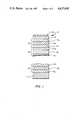
- FIG. 1is a fragmentary, cross-sectional view of a tandem photovoltaic device structured in accordance with the princples of the instant invention and comprising a plurality of n-i-p type photovoltaic cells;
- FIG. 2is a chart contrasting the photovoltaic properties of interest of the following narrow band gap precursor gaseous mixtures (1) SiH 4 , GeH 4 , H 2 ; (2) Si 2 H 6 , GeH 4 , H 2 ; (3) SiH 4 , GeH 4 , SiF 4 , H 2 ; and (4) Si 2 H 6 , GeH 4 , SiF 4 , H 2 .
- a photovoltaic cellformed of a plurality of successive n-i-p layers, each of which includes, preferably, an amorphous thin film semiconductor alloy material is shown generally by the reference numeral 10.
- FIG. 1shows an n-i-p type photovoltaic device such as a solar cell made up of individual n-i-p type cells 12a, 12b and 12c.
- a substrate 11which may be formed of a transparent glass or synthetic polymeric member; or formed from a metallic material such as stainless steel, aluminum, tantalum, molybdenum, chrome; or formed from metallic particles embedded within an insulator.
- a substrateshall include not only a flexible film, but also any elements added thereto by preliminary processing.
- Each of the cells 12a, 12b and 12care preferably fabricated with a thin film semiconductor body containing at least a silicon or silicon:germanium alloy.
- Each of the semiconductor bodiesincudes a p-type conductivity semiconductor layer 20a, 20b and 20c; a substantially intrinsic semiconductor layer 18a, 18b and 18c; and an n-type conductivity semiconductor layer 16a, 16b and 16c.
- the intrinsic layermay include traces of n-type or p-type dopant material without forfeiting its characteristic neutrality, hence it may be referred to herein as a "substantially intrinsic layer".
- cell 12bis an intermediate cell and, as indicated in FIG.
- n-i-p photovoltaic cellsare illustrated, the methods and materials of this invention may also be and are preferably utilized to produce single or multiple p-i-n cells. Accordingly, the term "n-i-p type" as used herein is meant to include any aggregation of n, i and p layers operatively disposed to provide a photoactive region for generating charge carriers in response to the absorption of photon energy. Additionally, semiconductor layers produced by instant invention may be readily employed to produce p-n cells, Schottky barrier cells, as well as other semiconductor devices such as diodes, memory arrays, photoconductive devices and the like.
- a further deposition processmay be either performed in a separate environment or as a part of a continuous process.
- a TCO (transparent conductive oxide) layer 22preferably formed of indium tin oxide, is added atop the p-layer 16c of the top most cell 12c.
- An electrode grid 24may be added to the device where the cell is of a sufficiently large area, or if the conductivity of the TCO layer 22 is insufficient to assume efficient collection of photogenerated current.
- the grid 24is adapted to shorten the carrier path and increase the conductive efficiency.
- the components of the mixtureare adapted to deposit high quality silicon based (approximately 1.7 eV band gap) semiconductor alloys.
- the process gas componentsinclude a silicon-containing gas, a fluorine-containing gas and a diluent-containing gas.
- the gaseous mixturewhen subjected to glow discharge deposition conditions, the parameters of which are detailed hereinbelow, readily deposits a high quality layer of silicon:fluorine:hydrogen material.
- a 5000 angstrom thick layer of said intrinsic silicon alloy material fabricated from this gaseous mixturemay be employed to fabricate a photovoltaic device having a fill factor of at least 0.7, an initial efficiency of at least 8.5%, and a resistance to photodegragation which quantitatively measures less than 10% after 20 hours of exposure to AM-1 illumination.
- the precursor gaseous mixtureincludes approximately 0.5 to 3.0 parts by volume of the silicon-containing gas which may be silane or a polyatomic silicon-containing species such as disilane or other higher order silanes.
- the fluorine-containing gasis present in approximately 0.01 to 3.0 parts by volume. As discussed previously, fluorine is believed to act, even in relatively small amounts, as a plasma organizer or calalyst and is thus deemed responsible for the high quality photoelectronic properties of the semiconductor alloy material deposited therefrom. A wide variety of fluorine-containing gas sources may be used.
- Silicon tetrafluoride gasis one fluorine-containing gas which has demonstrated particular utility, however elemental or molecular fluorine may also be advantageously employed as may be other fluorinated silicon compounds, fluorinated boron compounds, fluorinated phosphorous compounds, fluoro-carbons as well as combinations thereof.
- the fluorine-containing gasmay also form at least a portion of the silicon-containing gas, i.e. fluorinated silane and polysilane compounds may also be utilized.
- This class of precursor gaseous mixturesalso includes a diluent gas such as hydrogen, which gas (1) serves to control the rate of deposition of the depositing species, (2) serves to adjust the concentration of the depositing species to assure the optimum morphology of the deposit and (3) may also serve to facilitate the decomposition of the silicon-containing and/or fluorine- containing gases.
- a diluent gassuch as hydrogen
- gas (1)serves to control the rate of deposition of the depositing species
- (2)serves to adjust the concentration of the depositing species to assure the optimum morphology of the deposit
- (3)may also serve to facilitate the decomposition of the silicon-containing and/or fluorine- containing gases.
- hydrogenis one prefered diluent gas
- other gasessuch as nitrogen or inert gases such as helium, argon, neon and xenon may be similarly employed.
- These precursor gaseous mixturesmay comprise, for example, by volume approximately 0.5 to 3.0 parts of the silicon-containing gas, 0.01 to 3.0
- Dopant gasesmay also be included in the deposition mixture to provide for the glow discharge deposition of doped layers of semiconductor alloy material.
- Typical dopant gasessuch as, for example phosphine, diborane, phosphorous trifluoride, phosphorous pentafluoride, and boron trifluoride may also be employed. It should be noted that the latter three dopant gases, since they include fluorine, may also function as the source of fluorine for the precursor gaseous mixture.
- the previously described precursor gaseous mixturesmay include a germanium-containing gas therein in addition to the silicon-containing gas, fluorine-containing gas and diluent gas.
- a germanium-containing gastherein in addition to the silicon-containing gas, fluorine-containing gas and diluent gas.
- Such a mixturemay be employed to deposit a narrow band gap layer of semiconductor alloy material having at least 20% germanium incorporated into the host matrix thereof.
- Said narrow band gap semiconductor alloy materialwhen utilized as the intrinsic layer of a single cell photovoltaic device, provides a photoconversion efficiency of greater than 6.5%.
- the silicon-containing, fluorine-containing and diluent gasesmay be as previously described, while the germanium-containing gas may be chosen from readily available germanium-containing gaseous compounds.
- germane gasis preferred, germanium tetrafluoride and other fluorinated germanium-containing compounds may also be employed with advantage and may, in some cases, also serve as the source of fluorine in the precursor mixture.
- the germanium-containing gasis preferably introduced so as to be present in the mixture in the same range as the silicon-containing gas, that is to say from 0.5 to 3.0 parts by volume.
- Another class of precursor gaseous mixtures of the instant inventionincludes a polyatomic silicon-containing gas such as disilane or other higher order silanes as well as variously substituted analogues thereof, in conjunction with a germanium-containing gas such as germane.
- the two semiconductor-containing gasesmust be chosen to decompose and deposit their respective semiconductor species at approximately equal rates when subjected to the electromagnetic field of a glow discharge deposition system. In this manner, the components of the mixture serve to substantially eliminate heretofore encountered gas depletion problems.
- the silicon-containing componentis disilane and the germanium-containing component is germane.
- Other silicon-containing gasessuch as trisilane or other higher order silanes may also be advantageously employed.
- the precursor gaseous mixturealso typically includes a diluent gas such as hydrogen or an inert gas, as previously enumerated, to control the rate of deposition, to adjust the concentration of the semiconductor-containing gases for assuring optimum morphology and, in some cases, to assist in the decomposition of the precursor gaseous mixture.
- a diluent gassuch as hydrogen or an inert gas, as previously enumerated, to control the rate of deposition, to adjust the concentration of the semiconductor-containing gases for assuring optimum morphology and, in some cases, to assist in the decomposition of the precursor gaseous mixture.
- the nondepleting precursor gaseous mixture for depositing the narrow band gap semiconductor alloy materialmay be utilized as described, it has been found that the inclusion of even small amounts of a fluorine-containing gas therein will organize plasma conditions and assure the deposition of desired species from the plasma.
- Fluorinemay be provided from any of the previously discussed gaseous sources.
- the precursor gaseous mixtureswill include 0.3 to 3.0 parts by volume of the polyatomic silicon-containing gas, 0.3 to 3.0 parts by volume of the germanium-containing gas and 3 to 30 parts by volume of the diluent gas. If fluroine is included, the fluorine-containing gas is present in 0.01 to 3.0 parts by volume.
- the mixturemay also include a dopant gas therein, which dopant may also serve as the source of fluorine.
- the glow discharge deposition of semiconductor alloy materialis carried out within the vacuum envelope of a deposition chamber in order to isolate the deposition atmosphere from ambient conditions and provide the type of low pressure regime needed for igniting and sustaining the plasma and limiting unwanted molecular and atomic collisions.
- the deposition chamberis typically formed of a nonpermeable material such as glass or metal and has one or more vacuum pumps connected thereto for the evacuation of the atmosphere therefrom.
- the deposition chamberalso includes one or more gas introduction manifolds for introducing any combination of the discrete process gases, which combine to form the precursor gaseous mixture, into the chamber.
- a supportfor maintaining the a substrate a fixed distance from the cathode for the uniform deposition of semiconductor alloy material thereonto.
- the source of electromagnetic energymay include a cathode or an antenna depending on the type of electromagnetic energy employed.
- the precursor gaseous mixtures of the instant inventionmay be employed, with equal effectiveness, in microwave or radio frequency energized systems. Radio frequency excitation of the precursor gaseous mixture is typically accomplished by introducing the mixture into the plasma region formed between the generally planar cathode plate and the substrate which, as stated above, is disposed in relatively close proximity thereto.
- microwavesare generally introduced either from an antenna designed to radiate microwave energy into the deposition chamber, or in other embodiements, from a source such as a magnetron coupled to a waveguide cavity.
- a sourcesuch as a magnetron coupled to a waveguide cavity.
- the substratepreferably forms at least a portion of the waveguide cavity and the precursor gaseous mixture is introduced adjacent thereto so that the deposition occurs directly onto the substrate.
- the glow discharge deposition of semiconductor alloy materialmay be carried out in either a batch or continuous mode of production.
- a batch deposition processa single chamber is generally employed for the deposition of the material onto a discrete substrate which is loaded thereinto.
- Continuous processingis most advantageously employed for the high volume deposition of the semiconductor alloy material, and hence the mass production of photovoltaic devices therefrom.
- a plurality of interconnected and vacuumized deposition chambersare provided. Each chamber is interconnected to adjacent chambers by discrete isolation chambers which allow for the continuous passage of an elongated web of substrate material therebetween while preventing the gaseous environments of the adjacent chambers from contaminating one another.
- a single elongated web of substrate materialmay be continuously advanced through the plurality of deposition chambers for the depositon of successive layers of doped or intrinsic semiconductor alloy material thereonto.
- the precursor gaseous mixtures of the instant inventionmay be advantageously employed in either the batch or in the continuous modes of production; however, it is in the high volume, continuous deposition of semiconductor alloy material onto a web of substrate material that the aforementioned problems of gas depletion are the most significant.
- the deposition chamber or chambers employedit is the decomposition of the precursor gaseous mixture which results in the formation of the semiconductor deposit.
- the electromagnetic energyacts upon the precursor gaseous mixture to generate a host of activated species therefrom by a process that may include ionizing, radicalizing, or otherwise activating the molecules of the mixture gas to form the highly energetic species. While it is desirable to limit the number of molecular collisions within the uncontrolled environment of the plasma, these activated deposition species interact (collide) with one another until they are finally deposited onto the substrate.
- the number of collisions, the composition of the colliding molecules, the form and number of ions and free radicalsmay be controlled to some extent by varying systems parameters such as the pressure within the chamber, the temperature of the substrate, the external bias placed upon the substrate, as well as, of course, the relative ratio and nature of the components of the precursor gaseous mixture.
- a substrateis first moved into the deposition chamber, the substrate is heated to the deposition temperature, typically 150°-3000°, the chamber evacuated to the working pressure range, typically a range of about 0.5 to 10 torr and the components of the precursor gaseous mixture are introduced thereinto so as to create a gaseous atmosphere at least in the region proximate the substrate.
- Electromagnetic energyis then provided, either by a electrode or an antenna as described previously, to effect the decomposition of the precursor gaseous mixture and the deposition of the semiconductor alloy material.
- the sampleswere prepared by the radio frequency energized glow discharge deposition of five precursor gaseous mixtures differing from one another only in the amount of the silicon tetrafluoride gas component included therein.
- the quality of the thus deposited alloyswas assessed by measuring the photoconductivity thereof in the coplanar direction by techniques well known to those skilled in the art.
- photoconductivityitself cannot be regarded as a full and total measure of the photovoltaic quality of a particular layer of semiconductor alloy material insofar as the photoconductivity depends, inter alia, upon the activation energy of that alloy material.
- no significant differences in activation energy between any of the sampleswas seen. Accordingly, the measured photoconductivity of the material provided a good indication of the actual photovoltaic quality of the particular samples.
- the first sampleincluded no silicon tetrafluoride in the precursor gaseous mixture thereof and resulted in the deposition of semiconductor alloy material having the lowest photoconductivity, i.e., (1) X 10 -5 inverse ohms-centimeters.
- the second sample5 sccm of silicon tetrafluoride was introduced into the deposition chamber, which flow rate resulted in the deposition of a semiconductor alloy material having a photoconductivity three to four times higher than that of the non-fluorinated sample.
- disilane and germanedecompose and deposit semiconductor alloy material at a rate greater than the rate of deposition of semiconductor alloy material deposited from silicon tetrafluoride.
- fluorineexerts a very significant effect in the deposition of high quality photovoltaic alloy films and this effect is manifested even when fluorine is introduced into the precursor gaseous mixture, for plasma deposition, in exceedingly small amounts. It can therefore be hypothesized that fluorine acts catalytically to organize the tetrahedral coordination of depositing species, and/or to remove weakly bond atoms and molecules from the depositing layer of semiconductor alloy material and/or to passivate dangling or vacant bonds for assuring the deposition of only high quality semiconductor alloy materials.
- n-i-p type photovoltaic cellwhich cell included a 1500 angstrom thick intrinsic layer, said layer deposited from a precursor gaseous mixture of 2% Si 2 H 6 , 96% H 2 and 2% SiF 4 .
- the intrinsic layerwas sandwiched between n and p doped silicon alloy layers of approximately 150 angstroms thickness. All layers were deposited by the 13.56 MHz radio frequency energized glow discharge decomposition technique previously described.
- the efficiency of the thus produced photovoltaic devicewas approximately 6.2% as measured under AM-1 illumination.
- the open circuit voltage of that devicewas 9.24 volts and the fill factor was 0.730.
- a similarly prepared photovoltaic cell having an approximately 2000 angstrom thick intrinsic layer and exhibiting an initial efficiency of approximately 8.4%was exposed to AM-1 illumination to assess the photodegradation thereof. It was found that after 75 hours of illumination, a loss of only 5% of the initial operating efficiency occurred. This level of photodegradation is to be compared with a typical loss in photoconversion efficiency exceeding 25% for similarly configured photovoltaic cells fabricated from silane and hydrogen but specifically excluding fluorine.
- Photoconductivity of the sample deposited from the disilane-fluorine mixturewas 3 ⁇ 10 -5 inverse ohms-centimeters whereas the photoconductivity of the disilane and the fluorinated silane prepared samples was only 1 ⁇ 10 -5 inverse ohms-centimeter. Furthermore, the sub-band gap absorption of the latter two samples was approximately 3-4 times higher than for the sample prepared from the disilane-fluorine mixture.
- An analysis of the deposited filmshowed that approximately 10-15% hydrogen was present in all three samples whereas fluorine was present in the disilane-fluorine prepared sample and the silane-fluorine prepared sample at no more than 0.1%. Additionally, it was found that the sample prepared from the disilane-fluorine mixture included approximately 40% germanium, the largest reported amount of germanium that has been included in a silicon alloy film without detrimentally affecting the electronic properties thereof.
- FIG. 2there is illustrated a table summarizing data derived from an experimental series assessing the effect of the precursor gaseous mixtures of the instant invention on the preparation of silicon:germanium alloys. It will be noted from an inspection of that Figure that four separate categories of precursor gaseous mixtures were used to deposit different films of semiconductor alloy material.
- the first column of the table in FIG. 2represents semiconductor alloys prepared from a precursor gaseous mixture comprising silane, germane, hydrogen and in some cases, trace amounts of diborane.
- the second columnrepresents semiconductor alloys prepared from a precursor gaseous mixture comprising disilane, germane and hydrogen.
- the third columnrepresents alloys prepared from a precursor gaseous mixture comprising silane, germane, silicon tetrafluoride and hydrogen with the inclusion of, in some cases, trace amounts of diborane.
- the fourth columnrepresents alloys prepared from a precursor gaseous mixture of disilane, germane, silicon tetrafluoride and hydrogen.
- the first group of sampleswas prepared from a precursor gaseous mixture comprising 10 sccm of hydrogen, 1 sccm of germane, 8 sccm of silane and 3 sccm of a mixture of 500 ppm of diborane in hydrogen (where used).
- the second group of sampleswere prepared from a precursor gaseous mixture comprising 32 sccm of hydrogen, 2 sccm of germane, and 2.5 sccm of disilane.
- the third group of sampleswere prepared from a precursor gaseous mixture comprising 4 sccm of hydrogen, 7 sccm of silicon tetrafluoride, 1 sccm of germane, 7 sccm of silane and 3 sccm of a mixture of 500 ppm of diborane in hydrogen (where used).
- the fourth group of sampleswere prepared from a precursor gaseous mixture comprising 52 sccm of hydrogen, 2.5 sccm of silicon tetrafluoride, 2.0 sccm of germane, and 2.5 sccm of disilane. It should be noted, as previously discussed, all rates are nominal.
- the photoconductivity of the silicon:germanium:fluorine:hydrogen alloy deposited from the mixture including disilane and fluorineis approximately 2-3 ⁇ 10 -5 inverse ohms-centimeters, which photoconductivity is at least one order of magnitude higher than the photoconductivity of 3-6 ⁇ 10 -6 inverse ohms-centimeters manifested by the other three samples.
- the inclusion of small amounts of boron into the deposited semiconductor alloy materialeffects an increase in the photoconductivity, although as will be explained below, this increase is not reflected in improved electronic properties.
- the dark conductivity of all four of the layers of semiconductor alloy materialis fairly high, i.e., in the range of 10 -8 -10 -9 inverse ohms-centimeters, a figure in the "noise" level of measurment for purposes of this comparison.
- the band gaps of the four groups of semiconductor alloy samplesare all approximately 1.5 eV, indicating that relatively similar amounts of germanium were incorporated into the host matrix of each.
- the activation energy of the four groups of samplesare relatively similar, although it will be noted that the two groups of samples deposited from the disilane-containing gas have a slightly lower activation energy than do the silane deposited samples. This shift in Fermi level position is very slight and is comparable to the shift produced by trace amounts of the boron dopant. In any case, the shift in the Fermi level is of a sufficiently small magnitude that all of the the samples may be regarded as being of substantially intrinsic conductivity type.
- Tail statesare those defect states (such as dangling bonds, strained bonds, vacant bonds, etc.) which occur at the edge of the band gap.
- a high density of tail stateswill impede charge carriers travelling across the band gap by providing traps and other recombination centers.
- any semiconductor alloy materialit is desirable to have the total density of states as low as possible in order to promote a maximum number of charge carriers to the conduction band and to secure optimum electrical properties therefrom.
- the sub-band gap absorptions of the sampleswere measured by photodeflection spectroscopy at an energy of 1.1 eV and thus are indicative of states proximate the edge of the valence band.
- the relative density of tail states of the samples prepared from the fluorinated and nonfluorinated silane mixtures, as well as the nonfluorinated disilane prepared samplesis 5 to 10 times higher than that of the samples prepared from disilane and fluorine.
- the addition of trace amounts of boronhas no effect whatsoever upon the density of tail states. It should be clear from this data that there is a synergistic effect occurring with the combination of a fluorine-containing gas and disilane, which effect reduces the density of tail states in a manner which neither disilane or fluorine can accomplish individually.
- Representative samples of the various layers of semiconductor alloy material represented hereinwere fabricated into single n-i-p-type photovoltaic cells. This was accomplished by well known techniques in which a layer of n-type silicon alloy material was first deposited upon an electrically conductive stainless steel substrate. The n-type alloy in each case was a microcrystalline n-type layer of approximately 150 angstrom thickness. Atop this n-type layer, an approximately 2000 angstrom thick layer of substantially intrinsic semiconductor alloy material was deposited, followed by the deposition thereupon of a layer of microcrystalline p-type silicon alloy material of approximately 150 angstrom thickness.
- the photovoltaic devicewas completed by depositing a transparent, electrically conductive top electrode of approximately 450 angstroms of indium tin oxide atop the p-type layer. In this manner, the two doped layers cooperate to provide an electric field across the intrinsic layer for generating a photoactive region therein, in which region the absorption of photons from incident radiation generates charge carriers which are subsequently collected at the substrate electrode and the indium tin oxide electrode.
- Photodegradationalso termed Staebler-Wronski degradation
- Staebler-Wronski degradationis one of the biggest problems which has heretofore plagued prior art amorphous photovoltaic devices.
- This degradationalthough poorly understood, is a light induced process which derogatorily affects the efficiency of photovoltaic devices. It has been found that photodegradation proceeds in an exponential manner with initial degradation being very rapid and quickly reaching a saturation limit.
- silane based silicon:germanium alloy samples not containing boronhad a high density of defect states as initially prepared and, accordingly, photodegradation could not be readily measured in the photovoltaic devices in which they were incorporated.
- the inclusion of small amounts of boron in those alloy sampleswas necessary in order to produce a photovoltaic device having sufficient operational efficiency to allow for measurement of photodegradation.
- the disilane, germane hydrogen material, as preparedwas also a fairly high defect material which could not be readily fabricated into a useable photovoltaic cell; accordingly no data can be presented for photodegradation of these samples.
- the nonfluorinated silicon:germanium alloy cellexhibited the highest photodegradation, i.e.,. a loss in efficiency of 34% after only 16 hours of AM-1 illumination.
- Incorporation of fluorine into the precursor gaseous mixture thereofeffected a significant reduction in the photodegradation, resulting in a cell which degraded only 12% after that 16 hours of exposure.
- Photovoltaic cells produced from an alloy deposited from that mixtureexhibited only a 5% degradation after 16 hours of exposure.
- disilaneincreases the deposition rate of silicon-containing germanium alloys
- fluorineto silicon:germanium alloys improves the stability and efficiency of those alloys
- the combination of disilane and fluorineprovides a high deposition rate and interacts synergistically to form a semiconductor alloy exhibiting greatly increased resistance to photodegradation, a lower density of defect states in the band gap thereof and increased photovoltaic efficiency.
Landscapes
- Engineering & Computer Science (AREA)
- Physics & Mathematics (AREA)
- Condensed Matter Physics & Semiconductors (AREA)
- General Physics & Mathematics (AREA)
- Manufacturing & Machinery (AREA)
- Computer Hardware Design (AREA)
- Microelectronics & Electronic Packaging (AREA)
- Power Engineering (AREA)
- Chemical & Material Sciences (AREA)
- Materials Engineering (AREA)
- Photovoltaic Devices (AREA)
Abstract
Description
TABLE 1______________________________________Flow Rates (SCCM)Sample Si.sub.2 H.sub.6 SiF.sub.4 GeH.sub.4 H.sub.2 ph (ohm-cm).sup.-1______________________________________I. 5 0 5 50 1 × 10.sup.-5II. 5 5 5 50 3-4 × 10.sup.-5III. 5 2.5 5 50 3-4 × 10.sup.-5IV. 5 1.25 5 50 3-4 × 10.sup.-5V. 5 .6 5 50 2 × 10.sup.-5______________________________________
Claims (9)
Priority Applications (11)
| Application Number | Priority Date | Filing Date | Title |
|---|---|---|---|
| US06/718,661US4637895A (en) | 1985-04-01 | 1985-04-01 | Gas mixtures for the vapor deposition of semiconductor material |
| DE8686301938TDE3681074D1 (en) | 1985-04-01 | 1986-03-17 | GAS MIXTURES AND METHOD FOR DEPOSIT OF AMORPHOUS SEMICONDUCTORS. |
| EP86301938AEP0204396B1 (en) | 1985-04-01 | 1986-03-17 | Gas mixtures and processes for deposition of amorphous semiconductors |
| ES553394AES8705929A1 (en) | 1985-04-01 | 1986-03-25 | Gas mixtures and processes for deposition of amorphous semiconductors. |
| ZA862255AZA862255B (en) | 1985-04-01 | 1986-03-26 | Gas mixtures and process for deposition of amorphous semiconductors |
| BR8601421ABR8601421A (en) | 1985-04-01 | 1986-03-31 | GAS PRECURSOR MIXTURE AND MANUFACTURING PROCESS OF A SEMICONDUCTOR ALLOY |
| MX002030AMX166176B (en) | 1985-04-01 | 1986-03-31 | GAS MIXTURES AND PROCEDURE FOR THE DEPOSIT OF AMORPHOUS SEMICONDUCTORS |
| JP61074116AJPH07123113B2 (en) | 1985-04-01 | 1986-03-31 | Method for manufacturing pin type photovoltaic cell |
| AU55531/86AAU576147B2 (en) | 1985-04-01 | 1986-04-01 | Gas mixtures for deposition of amorphous semiconductors |
| US06/897,236US4696758A (en) | 1985-04-01 | 1986-10-06 | Gas mixtures for the vapor deposition of semiconductor material |
| US06/897,449US4698234A (en) | 1985-04-01 | 1986-10-17 | Vapor deposition of semiconductor material |
Applications Claiming Priority (1)
| Application Number | Priority Date | Filing Date | Title |
|---|---|---|---|
| US06/718,661US4637895A (en) | 1985-04-01 | 1985-04-01 | Gas mixtures for the vapor deposition of semiconductor material |
Related Child Applications (2)
| Application Number | Title | Priority Date | Filing Date |
|---|---|---|---|
| US06/897,236ContinuationUS4696758A (en) | 1985-04-01 | 1986-10-06 | Gas mixtures for the vapor deposition of semiconductor material |
| US06/897,449DivisionUS4698234A (en) | 1985-04-01 | 1986-10-17 | Vapor deposition of semiconductor material |
Publications (1)
| Publication Number | Publication Date |
|---|---|
| US4637895Atrue US4637895A (en) | 1987-01-20 |
Family
ID=24886972
Family Applications (3)
| Application Number | Title | Priority Date | Filing Date |
|---|---|---|---|
| US06/718,661Expired - LifetimeUS4637895A (en) | 1985-04-01 | 1985-04-01 | Gas mixtures for the vapor deposition of semiconductor material |
| US06/897,236Expired - LifetimeUS4696758A (en) | 1985-04-01 | 1986-10-06 | Gas mixtures for the vapor deposition of semiconductor material |
| US06/897,449Expired - LifetimeUS4698234A (en) | 1985-04-01 | 1986-10-17 | Vapor deposition of semiconductor material |
Family Applications After (2)
| Application Number | Title | Priority Date | Filing Date |
|---|---|---|---|
| US06/897,236Expired - LifetimeUS4696758A (en) | 1985-04-01 | 1986-10-06 | Gas mixtures for the vapor deposition of semiconductor material |
| US06/897,449Expired - LifetimeUS4698234A (en) | 1985-04-01 | 1986-10-17 | Vapor deposition of semiconductor material |
Country Status (9)
| Country | Link |
|---|---|
| US (3) | US4637895A (en) |
| EP (1) | EP0204396B1 (en) |
| JP (1) | JPH07123113B2 (en) |
| AU (1) | AU576147B2 (en) |
| BR (1) | BR8601421A (en) |
| DE (1) | DE3681074D1 (en) |
| ES (1) | ES8705929A1 (en) |
| MX (1) | MX166176B (en) |
| ZA (1) | ZA862255B (en) |
Cited By (88)
| Publication number | Priority date | Publication date | Assignee | Title |
|---|---|---|---|---|
| US4801474A (en)* | 1986-01-14 | 1989-01-31 | Canon Kabushiki Kaisha | Method for forming thin film multi-layer structure member |
| US4824697A (en)* | 1986-01-14 | 1989-04-25 | Canon Kabushiki Kaisha | Method for forming a multi-layer deposited film |
| US4826711A (en)* | 1985-08-08 | 1989-05-02 | Semiconductor Energy Laboratory Co., Ltd. | Semiconductor manufacturing method and device |
| US4868014A (en)* | 1986-01-14 | 1989-09-19 | Canon Kabushiki Kaisha | Method for forming thin film multi-layer structure member |
| US4891330A (en)* | 1987-07-27 | 1990-01-02 | Energy Conversion Devices, Inc. | Method of fabricating n-type and p-type microcrystalline semiconductor alloy material including band gap widening elements |
| US5016985A (en)* | 1988-06-24 | 1991-05-21 | Kaiser Aerospace & Electronics Corporation | Infrared filter using cholesteric liquids |
| US5089872A (en)* | 1990-04-27 | 1992-02-18 | North Carolina State University | Selective germanium deposition on silicon and resulting structures |
| US5101247A (en)* | 1990-04-27 | 1992-03-31 | North Carolina State University | Germanium silicon dioxide gate MOSFET |
| US5591492A (en)* | 1986-04-11 | 1997-01-07 | Canon Kabushiki Kaisha | Process for forming and etching a film to effect specific crystal growth from activated species |
| US20020116955A1 (en)* | 2001-02-19 | 2002-08-29 | Sumitomo Electric Industries, Ltd. | Method of forming soot preform |
| US20020168852A1 (en)* | 2001-05-11 | 2002-11-14 | Harshfield Steven T. | PCRAM memory cell and method of making same |
| US20030027416A1 (en)* | 2001-08-01 | 2003-02-06 | Moore John T. | Method of forming integrated circuitry, method of forming memory circuitry, and method of forming random access memory circuitry |
| US20030045049A1 (en)* | 2001-08-29 | 2003-03-06 | Campbell Kristy A. | Method of forming chalcogenide comprising devices |
| US20030047772A1 (en)* | 2001-03-15 | 2003-03-13 | Jiutao Li | Agglomeration elimination for metal sputter deposition of chalcogenides |
| US20030096497A1 (en)* | 2001-11-19 | 2003-05-22 | Micron Technology, Inc. | Electrode structure for use in an integrated circuit |
| US20030117831A1 (en)* | 2001-12-20 | 2003-06-26 | Glen Hush | Programmable conductor random access memory and a method for writing thereto |
| US20030128612A1 (en)* | 2002-01-04 | 2003-07-10 | John Moore | PCRAM rewrite prevention |
| US20030156468A1 (en)* | 2002-02-20 | 2003-08-21 | Campbell Kristy A. | Resistance variable 'on' memory |
| US20030155606A1 (en)* | 2002-02-15 | 2003-08-21 | Campbell Kristy A. | Method to alter chalcogenide glass for improved switching characteristics |
| US20030156463A1 (en)* | 2002-02-19 | 2003-08-21 | Casper Stephen L. | Programmable conductor random access memory and method for sensing same |
| US20030169625A1 (en)* | 2002-03-05 | 2003-09-11 | Glen Hush | Programmable conductor random access memory and method for sensing same |
| US20030173558A1 (en)* | 2002-03-14 | 2003-09-18 | Campbell Kristy A. | Methods and apparatus for resistance variable material cells |
| US20030193053A1 (en)* | 2002-04-10 | 2003-10-16 | Gilton Terry L. | Thin film diode integrated with chalcogenide memory cell |
| US20030194865A1 (en)* | 2002-04-10 | 2003-10-16 | Gilton Terry L. | Method of manufacture of programmable conductor memory |
| US20030193059A1 (en)* | 2002-04-10 | 2003-10-16 | Gilton Terry L. | Programmable conductor memory cell structure and method therefor |
| US20040007718A1 (en)* | 2001-08-30 | 2004-01-15 | Campbell Kristy A. | Stoichiometry for chalcogenide glasses useful for memory devices and method of formation |
| US20040007749A1 (en)* | 2002-07-10 | 2004-01-15 | Campbell Kristy A. | Assemblies displaying differential negative resistance |
| US20040029351A1 (en)* | 2002-01-31 | 2004-02-12 | Gilton Terry L. | Methods of forming non-volatile resistance variable devices and methods of forming silver selenide comprising structures |
| US20040038480A1 (en)* | 2002-08-22 | 2004-02-26 | Moore John T. | Method of manufacture of a PCRAM memory cell |
| US20040040837A1 (en)* | 2002-08-29 | 2004-03-04 | Mcteer Allen | Method of forming chalcogenide sputter target |
| US20040040835A1 (en)* | 2002-08-29 | 2004-03-04 | Jiutao Li | Silver selenide film stoichiometry and morphology control in sputter deposition |
| US20040043553A1 (en)* | 2002-06-06 | 2004-03-04 | Jiutao Li | Elimination of dendrite formation during metal/chalcogenide glass deposition |
| US20040043245A1 (en)* | 2002-08-29 | 2004-03-04 | Moore John T. | Method to control silver concentration in a resistance variable memory element |
| US20040053461A1 (en)* | 2002-08-29 | 2004-03-18 | Moore John T. | Graded GexSe100-x concentration in PCRAM |
| US20040124406A1 (en)* | 2001-08-29 | 2004-07-01 | Campbell Kristy A. | Method of forming non-volatile resistance variable devices, method of forming a programmable memory cell of memory circuitry, and a non-volatile resistance variable device |
| US20040130598A1 (en)* | 2002-07-10 | 2004-07-08 | Canon Kabushiki Kaisha | Ink jet record head |
| US20040157417A1 (en)* | 2002-08-29 | 2004-08-12 | Moore John T. | Methods to form a memory cell with metal-rich metal chalcogenide |
| US20040161874A1 (en)* | 2001-03-01 | 2004-08-19 | Moore John T. | Method of forming a non-volatile resistance variable device, and non-volatile resistance variable device |
| US20040175859A1 (en)* | 2002-08-29 | 2004-09-09 | Campbell Kristy A. | Single polarity programming of a PCRAM structure |
| US20040180533A1 (en)* | 2003-03-14 | 2004-09-16 | Li Li | Method for filling via with metal |
| US20040192006A1 (en)* | 2002-02-20 | 2004-09-30 | Campbell Kristy A. | Layered resistance variable memory device and method of fabrication |
| US20040202016A1 (en)* | 2003-04-10 | 2004-10-14 | Campbell Kristy A. | Differential negative resistance memory |
| US6809362B2 (en) | 2002-02-20 | 2004-10-26 | Micron Technology, Inc. | Multiple data state memory cell |
| US20040211957A1 (en)* | 2002-08-29 | 2004-10-28 | Moore John T. | Method and apparatus for controlling metal doping of a chalcogenide memory element |
| US6813178B2 (en) | 2003-03-12 | 2004-11-02 | Micron Technology, Inc. | Chalcogenide glass constant current device, and its method of fabrication and operation |
| US20040235235A1 (en)* | 2002-06-06 | 2004-11-25 | Jiutao Li | Co-sputter deposition of metal-doped chalcogenides |
| US6833559B2 (en) | 2001-02-08 | 2004-12-21 | Micron Technology, Inc. | Non-volatile resistance variable device |
| US20040264234A1 (en)* | 2003-06-25 | 2004-12-30 | Moore John T. | PCRAM cell operation method to control on/off resistance variation |
| US20050018509A1 (en)* | 2001-11-20 | 2005-01-27 | Glen Hush | Complementary bit resistance memory sensor and method of operation |
| US20050017233A1 (en)* | 2003-07-21 | 2005-01-27 | Campbell Kristy A. | Performance PCRAM cell |
| US20050026433A1 (en)* | 2001-08-30 | 2005-02-03 | Jiutao Li | Integrated circuit device and fabrication using metal-doped chalcogenide materials |
| US20050054207A1 (en)* | 2002-08-29 | 2005-03-10 | Micron Technology, Inc. | Plasma etching methods and methods of forming memory devices comprising a chalcogenide comprising layer received operably proximate conductive electrodes |
| US20050056910A1 (en)* | 2003-09-17 | 2005-03-17 | Gilton Terry L. | Non-volatile memory structure |
| US6894304B2 (en) | 2001-08-27 | 2005-05-17 | Micron Technology, Inc. | Apparatus and method for dual cell common electrode PCRAM memory device |
| US20050162907A1 (en)* | 2004-01-28 | 2005-07-28 | Campbell Kristy A. | Resistance variable memory elements based on polarized silver-selenide network growth |
| US20050162883A1 (en)* | 2002-08-08 | 2005-07-28 | Hasan Nejad | Columnar 1T-nMemory cell structure and its method of formation and operation |
| US20050167689A1 (en)* | 2004-01-29 | 2005-08-04 | Campbell Kristy A. | Non-volatile zero field splitting resonance memory |
| US20050202588A1 (en)* | 2004-03-10 | 2005-09-15 | Brooks Joseph F. | Method of forming a chalcogenide material containing device |
| US20050201174A1 (en)* | 2004-03-10 | 2005-09-15 | Klein Dean A. | Power management control and controlling memory refresh operations |
| US6961277B2 (en) | 2003-07-08 | 2005-11-01 | Micron Technology, Inc. | Method of refreshing a PCRAM memory device |
| US20060011910A1 (en)* | 2004-07-19 | 2006-01-19 | Micron Technology, Inc. | PCRAM device with switching glass layer |
| US20060012008A1 (en)* | 2004-07-19 | 2006-01-19 | Campbell Kristy A | Resistance variable memory device and method of fabrication |
| US20060033094A1 (en)* | 2004-08-12 | 2006-02-16 | Campbell Kristy A | Resistance variable memory with temperature tolerant materials |
| US20060035403A1 (en)* | 2004-08-12 | 2006-02-16 | Campbell Kristy A | PCRAM device with switching glass layer |
| US20060044906A1 (en)* | 2004-09-01 | 2006-03-02 | Ethan Williford | Sensing of resistance variable memory devices |
| US7010644B2 (en) | 2002-08-29 | 2006-03-07 | Micron Technology, Inc. | Software refreshed memory device and method |
| US20060131556A1 (en)* | 2004-12-22 | 2006-06-22 | Micron Technology, Inc. | Small electrode for resistance variable devices |
| US20060131555A1 (en)* | 2004-12-22 | 2006-06-22 | Micron Technology, Inc. | Resistance variable devices with controllable channels |
| US20060237707A1 (en)* | 2005-04-22 | 2006-10-26 | Micron Technology, Inc. | Memory array for increased bit density and method of forming the same |
| US20060256640A1 (en)* | 2005-05-16 | 2006-11-16 | Micron Technology, Inc. | Power circuits for reducing a number of power supply voltage taps required for sensing a resistive memory |
| US20060270099A1 (en)* | 2001-08-29 | 2006-11-30 | Micron Technology, Inc. | Method of forming non-volatile resistance variable devices and method of forming a programmable memory cell of memory circuitry |
| US20070008768A1 (en)* | 2005-07-08 | 2007-01-11 | Micron Technology, Inc. | Process for erasing chalcogenide variable resistance memory bits |
| US20070007506A1 (en)* | 2002-02-20 | 2007-01-11 | Micron Technology, Inc. | Layered resistance variable memory device and method of fabrication |
| US20070023744A1 (en)* | 2005-08-01 | 2007-02-01 | Micron Technology, Inc. | Resistance variable memory device with sputtered metal-chalcogenide region and method of fabrication |
| US20070029537A1 (en)* | 2005-08-02 | 2007-02-08 | Micron Technology, Inc. | Phase change memory cell and method of formation |
| US20070030554A1 (en)* | 2005-08-02 | 2007-02-08 | Micron Technology, Inc. | Method and apparatus for providing color changing thin film material |
| US20070037316A1 (en)* | 2005-08-09 | 2007-02-15 | Micron Technology, Inc. | Memory cell contact using spacers |
| US20070034921A1 (en)* | 2005-08-09 | 2007-02-15 | Micron Technology, Inc. | Access transistor for memory device |
| US20070035990A1 (en)* | 2005-08-15 | 2007-02-15 | Micron Technology, Inc. | Method and apparatus providing a cross-point memory array using a variable resistance memory cell and capacitance |
| US20070047297A1 (en)* | 2005-08-31 | 2007-03-01 | Campbell Kristy A | Resistance variable memory element with threshold device and method of forming the same |
| US20070059882A1 (en)* | 2005-04-22 | 2007-03-15 | Micron Technology, Inc. | Memory elements having patterned electrodes and method of forming the same |
| US20070090354A1 (en)* | 2005-08-11 | 2007-04-26 | Micron Technology, Inc. | Chalcogenide-based electrokinetic memory element and method of forming the same |
| US7269044B2 (en) | 2005-04-22 | 2007-09-11 | Micron Technology, Inc. | Method and apparatus for accessing a memory array |
| US7294527B2 (en) | 2002-08-29 | 2007-11-13 | Micron Technology Inc. | Method of forming a memory cell |
| US7317200B2 (en) | 2005-02-23 | 2008-01-08 | Micron Technology, Inc. | SnSe-based limited reprogrammable cell |
| US20090261316A1 (en)* | 2006-08-29 | 2009-10-22 | Jun Liu | Enhanced memory density resistance variable memory cells, arrays, devices and systems including the same, and methods of fabrication |
| US20110037558A1 (en)* | 2008-08-01 | 2011-02-17 | Boise State University | Continuously variable resistor |
| US20220020583A1 (en)* | 2020-07-19 | 2022-01-20 | Applied Materials, Inc. | Hydrogen management in plasma deposited films |
Families Citing this family (35)
| Publication number | Priority date | Publication date | Assignee | Title |
|---|---|---|---|---|
| JPH0624238B2 (en)* | 1985-04-16 | 1994-03-30 | キヤノン株式会社 | Photosensor array manufacturing method |
| JPH0637703B2 (en)* | 1986-12-22 | 1994-05-18 | 三井東圧化学株式会社 | Semiconductor thin film manufacturing method |
| US5041303A (en)* | 1988-03-07 | 1991-08-20 | Polyplasma Incorporated | Process for modifying large polymeric surfaces |
| US4961829A (en)* | 1988-09-30 | 1990-10-09 | Semi-Conductor Devices, A Tadiran-Rafael Partnership | Passivation of semiconductor surfaces |
| JPH0298128A (en)* | 1988-10-04 | 1990-04-10 | Agency Of Ind Science & Technol | Formation of semiconductor thin film |
| IT1227877B (en)* | 1988-11-25 | 1991-05-14 | Eniricerche S P A Agip S P A | PROCEDURE FOR PLASMA DEPOSITION OF MULTIPLE LAYERS SIZED AMORPHOUS VARIABLE COMPOSITION |
| JP2693032B2 (en)* | 1990-10-16 | 1997-12-17 | キヤノン株式会社 | Method for forming semiconductor layer and method for manufacturing solar cell using the same |
| US5482656A (en)* | 1993-03-04 | 1996-01-09 | Kabushiki Kaisha Toshiba | Non-linear optical devices employing a polysilane composition and a polysilane composition therefor |
| US5565248A (en)* | 1994-02-09 | 1996-10-15 | The Coca-Cola Company | Method and apparatus for coating hollow containers through plasma-assisted deposition of an inorganic substance |
| BR9505649A (en) | 1994-02-16 | 1996-03-19 | Coca Cola Co | Process and system for forming a polymer coating on a container surface and system and process for forming an inert / impermeable inner surface of a container |
| US6149982A (en)* | 1994-02-16 | 2000-11-21 | The Coca-Cola Company | Method of forming a coating on an inner surface |
| US5571470A (en) | 1994-02-18 | 1996-11-05 | The Coca-Cola Company | Method for fabricating a thin inner barrier layer within a preform |
| US7497922B2 (en) | 2002-05-08 | 2009-03-03 | Btu International, Inc. | Plasma-assisted gas production |
| US7638727B2 (en) | 2002-05-08 | 2009-12-29 | Btu International Inc. | Plasma-assisted heat treatment |
| US7560657B2 (en) | 2002-05-08 | 2009-07-14 | Btu International Inc. | Plasma-assisted processing in a manufacturing line |
| AU2003230265A1 (en) | 2002-05-08 | 2003-11-11 | Dana Corporation | Methods and apparatus for forming and using plasma jets |
| US7445817B2 (en) | 2002-05-08 | 2008-11-04 | Btu International Inc. | Plasma-assisted formation of carbon structures |
| US7494904B2 (en) | 2002-05-08 | 2009-02-24 | Btu International, Inc. | Plasma-assisted doping |
| US7498066B2 (en) | 2002-05-08 | 2009-03-03 | Btu International Inc. | Plasma-assisted enhanced coating |
| US7432470B2 (en) | 2002-05-08 | 2008-10-07 | Btu International, Inc. | Surface cleaning and sterilization |
| US7465362B2 (en) | 2002-05-08 | 2008-12-16 | Btu International, Inc. | Plasma-assisted nitrogen surface-treatment |
| US7189940B2 (en) | 2002-12-04 | 2007-03-13 | Btu International Inc. | Plasma-assisted melting |
| US7052587B2 (en)* | 2003-06-27 | 2006-05-30 | General Motors Corporation | Photoelectrochemical device and electrode |
| US20050059186A1 (en)* | 2003-09-15 | 2005-03-17 | Kelly Nelson A. | Photoelectrochemical device and method of making |
| WO2006093817A2 (en)* | 2005-02-28 | 2006-09-08 | Silicon Genesis Corporation | Substrate stiffness method and resulting devices |
| US7674687B2 (en)* | 2005-07-27 | 2010-03-09 | Silicon Genesis Corporation | Method and structure for fabricating multiple tiled regions onto a plate using a controlled cleaving process |
| US7166520B1 (en)* | 2005-08-08 | 2007-01-23 | Silicon Genesis Corporation | Thin handle substrate method and structure for fabricating devices using one or more films provided by a layer transfer process |
| US20070029043A1 (en)* | 2005-08-08 | 2007-02-08 | Silicon Genesis Corporation | Pre-made cleavable substrate method and structure of fabricating devices using one or more films provided by a layer transfer process |
| US7427554B2 (en)* | 2005-08-12 | 2008-09-23 | Silicon Genesis Corporation | Manufacturing strained silicon substrates using a backing material |
| US7863157B2 (en)* | 2006-03-17 | 2011-01-04 | Silicon Genesis Corporation | Method and structure for fabricating solar cells using a layer transfer process |
| US7598153B2 (en)* | 2006-03-31 | 2009-10-06 | Silicon Genesis Corporation | Method and structure for fabricating bonded substrate structures using thermal processing to remove oxygen species |
| WO2007118121A2 (en) | 2006-04-05 | 2007-10-18 | Silicon Genesis Corporation | Method and structure for fabricating solar cells using a layer transfer process |
| US8153513B2 (en)* | 2006-07-25 | 2012-04-10 | Silicon Genesis Corporation | Method and system for continuous large-area scanning implantation process |
| US20110083724A1 (en)* | 2009-10-08 | 2011-04-14 | Ovshinsky Stanford R | Monolithic Integration of Photovoltaic Cells |
| MY176371A (en)* | 2012-08-28 | 2020-08-04 | Praxair Technology Inc | Silicon-containing dopant compositions, systems and methods of use thereof for improving ion beam current and performance during silicon ion implantation |
Citations (4)
| Publication number | Priority date | Publication date | Assignee | Title |
|---|---|---|---|---|
| US4363828A (en)* | 1979-12-12 | 1982-12-14 | International Business Machines Corp. | Method for depositing silicon films and related materials by a glow discharge in a disiland or higher order silane gas |
| US4388344A (en)* | 1981-08-31 | 1983-06-14 | United Technolgies Corporation | Method of repairing surface defects in coated laser mirrors |
| US4405656A (en)* | 1980-10-16 | 1983-09-20 | Canon Kabushiki Kaisha | Process for producing photoconductive member |
| US4517223A (en)* | 1982-09-24 | 1985-05-14 | Sovonics Solar Systems | Method of making amorphous semiconductor alloys and devices using microwave energy |
Family Cites Families (8)
| Publication number | Priority date | Publication date | Assignee | Title |
|---|---|---|---|---|
| US3424661A (en)* | 1966-09-01 | 1969-01-28 | Bell Telephone Labor Inc | Method of conducting chemical reactions in a glow discharge |
| US4226898A (en)* | 1978-03-16 | 1980-10-07 | Energy Conversion Devices, Inc. | Amorphous semiconductors equivalent to crystalline semiconductors produced by a glow discharge process |
| JPS5693344A (en)* | 1979-12-26 | 1981-07-28 | Fujitsu Ltd | Manufacture of semiconductor device |
| EP0075007A4 (en)* | 1981-03-11 | 1984-06-05 | Chronar Corp | Amorphous semiconductor method and devices. |
| AU560521B2 (en)* | 1982-10-18 | 1987-04-09 | Energy Conversion Devices Inc. | Layered amorphous semiconductor alloys |
| JPS59182521A (en)* | 1983-04-01 | 1984-10-17 | Mitsui Toatsu Chem Inc | Method for forming hydrogenated silicon thin film |
| US4585721A (en)* | 1983-09-05 | 1986-04-29 | Canon Kabushiki Kaisha | Photoconductive member comprising amorphous germanium, amorphous silicon and nitrogen |
| JPH0370896A (en)* | 1989-08-11 | 1991-03-26 | Matsushita Electric Ind Co Ltd | self-priming pump |
- 1985
- 1985-04-01USUS06/718,661patent/US4637895A/ennot_activeExpired - Lifetime
- 1986
- 1986-03-17DEDE8686301938Tpatent/DE3681074D1/ennot_activeExpired - Lifetime
- 1986-03-17EPEP86301938Apatent/EP0204396B1/ennot_activeExpired - Lifetime
- 1986-03-25ESES553394Apatent/ES8705929A1/ennot_activeExpired
- 1986-03-26ZAZA862255Apatent/ZA862255B/enunknown
- 1986-03-31MXMX002030Apatent/MX166176B/enunknown
- 1986-03-31JPJP61074116Apatent/JPH07123113B2/ennot_activeExpired - Fee Related
- 1986-03-31BRBR8601421Apatent/BR8601421A/ennot_activeApplication Discontinuation
- 1986-04-01AUAU55531/86Apatent/AU576147B2/ennot_activeCeased
- 1986-10-06USUS06/897,236patent/US4696758A/ennot_activeExpired - Lifetime
- 1986-10-17USUS06/897,449patent/US4698234A/ennot_activeExpired - Lifetime
Patent Citations (4)
| Publication number | Priority date | Publication date | Assignee | Title |
|---|---|---|---|---|
| US4363828A (en)* | 1979-12-12 | 1982-12-14 | International Business Machines Corp. | Method for depositing silicon films and related materials by a glow discharge in a disiland or higher order silane gas |
| US4405656A (en)* | 1980-10-16 | 1983-09-20 | Canon Kabushiki Kaisha | Process for producing photoconductive member |
| US4388344A (en)* | 1981-08-31 | 1983-06-14 | United Technolgies Corporation | Method of repairing surface defects in coated laser mirrors |
| US4517223A (en)* | 1982-09-24 | 1985-05-14 | Sovonics Solar Systems | Method of making amorphous semiconductor alloys and devices using microwave energy |
Cited By (300)
| Publication number | Priority date | Publication date | Assignee | Title |
|---|---|---|---|---|
| US4826711A (en)* | 1985-08-08 | 1989-05-02 | Semiconductor Energy Laboratory Co., Ltd. | Semiconductor manufacturing method and device |
| US4824697A (en)* | 1986-01-14 | 1989-04-25 | Canon Kabushiki Kaisha | Method for forming a multi-layer deposited film |
| US4868014A (en)* | 1986-01-14 | 1989-09-19 | Canon Kabushiki Kaisha | Method for forming thin film multi-layer structure member |
| US4801474A (en)* | 1986-01-14 | 1989-01-31 | Canon Kabushiki Kaisha | Method for forming thin film multi-layer structure member |
| US5591492A (en)* | 1986-04-11 | 1997-01-07 | Canon Kabushiki Kaisha | Process for forming and etching a film to effect specific crystal growth from activated species |
| US4891330A (en)* | 1987-07-27 | 1990-01-02 | Energy Conversion Devices, Inc. | Method of fabricating n-type and p-type microcrystalline semiconductor alloy material including band gap widening elements |
| US5016985A (en)* | 1988-06-24 | 1991-05-21 | Kaiser Aerospace & Electronics Corporation | Infrared filter using cholesteric liquids |
| US5089872A (en)* | 1990-04-27 | 1992-02-18 | North Carolina State University | Selective germanium deposition on silicon and resulting structures |
| US5101247A (en)* | 1990-04-27 | 1992-03-31 | North Carolina State University | Germanium silicon dioxide gate MOSFET |
| US7030410B2 (en) | 2001-02-08 | 2006-04-18 | Micron Technology, Inc. | Resistance variable device |
| US6833559B2 (en) | 2001-02-08 | 2004-12-21 | Micron Technology, Inc. | Non-volatile resistance variable device |
| US20050019699A1 (en)* | 2001-02-08 | 2005-01-27 | Moore John T. | Non-volatile resistance variable device |
| US20020116955A1 (en)* | 2001-02-19 | 2002-08-29 | Sumitomo Electric Industries, Ltd. | Method of forming soot preform |
| US20040161874A1 (en)* | 2001-03-01 | 2004-08-19 | Moore John T. | Method of forming a non-volatile resistance variable device, and non-volatile resistance variable device |
| US7022555B2 (en) | 2001-03-01 | 2006-04-04 | Micron Technology, Inc. | Methods of forming a semiconductor memory device |
| US6949402B2 (en) | 2001-03-01 | 2005-09-27 | Micron Technology, Inc. | Method of forming a non-volatile resistance variable device |
| US7199444B2 (en) | 2001-03-01 | 2007-04-03 | Micron Technology, Inc. | Memory device, programmable resistance memory cell and memory array |
| US20040144973A1 (en)* | 2001-03-15 | 2004-07-29 | Jiutao Li | Agglomeration elimination for metal sputter deposition of chalcogenides |
| US20040144968A1 (en)* | 2001-03-15 | 2004-07-29 | Jiutao Li | Agglomeration elimination for metal sputter deposition of chalcogenides |
| US6878569B2 (en) | 2001-03-15 | 2005-04-12 | Micron Technology, Inc. | Agglomeration elimination for metal sputter deposition of chalcogenides |
| US7528401B2 (en) | 2001-03-15 | 2009-05-05 | Micron Technology, Inc. | Agglomeration elimination for metal sputter deposition of chalcogenides |
| US6949453B2 (en) | 2001-03-15 | 2005-09-27 | Micron Technology, Inc. | Agglomeration elimination for metal sputter deposition of chalcogenides |
| US6974965B2 (en) | 2001-03-15 | 2005-12-13 | Micron Technology, Inc. | Agglomeration elimination for metal sputter deposition of chalcogenides |
| US20030047772A1 (en)* | 2001-03-15 | 2003-03-13 | Jiutao Li | Agglomeration elimination for metal sputter deposition of chalcogenides |
| US20060099822A1 (en)* | 2001-05-11 | 2006-05-11 | Harshfield Steven T | Method of making a memory cell |
| US7071021B2 (en) | 2001-05-11 | 2006-07-04 | Micron Technology, Inc. | PCRAM memory cell and method of making same |
| US20070235712A1 (en)* | 2001-05-11 | 2007-10-11 | Harshfield Steven T | Resistance variable memory cells |
| US20020168852A1 (en)* | 2001-05-11 | 2002-11-14 | Harshfield Steven T. | PCRAM memory cell and method of making same |
| US7687793B2 (en) | 2001-05-11 | 2010-03-30 | Micron Technology, Inc. | Resistance variable memory cells |
| US7235419B2 (en) | 2001-05-11 | 2007-06-26 | Micron Technology, Inc. | Method of making a memory cell |
| US6951805B2 (en) | 2001-08-01 | 2005-10-04 | Micron Technology, Inc. | Method of forming integrated circuitry, method of forming memory circuitry, and method of forming random access memory circuitry |
| US20030027416A1 (en)* | 2001-08-01 | 2003-02-06 | Moore John T. | Method of forming integrated circuitry, method of forming memory circuitry, and method of forming random access memory circuitry |
| US6894304B2 (en) | 2001-08-27 | 2005-05-17 | Micron Technology, Inc. | Apparatus and method for dual cell common electrode PCRAM memory device |
| US20050157573A1 (en)* | 2001-08-29 | 2005-07-21 | Campbell Kristy A. | Method of forming non-volatile resistance variable devices |
| US7348205B2 (en) | 2001-08-29 | 2008-03-25 | Micron Technology, Inc. | Method of forming resistance variable devices |
| US20040124406A1 (en)* | 2001-08-29 | 2004-07-01 | Campbell Kristy A. | Method of forming non-volatile resistance variable devices, method of forming a programmable memory cell of memory circuitry, and a non-volatile resistance variable device |
| US6955940B2 (en) | 2001-08-29 | 2005-10-18 | Micron Technology, Inc. | Method of forming chalcogenide comprising devices |
| US20060270099A1 (en)* | 2001-08-29 | 2006-11-30 | Micron Technology, Inc. | Method of forming non-volatile resistance variable devices and method of forming a programmable memory cell of memory circuitry |
| US7396699B2 (en) | 2001-08-29 | 2008-07-08 | Micron Technology, Inc. | Method of forming non-volatile resistance variable devices and method of forming a programmable memory cell of memory circuitry |
| US7863597B2 (en) | 2001-08-29 | 2011-01-04 | Micron Technology, Inc. | Resistance variable memory devices with passivating material |
| US20030045049A1 (en)* | 2001-08-29 | 2003-03-06 | Campbell Kristy A. | Method of forming chalcogenide comprising devices |
| US20080185574A1 (en)* | 2001-08-29 | 2008-08-07 | Campbell Kristy A | Method of forming non-volatile resistance variable devices |
| US6998697B2 (en) | 2001-08-29 | 2006-02-14 | Micron Technology, Inc. | Non-volatile resistance variable devices |
| US6888155B2 (en) | 2001-08-30 | 2005-05-03 | Micron Technology, Inc. | Stoichiometry for chalcogenide glasses useful for memory devices and method of formation |
| US20050026433A1 (en)* | 2001-08-30 | 2005-02-03 | Jiutao Li | Integrated circuit device and fabrication using metal-doped chalcogenide materials |
| US20040007718A1 (en)* | 2001-08-30 | 2004-01-15 | Campbell Kristy A. | Stoichiometry for chalcogenide glasses useful for memory devices and method of formation |
| US20030096497A1 (en)* | 2001-11-19 | 2003-05-22 | Micron Technology, Inc. | Electrode structure for use in an integrated circuit |
| US20040238958A1 (en)* | 2001-11-19 | 2004-12-02 | Moore John T. | Electrode structure for use in an integrated circuit |
| US7332401B2 (en) | 2001-11-19 | 2008-02-19 | Micron Technology, Ing. | Method of fabricating an electrode structure for use in an integrated circuit |
| US20040232551A1 (en)* | 2001-11-19 | 2004-11-25 | Moore John T. | Electrode structure for use in an integrated circuit |
| US20040229423A1 (en)* | 2001-11-19 | 2004-11-18 | Moore John T. | Electrode structure for use in an integrated circuit |
| US7115504B2 (en) | 2001-11-19 | 2006-10-03 | Micron Technology, Inc. | Method of forming electrode structure for use in an integrated circuit |
| US7115992B2 (en) | 2001-11-19 | 2006-10-03 | Micron Technology, Inc. | Electrode structure for use in an integrated circuit |
| US6815818B2 (en) | 2001-11-19 | 2004-11-09 | Micron Technology, Inc. | Electrode structure for use in an integrated circuit |
| US7242603B2 (en) | 2001-11-20 | 2007-07-10 | Micron Technology, Inc. | Method of operating a complementary bit resistance memory sensor |
| US7366003B2 (en) | 2001-11-20 | 2008-04-29 | Micron Technology, Inc. | Method of operating a complementary bit resistance memory sensor and method of operation |
| US7002833B2 (en) | 2001-11-20 | 2006-02-21 | Micron Technology, Inc. | Complementary bit resistance memory sensor and method of operation |
| US20060245234A1 (en)* | 2001-11-20 | 2006-11-02 | Glen Hush | Method of operating a complementary bit resistance memory sensor and method of operation |
| US20050018509A1 (en)* | 2001-11-20 | 2005-01-27 | Glen Hush | Complementary bit resistance memory sensor and method of operation |
| US7869249B2 (en) | 2001-11-20 | 2011-01-11 | Micron Technology, Inc. | Complementary bit PCRAM sense amplifier and method of operation |
| US20060023532A1 (en)* | 2001-11-20 | 2006-02-02 | Glen Hush | Method of operating a complementary bit resistance memory sensor |
| US6873538B2 (en) | 2001-12-20 | 2005-03-29 | Micron Technology, Inc. | Programmable conductor random access memory and a method for writing thereto |
| US20030117831A1 (en)* | 2001-12-20 | 2003-06-26 | Glen Hush | Programmable conductor random access memory and a method for writing thereto |
| US20040071042A1 (en)* | 2002-01-04 | 2004-04-15 | John Moore | PCRAM rewrite prevention |
| US20050146958A1 (en)* | 2002-01-04 | 2005-07-07 | John Moore | Rewrite prevention in a variable resistance memory |
| US6909656B2 (en) | 2002-01-04 | 2005-06-21 | Micron Technology, Inc. | PCRAM rewrite prevention |
| US7224632B2 (en) | 2002-01-04 | 2007-05-29 | Micron Technology, Inc. | Rewrite prevention in a variable resistance memory |
| US20030128612A1 (en)* | 2002-01-04 | 2003-07-10 | John Moore | PCRAM rewrite prevention |
| US6882578B2 (en) | 2002-01-04 | 2005-04-19 | Micron Technology, Inc. | PCRAM rewrite prevention |
| US6812087B2 (en) | 2002-01-31 | 2004-11-02 | Micron Technology, Inc. | Methods of forming non-volatile resistance variable devices and methods of forming silver selenide comprising structures |
| US20040029351A1 (en)* | 2002-01-31 | 2004-02-12 | Gilton Terry L. | Methods of forming non-volatile resistance variable devices and methods of forming silver selenide comprising structures |
| US20030155606A1 (en)* | 2002-02-15 | 2003-08-21 | Campbell Kristy A. | Method to alter chalcogenide glass for improved switching characteristics |
| US6867064B2 (en) | 2002-02-15 | 2005-03-15 | Micron Technology, Inc. | Method to alter chalcogenide glass for improved switching characteristics |
| US20030156463A1 (en)* | 2002-02-19 | 2003-08-21 | Casper Stephen L. | Programmable conductor random access memory and method for sensing same |
| US20050018493A1 (en)* | 2002-02-19 | 2005-01-27 | Casper Stephen L. | Programmable conductor random access memory and method for sensing same |
| US6954385B2 (en) | 2002-02-19 | 2005-10-11 | Micron Technology, Inc. | Method and apparatus for sensing resistive memory state |
| US6791885B2 (en) | 2002-02-19 | 2004-09-14 | Micron Technology, Inc. | Programmable conductor random access memory and method for sensing same |
| US20070007506A1 (en)* | 2002-02-20 | 2007-01-11 | Micron Technology, Inc. | Layered resistance variable memory device and method of fabrication |
| US6891749B2 (en) | 2002-02-20 | 2005-05-10 | Micron Technology, Inc. | Resistance variable ‘on ’ memory |
| US8263958B2 (en) | 2002-02-20 | 2012-09-11 | Micron Technology, Inc. | Layered resistance variable memory device and method of fabrication |
| US20040223357A1 (en)* | 2002-02-20 | 2004-11-11 | Gilton Terry L. | Multiple data state memory cell |
| US7202520B2 (en) | 2002-02-20 | 2007-04-10 | Micron Technology, Inc. | Multiple data state memory cell |
| US20030156468A1 (en)* | 2002-02-20 | 2003-08-21 | Campbell Kristy A. | Resistance variable 'on' memory |
| US20100219391A1 (en)* | 2002-02-20 | 2010-09-02 | Campbell Kristy A | Layered resistance variable memory device and method of fabrication |
| US20070128792A1 (en)* | 2002-02-20 | 2007-06-07 | Micron Technology, Inc. | Multiple data state memory cell |
| US7087919B2 (en) | 2002-02-20 | 2006-08-08 | Micron Technology, Inc. | Layered resistance variable memory device and method of fabrication |
| US7723713B2 (en) | 2002-02-20 | 2010-05-25 | Micron Technology, Inc. | Layered resistance variable memory device and method of fabrication |
| US6809362B2 (en) | 2002-02-20 | 2004-10-26 | Micron Technology, Inc. | Multiple data state memory cell |
| US20050157567A1 (en)* | 2002-02-20 | 2005-07-21 | Gilton Terry L. | Multiple data state memory cell |
| US20040192006A1 (en)* | 2002-02-20 | 2004-09-30 | Campbell Kristy A. | Layered resistance variable memory device and method of fabrication |
| US7498231B2 (en) | 2002-02-20 | 2009-03-03 | Micron Technology, Inc. | Multiple data state memory cell |
| US6908808B2 (en) | 2002-02-20 | 2005-06-21 | Micron Technology, Inc. | Method of forming and storing data in a multiple state memory cell |
| US6937528B2 (en) | 2002-03-05 | 2005-08-30 | Micron Technology, Inc. | Variable resistance memory and method for sensing same |
| US20030169625A1 (en)* | 2002-03-05 | 2003-09-11 | Glen Hush | Programmable conductor random access memory and method for sensing same |
| US20030173558A1 (en)* | 2002-03-14 | 2003-09-18 | Campbell Kristy A. | Methods and apparatus for resistance variable material cells |
| US6849868B2 (en) | 2002-03-14 | 2005-02-01 | Micron Technology, Inc. | Methods and apparatus for resistance variable material cells |
| US7112484B2 (en) | 2002-04-10 | 2006-09-26 | Micron Technology, Inc. | Thin film diode integrated with chalcogenide memory cell |
| US7547905B2 (en) | 2002-04-10 | 2009-06-16 | Micron Technology, Inc. | Programmable conductor memory cell structure and method therefor |
| US20040171208A1 (en)* | 2002-04-10 | 2004-09-02 | Gilton Terry L. | Method of manufacture of programmable conductor memory |
| US6855975B2 (en) | 2002-04-10 | 2005-02-15 | Micron Technology, Inc. | Thin film diode integrated with chalcogenide memory cell |
| US7479650B2 (en) | 2002-04-10 | 2009-01-20 | Micron Technology, Inc. | Method of manufacture of programmable conductor memory |
| US6858482B2 (en) | 2002-04-10 | 2005-02-22 | Micron Technology, Inc. | Method of manufacture of programmable switching circuits and memory cells employing a glass layer |
| US6864500B2 (en) | 2002-04-10 | 2005-03-08 | Micron Technology, Inc. | Programmable conductor memory cell structure |
| US20050101084A1 (en)* | 2002-04-10 | 2005-05-12 | Gilton Terry L. | Thin film diode integrated with chalcogenide memory cell |
| US20030193053A1 (en)* | 2002-04-10 | 2003-10-16 | Gilton Terry L. | Thin film diode integrated with chalcogenide memory cell |
| US20060243973A1 (en)* | 2002-04-10 | 2006-11-02 | Micron Technology, Inc. | Thin film diode integrated with chalcogenide memory cell |
| US20030194865A1 (en)* | 2002-04-10 | 2003-10-16 | Gilton Terry L. | Method of manufacture of programmable conductor memory |
| US20030193059A1 (en)* | 2002-04-10 | 2003-10-16 | Gilton Terry L. | Programmable conductor memory cell structure and method therefor |
| US7202104B2 (en) | 2002-06-06 | 2007-04-10 | Micron Technology, Inc. | Co-sputter deposition of metal-doped chalcogenides |
| US20040043553A1 (en)* | 2002-06-06 | 2004-03-04 | Jiutao Li | Elimination of dendrite formation during metal/chalcogenide glass deposition |
| US6890790B2 (en) | 2002-06-06 | 2005-05-10 | Micron Technology, Inc. | Co-sputter deposition of metal-doped chalcogenides |
| US20090098717A1 (en)* | 2002-06-06 | 2009-04-16 | Jiutao Li | Co-sputter deposition of metal-doped chalcogenides |
| US20040235235A1 (en)* | 2002-06-06 | 2004-11-25 | Jiutao Li | Co-sputter deposition of metal-doped chalcogenides |
| US6825135B2 (en) | 2002-06-06 | 2004-11-30 | Micron Technology, Inc. | Elimination of dendrite formation during metal/chalcogenide glass deposition |
| US6858465B2 (en) | 2002-06-06 | 2005-02-22 | Micron Technology, Inc. | Elimination of dendrite formation during metal/chalcogenide glass deposition |
| US7446393B2 (en) | 2002-06-06 | 2008-11-04 | Micron Technology, Inc. | Co-sputter deposition of metal-doped chalcogenides |
| US7964436B2 (en) | 2002-06-06 | 2011-06-21 | Round Rock Research, Llc | Co-sputter deposition of metal-doped chalcogenides |
| US7015494B2 (en) | 2002-07-10 | 2006-03-21 | Micron Technology, Inc. | Assemblies displaying differential negative resistance |
| US20040130598A1 (en)* | 2002-07-10 | 2004-07-08 | Canon Kabushiki Kaisha | Ink jet record head |
| US20040007749A1 (en)* | 2002-07-10 | 2004-01-15 | Campbell Kristy A. | Assemblies displaying differential negative resistance |
| US7879646B2 (en) | 2002-07-10 | 2011-02-01 | Micron Technology, Inc. | Assemblies displaying differential negative resistance, semiconductor constructions, and methods of forming assemblies displaying differential negative resistance |
| US20080188034A1 (en)* | 2002-07-10 | 2008-08-07 | Campbell Kristy A | Assemblies displaying differential negative resistance, semiconductor constructions, and methods of forming assemblies displaying differential negative resistance |
| US20050247927A1 (en)* | 2002-07-10 | 2005-11-10 | Campbell Kristy A | Assemblies displaying differential negative resistance |
| US20060171224A1 (en)* | 2002-08-08 | 2006-08-03 | Hasan Nejad | 1T-nmemory cell structure and its method of formation and operation |
| US7209378B2 (en) | 2002-08-08 | 2007-04-24 | Micron Technology, Inc. | Columnar 1T-N memory cell structure |
| US20050162883A1 (en)* | 2002-08-08 | 2005-07-28 | Hasan Nejad | Columnar 1T-nMemory cell structure and its method of formation and operation |
| US20040038480A1 (en)* | 2002-08-22 | 2004-02-26 | Moore John T. | Method of manufacture of a PCRAM memory cell |
| US7018863B2 (en) | 2002-08-22 | 2006-03-28 | Micron Technology, Inc. | Method of manufacture of a resistance variable memory cell |
| US7550818B2 (en) | 2002-08-22 | 2009-06-23 | Micron Technology, Inc. | Method of manufacture of a PCRAM memory cell |
| US20040238918A1 (en)* | 2002-08-22 | 2004-12-02 | Moore John T. | Method of manufacture of a PCRAM memory cell |
| US7459764B2 (en) | 2002-08-22 | 2008-12-02 | Micron Technology, Inc. | Method of manufacture of a PCRAM memory cell |
| US20060234425A1 (en)* | 2002-08-22 | 2006-10-19 | Micron Technology, Inc. | Method of manufacture of a PCRAM memory cell |
| US6867114B2 (en) | 2002-08-29 | 2005-03-15 | Micron Technology Inc. | Methods to form a memory cell with metal-rich metal chalcogenide |
| US6864521B2 (en) | 2002-08-29 | 2005-03-08 | Micron Technology, Inc. | Method to control silver concentration in a resistance variable memory element |
| US9552986B2 (en) | 2002-08-29 | 2017-01-24 | Micron Technology, Inc. | Forming a memory device using sputtering to deposit silver-selenide film |
| US20040040837A1 (en)* | 2002-08-29 | 2004-03-04 | Mcteer Allen | Method of forming chalcogenide sputter target |
| US7056762B2 (en) | 2002-08-29 | 2006-06-06 | Micron Technology, Inc. | Methods to form a memory cell with metal-rich metal chalcogenide |
| US7049009B2 (en) | 2002-08-29 | 2006-05-23 | Micron Technology, Inc. | Silver selenide film stoichiometry and morphology control in sputter deposition |
| US7223627B2 (en) | 2002-08-29 | 2007-05-29 | Micron Technology, Inc. | Memory element and its method of formation |
| US7087454B2 (en) | 2002-08-29 | 2006-08-08 | Micron Technology, Inc. | Fabrication of single polarity programmable resistance structure |
| US7094700B2 (en) | 2002-08-29 | 2006-08-22 | Micron Technology, Inc. | Plasma etching methods and methods of forming memory devices comprising a chalcogenide comprising layer received operably proximate conductive electrodes |
| US20040040835A1 (en)* | 2002-08-29 | 2004-03-04 | Jiutao Li | Silver selenide film stoichiometry and morphology control in sputter deposition |
| US7944768B2 (en) | 2002-08-29 | 2011-05-17 | Micron Technology, Inc. | Software refreshed memory device and method |
| US20060104142A1 (en)* | 2002-08-29 | 2006-05-18 | Gilton Terry L | Software refreshed memory device and method |
| US20070258308A1 (en)* | 2002-08-29 | 2007-11-08 | Gilton Terry L | Software refreshed memory device and method |
| US7010644B2 (en) | 2002-08-29 | 2006-03-07 | Micron Technology, Inc. | Software refreshed memory device and method |
| US20040043245A1 (en)* | 2002-08-29 | 2004-03-04 | Moore John T. | Method to control silver concentration in a resistance variable memory element |
| US20040053461A1 (en)* | 2002-08-29 | 2004-03-18 | Moore John T. | Graded GexSe100-x concentration in PCRAM |
| US20040157417A1 (en)* | 2002-08-29 | 2004-08-12 | Moore John T. | Methods to form a memory cell with metal-rich metal chalcogenide |
| US20100262791A1 (en)* | 2002-08-29 | 2010-10-14 | Gilton Terry L | Software refreshed memory device and method |
| US20040175859A1 (en)* | 2002-08-29 | 2004-09-09 | Campbell Kristy A. | Single polarity programming of a PCRAM structure |
| US7768861B2 (en) | 2002-08-29 | 2010-08-03 | Micron Technology, Inc. | Software refreshed memory device and method |
| US20060252176A1 (en)* | 2002-08-29 | 2006-11-09 | Micron Technology, Inc. | Memory element and its method of formation |
| US7294527B2 (en) | 2002-08-29 | 2007-11-13 | Micron Technology Inc. | Method of forming a memory cell |
| US6953720B2 (en) | 2002-08-29 | 2005-10-11 | Micron Technology, Inc. | Methods for forming chalcogenide glass-based memory elements |
| US7692177B2 (en) | 2002-08-29 | 2010-04-06 | Micron Technology, Inc. | Resistance variable memory element and its method of formation |
| US20040185625A1 (en)* | 2002-08-29 | 2004-09-23 | Moore John T. | Graded GexSe100-x concentration in PCRAM |
| US20090257299A1 (en)* | 2002-08-29 | 2009-10-15 | Gilton Terry L | Software refreshed memory device and method |
| US7564731B2 (en) | 2002-08-29 | 2009-07-21 | Micron Technology, Inc. | Software refreshed memory device and method |
| US7307908B2 (en) | 2002-08-29 | 2007-12-11 | Micron Technology, Inc. | Software refreshed memory device and method |
| US20040211957A1 (en)* | 2002-08-29 | 2004-10-28 | Moore John T. | Method and apparatus for controlling metal doping of a chalcogenide memory element |
| US7163837B2 (en) | 2002-08-29 | 2007-01-16 | Micron Technology, Inc. | Method of forming a resistance variable memory element |
| US20050266635A1 (en)* | 2002-08-29 | 2005-12-01 | Moore John T | Graded GexSe100-x concentration in PCRAM |
| US20050098428A1 (en)* | 2002-08-29 | 2005-05-12 | Jiutao Li | Silver selenide film stoichiometry and morphology control in sputter deposition |
| US7518212B2 (en) | 2002-08-29 | 2009-04-14 | Micron Technology, Inc. | Graded GexSe100-x concentration in PCRAM |
| US6856002B2 (en) | 2002-08-29 | 2005-02-15 | Micron Technology, Inc. | Graded GexSe100-x concentration in PCRAM |
| US7364644B2 (en) | 2002-08-29 | 2008-04-29 | Micron Technology, Inc. | Silver selenide film stoichiometry and morphology control in sputter deposition |
| US20050054207A1 (en)* | 2002-08-29 | 2005-03-10 | Micron Technology, Inc. | Plasma etching methods and methods of forming memory devices comprising a chalcogenide comprising layer received operably proximate conductive electrodes |
| US20080210921A1 (en)* | 2002-08-29 | 2008-09-04 | Jiutao Li | Silver selenide film stoichiometry and morphology control in sputter deposition |
| US6867996B2 (en) | 2002-08-29 | 2005-03-15 | Micron Technology, Inc. | Single-polarity programmable resistance-variable memory element |
| US6813178B2 (en) | 2003-03-12 | 2004-11-02 | Micron Technology, Inc. | Chalcogenide glass constant current device, and its method of fabrication and operation |
| US20040180533A1 (en)* | 2003-03-14 | 2004-09-16 | Li Li | Method for filling via with metal |
| US7022579B2 (en) | 2003-03-14 | 2006-04-04 | Micron Technology, Inc. | Method for filling via with metal |
| US20080128674A1 (en)* | 2003-04-10 | 2008-06-05 | Campbell Kristy A | Differential negative resistance memory |
| US7329558B2 (en) | 2003-04-10 | 2008-02-12 | Micron Technology, Inc. | Differential negative resistance memory |
| US20040202016A1 (en)* | 2003-04-10 | 2004-10-14 | Campbell Kristy A. | Differential negative resistance memory |
| US7745808B2 (en) | 2003-04-10 | 2010-06-29 | Micron Technology, Inc. | Differential negative resistance memory |
| US7050327B2 (en) | 2003-04-10 | 2006-05-23 | Micron Technology, Inc. | Differential negative resistance memory |
| US6930909B2 (en) | 2003-06-25 | 2005-08-16 | Micron Technology, Inc. | Memory device and methods of controlling resistance variation and resistance profile drift |
| US20040264234A1 (en)* | 2003-06-25 | 2004-12-30 | Moore John T. | PCRAM cell operation method to control on/off resistance variation |
| US6961277B2 (en) | 2003-07-08 | 2005-11-01 | Micron Technology, Inc. | Method of refreshing a PCRAM memory device |
| US7385868B2 (en) | 2003-07-08 | 2008-06-10 | Micron Technology, Inc. | Method of refreshing a PCRAM memory device |
| US7061004B2 (en) | 2003-07-21 | 2006-06-13 | Micron Technology, Inc. | Resistance variable memory elements and methods of formation |
| US20050017233A1 (en)* | 2003-07-21 | 2005-01-27 | Campbell Kristy A. | Performance PCRAM cell |
| US7276722B2 (en) | 2003-09-17 | 2007-10-02 | Micron Technology, Inc. | Non-volatile memory structure |
| US6903361B2 (en) | 2003-09-17 | 2005-06-07 | Micron Technology, Inc. | Non-volatile memory structure |
| US6946347B2 (en) | 2003-09-17 | 2005-09-20 | Micron Technology, Inc. | Non-volatile memory structure |
| US20050059187A1 (en)* | 2003-09-17 | 2005-03-17 | Gilton Terry L. | Non-volatile memory structure |
| US20050056910A1 (en)* | 2003-09-17 | 2005-03-17 | Gilton Terry L. | Non-volatile memory structure |
| US7491963B2 (en) | 2003-09-17 | 2009-02-17 | Micron Technology, Inc. | Non-volatile memory structure |
| US20050162907A1 (en)* | 2004-01-28 | 2005-07-28 | Campbell Kristy A. | Resistance variable memory elements based on polarized silver-selenide network growth |
| US20050286294A1 (en)* | 2004-01-28 | 2005-12-29 | Campbell Kristy A | Resistance variable memory elements based on polarized silver-selenide network growth |
| US7153721B2 (en) | 2004-01-28 | 2006-12-26 | Micron Technology, Inc. | Resistance variable memory elements based on polarized silver-selenide network growth |
| US7105864B2 (en) | 2004-01-29 | 2006-09-12 | Micron Technology, Inc. | Non-volatile zero field splitting resonance memory |
| US20050167689A1 (en)* | 2004-01-29 | 2005-08-04 | Campbell Kristy A. | Non-volatile zero field splitting resonance memory |
| US20090147608A1 (en)* | 2004-03-10 | 2009-06-11 | Klein Dean A | Power management control and controlling memory refresh operations |
| US20050201174A1 (en)* | 2004-03-10 | 2005-09-15 | Klein Dean A. | Power management control and controlling memory refresh operations |
| US7459336B2 (en) | 2004-03-10 | 2008-12-02 | Micron Technology, Inc. | Method of forming a chalcogenide material containing device |
| US7583551B2 (en) | 2004-03-10 | 2009-09-01 | Micron Technology, Inc. | Power management control and controlling memory refresh operations |
| US20060246696A1 (en)* | 2004-03-10 | 2006-11-02 | Micron Technology, Inc. | Method of forming a chalcogenide material containing device |
| US7098068B2 (en) | 2004-03-10 | 2006-08-29 | Micron Technology, Inc. | Method of forming a chalcogenide material containing device |
| US20050202588A1 (en)* | 2004-03-10 | 2005-09-15 | Brooks Joseph F. | Method of forming a chalcogenide material containing device |
| US8619485B2 (en) | 2004-03-10 | 2013-12-31 | Round Rock Research, Llc | Power management control and controlling memory refresh operations |
| US9142263B2 (en) | 2004-03-10 | 2015-09-22 | Round Rock Research, Llc | Power management control and controlling memory refresh operations |
| US20060011910A1 (en)* | 2004-07-19 | 2006-01-19 | Micron Technology, Inc. | PCRAM device with switching glass layer |
| US20070138598A1 (en)* | 2004-07-19 | 2007-06-21 | Campbell Kristy A | Resistance variable memory device and method of fabrication |
| US7326950B2 (en) | 2004-07-19 | 2008-02-05 | Micron Technology, Inc. | Memory device with switching glass layer |
| US7282783B2 (en) | 2004-07-19 | 2007-10-16 | Micron Technology, Inc. | Resistance variable memory device and method of fabrication |
| US7759665B2 (en) | 2004-07-19 | 2010-07-20 | Micron Technology, Inc. | PCRAM device with switching glass layer |
| US7348209B2 (en) | 2004-07-19 | 2008-03-25 | Micron Technology, Inc. | Resistance variable memory device and method of fabrication |
| US20070152204A1 (en)* | 2004-07-19 | 2007-07-05 | Campbell Kristy A | PCRAM device with switching glass layer |
| US20060012008A1 (en)* | 2004-07-19 | 2006-01-19 | Campbell Kristy A | Resistance variable memory device and method of fabrication |
| US7190048B2 (en) | 2004-07-19 | 2007-03-13 | Micron Technology, Inc. | Resistance variable memory device and method of fabrication |
| US7749853B2 (en) | 2004-07-19 | 2010-07-06 | Microntechnology, Inc. | Method of forming a variable resistance memory device comprising tin selenide |
| US20060289851A1 (en)* | 2004-07-19 | 2006-12-28 | Campbell Kristy A | Resistance variable memory device and method of fabrication |
| US7365411B2 (en) | 2004-08-12 | 2008-04-29 | Micron Technology, Inc. | Resistance variable memory with temperature tolerant materials |
| US7994491B2 (en) | 2004-08-12 | 2011-08-09 | Micron Technology, Inc. | PCRAM device with switching glass layer |
| US20060231824A1 (en)* | 2004-08-12 | 2006-10-19 | Campbell Kristy A | Resistance variable memory with temperature tolerant materials |
| US7586777B2 (en) | 2004-08-12 | 2009-09-08 | Micron Technology, Inc. | Resistance variable memory with temperature tolerant materials |
| US8487288B2 (en) | 2004-08-12 | 2013-07-16 | Micron Technology, Inc. | Memory device incorporating a resistance variable chalcogenide element |
| US8334186B2 (en) | 2004-08-12 | 2012-12-18 | Micron Technology, Inc. | Method of forming a memory device incorporating a resistance variable chalcogenide element |
| US7393798B2 (en) | 2004-08-12 | 2008-07-01 | Micron Technology, Inc. | Resistance variable memory with temperature tolerant materials |
| US20100133499A1 (en)* | 2004-08-12 | 2010-06-03 | Campbell Kristy A | Resistance variable memory with temperature tolerant materials |
| US20060033094A1 (en)* | 2004-08-12 | 2006-02-16 | Campbell Kristy A | Resistance variable memory with temperature tolerant materials |
| US7924603B2 (en) | 2004-08-12 | 2011-04-12 | Micron Technology, Inc. | Resistance variable memory with temperature tolerant materials |
| US20060035403A1 (en)* | 2004-08-12 | 2006-02-16 | Campbell Kristy A | PCRAM device with switching glass layer |
| US7354793B2 (en) | 2004-08-12 | 2008-04-08 | Micron Technology, Inc. | Method of forming a PCRAM device incorporating a resistance-variable chalocogenide element |
| US7682992B2 (en) | 2004-08-12 | 2010-03-23 | Micron Technology, Inc. | Resistance variable memory with temperature tolerant materials |
| US7785976B2 (en) | 2004-08-12 | 2010-08-31 | Micron Technology, Inc. | Method of forming a memory device incorporating a resistance-variable chalcogenide element |
| US8895401B2 (en) | 2004-08-12 | 2014-11-25 | Micron Technology, Inc. | Method of forming a memory device incorporating a resistance variable chalcogenide element |
| US20070145463A1 (en)* | 2004-08-12 | 2007-06-28 | Campbell Kristy A | PCRAM device with switching glass layer |
| US20060285381A1 (en)* | 2004-09-01 | 2006-12-21 | Ethan Williford | Sensing of resistance variable memory devices |
| US7151688B2 (en) | 2004-09-01 | 2006-12-19 | Micron Technology, Inc. | Sensing of resistance variable memory devices |
| US7190608B2 (en) | 2004-09-01 | 2007-03-13 | Micron Technology, Inc. | Sensing of resistance variable memory devices |
| US20060044906A1 (en)* | 2004-09-01 | 2006-03-02 | Ethan Williford | Sensing of resistance variable memory devices |
| US20070166983A1 (en)* | 2004-12-22 | 2007-07-19 | Micron Technology, Inc. | Small electrode for resistance variable devices |
| US7910397B2 (en) | 2004-12-22 | 2011-03-22 | Micron Technology, Inc. | Small electrode for resistance variable devices |
| US20060131556A1 (en)* | 2004-12-22 | 2006-06-22 | Micron Technology, Inc. | Small electrode for resistance variable devices |
| US20060131555A1 (en)* | 2004-12-22 | 2006-06-22 | Micron Technology, Inc. | Resistance variable devices with controllable channels |
| US20080093589A1 (en)* | 2004-12-22 | 2008-04-24 | Micron Technology, Inc. | Resistance variable devices with controllable channels |
| US7374174B2 (en) | 2004-12-22 | 2008-05-20 | Micron Technology, Inc. | Small electrode for resistance variable devices |
| US7317200B2 (en) | 2005-02-23 | 2008-01-08 | Micron Technology, Inc. | SnSe-based limited reprogrammable cell |
| US8101936B2 (en) | 2005-02-23 | 2012-01-24 | Micron Technology, Inc. | SnSe-based limited reprogrammable cell |
| US7663133B2 (en) | 2005-04-22 | 2010-02-16 | Micron Technology, Inc. | Memory elements having patterned electrodes and method of forming the same |
| US7968927B2 (en) | 2005-04-22 | 2011-06-28 | Micron Technology, Inc. | Memory array for increased bit density and method of forming the same |
| US20100171091A1 (en)* | 2005-04-22 | 2010-07-08 | Jon Daley | Memory array for increased bit density and method of forming the same |
| US20070059882A1 (en)* | 2005-04-22 | 2007-03-15 | Micron Technology, Inc. | Memory elements having patterned electrodes and method of forming the same |
| US7269044B2 (en) | 2005-04-22 | 2007-09-11 | Micron Technology, Inc. | Method and apparatus for accessing a memory array |
| US20060237707A1 (en)* | 2005-04-22 | 2006-10-26 | Micron Technology, Inc. | Memory array for increased bit density and method of forming the same |
| US7427770B2 (en) | 2005-04-22 | 2008-09-23 | Micron Technology, Inc. | Memory array for increased bit density |
| US7709289B2 (en) | 2005-04-22 | 2010-05-04 | Micron Technology, Inc. | Memory elements having patterned electrodes and method of forming the same |
| US7700422B2 (en) | 2005-04-22 | 2010-04-20 | Micron Technology, Inc. | Methods of forming memory arrays for increased bit density |
| US20060256640A1 (en)* | 2005-05-16 | 2006-11-16 | Micron Technology, Inc. | Power circuits for reducing a number of power supply voltage taps required for sensing a resistive memory |
| US20070104010A1 (en)* | 2005-05-16 | 2007-05-10 | Micron Technology, Inc. | Power circuits for reducing a number of power supply voltage taps required for sensing a resistive memory |
| US7366045B2 (en) | 2005-05-16 | 2008-04-29 | Micron Technology, Inc. | Power circuits for reducing a number of power supply voltage taps required for sensing a resistive memory |
| US7269079B2 (en) | 2005-05-16 | 2007-09-11 | Micron Technology, Inc. | Power circuits for reducing a number of power supply voltage taps required for sensing a resistive memory |
| US7551509B2 (en) | 2005-05-16 | 2009-06-23 | Micron Technology, Inc. | Power circuits for reducing a number of power supply voltage taps required for sensing a resistive memory |
| US20080310208A1 (en)* | 2005-07-08 | 2008-12-18 | Jon Daley | Process for erasing chalcogenide variable resistance memory bits |
| US7233520B2 (en) | 2005-07-08 | 2007-06-19 | Micron Technology, Inc. | Process for erasing chalcogenide variable resistance memory bits |
| US20070008768A1 (en)* | 2005-07-08 | 2007-01-11 | Micron Technology, Inc. | Process for erasing chalcogenide variable resistance memory bits |
| US7643333B2 (en) | 2005-07-08 | 2010-01-05 | Micron Technology, Inc. | Process for erasing chalcogenide variable resistance memory bits |
| US20070023744A1 (en)* | 2005-08-01 | 2007-02-01 | Micron Technology, Inc. | Resistance variable memory device with sputtered metal-chalcogenide region and method of fabrication |
| US7433227B2 (en) | 2005-08-01 | 2008-10-07 | Micron Technolohy, Inc. | Resistance variable memory device with sputtered metal-chalcogenide region and method of fabrication |
| US7274034B2 (en) | 2005-08-01 | 2007-09-25 | Micron Technology, Inc. | Resistance variable memory device with sputtered metal-chalcogenide region and method of fabrication |
| US7701760B2 (en) | 2005-08-01 | 2010-04-20 | Micron Technology, Inc. | Resistance variable memory device with sputtered metal-chalcogenide region and method of fabrication |
| US20100171088A1 (en)* | 2005-08-01 | 2010-07-08 | Campbell Kristy A | Resistance variable memory device with sputtered metal-chalcogenide region and method of fabrication |
| US7940556B2 (en) | 2005-08-01 | 2011-05-10 | Micron Technology, Inc. | Resistance variable memory device with sputtered metal-chalcogenide region and method of fabrication |
| US20090078925A1 (en)* | 2005-08-01 | 2009-03-26 | Campbell Kristy A | Resistance variable memory device with sputtered metal-chalcogenide region and method of fabrication |
| US7663137B2 (en) | 2005-08-02 | 2010-02-16 | Micron Technology, Inc. | Phase change memory cell and method of formation |
| US20070029537A1 (en)* | 2005-08-02 | 2007-02-08 | Micron Technology, Inc. | Phase change memory cell and method of formation |
| US7317567B2 (en) | 2005-08-02 | 2008-01-08 | Micron Technology, Inc. | Method and apparatus for providing color changing thin film material |
| US20080142773A1 (en)* | 2005-08-02 | 2008-06-19 | Micron Technology, Inc. | Phase change memory cell and method of formation |
| US7332735B2 (en) | 2005-08-02 | 2008-02-19 | Micron Technology, Inc. | Phase change memory cell and method of formation |
| US20070030554A1 (en)* | 2005-08-02 | 2007-02-08 | Micron Technology, Inc. | Method and apparatus for providing color changing thin film material |
| US20070034921A1 (en)* | 2005-08-09 | 2007-02-15 | Micron Technology, Inc. | Access transistor for memory device |
| US7709885B2 (en) | 2005-08-09 | 2010-05-04 | Micron Technology, Inc. | Access transistor for memory device |
| US20100178741A1 (en)* | 2005-08-09 | 2010-07-15 | Jon Daley | Access transistor for memory device |
| US8652903B2 (en) | 2005-08-09 | 2014-02-18 | Micron Technology, Inc. | Access transistor for memory device |
| US7579615B2 (en) | 2005-08-09 | 2009-08-25 | Micron Technology, Inc. | Access transistor for memory device |
| US20070037316A1 (en)* | 2005-08-09 | 2007-02-15 | Micron Technology, Inc. | Memory cell contact using spacers |
| US20070090354A1 (en)* | 2005-08-11 | 2007-04-26 | Micron Technology, Inc. | Chalcogenide-based electrokinetic memory element and method of forming the same |
| US7304368B2 (en) | 2005-08-11 | 2007-12-04 | Micron Technology, Inc. | Chalcogenide-based electrokinetic memory element and method of forming the same |
| US8611136B2 (en) | 2005-08-15 | 2013-12-17 | Micron Technology, Inc. | Method and apparatus providing a cross-point memory array using a variable resistance memory cell and capacitance |
| US20070247895A1 (en)* | 2005-08-15 | 2007-10-25 | Glen Hush | Method and apparatus providing a cross-point memory array using a variable resistance memory cell and capacitance |
| US20070035990A1 (en)* | 2005-08-15 | 2007-02-15 | Micron Technology, Inc. | Method and apparatus providing a cross-point memory array using a variable resistance memory cell and capacitance |
| US7668000B2 (en) | 2005-08-15 | 2010-02-23 | Micron Technology, Inc. | Method and apparatus providing a cross-point memory array using a variable resistance memory cell and capacitance |
| US7251154B2 (en) | 2005-08-15 | 2007-07-31 | Micron Technology, Inc. | Method and apparatus providing a cross-point memory array using a variable resistance memory cell and capacitance |
| US8189366B2 (en) | 2005-08-15 | 2012-05-29 | Micron Technology, Inc. | Method and apparatus providing a cross-point memory array using a variable resistance memory cell and capacitance |
| US7978500B2 (en) | 2005-08-15 | 2011-07-12 | Micron Technology, Inc. | Method and apparatus providing a cross-point memory array using a variable resistance memory cell and capacitance |
| US7277313B2 (en) | 2005-08-31 | 2007-10-02 | Micron Technology, Inc. | Resistance variable memory element with threshold device and method of forming the same |
| US7289349B2 (en) | 2005-08-31 | 2007-10-30 | Micron Technology, Inc. | Resistance variable memory element with threshold device and method of forming the same |
| US20070064474A1 (en)* | 2005-08-31 | 2007-03-22 | Micron Technology, Inc. | Resistance variable memory element with threshold device and method of forming the same |
| US20070047297A1 (en)* | 2005-08-31 | 2007-03-01 | Campbell Kristy A | Resistance variable memory element with threshold device and method of forming the same |
| US20090261316A1 (en)* | 2006-08-29 | 2009-10-22 | Jun Liu | Enhanced memory density resistance variable memory cells, arrays, devices and systems including the same, and methods of fabrication |
| US7791058B2 (en) | 2006-08-29 | 2010-09-07 | Micron Technology, Inc. | Enhanced memory density resistance variable memory cells, arrays, devices and systems including the same, and methods of fabrication |
| US8030636B2 (en) | 2006-08-29 | 2011-10-04 | Micron Technology, Inc. | Enhanced memory density resistance variable memory cells, arrays, devices and systems including the same, and methods of fabrication |
| US20110037558A1 (en)* | 2008-08-01 | 2011-02-17 | Boise State University | Continuously variable resistor |
| US8467236B2 (en) | 2008-08-01 | 2013-06-18 | Boise State University | Continuously variable resistor |
| US20220020583A1 (en)* | 2020-07-19 | 2022-01-20 | Applied Materials, Inc. | Hydrogen management in plasma deposited films |
| US11562902B2 (en)* | 2020-07-19 | 2023-01-24 | Applied Materials, Inc. | Hydrogen management in plasma deposited films |
Also Published As
| Publication number | Publication date |
|---|---|
| AU576147B2 (en) | 1988-08-11 |
| US4698234A (en) | 1987-10-06 |
| JPH07123113B2 (en) | 1995-12-25 |
| ES8705929A1 (en) | 1987-05-16 |
| AU5553186A (en) | 1986-10-09 |
| US4696758A (en) | 1987-09-29 |
| JPS61231718A (en) | 1986-10-16 |
| MX166176B (en) | 1992-12-23 |
| EP0204396A1 (en) | 1986-12-10 |
| EP0204396B1 (en) | 1991-08-28 |
| ES553394A0 (en) | 1987-05-16 |
| ZA862255B (en) | 1986-11-26 |
| BR8601421A (en) | 1986-12-09 |
| DE3681074D1 (en) | 1991-10-02 |
Similar Documents
| Publication | Publication Date | Title |
|---|---|---|
| US4637895A (en) | Gas mixtures for the vapor deposition of semiconductor material | |
| US4504518A (en) | Method of making amorphous semiconductor alloys and devices using microwave energy | |
| KR100895977B1 (en) | Silicon thin film solar cell and manufacturing method | |
| US7001460B2 (en) | Semiconductor element and its manufacturing method | |
| US6835888B2 (en) | Stacked photovoltaic device | |
| DE69617854T2 (en) | Method of manufacturing a photovoltaic device | |
| JP2984537B2 (en) | Photovoltaic element | |
| Myong et al. | Improvement of pin-type amorphous silicon solar cell performance by employing double silicon-carbide p-layer structure | |
| EP0301686A2 (en) | Methods of fabricating N-type and-P-type microcrystalline semiconductor alloy materials | |
| CA1263731A (en) | Boron doped semiconductor materials and method for producing same | |
| US5635408A (en) | Method of producing a semiconductor device | |
| JP2008153646A (en) | Manufacturing method of semiconductor device | |
| US4769682A (en) | Boron doped semiconductor materials and method for producing same | |
| JP2616929B2 (en) | Method for manufacturing microcrystalline silicon carbide semiconductor film | |
| US20020033191A1 (en) | Silicon-type thin-film formation process, silicon-type thin film, and photovoltaic device | |
| JP2692091B2 (en) | Silicon carbide semiconductor film and method for manufacturing the same | |
| JPH11266030A (en) | Semiconductor device and method of manufacturing semiconductor device | |
| JP3068963B2 (en) | Deposition film production equipment | |
| US4756924A (en) | Method for the microwave fabrication of boron doped semiconductor materials | |
| JP3554314B2 (en) | Deposition film formation method | |
| JP2810531B2 (en) | Method and apparatus for forming deposited film | |
| JP3017394B2 (en) | Manufacturing method of photovoltaic device | |
| JP3483549B2 (en) | Deposited film forming method and deposited film forming apparatus | |
| JP3416546B2 (en) | Method and apparatus for forming deposited film | |
| US20100116338A1 (en) | High quality semiconductor material |
Legal Events
| Date | Code | Title | Description |
|---|---|---|---|
| AS | Assignment | Owner name:SOVONICS SOLAR SYSTEMS, 1675 WEST MAPLE ROAD, TROY Free format text:ASSIGNMENT OF ASSIGNORS INTEREST.;ASSIGNORS:OVSHINSKY, STANFORD R.;GUHA, SUBHENDU;NATH, PREM;AND OTHERS;REEL/FRAME:004393/0967 Effective date:19850328 | |
| FEPP | Fee payment procedure | Free format text:PAYOR NUMBER ASSIGNED (ORIGINAL EVENT CODE: ASPN); ENTITY STATUS OF PATENT OWNER: LARGE ENTITY | |
| AS | Assignment | Owner name:ENERGY CONVERSION DEVICES, INC., A CORP. OF DE. Free format text:ASSIGNMENT OF ASSIGNORS INTEREST. EFFECTIVE 06/02/86 SUBJECT TO LICENSE AGREEMENT RECITED;ASSIGNOR:SOVONICS SOLAR SYSTEMS;REEL/FRAME:004604/0158 Effective date:19860911 | |
| STCF | Information on status: patent grant | Free format text:PATENTED CASE | |
| FPAY | Fee payment | Year of fee payment:4 | |
| AS | Assignment | Owner name:MANNING, WILLIAM, ONE LINCOLN FIRST SQUARE, STE. 1 Free format text:SECURITY INTEREST;ASSIGNOR:OIS OPTICAL IMAGING SYSTEMS, INC., A CORP. OF DE;REEL/FRAME:005552/0228 Effective date:19901031 | |
| AS | Assignment | Owner name:OIS OPTICAL IMAGING SYSTEMS, INC., A CORP. OF DE, Free format text:RELEASED BY SECURED PARTY;ASSIGNOR:MANNING, WILLIAM;REEL/FRAME:005931/0797 Effective date:19911108 | |
| AS | Assignment | Owner name:UNITED SOLAR SYSTEMS CORP., MICHIGAN Free format text:ASSIGNMENT OF ASSIGNORS INTEREST;ASSIGNOR:ENERGY CONVERSION DEVICES, INC.;REEL/FRAME:006969/0179 Effective date:19940414 | |
| FPAY | Fee payment | Year of fee payment:8 | |
| FPAY | Fee payment | Year of fee payment:12 |