US4636088A - Method and apparatus for evaluating surface conditions of a sample - Google Patents
Method and apparatus for evaluating surface conditions of a sampleDownload PDFInfo
- Publication number
- US4636088A US4636088AUS06/612,076US61207684AUS4636088AUS 4636088 AUS4636088 AUS 4636088AUS 61207684 AUS61207684 AUS 61207684AUS 4636088 AUS4636088 AUS 4636088A
- Authority
- US
- United States
- Prior art keywords
- sample
- periodic
- probe beam
- changes
- radiation
- Prior art date
- Legal status (The legal status is an assumption and is not a legal conclusion. Google has not performed a legal analysis and makes no representation as to the accuracy of the status listed.)
- Expired - Lifetime
Links
- 238000000034methodMethods0.000titleclaimsabstractdescription51
- 239000000523sampleSubstances0.000claimsabstractdescription214
- 230000000737periodic effectEffects0.000claimsabstractdescription77
- 238000010438heat treatmentMethods0.000claimsabstractdescription57
- 239000002019doping agentSubstances0.000claimsabstractdescription33
- 230000005855radiationEffects0.000claimsdescription45
- 238000001579optical reflectometryMethods0.000claimsdescription21
- 238000012545processingMethods0.000claimsdescription10
- 230000001939inductive effectEffects0.000claims7
- 238000002310reflectometryMethods0.000abstractdescription36
- 238000000137annealingMethods0.000abstractdescription12
- 230000008569processEffects0.000abstractdescription12
- 238000005530etchingMethods0.000abstractdescription9
- 239000004065semiconductorSubstances0.000abstractdescription6
- 239000010410layerSubstances0.000description25
- 150000002500ionsChemical class0.000description21
- 230000008859changeEffects0.000description14
- 238000001514detection methodMethods0.000description10
- XUIMIQQOPSSXEZ-UHFFFAOYSA-NSiliconChemical compound[Si]XUIMIQQOPSSXEZ-UHFFFAOYSA-N0.000description9
- 238000004519manufacturing processMethods0.000description9
- 229920002120photoresistant polymerPolymers0.000description9
- 229910052710siliconInorganic materials0.000description9
- 239000010703siliconSubstances0.000description9
- 239000000758substrateSubstances0.000description8
- 230000000694effectsEffects0.000description7
- 239000000463materialSubstances0.000description7
- 238000005259measurementMethods0.000description7
- 239000002344surface layerSubstances0.000description7
- -1boron ionsChemical class0.000description5
- 230000001419dependent effectEffects0.000description4
- 238000011156evaluationMethods0.000description4
- CPBQJMYROZQQJC-UHFFFAOYSA-Nhelium neonChemical compound[He].[Ne]CPBQJMYROZQQJC-UHFFFAOYSA-N0.000description4
- 238000012360testing methodMethods0.000description4
- XKRFYHLGVUSROY-UHFFFAOYSA-NargonSubstances[Ar]XKRFYHLGVUSROY-UHFFFAOYSA-N0.000description3
- 229910052786argonInorganic materials0.000description3
- 238000002513implantationMethods0.000description3
- 230000007246mechanismEffects0.000description3
- 230000008901benefitEffects0.000description2
- 229910052796boronInorganic materials0.000description2
- 238000006073displacement reactionMethods0.000description2
- 230000005670electromagnetic radiationEffects0.000description2
- 238000010884ion-beam techniqueMethods0.000description2
- 230000003287optical effectEffects0.000description2
- 230000035945sensitivityEffects0.000description2
- 230000001154acute effectEffects0.000description1
- 230000002411adverseEffects0.000description1
- 238000013459approachMethods0.000description1
- 230000001427coherent effectEffects0.000description1
- 239000002131composite materialSubstances0.000description1
- 230000007547defectEffects0.000description1
- 238000010586diagramMethods0.000description1
- 230000005284excitationEffects0.000description1
- 239000007943implantSubstances0.000description1
- 230000003993interactionEffects0.000description1
- 238000001459lithographyMethods0.000description1
- 238000000691measurement methodMethods0.000description1
- 238000012986modificationMethods0.000description1
- 230000004048modificationEffects0.000description1
- 239000002245particleSubstances0.000description1
- 238000002360preparation methodMethods0.000description1
- 238000003825pressingMethods0.000description1
- 239000013074reference sampleSubstances0.000description1
- 230000004044responseEffects0.000description1
- 230000000284resting effectEffects0.000description1
- 238000012956testing procedureMethods0.000description1
- 238000011179visual inspectionMethods0.000description1
Images

Classifications
- G—PHYSICS
- G01—MEASURING; TESTING
- G01N—INVESTIGATING OR ANALYSING MATERIALS BY DETERMINING THEIR CHEMICAL OR PHYSICAL PROPERTIES
- G01N21/00—Investigating or analysing materials by the use of optical means, i.e. using sub-millimetre waves, infrared, visible or ultraviolet light
- G01N21/17—Systems in which incident light is modified in accordance with the properties of the material investigated
- G01N21/171—Systems in which incident light is modified in accordance with the properties of the material investigated with calorimetric detection, e.g. with thermal lens detection
Definitions
- the subject inventionrelates to a new and improved apparatus and method for evaluating surface conditions of a sample.
- the subject inventionis particularly suited for applications in the semiconductor industry.
- the subject inventionis capable of detecting very small amounts of residues on the surface of a sample.
- the subject inventionis capable of measuring ion implanted dopant concentrations adjacent the sample surface, prior to annealing.
- FIGS. 1 and 2there is illustrated the typical steps associated with the fabrication of a semiconductor. More specifically, and as shown in FIG. 1, a layer 12 of an oxide is deposited on a silicon substrate 14. The next step in the preparation of a semiconductor is to etch a pattern in the oxide through a lithographic and etching process. For example, a layer of photoresist material 16 is applied to the upper surface of the oxide. A mask is placed over the photoresist material and it is then exposed to light. The nonexposed portions are then removed to produce the structure that is illustrated in FIG. 1. The thickness dimensions have been exaggerated for purposes of clarity.
- the latter structureis then "etched" in a step wherein portions of the oxide layer are removed in areas where the photoresist has been removed.
- a typical structure which is produced after the etching stepis illustrated in FIG. 2.
- Another technique usedinvolves the principle of fluorescence.
- the photoresistis illuminated with U.V. radiation and the resultant fluoresence is observed.
- residues of the photoresist materialcan be detected.
- the fluorescent methodsimilar to the standard visual inspection, the fluorescent method only gives gross indications of the success or failure of the removal or etching steps of the photoresist material.
- the fluorescent techniqueis applicable only to photoresist residues and not to the oxide or other residues.
- FIG. 3there is illustrated a silicon substrate 18 having dopant ions 19 implanted therein, adjacent the upper surface thereof.
- an ion beamis rastered over the surface of the sample.
- Some of the ions in the beam which bombard the sampleare introduced into the lattice structure of the silicon.
- the concentration of the dopant ions in the sampleis related to the length of time which the beam is focused on any point on the surface of the sample.
- the depth to which the ions penetrateis related to the voltage on the ion beam. However, even at maximum voltage, the depth to which the ions penetrate is relatively small such that the ion concentrations of interest are substantially at the upper surface of the sample.
- the ions which are incorporated into the surface of the siliconare located at interstitial sites and physically disrupt the lattice structure of the material. In this state, the material will not exhibit the desired semiconductive properties.
- the dopantis activated through an annealing process. In the annealing process, the material is heated in a manner to permit the lattice to reform, enabling the ions to move from the interstitial sites to substitutional sites. In this process, the dopant ions are substituted for silicon at various points in the lattice. This annealing step functions to remove defects in the lattice and free the electrons of the dopant ions for conduction of current.
- the dopant levels which have been implantedusually can be measured by known electrical resistivity methods.
- the doped siliconis now at least partially conductive, indications of the dopant characteristics can be obtained simply by measuring electrical parameters.
- the present electrical testing proceduresare able to detect concentrations as low as 10 13 ions/cm 2 .
- concentrationsas low as 10 11 ions/cm 2 .
- the prior art electrical techniquehas the additional shortcoming of being unable to detect ion concentrations prior to anealing.
- the electrons of the dopant ions in the sampleare locked at interstitial sites in the lattice structure. Accordingly, no information can be obtained by electrical measurement techniques.
- such informationcan be invaluable in designing fabrication steps to improve and alter the characteristics of an integrated circuit.
- the subject inventionprovides for a new and improved method and apparatus for evaluating the surface conditions of a sample.
- the method and apparatusis based on the principle that the change in optical reflectivity of a sample as it is heated will be different, depending upon varying surface conditions. It has been known that optical reflectivity is dependent to some extent on temperature. This dependence is defined by the following equation:
- R orepresents the reflectivity at a set temperature and the second term in the equation gives the change in reflectivity resulting from the change in the temperature of the sample surface.
- the term ( ⁇ R/ ⁇ T)is the temperature coefficient of reflectivity which represents the rate of change in reflectivity with respect to the change in temperature.
- the first term, R ois at least four orders of magnitude greater than the second term for temperature changes ⁇ T of less than 100 degrees.
- the noise level associated with R 0is on the order of R 0 .
- the latter valueis still 100 times greater than the second term of the equation which makes measurement of the second term quite difficult.
- the value of the ratio ( ⁇ R/ ⁇ T)( ⁇ T)/R ois on the order of 10 -4 to 10 -5 and therefore, has not been used as a measurement parameter.
- this difficultyis overcome by modulating the heating source. Periodic changes in reflectivity, which are occurring at the frequency of the modulation beam, are then monitored. This information can be processed by passing the signal through narrow bandwidth filters. The result is that the only periodic reflectivity signal ⁇ R T , resulting from the periodic temperature variations ⁇ T is measured rather than the absolute reflectivity R T .
- the periodic reflectivity signal ⁇ R Tis defined by the following equation:
- the periodic reflectivity signal ⁇ R Tis dependent on the temperature coefficient of reflectivity ( ⁇ R/ ⁇ T) times the periodic surface temperature ( ⁇ T).
- the relative effect of the latter two variables on the change in periodic reflectivity ⁇ R Tis dependent, in part, upon the thickness of that surface layer. More specifically, where the residue layer (or perturbed surface layer) is less than 100 Angstroms thick, the effect on the periodic reflectivity signal ⁇ R T , due to the presence of the surface layer, is primarily a result of the change in the temperature coefficient of reflectivity ( ⁇ R/ ⁇ T). This is so because such a thin layer will have a neglible effect on the periodic surface temperature ⁇ T.
- the change in the temperature coefficient of reflectivityis measurable even for very thin layers.
- a change in the temperature coefficient of reflectivitycan be measured when the layer of interest is as thin as 5 Angstroms. This sensitivity is based on the principle that a "clean" or undoped substrate will have a particular coefficient of reflectivity. The presence of dopants or a residue layer having a thickness as little as 5 Angstroms will nonetheless alter the temperature coefficient of reflectivity in a measurable manner.
- the ability to analyze such thin layersis based on the fact that reflection of an electromagnetic beam occurs right at the surface of the sample and any residues or dopants at or near the surface boundary will affect the temperature coefficient of reflectivity.
- the thermal parameters of the surface layerwill also have an effect on the periodic reflectivity signal ⁇ R T .
- the layer of interestwill have thermal characteristics that are different from the underlying substrate. When this layer is extremely thin, the thermal characteristics are defined almost entirely by the underlying substrate. However, when the thickness of the layer of interest is increased, its effect on the thermal characteristics of the system will be evident through its effect on the periodic surface temperature ⁇ T.
- thermal waveswhere there is a periodic heat source, the changing surface temperatures are a result of and defined by underlying thermal waves.
- a discussion of the generation of thermal waves by focusing an intensity modulated heat source on a samplecan be found in applicant's prior U.S. Pat. No. 4,255,971, assigned to the same assignee as the subject invention and incorporated herein by reference.
- the relationship between the change in reflectivity and the generation of thermal wavesprovides an entirely new mechanism for measuring thermal waves in a sample.
- the measurement of thermal waves based on the change in reflectivity of a sampleis disclosed in copending application, Ser. No. 612,075, and now U.S. Pat. No. 4,579,463, issued Apr. 1, 1986 filed simultaneously herewith.
- the apparatusincludes a means for generating localized periodic heating at the surface of the sample.
- a light probe beamis then directed onto the surface of the sample within the area which has been periodically heated.
- a meansis provided for detecting the intensity variations of the probe beam which has been reflected from the surface. As set forth above, only the variations which result from the periodic heating are revealant.
- the sampleis rastered relative to the heating and probe beams. Any changes in the output signal of the detector will indicate the presence of dopants or residues.
- the intensity variations measuredcan be compared to a known sample to evaluate the surface conditions.
- FIGS. 1 and 2are cross-sectional views illustrating the lithographic and etching process of a typical integrated circuit and the problems associated therewith.
- FIG. 3is a cross-sectional view of an integrated circuit illustrating the implantation of dopant ions.
- FIG. 4is a composite block and schematic diagram of the apparatus for carrying out the detection of residues in accordance with the subject invention.
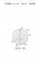
- FIG. 5is a bottom plan view of a typical split cell photodetector which may be utilized in the subject invention.
- FIGS. 1 and 2one of the more pressing problems relates to the semiconductor industry and the detecting of residues produced during lithographic and etching processes.
- the importance of the problemis highlighted by the fact that even small amounts of residue left behind by either the lithography or etching process can lead to improperly functioning circuits.
- the difficulty of solving the problemcan be appreciated when viewing FIGS. 1 and 2.
- the residues which must be detectedlie in contacts or holes created on the substrate surface. These holes can have a width as small as 1 micron.
- any detecting techniquemust be capable of looking down into the holes, as indicated at arrows H1 and H2 in FIGS. 1 and 2, respectively.
- the subject inventionovercomes these problems by providing a system which can be accurately focused into these holes to detect residues.
- Another problemrelates to the evaluation of ion dopant concentrations at the surface of the sample as illustrated in FIG. 3.
- the subject inventionprovides a mechanism for solving both of these detection problems.
- FIG. 4there is illustrated the appratus 20 for carrying out the method of the subject invention.
- a substrate 22is shown which may be an integrated circuit or any other sample which needs to be evaluated.
- Sample 22is shown resting on a platform 24 capable of rastering the sample with respect to the detecting apparatus.
- Controllable stagesare well known in the art and are also disclosed in U.S. Pat. No. 4,255,971, cited above.
- the upper surface of the sampleis subjected to a periodic localized heating.
- this periodic localized heatingis provided by a laser 30 which is intensity modulated by modulator 32.
- the frequency of modulationis based on the electronics but is preferably greater than 50 kHz.
- the intensity modulated heating sourcecould be supplied by electromagnetic radiation at various wavelengths, including X-rays, gamma rays, infrared, ultraviolet, visible light, microwaves or radio frequencies.
- the intensity modulated sourcecan also be generated through thermal excitations arising from the interaction of the sample with an intensity modulated stream of particles, such as a beam of electrons, protons, neutrons, ions or molecules.
- an intensity modulated stream of particlessuch as a beam of electrons, protons, neutrons, ions or molecules.
- the intensity modulated beam 34is then passed through a dichroic mirror 36 and is preferably focused on a sample by a microscopic objective 38.
- the heating beamis an argon ion laser and the dichroic mirror is transparent to argon ion radiation.
- the dichroic mirrorfunctions to reflect the probe laser beam, which is preferably generated by a helium-neon laser.
- the periodic heating source disclosed aboveis identical to the type used in various thermal wave generation systems.
- the intensity modulated beamwill function to generate thermal waves in the sample.
- information about the thermal conductivity of the uppermost layers of the samplecan be determined by an analysis of the thermal waves generated in the sample.
- the reflectivity signalwill be affected by the thermal parameters of the sample as set forth in equation (2).
- a component of the reflectivity signal ⁇ R Twill represent the thermal characteristics of the layer. In that case, information about the layer may be determined by an analysis of the thermal waves.
- the layer of interestWhen the layer of interest is relatively thin, its thermal characteristics will not measurably affect the thermal parameters of the sample and thus will not measurably change the periodic surface temperature ⁇ T. However, if the layer is at least 5 Angstroms thick, the layer will still alter the temperature coefficient of reflectivity ( ⁇ R/ ⁇ T) of the sample. The latter phenomenon is taken advantage of in the subject invention to permit the evaluation of extremely thin layers due to the change in the temperature coefficient of reflectivity.
- the detection meansis defined by a light probe that emits a beam which is directed onto the surface of the sample that has been periodically heated by the modulated energy beam 34.
- the light probe beamis generated by a helium-neon laser 50.
- Various other sources of electromagnetic radiationmay be used for the probe beam as long as the beam reflectivity is affected by the temperature changes on the sample surface in a manner which can be measured.
- the probe beam 52 emanating from the helium-neon laser 50is then passed through a polarizing splitter 54.
- the polarizing splitteris oriented in such a manner as to let the coherent light emanating from laser 50 to pass freely therethrough. The splitter will, however, deflect all light whose phase has been rotated through 90° relative to beam 52. The reason for this arrangement will become apparent below.
- Waveplate 55functions to rotate the phase of the beam by 45°.
- the waveplatewill rotate the phase of the beam another 45° so that when it reaches splitter 54, the phase of the beam has been rotated a total of 90° from the incoming orientation.
- the splitter 54will deflect the retro-reflected light beam up to detector 56, as discussed in more detail below.
- the probe beam 52After the probe beam 52 initially passes through the waveplate, it is reflected downwardly by dichroic mirror 36.
- the dichroic mirroris transparent to argon ion light but will reflect the light rays in the helium-neon frequencies.
- the heating beam and the probe beamare aligned in a manner such that they are directed in a coincident manner down through lens 38 and focused at the same spot on the surface of the sample. By focusing the probe beam and the heating beam at the same spot, the maximum signal output can be achieved.
- the reflectivity signals of interestexist at any area on the surface of the sample which has been periodically heated by the beam 34. Therefore, the probe beam would not have to be directly coincident with the heating beam to detect the signals of interest. Accordingly, a microscope objective 38 is not necessary for focusing either the heating beam 34 or the probe beam 52. Rather, it is only necessary to direct the probe beam within at least a portion of the periodically heated area.
- a discussion and equations for calculating the size of the periodically heated areaare set forth in copending application Ser. No. 401,511, and now U.S. Pat. No. 4,521,118, issued June 4, 1985 and incorporated herein by reference. Briefly, the diameter of the heated area, extending radially away from the center of the heating beam, is a function of the diameter and frequency of the heating beam and the thermal parameters in the sample.
- the optical lens systemshould be capable of focusing the incoming heating and probe beams to a spot size of 1 micron in diameter.
- the probe beam 52impinges on the surface of the sample and interacts with the electrons and thus with the lattice structure of the sample.
- the lattice structure of the samplewill undergo periodic changes as the temperature of the sample changes periodically.
- the probe beamessentially "sees” the changes in this lattice structure and the level of reflectivity of the beam changes along with the changing thermal conditions of the sample surface.
- the probe beamis reflected back up to the dichroic mirror where it is, in turn, reflected back along the incoming beam path through the 1/4 ⁇ -waveplate 55.
- waveplate 55rotates the phase of the probe beam by another 45° such that when the beam reaches splitter 54, its phase has been rotated 90° with respect to the original beam.
- the splitterwill deflect the retro-reflected probe beam upwardly towards detector 56. Since intensity variations of the probe beam are to be detected, a standard photodetector may be employed as a sensing mechanism. The intensity variations which are measured are then supplied as an output signal to a processor 58 for evaluating the surface conditions of the sample.
- FIG. 5illustrates one type of standard photodetector 80 which is suitable for performing the intensity measurements of the subject invention.
- Photodetector 80is referred to as a split cell detector and can be used not only to measure variations in intensity of the probe beam (shown in phantom at 88) due to changes in periodic reflectivity of the sample, but can also be used to measure changes in the angular displacement of the probe beam.
- Thermal wave measurement by detection of the angular changes in a probe beamis described in U.S. Pat. No. 4,521,118, cited above.
- Split cell detector 80is defined by a photodetector having two sensing elements 82 and 84 located in a side-by-side arrangement separated by a divider 86 only a few microns thick. Each element 82, 84 generates an electrical signal proportional to the number of photons reaching that sector. Where the split cell is to be used to measure angular deviations of the probe beam, processor 58 functions to subtract the output of one sector from the output of the other. If, on the other hand, changes in reflectivity of the sample are to be measured, the output of elements 82 and 84 is summed.
- the output of detector 80(when measuring changes in reflectivity of the sample), will also be unaffected by the small changes in the diameter of the probe beam which may be induced by the periodic heating.
- periodic heating of a samplecan create a periodically changing thermal lens in the sample.
- the presence of the thermal lenscan be monitored by using a probe beam. For example, if a probe beam is passed, off-axis, through a periodically changing thermal lens, the beam will be periodically deflected. If the probe beam is passed through the center of thermal lens, its diameter will vary periodically by a small amount. The latter effect is described in U.S. Pat. No. 4,243,327, issued Jan. 6, 1981, to Frosch.
- the patent to Froschdescribes a method for detecting the changes in diameter of a reflected probe beam induced by a changing thermal lens. This method is based on the principle that as the probe beam varies in diameter, the number of photons striking a fixed area having a diameter that is smaller than the probe beam diameter, will vary over time. Thus, the detector in Frosch is designed to measure the number of photons striking a particular area over time, that is, the areal density of the photons at the detector surface.
- the detector 56(80), in combination with processor 58,is arranged to measure the total amount of photons reflected from the sample, without regard to the location at which the photons impact on the detector or the areal density of those photons at the detector surface.
- the output of detector 56is proportional to the number of photons reflected from the sample surface, the resulting signals will be unaffected by the small changes in the beam diameter which may be induced by the periodic heating.
- the measurement of intensity changes of the reflected probe beam due to changes in reflectivity of the sampleis independent of relatively small changes in both the position of the beam on the detector, as well as the diameter of the beam.
- detector 56 (80)is arranged so that the total amount of power in the reflected probe beam is measured. This measurement could not be accomplished if any portion of the probe beam moved off the surface of the detector. As can be appreciated, if part of the probe beam misses the detector surface, the output signals therefrom would not be proportional to the total number of photons in the reflected probe beam. Therefore, it is necessary that the apparatus be arranged such that the diameter of the probe beam underfills, or is less than, the active surface of the photodetector (i.e. falls within its boundary), as shown in FIG. 5.
- processor 58The operation of processor 58 is dependent on the type of testing configuration which is utilized. In all cases, however, the process is designed to evaluate the periodic intensity changes of the incoming probe beam which are the result of the reflectivity changes caused by the periodic heating on the sample. These high frequency changes are filtered to produce a signal which may be evaluated.
- the processormay be programmed with the value of a known signal, for example, an uncoated or untreated oxide. If residues are present, as for example, as shown in hole H1 of FIG. 1, the output signal measured will be different from the known, stored signal, indicating the presence of residues. Because the identity of a particular residue is rarely known, an evaluation of the thickness of residue layer would be quite difficult. However, in most manufacturing situations, only the detection of the presence of the residue is necessary.
- a samplecould be rastered with respect to the heating and probe beams.
- the movements of platform 24can be programmed in a manner to trace the paths defined by the etched tracks as shown in FIG. 2. If no residues remain, the output signal should remain constant. In contrast, any peaks or variations in the output signal will indicate the presence of residues.
- ion implanted dopantsWith ion implanted dopants more quantitative information can be obtained because the identity, and thus the thermal characteristics, of both the substrate and the dopant are known. For example, the output signals can be normalized against a known reference sample such that actual concentrations of the implanted dopants may be obtained. As discussed above, this system is capable of detecting dopant levels prior to the annealing process. Unlike electrical testing, which requires the dopant to be activated, the ions locked at the interstitial sites, prior to annealing, will nonetheless affect the temperature coefficient of reflectivity and therefore can be monitored.
- the subject inventionhas been shown to be capable of detecting boron ion dopant concentrations in silicon as low as 10 10 ions/cm 2 .
- This sensitivityis three orders of magnitude greater than the electrical testing available in the prior art.
- Analysiscan also be performed by rastering the sample relative to the heating and probe beams to generate one or two dimensional maps of dopant concentrations.
- a meansfor generating a localized periodic heating at the surface of the sample.
- the heating meansis an intensity modulated laser.
- the detection systemfurther includes a probe beam which is focused on the area periodically heated by the intensity modulated laser in a manner to reflect off the surface of the sample.
- a meansis provided for detecting the intensity variations of the reflected light resulting from the periodic heating. By processing the measured intensity variations of the reflected beam, surface conditions of the sample can be evaluated.
Landscapes
- General Health & Medical Sciences (AREA)
- Health & Medical Sciences (AREA)
- Life Sciences & Earth Sciences (AREA)
- Chemical & Material Sciences (AREA)
- Analytical Chemistry (AREA)
- Biochemistry (AREA)
- Physics & Mathematics (AREA)
- General Physics & Mathematics (AREA)
- Immunology (AREA)
- Pathology (AREA)
- Investigating Or Analysing Materials By Optical Means (AREA)
- Testing Or Measuring Of Semiconductors Or The Like (AREA)
- Investigating Or Analyzing Materials Using Thermal Means (AREA)
Abstract
Description
R.sub.T =R.sub.o +(δR/δT)(ΔT) (1)
ΔR.sub.T =(δR/δT)(ΔT) (2)
Claims (27)
Priority Applications (5)
| Application Number | Priority Date | Filing Date | Title |
|---|---|---|---|
| US06/612,076US4636088A (en) | 1984-05-21 | 1984-05-21 | Method and apparatus for evaluating surface conditions of a sample |
| JP60105732AJPS60256031A (en) | 1984-05-21 | 1985-05-17 | Method and device for evaluating state of surface of specimen |
| DE8585303509TDE3578824D1 (en) | 1984-05-21 | 1985-05-20 | METHOD AND DEVICE FOR EXAMINING THE SURFACE CONDITIONS OF A SAMPLE. |
| EP85303509AEP0162681B1 (en) | 1984-05-21 | 1985-05-20 | Method and apparatus for evaluating surface conditions of a sample |
| US07/550,333US5042952A (en) | 1984-05-21 | 1990-07-09 | Method and apparatus for evaluating surface and subsurface and subsurface features in a semiconductor |
Applications Claiming Priority (1)
| Application Number | Priority Date | Filing Date | Title |
|---|---|---|---|
| US06/612,076US4636088A (en) | 1984-05-21 | 1984-05-21 | Method and apparatus for evaluating surface conditions of a sample |
Related Child Applications (1)
| Application Number | Title | Priority Date | Filing Date |
|---|---|---|---|
| US70748585AContinuation-In-Part | 1984-05-21 | 1985-03-01 |
Publications (1)
| Publication Number | Publication Date |
|---|---|
| US4636088Atrue US4636088A (en) | 1987-01-13 |
Family
ID=24451619
Family Applications (1)
| Application Number | Title | Priority Date | Filing Date |
|---|---|---|---|
| US06/612,076Expired - LifetimeUS4636088A (en) | 1984-05-21 | 1984-05-21 | Method and apparatus for evaluating surface conditions of a sample |
Country Status (4)
| Country | Link |
|---|---|
| US (1) | US4636088A (en) |
| EP (1) | EP0162681B1 (en) |
| JP (1) | JPS60256031A (en) |
| DE (1) | DE3578824D1 (en) |
Cited By (74)
| Publication number | Priority date | Publication date | Assignee | Title |
|---|---|---|---|---|
| US4795260A (en)* | 1987-05-15 | 1989-01-03 | Therma-Wave, Inc. | Apparatus for locating and testing areas of interest on a workpiece |
| US4854710A (en)* | 1985-03-01 | 1989-08-08 | Therma-Wave, Inc. | Method and apparatus for evaluating surface and subsurface features in a semiconductor |
| US4921348A (en)* | 1989-01-26 | 1990-05-01 | Iowa State University Research Foundation, Inc. | Method and means for a spatial and temporal probe for laser-generated plumes based on density gradients |
| US4927766A (en)* | 1986-05-27 | 1990-05-22 | The Boc Group, Inc. | Gas constituent measurement and recording |
| US4952063A (en)* | 1985-03-01 | 1990-08-28 | Therma-Wave, Inc. | Method and apparatus for evaluating surface and subsurface features in a semiconductor |
| DE4037391A1 (en)* | 1989-12-28 | 1991-07-04 | Jenoptik Jena Gmbh | ARRANGEMENT FOR THERMAL WAVE ANALYSIS OF LAYERING SYSTEMS |
| DE4035266A1 (en)* | 1990-11-02 | 1992-05-07 | Jenoptik Jena Gmbh | METHOD AND ARRANGEMENT FOR THERMAL WAVE ANALYSIS |
| US5136172A (en)* | 1989-08-16 | 1992-08-04 | Hitachi, Ltd. | Method and apparatus for detecting photoacoustic signal |
| US5221142A (en)* | 1991-05-20 | 1993-06-22 | Peak Systems, Inc. | Method and apparatus for temperature measurement using thermal expansion |
| US5228776A (en)* | 1992-05-06 | 1993-07-20 | Therma-Wave, Inc. | Apparatus for evaluating thermal and electrical characteristics in a sample |
| US5229304A (en)* | 1992-05-04 | 1993-07-20 | At&T Bell Laboratories | Method for manufacturing a semiconductor device, including optical inspection |
| US5258612A (en)* | 1992-04-01 | 1993-11-02 | Clark William G | Timed-resolved spectroscopy with split pump and probe pulses |
| DE4223337A1 (en)* | 1992-07-16 | 1994-01-20 | Jenoptik Jena Gmbh | Process and arrangement for photothermal spectroscopy |
| US5349399A (en)* | 1992-04-03 | 1994-09-20 | Kabushiki Kaisha Topcon | Intraocular length measuring instrument having phase compensating means |
| US5406378A (en)* | 1992-04-29 | 1995-04-11 | Mpb Technologies Inc. | Method and apparatus for non-contact and rapid identification of wood species |
| US5479259A (en)* | 1991-05-20 | 1995-12-26 | Hitachi, Ltd. | Method and apparatus for detecting photoacoustic signal |
| US5574562A (en)* | 1994-12-19 | 1996-11-12 | The Board Of Trustees Of The Leland Stanford Junior University | Method and apparatus for evaluation of high temperature superconductors |
| US5604592A (en)* | 1994-09-19 | 1997-02-18 | Textron Defense Systems, Division Of Avco Corporation | Laser ultrasonics-based material analysis system and method using matched filter processing |
| US5657754A (en)* | 1995-07-10 | 1997-08-19 | Rosencwaig; Allan | Apparatus for non-invasive analyses of biological compounds |
| US5706094A (en)* | 1995-08-25 | 1998-01-06 | Brown University Research Foundation | Ultrafast optical technique for the characterization of altered materials |
| US5748317A (en)* | 1997-01-21 | 1998-05-05 | Brown University Research Foundation | Apparatus and method for characterizing thin film and interfaces using an optical heat generator and detector |
| US5748318A (en)* | 1996-01-23 | 1998-05-05 | Brown University Research Foundation | Optical stress generator and detector |
| US5844684A (en)* | 1997-02-28 | 1998-12-01 | Brown University Research Foundation | Optical method for determining the mechanical properties of a material |
| US5864393A (en)* | 1997-07-30 | 1999-01-26 | Brown University Research Foundation | Optical method for the determination of stress in thin films |
| US5978074A (en)* | 1997-07-03 | 1999-11-02 | Therma-Wave, Inc. | Apparatus for evaluating metalized layers on semiconductors |
| US6008906A (en)* | 1995-08-25 | 1999-12-28 | Brown University Research Foundation | Optical method for the characterization of the electrical properties of semiconductors and insulating films |
| US6025918A (en)* | 1998-07-07 | 2000-02-15 | Brown University Research Foundation | Apparatus and method for measurement of the mechanical properties and electromigration of thin films |
| US6038026A (en)* | 1998-07-07 | 2000-03-14 | Brown University Research Foundation | Apparatus and method for the determination of grain size in thin films |
| US6049220A (en)* | 1998-06-10 | 2000-04-11 | Boxer Cross Incorporated | Apparatus and method for evaluating a wafer of semiconductor material |
| US6054868A (en)* | 1998-06-10 | 2000-04-25 | Boxer Cross Incorporated | Apparatus and method for measuring a property of a layer in a multilayered structure |
| US6095679A (en)* | 1996-04-22 | 2000-08-01 | Ta Instruments | Method and apparatus for performing localized thermal analysis and sub-surface imaging by scanning thermal microscopy |
| US6108087A (en)* | 1998-02-24 | 2000-08-22 | Kla-Tencor Corporation | Non-contact system for measuring film thickness |
| US6175416B1 (en) | 1996-08-06 | 2001-01-16 | Brown University Research Foundation | Optical stress generator and detector |
| US6317216B1 (en) | 1999-12-13 | 2001-11-13 | Brown University Research Foundation | Optical method for the determination of grain orientation in films |
| US6321601B1 (en) | 1996-08-06 | 2001-11-27 | Brown University Research Foundation | Optical method for the characterization of laterally-patterned samples in integrated circuits |
| US6408048B2 (en) | 2000-03-14 | 2002-06-18 | Therma-Wave, Inc. | Apparatus for analyzing samples using combined thermal wave and X-ray reflectance measurements |
| US6439764B1 (en)* | 1999-06-17 | 2002-08-27 | Daimlerchrysler Ag | Device and process for thermographic examination of functional surfaces of forming tools |
| US20020151092A1 (en)* | 2001-02-16 | 2002-10-17 | Jiping Li | Evaluating sidewall coverage in a semiconductor wafer |
| US20020171845A1 (en)* | 1998-06-30 | 2002-11-21 | Drake Thomas E. | System and method for controlling wafer temperature |
| US6532070B1 (en) | 2000-07-17 | 2003-03-11 | Therma-Wave, Inc. | Method for determining ion concentration and energy of shallow junction implants |
| US6535285B1 (en) | 2000-02-08 | 2003-03-18 | Therma-Wave, Inc. | Combination thermal wave and optical spectroscopy measurement system |
| US20030071994A1 (en)* | 2001-10-09 | 2003-04-17 | Peter G. Borden | Calibration as well as measurement on the same workpiece during fabrication |
| US6552803B1 (en) | 1998-02-24 | 2003-04-22 | Kla-Tencor Corporation | Detection of film thickness through induced acoustic pulse-echos |
| US20030165178A1 (en)* | 2002-03-01 | 2003-09-04 | Borden Peter G. | Identifying defects in a conductive structure of a wafer, based on heat transfer therethrough |
| US20030164946A1 (en)* | 2002-03-01 | 2003-09-04 | Borden Peter G. | Apparatus and method for measuring a property of a layer in a multilayered structure |
| US20030202556A1 (en)* | 2002-04-30 | 2003-10-30 | Naoyuki Taketoshi | Method of measuring fast time response using fast pulse and system of the same |
| US6654488B1 (en)* | 1999-07-01 | 2003-11-25 | International Business Machines Corporation | Fill pattern inspection |
| US20030234932A1 (en)* | 2002-06-21 | 2003-12-25 | Lena Nicolaides | Modulated reflectance measurement system with multiple wavelengths |
| US20040032679A1 (en)* | 2002-08-14 | 2004-02-19 | Tzenka Miteva | Method of determining the temperature in a system |
| US6696692B1 (en)* | 2000-11-06 | 2004-02-24 | Hrl Laboratories, Llc | Process control methods for use with e-beam fabrication technology |
| US20040057052A1 (en)* | 2002-09-23 | 2004-03-25 | Borden Peter G | Measurement of lateral diffusion of diffused layers |
| US20040063225A1 (en)* | 2002-09-23 | 2004-04-01 | Borden Peter G. | Measurement of lateral diffusion of diffused layers |
| US20040104352A1 (en)* | 2002-09-23 | 2004-06-03 | Jon Opsal | Modulated reflectance measurement system using UV probe |
| US20040136003A1 (en)* | 2003-01-09 | 2004-07-15 | Smith Walter Lee | Scatterometry for junction metrology |
| US20040169859A1 (en)* | 2003-02-28 | 2004-09-02 | Smith Walter Lee | Modulated scatterometry |
| US20040189993A1 (en)* | 2003-03-31 | 2004-09-30 | Martin Ebert | System for performing ellipsometry using an auxiliary pump beam to reduce effective illumination spot size |
| US6812047B1 (en) | 2000-03-08 | 2004-11-02 | Boxer Cross, Inc. | Evaluating a geometric or material property of a multilayered structure |
| US20040239945A1 (en)* | 1999-03-22 | 2004-12-02 | Borden Peter G. | Apparatus and method for determining the active dopant profile in a semiconductor wafer |
| US20040253751A1 (en)* | 2003-06-16 | 2004-12-16 | Alex Salnik | Photothermal ultra-shallow junction monitoring system with UV pump |
| US20040251927A1 (en)* | 2003-06-10 | 2004-12-16 | Alex Salnik | Characterization of ultra shallow junctions in semiconductor wafers |
| US20050036136A1 (en)* | 2003-08-14 | 2005-02-17 | Jon Opsal | Position modulated optical reflectance measurement system for semiconductor metrology |
| US20050062971A1 (en)* | 2003-09-24 | 2005-03-24 | Alex Salnik | Photothermal system with spectroscopic pump and probe |
| US20050083528A1 (en)* | 2002-03-18 | 2005-04-21 | Alex Salnik | ION implant monitoring through measurement of modulated optical response |
| US6885444B2 (en) | 1998-06-10 | 2005-04-26 | Boxer Cross Inc | Evaluating a multi-layered structure for voids |
| US20050088187A1 (en)* | 2001-03-05 | 2005-04-28 | Applied Materials, Inc. | Use of coefficient of a power curve to evaluate a semiconductor wafer |
| US20050184257A1 (en)* | 2004-02-20 | 2005-08-25 | Applied Materials, Inc. | Characterizing an electron beam treatment apparatus |
| KR100512005B1 (en)* | 2002-11-28 | 2005-09-02 | 삼성전자주식회사 | Method and apparatus for detecting contamination in an ion-implanted wafer |
| US20050214956A1 (en)* | 2004-03-29 | 2005-09-29 | Applied Materials, Inc. | High throughput measurement of via defects in interconnects |
| US20060012791A1 (en)* | 2004-06-22 | 2006-01-19 | Silviu Reinhorn | Wafer inspection system |
| US20070188761A1 (en)* | 2006-02-14 | 2007-08-16 | Alex Salnik | Combined modulated optical reflectance and electrical system for ultra-shallow junctions applications |
| US20080036998A1 (en)* | 2006-08-10 | 2008-02-14 | Alex Salnik | Probe beam profile modulated optical reflectance system and methods |
| US7379185B2 (en) | 2004-11-01 | 2008-05-27 | Applied Materials, Inc. | Evaluation of openings in a dielectric layer |
| US20080318345A1 (en)* | 2007-06-22 | 2008-12-25 | Persing Harold M | Plasma ion implantation process control using reflectometry |
| US20220412896A1 (en)* | 2019-12-05 | 2022-12-29 | Aurora Solar Technologies (Canada) Inc. | Systems and methods of characterizing semiconductor materials |
Families Citing this family (7)
| Publication number | Priority date | Publication date | Assignee | Title |
|---|---|---|---|---|
| US4652757A (en)* | 1985-08-02 | 1987-03-24 | At&T Technologies, Inc. | Method and apparatus for optically determining defects in a semiconductor material |
| US4750822A (en)* | 1986-03-28 | 1988-06-14 | Therma-Wave, Inc. | Method and apparatus for optically detecting surface states in materials |
| US5074669A (en)* | 1989-12-12 | 1991-12-24 | Therma-Wave, Inc. | Method and apparatus for evaluating ion implant dosage levels in semiconductors |
| DE19819144C1 (en)* | 1998-04-29 | 2000-06-15 | Tga Tech Geraete Und Apparateb | Microscopic investigation of implant integration into living tissues is carried out by automatically-scanning confocal laser microscope, digitizing image plane data to assemble three dimensional display |
| AU2001284910B2 (en) | 2000-08-16 | 2007-03-22 | Dolby Laboratories Licensing Corporation | Modulating one or more parameters of an audio or video perceptual coding system in response to supplemental information |
| GB0427318D0 (en)* | 2004-12-14 | 2005-01-19 | Imec Inter Uni Micro Electr | Method and device for the independent extraction of carrier concentration level and electrical junction depth in a semiconductor substrate |
| JP5702545B2 (en)* | 2009-03-17 | 2015-04-15 | アイメックImec | Method and apparatus for measuring the junction depth of a semiconductor region |
Citations (9)
| Publication number | Priority date | Publication date | Assignee | Title |
|---|---|---|---|---|
| US3462602A (en)* | 1967-08-16 | 1969-08-19 | Automation Ind Inc | Infra-red flaw detector |
| US3930730A (en)* | 1972-09-06 | 1976-01-06 | Republic Of France | Interferometric device for measurement of variations in length of a sample under the influence of temperature |
| US4243327A (en)* | 1979-01-31 | 1981-01-06 | Nasa | Double-beam optical method and apparatus for measuring thermal diffusivity and other molecular dynamic processes in utilizing the transient thermal lens effect |
| US4255971A (en)* | 1978-11-01 | 1981-03-17 | Allan Rosencwaig | Thermoacoustic microscopy |
| US4358201A (en)* | 1979-06-22 | 1982-11-09 | International Business Machines Corporation | Interferometric measurement apparatus and method having increased measuring range |
| US4446719A (en)* | 1982-07-22 | 1984-05-08 | General Motors Corporation | Electroreflectance vibrational spectroscopy |
| US4455741A (en)* | 1982-02-11 | 1984-06-26 | At&T Bell Laboratories | Fabrication of solid state electronic devices using fluorescent imaging of surface temperature profiles |
| US4468136A (en)* | 1982-02-12 | 1984-08-28 | The Johns Hopkins University | Optical beam deflection thermal imaging |
| US4579463A (en)* | 1984-05-21 | 1986-04-01 | Therma-Wave Partners | Detecting thermal waves to evaluate thermal parameters |
Family Cites Families (1)
| Publication number | Priority date | Publication date | Assignee | Title |
|---|---|---|---|---|
| US4521118A (en)* | 1982-07-26 | 1985-06-04 | Therma-Wave, Inc. | Method for detection of thermal waves with a laser probe |
- 1984
- 1984-05-21USUS06/612,076patent/US4636088A/ennot_activeExpired - Lifetime
- 1985
- 1985-05-17JPJP60105732Apatent/JPS60256031A/enactiveGranted
- 1985-05-20EPEP85303509Apatent/EP0162681B1/ennot_activeExpired
- 1985-05-20DEDE8585303509Tpatent/DE3578824D1/ennot_activeExpired - Lifetime
Patent Citations (9)
| Publication number | Priority date | Publication date | Assignee | Title |
|---|---|---|---|---|
| US3462602A (en)* | 1967-08-16 | 1969-08-19 | Automation Ind Inc | Infra-red flaw detector |
| US3930730A (en)* | 1972-09-06 | 1976-01-06 | Republic Of France | Interferometric device for measurement of variations in length of a sample under the influence of temperature |
| US4255971A (en)* | 1978-11-01 | 1981-03-17 | Allan Rosencwaig | Thermoacoustic microscopy |
| US4243327A (en)* | 1979-01-31 | 1981-01-06 | Nasa | Double-beam optical method and apparatus for measuring thermal diffusivity and other molecular dynamic processes in utilizing the transient thermal lens effect |
| US4358201A (en)* | 1979-06-22 | 1982-11-09 | International Business Machines Corporation | Interferometric measurement apparatus and method having increased measuring range |
| US4455741A (en)* | 1982-02-11 | 1984-06-26 | At&T Bell Laboratories | Fabrication of solid state electronic devices using fluorescent imaging of surface temperature profiles |
| US4468136A (en)* | 1982-02-12 | 1984-08-28 | The Johns Hopkins University | Optical beam deflection thermal imaging |
| US4446719A (en)* | 1982-07-22 | 1984-05-08 | General Motors Corporation | Electroreflectance vibrational spectroscopy |
| US4579463A (en)* | 1984-05-21 | 1986-04-01 | Therma-Wave Partners | Detecting thermal waves to evaluate thermal parameters |
Non-Patent Citations (8)
| Title |
|---|
| "Ion Implant Monitoring with Thermal Wave Technology", Smith et al., pp. 584-586, Applied Phys. Letters 47(6), 15 Sep. '85. |
| "Non-Destructive Interferometric Detection of Unbonded Layers", by P. Cielo, pp. 231-248, reprint of Optics & Lasers in Engineering, 1/14/84. |
| "Thermal & Plasma Wave Depth Profiling in Silicon", (Opsal et al) pp. 498-500, Applied Phys. Letters 47(5), 1/9/85. |
| "Thermal Wave Detection & Thin-Film Thickness Measurements with Laser Beam Detection", Jon Opsal, Rosencwaig, et al, Applied Optics, 10/15/83, vol. 22, No. 20, pp. 3169-3176. |
| Ion Implant Monitoring with Thermal Wave Technology , Smith et al., pp. 584 586, Applied Phys. Letters 47(6), 15 Sep. 85.* |
| Non Destructive Interferometric Detection of Unbonded Layers , by P. Cielo, pp. 231 248, reprint of Optics & Lasers in Engineering, 1/14/84.* |
| Thermal & Plasma Wave Depth Profiling in Silicon , (Opsal et al) pp. 498 500, Applied Phys. Letters 47(5), 1/9/85.* |
| Thermal Wave Detection & Thin Film Thickness Measurements with Laser Beam Detection , Jon Opsal, Rosencwaig, et al, Applied Optics, 10/15/83, vol. 22, No. 20, pp. 3169 3176.* |
Cited By (165)
| Publication number | Priority date | Publication date | Assignee | Title |
|---|---|---|---|---|
| US4854710A (en)* | 1985-03-01 | 1989-08-08 | Therma-Wave, Inc. | Method and apparatus for evaluating surface and subsurface features in a semiconductor |
| US4952063A (en)* | 1985-03-01 | 1990-08-28 | Therma-Wave, Inc. | Method and apparatus for evaluating surface and subsurface features in a semiconductor |
| US4927766A (en)* | 1986-05-27 | 1990-05-22 | The Boc Group, Inc. | Gas constituent measurement and recording |
| US4795260A (en)* | 1987-05-15 | 1989-01-03 | Therma-Wave, Inc. | Apparatus for locating and testing areas of interest on a workpiece |
| US4921348A (en)* | 1989-01-26 | 1990-05-01 | Iowa State University Research Foundation, Inc. | Method and means for a spatial and temporal probe for laser-generated plumes based on density gradients |
| US5136172A (en)* | 1989-08-16 | 1992-08-04 | Hitachi, Ltd. | Method and apparatus for detecting photoacoustic signal |
| DE4037391A1 (en)* | 1989-12-28 | 1991-07-04 | Jenoptik Jena Gmbh | ARRANGEMENT FOR THERMAL WAVE ANALYSIS OF LAYERING SYSTEMS |
| DE4035266A1 (en)* | 1990-11-02 | 1992-05-07 | Jenoptik Jena Gmbh | METHOD AND ARRANGEMENT FOR THERMAL WAVE ANALYSIS |
| US5206710A (en)* | 1990-11-02 | 1993-04-27 | Jenoptik Jena Gmbh | Method and apparatus for thermowave analysis |
| US5221142A (en)* | 1991-05-20 | 1993-06-22 | Peak Systems, Inc. | Method and apparatus for temperature measurement using thermal expansion |
| US5479259A (en)* | 1991-05-20 | 1995-12-26 | Hitachi, Ltd. | Method and apparatus for detecting photoacoustic signal |
| US5258612A (en)* | 1992-04-01 | 1993-11-02 | Clark William G | Timed-resolved spectroscopy with split pump and probe pulses |
| US5349399A (en)* | 1992-04-03 | 1994-09-20 | Kabushiki Kaisha Topcon | Intraocular length measuring instrument having phase compensating means |
| US5406378A (en)* | 1992-04-29 | 1995-04-11 | Mpb Technologies Inc. | Method and apparatus for non-contact and rapid identification of wood species |
| US5229304A (en)* | 1992-05-04 | 1993-07-20 | At&T Bell Laboratories | Method for manufacturing a semiconductor device, including optical inspection |
| US5228776A (en)* | 1992-05-06 | 1993-07-20 | Therma-Wave, Inc. | Apparatus for evaluating thermal and electrical characteristics in a sample |
| DE4223337A1 (en)* | 1992-07-16 | 1994-01-20 | Jenoptik Jena Gmbh | Process and arrangement for photothermal spectroscopy |
| US5604592A (en)* | 1994-09-19 | 1997-02-18 | Textron Defense Systems, Division Of Avco Corporation | Laser ultrasonics-based material analysis system and method using matched filter processing |
| US5638396A (en)* | 1994-09-19 | 1997-06-10 | Textron Systems Corporation | Laser ultrasonics-based material analysis system and method |
| US5574562A (en)* | 1994-12-19 | 1996-11-12 | The Board Of Trustees Of The Leland Stanford Junior University | Method and apparatus for evaluation of high temperature superconductors |
| US5657754A (en)* | 1995-07-10 | 1997-08-19 | Rosencwaig; Allan | Apparatus for non-invasive analyses of biological compounds |
| US5706094A (en)* | 1995-08-25 | 1998-01-06 | Brown University Research Foundation | Ultrafast optical technique for the characterization of altered materials |
| US6008906A (en)* | 1995-08-25 | 1999-12-28 | Brown University Research Foundation | Optical method for the characterization of the electrical properties of semiconductors and insulating films |
| US6211961B1 (en) | 1995-08-25 | 2001-04-03 | Brown University Research Foundation | Optical method for the characterization of the electrical properties of semiconductors and insulating films |
| US6208421B1 (en) | 1996-01-23 | 2001-03-27 | Brown University Research Foundation | Optical stress generator and detector |
| US5748318A (en)* | 1996-01-23 | 1998-05-05 | Brown University Research Foundation | Optical stress generator and detector |
| US6271921B1 (en) | 1996-01-23 | 2001-08-07 | Brown University Research Foundation | Optical stress generator and detector |
| US5959735A (en)* | 1996-01-23 | 1999-09-28 | Brown University Research Foundation | Optical stress generator and detector |
| US7339676B2 (en) | 1996-01-23 | 2008-03-04 | Brown University | Optical method and system for the characterization of laterally-patterned samples in integrated circuits |
| US6400449B2 (en) | 1996-01-23 | 2002-06-04 | Brown University Research Foundation | Optical stress generator and detector |
| US6491425B1 (en)* | 1996-04-22 | 2002-12-10 | Ta Instruments, Inc. | Method and apparatus for performing localized thermal analysis and sub-surface imaging by scanning thermal microscopy |
| US6095679A (en)* | 1996-04-22 | 2000-08-01 | Ta Instruments | Method and apparatus for performing localized thermal analysis and sub-surface imaging by scanning thermal microscopy |
| US7505154B2 (en) | 1996-08-06 | 2009-03-17 | Brown University | Optical method for the characterization of laterally patterned samples in integrated circuits |
| US7894070B2 (en) | 1996-08-06 | 2011-02-22 | Brown University | Optical method and system for the characterization of laterally-patterned samples in integrated circuits |
| US20080151219A1 (en)* | 1996-08-06 | 2008-06-26 | Brown University Research Foundation | Optical method for the characterization of laterally patterned samples in integrated circuits |
| US6175416B1 (en) | 1996-08-06 | 2001-01-16 | Brown University Research Foundation | Optical stress generator and detector |
| US7782471B2 (en) | 1996-08-06 | 2010-08-24 | Brown University | Optical method for the characterization of laterally-patterned samples in integrated circuits |
| US6321601B1 (en) | 1996-08-06 | 2001-11-27 | Brown University Research Foundation | Optical method for the characterization of laterally-patterned samples in integrated circuits |
| US5748317A (en)* | 1997-01-21 | 1998-05-05 | Brown University Research Foundation | Apparatus and method for characterizing thin film and interfaces using an optical heat generator and detector |
| US5844684A (en)* | 1997-02-28 | 1998-12-01 | Brown University Research Foundation | Optical method for determining the mechanical properties of a material |
| US6452685B2 (en) | 1997-07-03 | 2002-09-17 | Therma-Wave, Inc. | Apparatus for evaluating metalized layers on semiconductors |
| US6522413B2 (en) | 1997-07-03 | 2003-02-18 | Therma-Wave, Inc. | Apparatus for evaluating metalized layers on semiconductors |
| US5978074A (en)* | 1997-07-03 | 1999-11-02 | Therma-Wave, Inc. | Apparatus for evaluating metalized layers on semiconductors |
| US6320666B1 (en) | 1997-07-03 | 2001-11-20 | Therma-Wave, Inc. | Apparatus for evaluating metalized layers on semiconductors |
| US6191846B1 (en) | 1997-07-03 | 2001-02-20 | Therma-Wave, Inc. | Apparatus for evaluating metalized layers on semiconductors |
| US20040174538A1 (en)* | 1997-07-03 | 2004-09-09 | Jon Opsal | Systems and methods for evaluating semiconductor layers |
| US20050162654A1 (en)* | 1997-07-03 | 2005-07-28 | Jon Opsal | Systems and methods for evaluating semiconductor layers |
| US6882424B2 (en) | 1997-07-03 | 2005-04-19 | Therma-Wave, Inc. | Systems and methods for evaluating semiconductor layers |
| US6836338B2 (en) | 1997-07-03 | 2004-12-28 | Therma-Wave, Inc. | Apparatus for evaluating metalized layers on semiconductors |
| US5864393A (en)* | 1997-07-30 | 1999-01-26 | Brown University Research Foundation | Optical method for the determination of stress in thin films |
| US6108087A (en)* | 1998-02-24 | 2000-08-22 | Kla-Tencor Corporation | Non-contact system for measuring film thickness |
| US6552803B1 (en) | 1998-02-24 | 2003-04-22 | Kla-Tencor Corporation | Detection of film thickness through induced acoustic pulse-echos |
| US6049220A (en)* | 1998-06-10 | 2000-04-11 | Boxer Cross Incorporated | Apparatus and method for evaluating a wafer of semiconductor material |
| US6054868A (en)* | 1998-06-10 | 2000-04-25 | Boxer Cross Incorporated | Apparatus and method for measuring a property of a layer in a multilayered structure |
| US6906801B2 (en) | 1998-06-10 | 2005-06-14 | Applied Materials, Inc. | Measuring a property of a layer in multilayered structure |
| US6885444B2 (en) | 1998-06-10 | 2005-04-26 | Boxer Cross Inc | Evaluating a multi-layered structure for voids |
| US20030085730A1 (en)* | 1998-06-10 | 2003-05-08 | Borden Peter G. | Apparatus and method for evaluating a wafer of semiconductor material |
| US20020171845A1 (en)* | 1998-06-30 | 2002-11-21 | Drake Thomas E. | System and method for controlling wafer temperature |
| US7612890B2 (en) | 1998-06-30 | 2009-11-03 | Lockheed Martin Corporation | System and method for controlling wafer temperature |
| US6208418B1 (en) | 1998-07-07 | 2001-03-27 | Brown University Research Foundation | Apparatus and method for measurement of the mechanical properties and electromigration of thin films |
| US6038026A (en)* | 1998-07-07 | 2000-03-14 | Brown University Research Foundation | Apparatus and method for the determination of grain size in thin films |
| US6025918A (en)* | 1998-07-07 | 2000-02-15 | Brown University Research Foundation | Apparatus and method for measurement of the mechanical properties and electromigration of thin films |
| US6191855B1 (en) | 1998-07-07 | 2001-02-20 | Brown University Research Foundation | Apparatus and method for the determination of grain size in thin films |
| US20040239945A1 (en)* | 1999-03-22 | 2004-12-02 | Borden Peter G. | Apparatus and method for determining the active dopant profile in a semiconductor wafer |
| US6885458B2 (en) | 1999-03-22 | 2005-04-26 | Applied Materials, Inc. | Apparatus and method for determining the active dopant profile in a semiconductor wafer |
| US6439764B1 (en)* | 1999-06-17 | 2002-08-27 | Daimlerchrysler Ag | Device and process for thermographic examination of functional surfaces of forming tools |
| US6654488B1 (en)* | 1999-07-01 | 2003-11-25 | International Business Machines Corporation | Fill pattern inspection |
| US6317216B1 (en) | 1999-12-13 | 2001-11-13 | Brown University Research Foundation | Optical method for the determination of grain orientation in films |
| US6563591B2 (en) | 1999-12-13 | 2003-05-13 | Brown University Research Foundation | Optical method for the determination of grain orientation in films |
| US6963401B2 (en) | 2000-02-08 | 2005-11-08 | Therma-Wave, Inc. | Combination thermal wave and optical spectroscopy measurement systems |
| US6535285B1 (en) | 2000-02-08 | 2003-03-18 | Therma-Wave, Inc. | Combination thermal wave and optical spectroscopy measurement system |
| US20040233435A1 (en)* | 2000-02-08 | 2004-11-25 | Jon Opsal | Combination thermal wave and optical spectroscopy measurement systems |
| US6671047B2 (en) | 2000-02-08 | 2003-12-30 | Therma-Wave, Inc. | Combination thermal wave and optical spectroscopy measurement systems |
| US20050088188A1 (en)* | 2000-03-08 | 2005-04-28 | Applied Materials, Inc. | Evaluating a property of a multilayered structure |
| US7465591B2 (en) | 2000-03-08 | 2008-12-16 | Applied Materials, Inc. | Evaluating a geometric or material property of a multilayered structure |
| US6812047B1 (en) | 2000-03-08 | 2004-11-02 | Boxer Cross, Inc. | Evaluating a geometric or material property of a multilayered structure |
| US6678349B2 (en) | 2000-03-14 | 2004-01-13 | Therma-Wave, Inc. | Apparatus for analyzing samples using combined thermal wave and X-ray reflectance measurements |
| US6408048B2 (en) | 2000-03-14 | 2002-06-18 | Therma-Wave, Inc. | Apparatus for analyzing samples using combined thermal wave and X-ray reflectance measurements |
| US6512815B2 (en) | 2000-03-14 | 2003-01-28 | Therma-Wave, Inc. | Apparatus for analyzing samples using combined thermal wave and X-ray reflectance measurements |
| US7099007B2 (en) | 2000-07-17 | 2006-08-29 | Therma-Wave, Inc. | Method for determining ion concentration and energy of shallow junction implants |
| US6665071B2 (en) | 2000-07-17 | 2003-12-16 | Therma-Wave, Inc. | Method for determining ion concentration and energy of shallow junction implants |
| US6532070B1 (en) | 2000-07-17 | 2003-03-11 | Therma-Wave, Inc. | Method for determining ion concentration and energy of shallow junction implants |
| US20050140976A1 (en)* | 2000-07-17 | 2005-06-30 | Minna Hovinen | Method for determining ion concentration and energy of shallow junction implants |
| US6859281B2 (en) | 2000-07-17 | 2005-02-22 | Therma-Wave, Inc. | Method for determining ion concentration and energy of shallow junction implants |
| US6696692B1 (en)* | 2000-11-06 | 2004-02-24 | Hrl Laboratories, Llc | Process control methods for use with e-beam fabrication technology |
| US20020151092A1 (en)* | 2001-02-16 | 2002-10-17 | Jiping Li | Evaluating sidewall coverage in a semiconductor wafer |
| US6911349B2 (en) | 2001-02-16 | 2005-06-28 | Boxer Cross Inc. | Evaluating sidewall coverage in a semiconductor wafer |
| US7130055B2 (en) | 2001-03-05 | 2006-10-31 | Applied Materials, Inc. | Use of coefficient of a power curve to evaluate a semiconductor wafer |
| US20050088187A1 (en)* | 2001-03-05 | 2005-04-28 | Applied Materials, Inc. | Use of coefficient of a power curve to evaluate a semiconductor wafer |
| US6940592B2 (en) | 2001-10-09 | 2005-09-06 | Applied Materials, Inc. | Calibration as well as measurement on the same workpiece during fabrication |
| US20030071994A1 (en)* | 2001-10-09 | 2003-04-17 | Peter G. Borden | Calibration as well as measurement on the same workpiece during fabrication |
| US20050264806A1 (en)* | 2001-10-09 | 2005-12-01 | Borden Peter G | Calibration as well as measurement on the same workpiece during fabrication |
| US7064822B2 (en) | 2002-03-01 | 2006-06-20 | Applied Materials, Inc. | Evaluating a multi-layered structure for voids |
| US7301619B2 (en) | 2002-03-01 | 2007-11-27 | Applied Materials, Inc. | Evaluating a multi-layered structure for voids |
| US20030165178A1 (en)* | 2002-03-01 | 2003-09-04 | Borden Peter G. | Identifying defects in a conductive structure of a wafer, based on heat transfer therethrough |
| US20030164946A1 (en)* | 2002-03-01 | 2003-09-04 | Borden Peter G. | Apparatus and method for measuring a property of a layer in a multilayered structure |
| US6971791B2 (en) | 2002-03-01 | 2005-12-06 | Boxer Cross, Inc | Identifying defects in a conductive structure of a wafer, based on heat transfer therethrough |
| US20060232768A1 (en)* | 2002-03-01 | 2006-10-19 | Borden Peter G | Evaluating a multi-layered structure for voids |
| WO2003075321A3 (en)* | 2002-03-01 | 2003-12-11 | Boxer Cross Inc | An apparatus and method for measuring a property of a layer in a multilayered structure |
| US6958814B2 (en)* | 2002-03-01 | 2005-10-25 | Applied Materials, Inc. | Apparatus and method for measuring a property of a layer in a multilayered structure |
| US20050186776A1 (en)* | 2002-03-01 | 2005-08-25 | Borden Peter G. | Evaluating a multi-layered structure for voids |
| US7141440B2 (en)* | 2002-03-01 | 2006-11-28 | Applied Materials, Inc. | Apparatus and method for measuring a property of a layer in a multilayered structure |
| US7088444B2 (en) | 2002-03-01 | 2006-08-08 | Applied Materials, Inc. | Evaluating a multi-layered structure for voids |
| US20050200850A1 (en)* | 2002-03-01 | 2005-09-15 | Borden Peter G. | Apparatus and method for measuring a property of a layer in a multilayered structure |
| US20050083528A1 (en)* | 2002-03-18 | 2005-04-21 | Alex Salnik | ION implant monitoring through measurement of modulated optical response |
| US7002690B2 (en) | 2002-03-18 | 2006-02-21 | Therma-Wave, Inc. | Ion implant monitoring through measurement of modulated optical response |
| US6989899B2 (en) | 2002-03-18 | 2006-01-24 | Therma-Wave, Inc. | Ion implant monitoring through measurement of modulated optical response |
| US20050190369A1 (en)* | 2002-03-18 | 2005-09-01 | Alex Salnik | Ion implant monitoring through measurement of modulated optical response |
| US20030202556A1 (en)* | 2002-04-30 | 2003-10-30 | Naoyuki Taketoshi | Method of measuring fast time response using fast pulse and system of the same |
| US7044636B2 (en)* | 2002-04-30 | 2006-05-16 | National Institute Of Advanced Industrial Science And Technology | Method of measuring fast time response using fast pulse and system of the same |
| WO2003096391A3 (en)* | 2002-05-09 | 2004-03-04 | Lockheed Corp | System and method for controlling wafer temperature |
| US20060262314A1 (en)* | 2002-06-21 | 2006-11-23 | Lena Nicolaides | Modulated reflectance measurement system with multiple wavelengths |
| US20080309943A1 (en)* | 2002-06-21 | 2008-12-18 | Lena Nicolaides | Modulated reflectance measurement system with multiple wavelengths |
| US20030234932A1 (en)* | 2002-06-21 | 2003-12-25 | Lena Nicolaides | Modulated reflectance measurement system with multiple wavelengths |
| US7116424B2 (en) | 2002-06-21 | 2006-10-03 | Therma-Wave, Inc. | Modulated reflectance measurement system with multiple wavelengths |
| US7619741B2 (en) | 2002-06-21 | 2009-11-17 | Kla-Tencor Corp. | Modulated reflectance measurement system with multiple wavelengths |
| US7106446B2 (en) | 2002-06-21 | 2006-09-12 | Therma-Wave, Inc. | Modulated reflectance measurement system with multiple wavelengths |
| US7423757B2 (en) | 2002-06-21 | 2008-09-09 | Kla-Tencor Corporation | Modulated reflectance measurement system with multiple wavelengths |
| US20060092425A1 (en)* | 2002-06-21 | 2006-05-04 | Lena Nicolaides | Modulated reflectance measurement system with multiple wavelengths |
| US20040032679A1 (en)* | 2002-08-14 | 2004-02-19 | Tzenka Miteva | Method of determining the temperature in a system |
| US7097354B2 (en)* | 2002-08-14 | 2006-08-29 | Sony Deutschland Gmbh | Method of determining the temperature in a system comprising a molecular heater fraction and a molecular thermometer fraction |
| US7126690B2 (en) | 2002-09-23 | 2006-10-24 | Therma-Wave, Inc. | Modulated reflectance measurement system using UV probe |
| US7362441B2 (en) | 2002-09-23 | 2008-04-22 | Kla-Tencor Corporation | Modulated reflectance measurement system using UV probe |
| US20080158565A1 (en)* | 2002-09-23 | 2008-07-03 | Jon Opsal | Modulated reflectance measurement system using uv probe |
| US20040063225A1 (en)* | 2002-09-23 | 2004-04-01 | Borden Peter G. | Measurement of lateral diffusion of diffused layers |
| US8817260B2 (en) | 2002-09-23 | 2014-08-26 | Kla-Tencor Corporation | Modulated reflectance measurement system using UV probe |
| US7646486B2 (en) | 2002-09-23 | 2010-01-12 | Kla-Tencor Corporation | Modulated reflectance measurement system using UV probe |
| US20070008541A1 (en)* | 2002-09-23 | 2007-01-11 | Jon Opsal | Modulated reflectance measurement system using UV probe |
| US20040104352A1 (en)* | 2002-09-23 | 2004-06-03 | Jon Opsal | Modulated reflectance measurement system using UV probe |
| US6963393B2 (en) | 2002-09-23 | 2005-11-08 | Applied Materials, Inc. | Measurement of lateral diffusion of diffused layers |
| US20040057052A1 (en)* | 2002-09-23 | 2004-03-25 | Borden Peter G | Measurement of lateral diffusion of diffused layers |
| KR100512005B1 (en)* | 2002-11-28 | 2005-09-02 | 삼성전자주식회사 | Method and apparatus for detecting contamination in an ion-implanted wafer |
| US20040136003A1 (en)* | 2003-01-09 | 2004-07-15 | Smith Walter Lee | Scatterometry for junction metrology |
| US6950190B2 (en) | 2003-01-09 | 2005-09-27 | Therma-Wave, Inc. | Scatterometry for junction metrology |
| US20040169859A1 (en)* | 2003-02-28 | 2004-09-02 | Smith Walter Lee | Modulated scatterometry |
| US20050168759A1 (en)* | 2003-02-28 | 2005-08-04 | Smith Walter L. | Modulated scatterometry |
| US7239390B2 (en) | 2003-02-28 | 2007-07-03 | Therma-Wave, Inc. | Modulated scatterometry |
| US20070188762A1 (en)* | 2003-02-28 | 2007-08-16 | Smith Walter L | Modulated scatterometry |
| US7400402B2 (en) | 2003-02-28 | 2008-07-15 | Kla-Tencor Corp. | Modulated scatterometry |
| US6888632B2 (en) | 2003-02-28 | 2005-05-03 | Therma-Wave, Inc. | Modulated scatterometry |
| US20040189993A1 (en)* | 2003-03-31 | 2004-09-30 | Martin Ebert | System for performing ellipsometry using an auxiliary pump beam to reduce effective illumination spot size |
| US6952261B2 (en) | 2003-03-31 | 2005-10-04 | Therma-Wave, Inc. | System for performing ellipsometry using an auxiliary pump beam to reduce effective measurement spot size |
| US7248367B2 (en) | 2003-06-10 | 2007-07-24 | Therma-Wave, Inc. | Characterization of ultra shallow junctions in semiconductor wafers |
| US20040251927A1 (en)* | 2003-06-10 | 2004-12-16 | Alex Salnik | Characterization of ultra shallow junctions in semiconductor wafers |
| US20040253751A1 (en)* | 2003-06-16 | 2004-12-16 | Alex Salnik | Photothermal ultra-shallow junction monitoring system with UV pump |
| US20050036136A1 (en)* | 2003-08-14 | 2005-02-17 | Jon Opsal | Position modulated optical reflectance measurement system for semiconductor metrology |
| US7212288B2 (en) | 2003-08-14 | 2007-05-01 | Therma-Wave, Inc. | Position modulated optical reflectance measurement system for semiconductor metrology |
| US7280215B2 (en) | 2003-09-24 | 2007-10-09 | Therma-Wave, Inc. | Photothermal system with spectroscopic pump and probe |
| US20050062971A1 (en)* | 2003-09-24 | 2005-03-24 | Alex Salnik | Photothermal system with spectroscopic pump and probe |
| WO2005083740A1 (en)* | 2004-02-20 | 2005-09-09 | Applied Materials, Inc. | Characterizing an electron beam treatment apparatus |
| US7045798B2 (en) | 2004-02-20 | 2006-05-16 | Applied Materials, Inc. | Characterizing an electron beam treatment apparatus |
| US20050184257A1 (en)* | 2004-02-20 | 2005-08-25 | Applied Materials, Inc. | Characterizing an electron beam treatment apparatus |
| US20050214956A1 (en)* | 2004-03-29 | 2005-09-29 | Applied Materials, Inc. | High throughput measurement of via defects in interconnects |
| US7026175B2 (en) | 2004-03-29 | 2006-04-11 | Applied Materials, Inc. | High throughput measurement of via defects in interconnects |
| US20060012791A1 (en)* | 2004-06-22 | 2006-01-19 | Silviu Reinhorn | Wafer inspection system |
| US20110141462A1 (en)* | 2004-06-22 | 2011-06-16 | Silviu Reinhorn | Wafer inspection system |
| US7379185B2 (en) | 2004-11-01 | 2008-05-27 | Applied Materials, Inc. | Evaluation of openings in a dielectric layer |
| US7499168B2 (en)* | 2006-02-14 | 2009-03-03 | Kla-Tencor Corp. | Combined modulated optical reflectance and electrical system for ultra-shallow junctions applications |
| US20070188761A1 (en)* | 2006-02-14 | 2007-08-16 | Alex Salnik | Combined modulated optical reflectance and electrical system for ultra-shallow junctions applications |
| US7502104B2 (en) | 2006-08-10 | 2009-03-10 | Kla-Tencor Corporation | Probe beam profile modulated optical reflectance system and methods |
| US20080036998A1 (en)* | 2006-08-10 | 2008-02-14 | Alex Salnik | Probe beam profile modulated optical reflectance system and methods |
| WO2009002762A1 (en)* | 2007-06-22 | 2008-12-31 | Varian Semiconductor Equipment Associates, Inc. | Plasma ion implantation process control using reflectometry |
| US20080318345A1 (en)* | 2007-06-22 | 2008-12-25 | Persing Harold M | Plasma ion implantation process control using reflectometry |
| US20220412896A1 (en)* | 2019-12-05 | 2022-12-29 | Aurora Solar Technologies (Canada) Inc. | Systems and methods of characterizing semiconductor materials |
| US12085516B2 (en)* | 2019-12-05 | 2024-09-10 | Aurora Solar Technologies (Canada) Inc. | Systems and methods of characterizing semiconductor materials |
Also Published As
| Publication number | Publication date |
|---|---|
| EP0162681A3 (en) | 1987-06-16 |
| JPS60256031A (en) | 1985-12-17 |
| DE3578824D1 (en) | 1990-08-30 |
| JPH0347704B2 (en) | 1991-07-22 |
| EP0162681A2 (en) | 1985-11-27 |
| EP0162681B1 (en) | 1990-07-25 |
Similar Documents
| Publication | Publication Date | Title |
|---|---|---|
| US4636088A (en) | Method and apparatus for evaluating surface conditions of a sample | |
| US4679946A (en) | Evaluating both thickness and compositional variables in a thin film sample | |
| US5228776A (en) | Apparatus for evaluating thermal and electrical characteristics in a sample | |
| US4634290A (en) | Method and apparatus for detecting thermal waves | |
| US4579463A (en) | Detecting thermal waves to evaluate thermal parameters | |
| EP0200301A1 (en) | Method and apparatus for evaluating surface and subsurface features in a semiconductor | |
| US6483594B2 (en) | Apparatus and method for determining the active dopant profile in a semiconductor wafer | |
| US8622612B2 (en) | Method and apparatus for determining the thermal expansion of a material | |
| US6052185A (en) | Method and apparatus for measuring the concentration of ions implanted in semiconductor materials | |
| US7141440B2 (en) | Apparatus and method for measuring a property of a layer in a multilayered structure | |
| US6462817B1 (en) | Method of monitoring ion implants by examination of an overlying masking material | |
| EP1118005A4 (en) | METHOD AND DEVICE FOR EVALUATING SEMICONDUCTOR DISCS | |
| JP2007305971A (en) | Overlay metrology using x-rays | |
| US5149978A (en) | Apparatus for measuring grain sizes in metalized layers | |
| JP4783801B2 (en) | Semiconductor inspection system and apparatus using non-vibrating contact potential difference sensor and controlled irradiation | |
| JP5009506B2 (en) | Method and system for determining one or more characteristics of a sample | |
| JP5239346B2 (en) | Stress evaluation method using Raman spectroscopy and semiconductor device manufacturing method | |
| KR20250123233A (en) | Inspection system | |
| JPH0755702A (en) | Crystal defect measuring apparatus and semiconductor manufacturing apparatus using the same | |
| TWI856467B (en) | Inspection device and film quality inspection method | |
| JPS61173171A (en) | Method for measuring resistivity of semiconductor wafer | |
| JPH0521566A (en) | Measuring method for ion implantation amount in semiconductor crystal | |
| EP4624911A1 (en) | A tool for analysing the chemical composition and structure of nanolayers | |
| JPH0233947A (en) | Ion implantation amount measurement method using infrared light scattering | |
| Bullis | Semiconductor Measurement Technology: Progress Report, January 1 to June 30, 1975 |
Legal Events
| Date | Code | Title | Description |
|---|---|---|---|
| AS | Assignment | Owner name:THERMA-WAVE PARTNERS Free format text:ASSIGNMENT OF ASSIGNORS INTEREST.;ASSIGNORS:ROSENCWAIG, ALLAN;SMITH, WALTER L.;REEL/FRAME:004304/0002 Effective date:19840706 | |
| AS | Assignment | Owner name:THERMA-WAVE, INC., A CORP OF CA. Free format text:ASSIGNMENT OF ASSIGNORS INTEREST.;ASSIGNOR:THERMA-WAVE PARTNERS;REEL/FRAME:004602/0285 Effective date:19860721 Owner name:THERMA-WAVE, INC., A CORP OF CA., STATELESS Free format text:ASSIGNMENT OF ASSIGNORS INTEREST;ASSIGNOR:THERMA-WAVE PARTNERS;REEL/FRAME:004602/0285 Effective date:19860721 | |
| STCF | Information on status: patent grant | Free format text:PATENTED CASE | |
| FEPP | Fee payment procedure | Free format text:PAYOR NUMBER ASSIGNED (ORIGINAL EVENT CODE: ASPN); ENTITY STATUS OF PATENT OWNER: LARGE ENTITY | |
| FPAY | Fee payment | Year of fee payment:4 | |
| AS | Assignment | Owner name:THERMA-WAVE, INC. A DE CORP., CALIFORNIA Free format text:ASSIGNMENT OF ASSIGNORS INTEREST.;ASSIGNOR:THERMA-WAVE, INC.;REEL/FRAME:006255/0853 Effective date:19920901 | |
| FEPP | Fee payment procedure | Free format text:PAT HLDR NO LONGER CLAIMS SMALL ENT STAT AS SMALL BUSINESS (ORIGINAL EVENT CODE: LSM2); ENTITY STATUS OF PATENT OWNER: LARGE ENTITY | |
| FPAY | Fee payment | Year of fee payment:8 | |
| AS | Assignment | Owner name:BANKERS TRUST COMPANY, NEW YORK Free format text:ASSIGNMENT OF SECURITY INTEREST;ASSIGNOR:THERME-WAVE, INC., A CORP. OF DELAWARE;REEL/FRAME:008519/0472 Effective date:19970516 | |
| CC | Certificate of correction | ||
| FPAY | Fee payment | Year of fee payment:12 | |
| AS | Assignment | Owner name:THERMA-WAVE, INC., CALIFORNIA Free format text:REASSIGNMENT AND RELEASE OF SECURITY INTEREST;ASSIGNOR:BANKERS TRUST COMPANY;REEL/FRAME:011855/0948 Effective date:20010420 | |
| AS | Assignment | Owner name:SILICON VALLEY BANK, CALIFORNIA Free format text:SECURITY AGREEMENT;ASSIGNOR:THERMA-WAVE, INC.;REEL/FRAME:014446/0150 Effective date:20030613 |