US4632057A - CVD plasma reactor - Google Patents
CVD plasma reactorDownload PDFInfo
- Publication number
- US4632057A US4632057AUS06/762,231US76223185AUS4632057AUS 4632057 AUS4632057 AUS 4632057AUS 76223185 AUS76223185 AUS 76223185AUS 4632057 AUS4632057 AUS 4632057A
- Authority
- US
- United States
- Prior art keywords
- set forth
- conductive member
- wafer
- temperature
- chamber
- Prior art date
- Legal status (The legal status is an assumption and is not a legal conclusion. Google has not performed a legal analysis and makes no representation as to the accuracy of the status listed.)
- Expired - Lifetime
Links
- 239000007789gasSubstances0.000claimsabstractdescription31
- 238000010438heat treatmentMethods0.000claimsabstractdescription11
- 238000005229chemical vapour depositionMethods0.000claimsabstractdescription4
- 239000004606Fillers/ExtendersSubstances0.000claimsdescription20
- 238000006243chemical reactionMethods0.000claimsdescription7
- 230000000694effectsEffects0.000claimsdescription2
- 230000005540biological transmissionEffects0.000claims1
- 238000005086pumpingMethods0.000claims1
- 238000000151depositionMethods0.000abstractdescription45
- 230000008021depositionEffects0.000abstractdescription42
- 239000004065semiconductorSubstances0.000abstractdescription6
- WQJQOUPTWCFRMM-UHFFFAOYSA-Ntungsten disilicideChemical group[Si]#[W]#[Si]WQJQOUPTWCFRMM-UHFFFAOYSA-N0.000abstractdescription4
- 235000012431wafersNutrition0.000description81
- 238000000034methodMethods0.000description21
- 230000008569processEffects0.000description21
- 238000001816coolingMethods0.000description8
- XUIMIQQOPSSXEZ-UHFFFAOYSA-NSiliconChemical compound[Si]XUIMIQQOPSSXEZ-UHFFFAOYSA-N0.000description6
- 239000000463materialSubstances0.000description6
- 229910052710siliconInorganic materials0.000description6
- 239000010703siliconSubstances0.000description6
- 230000032258transportEffects0.000description6
- MROCJMGDEKINLD-UHFFFAOYSA-NdichlorosilaneChemical compoundCl[SiH2]ClMROCJMGDEKINLD-UHFFFAOYSA-N0.000description5
- 239000010453quartzSubstances0.000description5
- VYPSYNLAJGMNEJ-UHFFFAOYSA-Nsilicon dioxideInorganic materialsO=[Si]=OVYPSYNLAJGMNEJ-UHFFFAOYSA-N0.000description5
- OKTJSMMVPCPJKN-UHFFFAOYSA-NCarbonChemical compound[C]OKTJSMMVPCPJKN-UHFFFAOYSA-N0.000description3
- 238000005137deposition processMethods0.000description3
- 229910002804graphiteInorganic materials0.000description3
- 239000010439graphiteSubstances0.000description3
- 230000005855radiationEffects0.000description3
- VXEGSRKPIUDPQT-UHFFFAOYSA-N4-[4-(4-methoxyphenyl)piperazin-1-yl]anilineChemical compoundC1=CC(OC)=CC=C1N1CCN(C=2C=CC(N)=CC=2)CC1VXEGSRKPIUDPQT-UHFFFAOYSA-N0.000description2
- 229910000809AlumelInorganic materials0.000description2
- BLRPTPMANUNPDV-UHFFFAOYSA-NSilaneChemical compound[SiH4]BLRPTPMANUNPDV-UHFFFAOYSA-N0.000description2
- XAGFODPZIPBFFR-UHFFFAOYSA-NaluminiumChemical compound[Al]XAGFODPZIPBFFR-UHFFFAOYSA-N0.000description2
- 229910052782aluminiumInorganic materials0.000description2
- 239000000919ceramicSubstances0.000description2
- 230000008859changeEffects0.000description2
- 238000011109contaminationMethods0.000description2
- 230000005684electric fieldEffects0.000description2
- 238000002156mixingMethods0.000description2
- 238000012544monitoring processMethods0.000description2
- 238000000623plasma-assisted chemical vapour depositionMethods0.000description2
- BASFCYQUMIYNBI-UHFFFAOYSA-NplatinumChemical compound[Pt]BASFCYQUMIYNBI-UHFFFAOYSA-N0.000description2
- 238000007789sealingMethods0.000description2
- 239000005049silicon tetrachlorideSubstances0.000description2
- 229910001220stainless steelInorganic materials0.000description2
- 239000010935stainless steelSubstances0.000description2
- 230000001360synchronised effectEffects0.000description2
- 238000012360testing methodMethods0.000description2
- 230000007723transport mechanismEffects0.000description2
- WFKWXMTUELFFGS-UHFFFAOYSA-NtungstenChemical compound[W]WFKWXMTUELFFGS-UHFFFAOYSA-N0.000description2
- 229910052721tungstenInorganic materials0.000description2
- 239000010937tungstenSubstances0.000description2
- 230000004913activationEffects0.000description1
- 229910021417amorphous siliconInorganic materials0.000description1
- 230000003321amplificationEffects0.000description1
- 239000006227byproductSubstances0.000description1
- 150000001875compoundsChemical class0.000description1
- 238000010276constructionMethods0.000description1
- 239000000112cooling gasSubstances0.000description1
- 230000001419dependent effectEffects0.000description1
- 230000001627detrimental effectEffects0.000description1
- BUMGIEFFCMBQDG-UHFFFAOYSA-NdichlorosiliconChemical compoundCl[Si]ClBUMGIEFFCMBQDG-UHFFFAOYSA-N0.000description1
- 238000010494dissociation reactionMethods0.000description1
- 230000005593dissociationsEffects0.000description1
- 238000005530etchingMethods0.000description1
- 238000002474experimental methodMethods0.000description1
- PCHJSUWPFVWCPO-UHFFFAOYSA-NgoldChemical compound[Au]PCHJSUWPFVWCPO-UHFFFAOYSA-N0.000description1
- 229910052737goldInorganic materials0.000description1
- 239000010931goldSubstances0.000description1
- 229910052736halogenInorganic materials0.000description1
- 150000002367halogensChemical class0.000description1
- 230000006872improvementEffects0.000description1
- 229910001026inconelInorganic materials0.000description1
- 239000011261inert gasSubstances0.000description1
- 150000002500ionsChemical class0.000description1
- 238000002955isolationMethods0.000description1
- 239000000203mixtureSubstances0.000description1
- 238000012986modificationMethods0.000description1
- 230000004048modificationEffects0.000description1
- 238000003199nucleic acid amplification methodMethods0.000description1
- 238000009832plasma treatmentMethods0.000description1
- UPIXZLGONUBZLK-UHFFFAOYSA-NplatinumChemical compound[Pt].[Pt]UPIXZLGONUBZLK-UHFFFAOYSA-N0.000description1
- 229910052697platinumInorganic materials0.000description1
- PXXKQOPKNFECSZ-UHFFFAOYSA-Nplatinum rhodiumChemical compound[Rh].[Pt]PXXKQOPKNFECSZ-UHFFFAOYSA-N0.000description1
- 238000012545processingMethods0.000description1
- 238000002310reflectometryMethods0.000description1
- 229910052703rhodiumInorganic materials0.000description1
- 239000010948rhodiumSubstances0.000description1
- MHOVAHRLVXNVSD-UHFFFAOYSA-Nrhodium atomChemical compound[Rh]MHOVAHRLVXNVSD-UHFFFAOYSA-N0.000description1
- 239000000523sampleSubstances0.000description1
- 229910000077silaneInorganic materials0.000description1
Images


Classifications
- C—CHEMISTRY; METALLURGY
- C23—COATING METALLIC MATERIAL; COATING MATERIAL WITH METALLIC MATERIAL; CHEMICAL SURFACE TREATMENT; DIFFUSION TREATMENT OF METALLIC MATERIAL; COATING BY VACUUM EVAPORATION, BY SPUTTERING, BY ION IMPLANTATION OR BY CHEMICAL VAPOUR DEPOSITION, IN GENERAL; INHIBITING CORROSION OF METALLIC MATERIAL OR INCRUSTATION IN GENERAL
- C23C—COATING METALLIC MATERIAL; COATING MATERIAL WITH METALLIC MATERIAL; SURFACE TREATMENT OF METALLIC MATERIAL BY DIFFUSION INTO THE SURFACE, BY CHEMICAL CONVERSION OR SUBSTITUTION; COATING BY VACUUM EVAPORATION, BY SPUTTERING, BY ION IMPLANTATION OR BY CHEMICAL VAPOUR DEPOSITION, IN GENERAL
- C23C16/00—Chemical coating by decomposition of gaseous compounds, without leaving reaction products of surface material in the coating, i.e. chemical vapour deposition [CVD] processes
- C23C16/44—Chemical coating by decomposition of gaseous compounds, without leaving reaction products of surface material in the coating, i.e. chemical vapour deposition [CVD] processes characterised by the method of coating
- C23C16/50—Chemical coating by decomposition of gaseous compounds, without leaving reaction products of surface material in the coating, i.e. chemical vapour deposition [CVD] processes characterised by the method of coating using electric discharges
- C23C16/505—Chemical coating by decomposition of gaseous compounds, without leaving reaction products of surface material in the coating, i.e. chemical vapour deposition [CVD] processes characterised by the method of coating using electric discharges using radio frequency discharges
- C23C16/509—Chemical coating by decomposition of gaseous compounds, without leaving reaction products of surface material in the coating, i.e. chemical vapour deposition [CVD] processes characterised by the method of coating using electric discharges using radio frequency discharges using internal electrodes
- C23C16/5096—Flat-bed apparatus
- C—CHEMISTRY; METALLURGY
- C23—COATING METALLIC MATERIAL; COATING MATERIAL WITH METALLIC MATERIAL; CHEMICAL SURFACE TREATMENT; DIFFUSION TREATMENT OF METALLIC MATERIAL; COATING BY VACUUM EVAPORATION, BY SPUTTERING, BY ION IMPLANTATION OR BY CHEMICAL VAPOUR DEPOSITION, IN GENERAL; INHIBITING CORROSION OF METALLIC MATERIAL OR INCRUSTATION IN GENERAL
- C23C—COATING METALLIC MATERIAL; COATING MATERIAL WITH METALLIC MATERIAL; SURFACE TREATMENT OF METALLIC MATERIAL BY DIFFUSION INTO THE SURFACE, BY CHEMICAL CONVERSION OR SUBSTITUTION; COATING BY VACUUM EVAPORATION, BY SPUTTERING, BY ION IMPLANTATION OR BY CHEMICAL VAPOUR DEPOSITION, IN GENERAL
- C23C16/00—Chemical coating by decomposition of gaseous compounds, without leaving reaction products of surface material in the coating, i.e. chemical vapour deposition [CVD] processes
- C23C16/44—Chemical coating by decomposition of gaseous compounds, without leaving reaction products of surface material in the coating, i.e. chemical vapour deposition [CVD] processes characterised by the method of coating
- C23C16/48—Chemical coating by decomposition of gaseous compounds, without leaving reaction products of surface material in the coating, i.e. chemical vapour deposition [CVD] processes characterised by the method of coating by irradiation, e.g. photolysis, radiolysis, particle radiation
- C23C16/481—Chemical coating by decomposition of gaseous compounds, without leaving reaction products of surface material in the coating, i.e. chemical vapour deposition [CVD] processes characterised by the method of coating by irradiation, e.g. photolysis, radiolysis, particle radiation by radiant heating of the substrate
Definitions
- This inventionrelates to plasma treatment of an article and, in particular, to plasma enhanced chemical vapor deposition (CVD).
- CVDplasma enhanced chemical vapor deposition
- Another source of difficultyin a sense, is the semiconductor industry itself.
- There is a constant demand for better resultse.g. uniformity, through-put, deposition rate. Improving both uniformity and deposition rate, for example, is not easy.
- there are several kinds of uniformityA first relates to the wafer itself.
- a third kindrelates to uniformity from batch to batch. For single wafer plasma reactors, the latter two are the same since the wafers are processed singly. As can be seen, improving one parameter may not be particularly difficult. Improving all of them is a feat.
- Another object of the present inventionis to provide an improved plasma deposition process in which both deposition rate and uniformity are improved for single wafer deposition in an automated vacuum load lock convertible for wafer diameters of 3-10 inches.
- a further object of the present inventionis to provide improved means for heating a semiconductor wafer.
- a further object of the present inventionis to provide improved means for controlling gas flow in a deposition chamber.
- Another object of the present inventionis to provide improved temperature sensing means for deposition apparatus.
- a further object of the present inventionis to provide improved control means for radiantly heating a wafer.
- Another object of the present inventionis to provide a process chamber compatible with vacuum transport apparatus.
- a plasma reactorcomprises a chamber having an annular baffle positioned to divide the chamber into an antechamber and a reaction chamber. Positioned about the periphery of the reaction chamber are gas supply and exhaust ports.
- the gas supply portsinclude extenders which project radially inwardly.
- An annular wallextends from the baffle into the reaction chamber. The extenders pass through the wall and are supported thereby.
- the baffleis separated from the periphery of the chamber by a gap.
- the bafflecomprises a central aperture. Gases can circulate between the antechamber and the reaction chamber through the gap and the aperture.
- the waferis held on a quartz window to which a heater means is attached.
- the heatercomprises lamps resiliently mounted on a conductive member but electrically isolated from the conductive member.
- Temperature sensing meansare mounted in the conductive member on the opposite side of the lamps from the wafer.
- the processis based upon the discovery that the plasma impedes deposition.
- the plasmais ignited for less than the whole deposition cycle.
- the waferis brought up to a predetermined temperature by applying full power to the lamps.
- the power to the lampsis reduced to an amount sufficient to maintain the temperature of the wafer.
- the deposition gasis supplied to the chamber and a plasma is ignited. The plasma is terminated and the deposition continues. After a predetermined length of time the deposition gas is stopped and the lamps are turned off. The wafer is then cooled and removed.
- FIG. 1illustrates a deposition chamber in accordance with the present invention.
- FIG. 2illustrates a portion of the temperature sensor in accordance with the present invention.
- FIG. 3illustrates a portion of the baffle and extenders in accordance with the present invention.
- FIG. 4illustrates the orientation of the extenders in accordance with the present invention.
- FIG. 5illustrates an alternative embodiment of a deposition chamber in accordance with the present invention.
- FIG. 6illustrates a deposition process in accordance with the present invention.
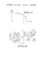
- FIG. 7illustrates a gas deposition characteristic used in the present invention.
- FIG. 8illustrates temperature sensing in accordance with the present invention.
- FIG. 9illustrates control circuitry in accordance with the present invention.
- FIG. 1illustrates a preferred embodiment of a reactor chamber for plasma enhanced chemical vapor deposition.
- two chambers separated by a baffleare provided in which the reactor chamber, containing the semiconductor wafer, is separated from the antechamber, wherein the plasma is generated, by an aperture smaller than the diameter of the wafer.
- reactor 10comprises an upper electrode 11 which is attached to insulating member 12 by suitable means, not shown.
- Insulating member 12preferably comprises an annular ring having grooves on each major surface thereof for receiving a suitable sealing member, such as an O-ring.
- Insulating member 12is mechanically connected to conductive member 13 which also preferably comprises an annular ring.
- Conductive member 13contains the gas supply and exhaust lines, as further described herein, and suitable cooling means, well known per se to those of skill in the art.
- Members 12 and 13form the sidewall of the reactor and need not be the same thickness. Typical thicknesses, for a reactor for depositing on four inch diameter wafers, are 0.5 inches for insulating member 12 and 0.5 inches for conductive member 13.
- the central apertures of each of these membersare typically six inches in diameter, for a four inch diameter wafer, although they need not be identical.
- baffle means 14which comprises a generally planar portion 2 and an annular wall portion 3.
- Planar portion 2is separated from conductive member 13 by a predetermined distance 4, e.g. 100 mils.
- Wall 3is separated from conductive member 13 by a predetermined distance, typically 300 mils, for a system depositing layers on four inch wafers.
- the height of annular wall 3depends upon the size and geometry of chamber. A height of 0.5 inches has been found suitable for a chamber depositing layers on four inch wafers.
- Conductive member 13comprises a plurality of gas supply and exhaust ports, more fully illustrated in FIG. 3. Connected to the gas supply ports are extenders such as extender 15 as illustrated in FIG. 1. Extender 15 is connected to conductive member 13 and extends through a suitably sized bore in wall 3. Planar portion 2 of baffle 14 comprises an aperture 17, e.g. having a diameter of 3 inches and approximately centered therein. As thus constructed, reactor 10 comprises an antechamber 16 and a reactor chamber 18 which contains wafer 19. These chambers communicate by way of aperture 17 and gap 4 about the periphery of baffle 14.
- Wafer 19rests upon a thermally translucent or transparent, insulating member 21, which preferably comprises quartz, held in place by frame 22. Insulating member 21 serves to close chamber 18 about wafer 19. Member 21 also provides a window through which wafer 19 can be radiantly heated.
- the radiant heating portion of reactor 10comprises a plurality of lamps 24, 25 and 26 mounted on a cup-shaped, conductive member 23 which serves to enclose the lamps and contains suitable passageways for the supply and exhausting of a cooling gas or air.
- Lamps 24-26preferably comprise halogen lamps, which are rich in infrared radiation, such as ANSI type DXW, a 120 volt 1000 watt lamp.
- Lamps 24-26are resiliently mounted by means of angle bracket means 31 and attached to insulating feedthrough member 32 by way of conductive bolt 33.
- Cup 23is preferably gold plated to increase the reflection of infra-red radiation.
- the lampsare attached securely to conductive member 33 but yet are resiliently mounted so that, during the considerable expansion the lamps undergo when turned on, reliable contact is made to the lamps without compressively stressing the lamps.
- Insulating feedthrough 32serves to isolate the power applied to the lamps from cup 23.
- thermocouple 39Mounted within cup 23, but thermally isolated from cup 23, is thermocouple 39 which is mounted on a small disk of predetermined mass to simulate the mass of wafer 19.
- a silicon wafermust be heated to and kept at a temperature of approximately 400° C. Direct monitoring and control of this temperature is very difficult due to the presence of reactive gases, a high frequency electric field, and the need to maintain a good vacuum seal.
- thermocouple 39mounted on a disk of predetermined mass, simulates the heating of the wafer and provides a relatively simple means for monitoring and controlling the temperature of the wafer.
- FIG. 2illustrates in greater detail the construction of the temperature sensor in accordance with the present invention.
- Thermocouple 39is attached to disk 40 which comprises, for example, anodized aluminum, ceramic, or graphite.
- disk 40can comprise any low reflectance, low specific heat material.
- Disk 40is thermally isolated from fitting 48 by a plurality of pins, such as pin 49, and is dimpled to facilitate locating the disk on the pins.
- Disk 40is surrounded by thermally transparent tube 48a which isolates disk 40 from the cooling air for the lamps. Tube 48a extends to, but does not touch, window 21.
- tube 48bApproximately centrally located in fitting 48 is tube 48b, which conveys cooling air to disk 40.
- reset airThis air is not continuously provided and is referred to as "reset air" to distinguish it from the air for cooling the lamps.
- the reset airis used to bring disk 40 to a reference temperature. Once the temperature is achieved, the process cycle can begin and, when begun, the reset air is shut off so that disk 40 can increase in temperature.
- Thermally transparent tube 48apreferably comprises quartz and tube 48b preferably comprises stainless steel. Tube 48b conveniently provides access for the leads to thermocouple 39 and a means for spring-loading disk 40 to hold it in place against pins 49. As more fully described herein, the choice of thermocouple depends upon the temperature range of disk 40. Typical materials include chromel-alumel and platinum-platinum/rhodium.
- upper electrode 11is connected to source 5 of RF power, e.g. up to several hundreds watts at a frequency of 13.56 MHz. It is understood by those of skill in the plasma deposition art that other frequencies and power ranges may be used.
- Conductive member 13is preferably grounded, thereby reducing the tendency for plasma discharge to enter the supply or exhaust lines.
- FIG. 3illustrates a portion of the baffle extenders in accordance with the present invention.
- conductive member 13has extender 15 fastened thereto and passing through a suitable hole in wall 3 of baffle 14.
- a plurality of holessuch as holes 42 and 43 are provided approximately regularly about wall 3 to assure relative uniformity in the distribution of gases within the chambers.
- exhaust ports 45 and 46, and othersare preferably uniformly distributed about the interior face of conductive member 13.
- Extender 15, and the other extenderscomprise hollow tubes having sealed ends and bores in the upper portion thereof for releasing the gas within chamber 18, away from wafer 19, and within aperture 17. This is believed to improve the mixing of the gases and improves the uniformity of the deposition on wafer 19.
- the extendersare not all of the same length but are varied in length to improve the uniformity of the deposition.
- two adjacent extenders, 51 and 52are of unequal length and comprise one pair of several pair extending radially inwardly from wall 3 on baffle 14. While illustrated as having this particular pattern in FIG. 4, it is understood by those of skill in the art that various other configurations can be employed. For example, extenders of three different lengths could be used or extenders of two different lengths could be arranged in bilaterally symmetrical groups of fours.
- the reactor of the present inventioncan be inverted to accommodate various wafer transport systems for automatic processing of wafers.
- a portion of the reactoris movable to provide clearance for the transport.
- the reactoris split at lamp housing 60 which is fixed and forms the upper part of the chamber. The remainder of the chamber is lowered so that a wafer can be inserted, e.g. by a spatula from the transport mechanism (not shown).
- the reactor of FIG. 5contains all the elements shown in FIG. 1, although several are omitted from the figure for the sake of simplicity.
- the principal difference between FIGS. 1 and 5is the use of tines 67, 68 to hold wafer 19 against the window in lamp housing 60.
- the actual number of tinesis not critical, although at least three are necessary to hold the wafer.
- tines 67 and 68extend upwardly, above the sealing plane, so that the wafer can be placed or retrieved by the transport mechanism.
- wafer 19is held tightly against the window so that deposition occurs on the lower side of the wafer.
- the tinesare cantilever mounted in the wall of the chamber and extend across the edge of wafer 19 only far enough to assure reliable wafer transfers. Inverted operation reduces contamination on the wafer surface.
- FIG. 6The operation of the plasma reactor in accordance with the present invention may better be understood by considering FIG. 6 in which the heating and plasma discharge times are illustrated.
- wafer 19is heated to a predetermined temperature as illustrated by curve 55. Once that temperature is achieved, for example approximately 400° C., the power applied to lamps 24-26 is reduced to maintain wafer 19 at a relatively uniform temperature.
- a glow dischargeis ignited within the antechamber to provide reactive species which contact wafer 19 and initiate the deposition cycle. It has been found that the plasma discharge appears necessary to initiate/nucleate deposition but detrimental to the continuation of deposition of tungsten disilicide.
- the glow dischargeis terminated after a predetermined length of time illustrated in FIG.
- the control of the temperature of the waferis made less critical, in accordance with the present invention, by choosing a suitable deposition temperature above a predetermined minimum. As illustrated in FIG. 7 the deposition rate in a given process is temperature dependent. It has been found that the temperature dependency follows an Arrhenius plot; i.e. deposition is proportional to e (the natural logarithm base) raised to a power of the negative reciprocal of the absolute temperature. The slope of this curve is proportional to the apparent activation energy for this reaction.
- the curvecan be generalized as a first line having a relatively shallow slope such as line 61, and a second line having a considerably steeper slope such as illustrated by line 62.
- FIG. 8illustrates the temperatures as seen by wafer 19, in the upper curve, and as seen by thermocouple 39, in the lower curve.
- the process in accordance with the present inventioncan best be understood by considering FIGS. 1, 6 and 7 together.
- Wafer 19 and sensor 39begin the process cycle at known temperatures.
- Wafer 19is typically at room temperature, 20° C.
- Sensor 39is brought to a predetermined temperature by the application of reset air, previously described. When this temperature is achieved, an initial, low power is applied to lamps 24-26 to warm the lamp filaments and minimize the inrush current. After a brief period of time, e.g. two seconds, full power is applied to lamps 24-26 to bring wafer 19 up to deposition temperature. This is illustrated in FIG. 6 by curve 55 and is illustrated in FIG. 8 by curves 63 and 73.
- Wafer 19 and disk 40are both radiantly heated by lamps 24-26, the infrared energy of which is readily passed by quartz window 21 to wafer 19.
- Wafer 19absorbs a substantial fraction of the incident energy and increases in temperature, as does disk 40.
- a predetermined wafer temperaturee.g. 390°-400° C.
- the power applied to lamps 24-26is reduced to a predetermined lower level sufficient to sustain the temperature of wafer 19.
- thermocouple 39drops substantially, as illustrated by curve 64, and then stabilizes at a lower temperature as illustrated by curve 65.
- the temperature of the diskdrops due to radiant cooling and, to some extent, due to the cooling of lamps 24-26 by way of air or gas flowing through passageways 35.
- the temperature of wafer 19, on the other side of the window,is maintained at a relatively uniform level as illustrated by curve 75.
- Data for the curves illustrated in FIG. 8have been obtained by substantial experiments wherein the temperature of the wafer was measured directly by a plurality of probes during the calibration of sensor 39.
- the ratio of the temperature represented by the upper curve in FIG. 8 to the temperature represented by the lower curve in FIG. 8depends upon a number of factors. Among these are the location, mass, reflectance, and specific heat of disk 40 as well as the process being run. By choice of material for disk 40, one can eliminate the peak formed by curves 63 and 64 and/or raise the level of curve 65.
- Raising the temperature of disk 40 relative to wafer 19has the theoretical effect of improving temperature control.
- a five degree error in disk temperature(curve 65) could amount to a ten or twelve degree error in wafer temperature (curve 75). If the disk temperature were higher than the wafer temperature, the error would be reduced. If graphite were used for disk 40, the temperature of the disk would go much higher during the process cycle than it does for an aluminum disk, even higher than the temperature of the wafer.
- the thermocouple materialshould also be changed, e.g. to platinum-rhodium/platinum, which tolerates higher temperatures but has a smaller temperature coefficient of resistance than chromel-alumel. Thus, the improvement is not as great as one might expect.
- a reactive gase.g. dichlorosilane
- the gasalso circulates through antechamber 13 wherein a plasma discharge is initiated.
- the supplied gas as well as gaseous by-productsare exhausted by way of the ports in conductive member 13 positioned outside wall 3.
- the flow in the chambersis broadly describable as a radial flow from the central portion to the periphery.
- the dichlorosilanedissociates in the presence of heated wafer 19 to deposit silicon thereon.
- the plasma dischargeserves to initiate the deposition of silicon.
- the gasflow from a central area to the periphery, but the electric field lines do also.
- the fielddiverges from upper electrode 11 to conductive member 13. This divergence reduces radiation damage to sensitive devices such as thin gate oxides.
- good uniformityis obtained. This is believed due in part to adjustment of the gas distribution and to the compactness of the chamber, approximately one half liter in volume for four inch wafers. Typical single wafer plasma reactors have a volume of five to seven liters. Ions traveling from the antechamber to the wafer do not have far to go in the chamber of the present invention.
- FIG. 9illustrates a circuit in which temperature sensing means, separated from the wafer by a window, produces a signal representative of the temperature of the wafer.
- Transducer meansconverts the signal to digital form and control means, connected to the lamps, regulate the power dissipated by the lamps in accordance with the digital signal.
- the temperature of the waferis simulated by thermocouple 39 and disk 40 as previously described.
- Thermocouple 39is connected to operational amplifier 81 which provides suitable amplification and linearization characteristics for the thermocouple.
- Operational amplifier 81is connected to threshold sensing amplifiers 82 and 83.
- Amplifiers 82 and 83preferably include at least some hysteresis to prevent noise from causing the lamps to be energized intermittently.
- Comparator 82is also connected to a source of variable voltage illustrated by potentiometer 84.
- comparator 83has another input thereof connected to a source of variable voltage illustrated in FIG. 9 as potentiometer 85. Potentiometers 84 and 85 set the threshold sensed by comparators 82 and 83, respectively.
- comparators 82 and 83compare the voltage levels at the inputs thereof and produce an output signal indicative of which input has the greater voltage.
- This binary representationis applied to the inputs of a suitable microprocessor, illustrated in FIG. 9 has CPU 91.
- CPU 91has an output thereof, illustrated as data bus 92, connected to an interface circuit 93 which provides the necessary isolation between CPU 91 and control circuit 94.
- Interface circuit 93also contains zero crossing detectors for providing a signal to control circuit 94 which is synchronized with zero crossings of the A.C. powerline.
- Control circuit 94comprises devices such as silicon controlled rectifiers for switching high voltages and currents from a suitable source of power 95 to lamps 101 and 103.
- thermocouple 39In operation the switching thresholds are set by potentiometers 84 and 85.
- the output from thermocouple 39is amplified and linearized by amplifier 81 and applied to the other inputs of comparators 82 and 83.
- thermocouple 39is cooled to a predetermined initial temperature as indicated by potentiometer 84.
- the output from comparator 82changes state, which change of state is sensed by CPU 91.
- CPU 91then provides a signal to control circuit 94 by way of interface circuit 93 to turn on lamps 101 and 103 a predetermined amount.
- CPU 91directs controller 94 to provide full power to lamps 101 and 103. Meanwhile, the temperature at thermocouple 39 is continuously monitored by comparators 82 and 83 which provide temperature setpoints to CPU 91. When CPU 91 receives a signal from comparator 83 indicating that the predetermined deposition temperature has been obtained, CPU 91 directs controller 94 to provide a reduced amount of power to lamps 101 and 103. Other inputs, not shown, to CPU 91 control the timing thereof, e.g. the duration of the process cycle. At the termination of the process cycle, CPU 91 directs controller 94 to remove power from lamps 101 and 103, thereby allowing wafer 19 to cool. During the cooling phase, an inert gas is provided to chambers 16 and 18 to enhance the cooling of wafer 19. Chambers 16 and 18 and then restored to atmospheric pressure so that wafer 19 can be removed.
- an inert gasis provided to chambers 16 and 18 to enhance the cooling of wafer 19. Chambers 16 and 18 and then restored to atmospheric pressure so that wafer 19 can be removed.
- amorphous siliconwas deposited at the rate of 0.09 microns per minute from dichlorosilane at a pressure of 200 millitorr at a flow of 92 SCCM at 500° C. with an applied RF power of 150 watts for 60 seconds.
- the deposited filmhad a thickness of 900 angstroms, an infinite resistivity, and a uniformity across the wafer of ⁇ 2.5%.
- a second specific example of the present inventionis deposition of tungsten disilicide from a mixture of dichlorosilane and tungsten hexaflouride at a rate of 2000 angstroms per minute, at a pressure of 150 millitorr, at a flow of 50 SCCM of dichlorosilane and 2.8 SCCM of tungsten hexaflouride at 450° C.
- the deposition filmhad a thickness of 2000 angstroms for a 60 second run, a deposited resistivity of 300 ⁇ cm, a reflectivity of 50% at 5500 angstroms and a thickness uniformity of ⁇ 5%.
- the plasmawas terminated after about 15 seconds. Thus, the plasma is used only to initiate or to nucleate the layer of tungsten disilicide.
- a substantially improved plasma reactorfor the chemical vapor deposition of various materials.
- the waferis efficiently heated radiantly and the temperature of the wafer is simulated to provide control of the deposition.
- the control of temperature and gas uniformity and the internal baffle of the reactorassure good uniformity of the deposited layer.
- a rapid depositionis obtained.
- reactor 10preferably comprises stainless steel for the conductive members and quartz for the insulating member other materials can be used such as Inconel, graphite, or ceramics. Since programmable logic is used, other features can be added, e.g. a test for filament continuity can be easily made. A failure of this test would cause the process to terminate since the deposition would be uneven. While the sustaining power level is pre-programmed, one can readily add another threshold sensor and control the temperature dynamically with CPU 91 in a feedback loop. While illustrated as connected in parallel with a single control circuit, it is understood that each lamp may require its own control circuit due to the high power dissipation of the lamps.
Landscapes
- Chemical & Material Sciences (AREA)
- Engineering & Computer Science (AREA)
- Materials Engineering (AREA)
- General Chemical & Material Sciences (AREA)
- Chemical Kinetics & Catalysis (AREA)
- Mechanical Engineering (AREA)
- Metallurgy (AREA)
- Organic Chemistry (AREA)
- Plasma & Fusion (AREA)
- Physics & Mathematics (AREA)
- Health & Medical Sciences (AREA)
- Toxicology (AREA)
- Chemical Vapour Deposition (AREA)
Abstract
Description
Claims (13)
Priority Applications (4)
| Application Number | Priority Date | Filing Date | Title |
|---|---|---|---|
| US06/762,231US4632057A (en) | 1985-08-05 | 1985-08-05 | CVD plasma reactor |
| DE8686108057TDE3677086D1 (en) | 1985-08-05 | 1986-06-12 | PLASMA REACTOR FOR CHEMICAL VACUUM COATING. |
| EP86108057AEP0211190B1 (en) | 1985-08-05 | 1986-06-12 | Cvd plasma reactor |
| JP61180265AJP2619862B2 (en) | 1985-08-05 | 1986-08-01 | Plasma equipment for plasma enhanced chemical vapor deposition. |
Applications Claiming Priority (1)
| Application Number | Priority Date | Filing Date | Title |
|---|---|---|---|
| US06/762,231US4632057A (en) | 1985-08-05 | 1985-08-05 | CVD plasma reactor |
Publications (1)
| Publication Number | Publication Date |
|---|---|
| US4632057Atrue US4632057A (en) | 1986-12-30 |
Family
ID=25064466
Family Applications (1)
| Application Number | Title | Priority Date | Filing Date |
|---|---|---|---|
| US06/762,231Expired - LifetimeUS4632057A (en) | 1985-08-05 | 1985-08-05 | CVD plasma reactor |
Country Status (4)
| Country | Link |
|---|---|
| US (1) | US4632057A (en) |
| EP (1) | EP0211190B1 (en) |
| JP (1) | JP2619862B2 (en) |
| DE (1) | DE3677086D1 (en) |
Cited By (44)
| Publication number | Priority date | Publication date | Assignee | Title |
|---|---|---|---|---|
| US4816098A (en)* | 1987-07-16 | 1989-03-28 | Texas Instruments Incorporated | Apparatus for transferring workpieces |
| US4818326A (en)* | 1987-07-16 | 1989-04-04 | Texas Instruments Incorporated | Processing apparatus |
| US4820377A (en)* | 1987-07-16 | 1989-04-11 | Texas Instruments Incorporated | Method for cleanup processing chamber and vacuum process module |
| US4822450A (en)* | 1987-07-16 | 1989-04-18 | Texas Instruments Incorporated | Processing apparatus and method |
| US4828649A (en)* | 1987-07-16 | 1989-05-09 | Texas Instruments Incorporated | Method for etching an aluminum film doped with silicon |
| US4830705A (en)* | 1987-07-16 | 1989-05-16 | Texas Instruments Incorporated | Method for etch of GaAs |
| US4830700A (en)* | 1987-07-16 | 1989-05-16 | Texas Instruments Incorporated | Processing apparatus and method |
| US4832778A (en)* | 1987-07-16 | 1989-05-23 | Texas Instruments Inc. | Processing apparatus for wafers |
| US4832779A (en)* | 1987-07-16 | 1989-05-23 | Texas Instruments Incorporated | Processing apparatus |
| US4832777A (en)* | 1987-07-16 | 1989-05-23 | Texas Instruments Incorporated | Processing apparatus and method |
| US4837113A (en)* | 1987-07-16 | 1989-06-06 | Texas Instruments Incorporated | Method for depositing compound from group II-VI |
| US4838984A (en)* | 1987-07-16 | 1989-06-13 | Texas Instruments Incorporated | Method for etching films of mercury-cadmium-telluride and zinc sulfid |
| US4838990A (en)* | 1987-07-16 | 1989-06-13 | Texas Instruments Incorporated | Method for plasma etching tungsten |
| US4842687A (en)* | 1987-07-16 | 1989-06-27 | Texas Instruments Incorporated | Method for etching tungsten |
| US4842686A (en)* | 1987-07-17 | 1989-06-27 | Texas Instruments Incorporated | Wafer processing apparatus and method |
| US4842676A (en)* | 1987-07-16 | 1989-06-27 | Texas Instruments Incorporated | Process for etch of tungsten |
| US4844773A (en)* | 1987-07-16 | 1989-07-04 | Texas Instruments Incorporated | Process for etching silicon nitride film |
| US4849067A (en)* | 1987-07-16 | 1989-07-18 | Texas Instruments Incorporated | Method for etching tungsten |
| US4855016A (en)* | 1987-07-16 | 1989-08-08 | Texas Instruments Incorporated | Method for etching aluminum film doped with copper |
| US4855160A (en)* | 1987-07-16 | 1989-08-08 | Texas Instruments Incorporated | Method for passivating wafer |
| US4857132A (en)* | 1987-07-16 | 1989-08-15 | Texas Instruments Incorporated | Processing apparatus for wafers |
| US4863558A (en)* | 1987-07-16 | 1989-09-05 | Texas Instruments Incorporated | Method for etching tungsten |
| US4867841A (en)* | 1987-07-16 | 1989-09-19 | Texas Instruments Incorporated | Method for etch of polysilicon film |
| US4872938A (en)* | 1987-07-16 | 1989-10-10 | Texas Instruments Incorporated | Processing apparatus |
| US4891488A (en)* | 1987-07-16 | 1990-01-02 | Texas Instruments Incorporated | Processing apparatus and method |
| US4904621A (en)* | 1987-07-16 | 1990-02-27 | Texas Instruments Incorporated | Remote plasma generation process using a two-stage showerhead |
| US4988533A (en)* | 1988-05-27 | 1991-01-29 | Texas Instruments Incorporated | Method for deposition of silicon oxide on a wafer |
| US4997677A (en)* | 1987-08-31 | 1991-03-05 | Massachusetts Institute Of Technology | Vapor phase reactor for making multilayer structures |
| US5494494A (en)* | 1992-06-24 | 1996-02-27 | Anelva Corporation | Integrated module multi-chamber CVD processing system and its method for processing substrates |
| US5930456A (en)* | 1998-05-14 | 1999-07-27 | Ag Associates | Heating device for semiconductor wafers |
| US5960158A (en)* | 1997-07-11 | 1999-09-28 | Ag Associates | Apparatus and method for filtering light in a thermal processing chamber |
| US5970214A (en)* | 1998-05-14 | 1999-10-19 | Ag Associates | Heating device for semiconductor wafers |
| US5994676A (en)* | 1996-01-31 | 1999-11-30 | Sgs-Thomson Microelectronics S.A. | Method for calibrating the temperature of an epitaxy reactor |
| US6210484B1 (en) | 1998-09-09 | 2001-04-03 | Steag Rtp Systems, Inc. | Heating device containing a multi-lamp cone for heating semiconductor wafers |
| US6717158B1 (en) | 1999-01-06 | 2004-04-06 | Mattson Technology, Inc. | Heating device for heating semiconductor wafers in thermal processing chambers |
| EP1256978A3 (en)* | 2001-05-09 | 2005-02-02 | Asm Japan K.K. | Method of forming low dielectric constant insulation film for semiconductor device |
| USRE40114E1 (en)* | 1992-01-15 | 2008-02-26 | Micron Technology, Inc. | Tungsten silicide (WSIX) deposition process for semiconductor manufacture |
| US7789965B2 (en) | 2006-09-19 | 2010-09-07 | Asm Japan K.K. | Method of cleaning UV irradiation chamber |
| US7871937B2 (en) | 2008-05-16 | 2011-01-18 | Asm America, Inc. | Process and apparatus for treating wafers |
| US20110159214A1 (en)* | 2008-03-26 | 2011-06-30 | Gt Solar, Incorporated | Gold-coated polysilicon reactor system and method |
| US9299557B2 (en) | 2014-03-19 | 2016-03-29 | Asm Ip Holding B.V. | Plasma pre-clean module and process |
| US9474163B2 (en) | 2014-12-30 | 2016-10-18 | Asm Ip Holding B.V. | Germanium oxide pre-clean module and process |
| US10373850B2 (en) | 2015-03-11 | 2019-08-06 | Asm Ip Holding B.V. | Pre-clean chamber and process with substrate tray for changing substrate temperature |
| US11015244B2 (en) | 2013-12-30 | 2021-05-25 | Advanced Material Solutions, Llc | Radiation shielding for a CVD reactor |
Citations (3)
| Publication number | Priority date | Publication date | Assignee | Title |
|---|---|---|---|---|
| US4223048A (en)* | 1978-08-07 | 1980-09-16 | Pacific Western Systems | Plasma enhanced chemical vapor processing of semiconductive wafers |
| EP0074212A1 (en)* | 1981-08-24 | 1983-03-16 | Kabushiki Kaisha Toshiba | Apparatus for forming thin film |
| US4503807A (en)* | 1983-06-01 | 1985-03-12 | Nippon Telegraph & Telephone Public Corporation | Chemical vapor deposition apparatus |
Family Cites Families (6)
| Publication number | Priority date | Publication date | Assignee | Title |
|---|---|---|---|---|
| US3865072A (en)* | 1973-10-18 | 1975-02-11 | Hls Ind | Apparatus for chemically depositing epitaxial layers on semiconductor substrates |
| US4115163A (en)* | 1976-01-08 | 1978-09-19 | Yulia Ivanovna Gorina | Method of growing epitaxial semiconductor films utilizing radiant heating |
| EP0030798B1 (en)* | 1979-12-17 | 1983-12-28 | Hughes Aircraft Company | Low temperature process for depositing oxide layers by photochemical vapor deposition |
| GB2089840B (en)* | 1980-12-20 | 1983-12-14 | Cambridge Instr Ltd | Chemical vapour deposition apparatus incorporating radiant heat source for substrate |
| DD216737A1 (en)* | 1983-07-20 | 1984-12-19 | Mikroelektronik Zt Forsch Tech | METHOD AND DEVICE FOR PROCESS CONTROL AND CONTROL IN PLASMA-TESTED MACHINING OF SUBSTRATES |
| DE3330092A1 (en)* | 1983-08-20 | 1985-03-07 | Leybold-Heraeus GmbH, 5000 Köln | METHOD FOR ADJUSTING THE LOCAL EVAPORATION PERFORMANCE ON EVAPORATORS IN VACUUM EVAPORATION PROCESSES |
- 1985
- 1985-08-05USUS06/762,231patent/US4632057A/ennot_activeExpired - Lifetime
- 1986
- 1986-06-12DEDE8686108057Tpatent/DE3677086D1/ennot_activeExpired - Lifetime
- 1986-06-12EPEP86108057Apatent/EP0211190B1/ennot_activeExpired
- 1986-08-01JPJP61180265Apatent/JP2619862B2/ennot_activeExpired - Lifetime
Patent Citations (3)
| Publication number | Priority date | Publication date | Assignee | Title |
|---|---|---|---|---|
| US4223048A (en)* | 1978-08-07 | 1980-09-16 | Pacific Western Systems | Plasma enhanced chemical vapor processing of semiconductive wafers |
| EP0074212A1 (en)* | 1981-08-24 | 1983-03-16 | Kabushiki Kaisha Toshiba | Apparatus for forming thin film |
| US4503807A (en)* | 1983-06-01 | 1985-03-12 | Nippon Telegraph & Telephone Public Corporation | Chemical vapor deposition apparatus |
Cited By (52)
| Publication number | Priority date | Publication date | Assignee | Title |
|---|---|---|---|---|
| US4838990A (en)* | 1987-07-16 | 1989-06-13 | Texas Instruments Incorporated | Method for plasma etching tungsten |
| US4867841A (en)* | 1987-07-16 | 1989-09-19 | Texas Instruments Incorporated | Method for etch of polysilicon film |
| US4820377A (en)* | 1987-07-16 | 1989-04-11 | Texas Instruments Incorporated | Method for cleanup processing chamber and vacuum process module |
| US4822450A (en)* | 1987-07-16 | 1989-04-18 | Texas Instruments Incorporated | Processing apparatus and method |
| US4828649A (en)* | 1987-07-16 | 1989-05-09 | Texas Instruments Incorporated | Method for etching an aluminum film doped with silicon |
| US4830705A (en)* | 1987-07-16 | 1989-05-16 | Texas Instruments Incorporated | Method for etch of GaAs |
| US4830700A (en)* | 1987-07-16 | 1989-05-16 | Texas Instruments Incorporated | Processing apparatus and method |
| US4832778A (en)* | 1987-07-16 | 1989-05-23 | Texas Instruments Inc. | Processing apparatus for wafers |
| US4832779A (en)* | 1987-07-16 | 1989-05-23 | Texas Instruments Incorporated | Processing apparatus |
| US4832777A (en)* | 1987-07-16 | 1989-05-23 | Texas Instruments Incorporated | Processing apparatus and method |
| US4837113A (en)* | 1987-07-16 | 1989-06-06 | Texas Instruments Incorporated | Method for depositing compound from group II-VI |
| US4838984A (en)* | 1987-07-16 | 1989-06-13 | Texas Instruments Incorporated | Method for etching films of mercury-cadmium-telluride and zinc sulfid |
| US4818326A (en)* | 1987-07-16 | 1989-04-04 | Texas Instruments Incorporated | Processing apparatus |
| US4816098A (en)* | 1987-07-16 | 1989-03-28 | Texas Instruments Incorporated | Apparatus for transferring workpieces |
| US4855016A (en)* | 1987-07-16 | 1989-08-08 | Texas Instruments Incorporated | Method for etching aluminum film doped with copper |
| US4842676A (en)* | 1987-07-16 | 1989-06-27 | Texas Instruments Incorporated | Process for etch of tungsten |
| US4844773A (en)* | 1987-07-16 | 1989-07-04 | Texas Instruments Incorporated | Process for etching silicon nitride film |
| US4849067A (en)* | 1987-07-16 | 1989-07-18 | Texas Instruments Incorporated | Method for etching tungsten |
| US4904621A (en)* | 1987-07-16 | 1990-02-27 | Texas Instruments Incorporated | Remote plasma generation process using a two-stage showerhead |
| US4855160A (en)* | 1987-07-16 | 1989-08-08 | Texas Instruments Incorporated | Method for passivating wafer |
| US4857132A (en)* | 1987-07-16 | 1989-08-15 | Texas Instruments Incorporated | Processing apparatus for wafers |
| US4863558A (en)* | 1987-07-16 | 1989-09-05 | Texas Instruments Incorporated | Method for etching tungsten |
| US4842687A (en)* | 1987-07-16 | 1989-06-27 | Texas Instruments Incorporated | Method for etching tungsten |
| US4872938A (en)* | 1987-07-16 | 1989-10-10 | Texas Instruments Incorporated | Processing apparatus |
| US4891488A (en)* | 1987-07-16 | 1990-01-02 | Texas Instruments Incorporated | Processing apparatus and method |
| US4842686A (en)* | 1987-07-17 | 1989-06-27 | Texas Instruments Incorporated | Wafer processing apparatus and method |
| US4997677A (en)* | 1987-08-31 | 1991-03-05 | Massachusetts Institute Of Technology | Vapor phase reactor for making multilayer structures |
| US4988533A (en)* | 1988-05-27 | 1991-01-29 | Texas Instruments Incorporated | Method for deposition of silicon oxide on a wafer |
| USRE40114E1 (en)* | 1992-01-15 | 2008-02-26 | Micron Technology, Inc. | Tungsten silicide (WSIX) deposition process for semiconductor manufacture |
| US5494494A (en)* | 1992-06-24 | 1996-02-27 | Anelva Corporation | Integrated module multi-chamber CVD processing system and its method for processing substrates |
| US5505779A (en)* | 1992-06-24 | 1996-04-09 | Anelva Corporation | Integrated module multi-chamber CVD processing system and its method for processing substrates |
| US5534072A (en)* | 1992-06-24 | 1996-07-09 | Anelva Corporation | Integrated module multi-chamber CVD processing system and its method for processing subtrates |
| US5994676A (en)* | 1996-01-31 | 1999-11-30 | Sgs-Thomson Microelectronics S.A. | Method for calibrating the temperature of an epitaxy reactor |
| US5960158A (en)* | 1997-07-11 | 1999-09-28 | Ag Associates | Apparatus and method for filtering light in a thermal processing chamber |
| US5930456A (en)* | 1998-05-14 | 1999-07-27 | Ag Associates | Heating device for semiconductor wafers |
| US5970214A (en)* | 1998-05-14 | 1999-10-19 | Ag Associates | Heating device for semiconductor wafers |
| US6210484B1 (en) | 1998-09-09 | 2001-04-03 | Steag Rtp Systems, Inc. | Heating device containing a multi-lamp cone for heating semiconductor wafers |
| US7038174B2 (en) | 1999-01-06 | 2006-05-02 | Mattson Technology, Inc. | Heating device for heating semiconductor wafers in thermal processing chambers |
| US6771895B2 (en) | 1999-01-06 | 2004-08-03 | Mattson Technology, Inc. | Heating device for heating semiconductor wafers in thermal processing chambers |
| US6717158B1 (en) | 1999-01-06 | 2004-04-06 | Mattson Technology, Inc. | Heating device for heating semiconductor wafers in thermal processing chambers |
| US7608802B2 (en) | 1999-01-06 | 2009-10-27 | Mattson Technology, Inc. | Heating device for heating semiconductor wafers in thermal processing chambers |
| US8138451B2 (en) | 1999-01-06 | 2012-03-20 | Mattson Technology, Inc. | Heating device for heating semiconductor wafers in thermal processing chambers |
| EP1256978A3 (en)* | 2001-05-09 | 2005-02-02 | Asm Japan K.K. | Method of forming low dielectric constant insulation film for semiconductor device |
| US7789965B2 (en) | 2006-09-19 | 2010-09-07 | Asm Japan K.K. | Method of cleaning UV irradiation chamber |
| US20110159214A1 (en)* | 2008-03-26 | 2011-06-30 | Gt Solar, Incorporated | Gold-coated polysilicon reactor system and method |
| US7871937B2 (en) | 2008-05-16 | 2011-01-18 | Asm America, Inc. | Process and apparatus for treating wafers |
| US11015244B2 (en) | 2013-12-30 | 2021-05-25 | Advanced Material Solutions, Llc | Radiation shielding for a CVD reactor |
| US9299557B2 (en) | 2014-03-19 | 2016-03-29 | Asm Ip Holding B.V. | Plasma pre-clean module and process |
| US9514927B2 (en) | 2014-03-19 | 2016-12-06 | Asm Ip Holding B.V. | Plasma pre-clean module and process |
| US9474163B2 (en) | 2014-12-30 | 2016-10-18 | Asm Ip Holding B.V. | Germanium oxide pre-clean module and process |
| US10373850B2 (en) | 2015-03-11 | 2019-08-06 | Asm Ip Holding B.V. | Pre-clean chamber and process with substrate tray for changing substrate temperature |
| US11264255B2 (en) | 2015-03-11 | 2022-03-01 | Asm Ip Holding B.V. | Pre-clean chamber and process with substrate tray for changing substrate temperature |
Also Published As
| Publication number | Publication date |
|---|---|
| DE3677086D1 (en) | 1991-02-28 |
| EP0211190B1 (en) | 1991-01-23 |
| JPS6233773A (en) | 1987-02-13 |
| JP2619862B2 (en) | 1997-06-11 |
| EP0211190A1 (en) | 1987-02-25 |
Similar Documents
| Publication | Publication Date | Title |
|---|---|---|
| US4632057A (en) | CVD plasma reactor | |
| US4640224A (en) | CVD heat source | |
| US4692343A (en) | Plasma enhanced CVD | |
| US4607591A (en) | CVD heater control circuit | |
| KR100260119B1 (en) | Semiconductor process apparatus | |
| US6406545B2 (en) | Semiconductor workpiece processing apparatus and method | |
| US6113984A (en) | Gas injection system for CVD reactors | |
| US5891251A (en) | CVD reactor having heated process chamber within isolation chamber | |
| US4632056A (en) | CVD temperature control | |
| US20090065486A1 (en) | Plasma treatment apparatus, and substrate heating mechanism to be used in the apparatus | |
| JPH05118928A (en) | Contact type temperature measuring method | |
| JPS60208836A (en) | Plasma etching device | |
| JP2000339039A (en) | Method and device for controlling temperature of heating means and heat processor | |
| US12131913B2 (en) | Methods, systems, and apparatus for processing substrates using one or more amorphous carbon hardmask layers | |
| US11837478B2 (en) | Temperature-controllable process chambers, electronic device processing systems, and manufacturing methods | |
| US6130105A (en) | Deposition rate control on wafers with varying characteristics | |
| JPH04238882A (en) | High-temperature insulated article | |
| JPH06177056A (en) | Gas treatment equipment | |
| KR100443122B1 (en) | Heater Assembly for Fabricating a Semiconductor Device | |
| US6759624B2 (en) | Method and apparatus for heating a semiconductor wafer plasma reactor vacuum chamber | |
| JP3372244B2 (en) | Plasma processing equipment | |
| JP3330570B2 (en) | Simulated temperature measuring plate and temperature measuring device for vertical heating furnace | |
| JPH08333681A (en) | Apparatus for surface chemical treatment of flat sample by using active gas | |
| Kim et al. | An on-wafer probe array for measuring two-dimensional ion flux distributions in plasma reactors | |
| JP2001148350A (en) | Vertical heater |
Legal Events
| Date | Code | Title | Description |
|---|---|---|---|
| AS | Assignment | Owner name:SPECTRUM CVD, INC., PHOENIX, ARIZONA, A CORP OF DE Free format text:ASSIGNMENT OF ASSIGNORS INTEREST.;ASSIGNORS:PRICE, J. B.;BUNCH, MATTHEW L.;STITZ, ROBERT W.;REEL/FRAME:004443/0141 Effective date:19850731 | |
| STCF | Information on status: patent grant | Free format text:PATENTED CASE | |
| FPAY | Fee payment | Year of fee payment:4 | |
| AS | Assignment | Owner name:BCT SPECTRUM INC., 3821 E. BROADWAY ROAD, PHOENIX, Free format text:ASSIGNMENT OF ASSIGNORS INTEREST.;ASSIGNOR:MOTOROLA CVD, INC., A CORP. OF DELAWARE;REEL/FRAME:005573/0645 Effective date:19900712 Owner name:MOTOROLA CVD, INC., 3821 E. BROADWAY ROAD, PHOENIX Free format text:CHANGE OF NAME;ASSIGNOR:SPECTRUM CVD, INC., A CORP. OF DELAWARE;REEL/FRAME:005573/0634 Effective date:19900801 | |
| AS | Assignment | Owner name:BALZERS AKTIENGESELLSCHAFT, A CORP. OF LIECHTENSTE Free format text:ASSIGNMENT OF ASSIGNORS INTEREST.;ASSIGNOR:BCT SPECTRUM INC., A CORP. OF DE;REEL/FRAME:005863/0503 Effective date:19910917 | |
| FEPP | Fee payment procedure | Free format text:PAYOR NUMBER ASSIGNED (ORIGINAL EVENT CODE: ASPN); ENTITY STATUS OF PATENT OWNER: LARGE ENTITY | |
| FEPP | Fee payment procedure | Free format text:PAYER NUMBER DE-ASSIGNED (ORIGINAL EVENT CODE: RMPN); ENTITY STATUS OF PATENT OWNER: LARGE ENTITY | |
| FPAY | Fee payment | Year of fee payment:8 | |
| FEPP | Fee payment procedure | Free format text:PAYOR NUMBER ASSIGNED (ORIGINAL EVENT CODE: ASPN); ENTITY STATUS OF PATENT OWNER: LARGE ENTITY | |
| FPAY | Fee payment | Year of fee payment:12 | |
| AS | Assignment | Owner name:TOKYO ELECTRON LIMITED, JAPAN Free format text:ASSIGNMENT OF ASSIGNORS INTEREST;ASSIGNORS:SONY CORPORATION;MATERIALS RESEARCH CORPORATION;REEL/FRAME:009306/0971 Effective date:19980624 |