US4626462A - Process for the manufacture of through-hole contacted flexible circuit boards for high bending stresses and the circuit boards made therefrom - Google Patents
Process for the manufacture of through-hole contacted flexible circuit boards for high bending stresses and the circuit boards made therefromDownload PDFInfo
- Publication number
- US4626462A US4626462AUS06/775,916US77591685AUS4626462AUS 4626462 AUS4626462 AUS 4626462AUS 77591685 AUS77591685 AUS 77591685AUS 4626462 AUS4626462 AUS 4626462A
- Authority
- US
- United States
- Prior art keywords
- adhesive layer
- conductive
- conductive layer
- providing
- carrier film
- Prior art date
- Legal status (The legal status is an assumption and is not a legal conclusion. Google has not performed a legal analysis and makes no representation as to the accuracy of the status listed.)
- Expired - Lifetime
Links
- 238000005452bendingMethods0.000titleclaimsabstractdescription35
- 238000000034methodMethods0.000titleclaimsabstractdescription17
- 238000004519manufacturing processMethods0.000titleclaimsabstractdescription11
- 239000012790adhesive layerSubstances0.000claimsabstractdescription46
- 239000010410layerSubstances0.000claimsabstractdescription37
- 239000000853adhesiveSubstances0.000claimsabstractdescription11
- 230000001070adhesive effectEffects0.000claimsabstractdescription11
- 238000005530etchingMethods0.000claimsdescription4
- 238000010030laminatingMethods0.000claims4
- 238000010276constructionMethods0.000abstractdescription10
- 239000000463materialSubstances0.000abstractdescription10
- 230000007935neutral effectEffects0.000abstractdescription9
- RYGMFSIKBFXOCR-UHFFFAOYSA-NCopperChemical compound[Cu]RYGMFSIKBFXOCR-UHFFFAOYSA-N0.000abstractdescription7
- 230000015572biosynthetic processEffects0.000abstractdescription5
- 239000011889copper foilSubstances0.000abstractdescription3
- 239000013039cover filmSubstances0.000abstract1
- 239000010408filmSubstances0.000abstract1
- 239000011888foilSubstances0.000description7
- 229910052802copperInorganic materials0.000description4
- 239000010949copperSubstances0.000description4
- 239000002245particleSubstances0.000description2
- 239000004642PolyimideSubstances0.000description1
- 238000005299abrasionMethods0.000description1
- 239000002313adhesive filmSubstances0.000description1
- 239000004020conductorSubstances0.000description1
- 239000000356contaminantSubstances0.000description1
- 238000011109contaminationMethods0.000description1
- 230000007812deficiencyEffects0.000description1
- 230000008021depositionEffects0.000description1
- 239000000428dustSubstances0.000description1
- 230000014759maintenance of locationEffects0.000description1
- 230000000873masking effectEffects0.000description1
- 238000012986modificationMethods0.000description1
- 230000004048modificationEffects0.000description1
- 229920001721polyimidePolymers0.000description1
- 230000001681protective effectEffects0.000description1
- 230000007261regionalizationEffects0.000description1
- 238000003860storageMethods0.000description1
- 238000006467substitution reactionMethods0.000description1
Images
Classifications
- H—ELECTRICITY
- H05—ELECTRIC TECHNIQUES NOT OTHERWISE PROVIDED FOR
- H05K—PRINTED CIRCUITS; CASINGS OR CONSTRUCTIONAL DETAILS OF ELECTRIC APPARATUS; MANUFACTURE OF ASSEMBLAGES OF ELECTRICAL COMPONENTS
- H05K3/00—Apparatus or processes for manufacturing printed circuits
- H05K3/46—Manufacturing multilayer circuits
- H05K3/4688—Composite multilayer circuits, i.e. comprising insulating layers having different properties
- H05K3/4691—Rigid-flexible multilayer circuits comprising rigid and flexible layers, e.g. having in the bending regions only flexible layers
- H—ELECTRICITY
- H05—ELECTRIC TECHNIQUES NOT OTHERWISE PROVIDED FOR
- H05K—PRINTED CIRCUITS; CASINGS OR CONSTRUCTIONAL DETAILS OF ELECTRIC APPARATUS; MANUFACTURE OF ASSEMBLAGES OF ELECTRICAL COMPONENTS
- H05K3/00—Apparatus or processes for manufacturing printed circuits
- H05K3/22—Secondary treatment of printed circuits
- H05K3/28—Applying non-metallic protective coatings
- H05K3/281—Applying non-metallic protective coatings by means of a preformed insulating foil
- H—ELECTRICITY
- H05—ELECTRIC TECHNIQUES NOT OTHERWISE PROVIDED FOR
- H05K—PRINTED CIRCUITS; CASINGS OR CONSTRUCTIONAL DETAILS OF ELECTRIC APPARATUS; MANUFACTURE OF ASSEMBLAGES OF ELECTRICAL COMPONENTS
- H05K3/00—Apparatus or processes for manufacturing printed circuits
- H05K3/40—Forming printed elements for providing electric connections to or between printed circuits
- H05K3/42—Plated through-holes or plated via connections
- H—ELECTRICITY
- H05—ELECTRIC TECHNIQUES NOT OTHERWISE PROVIDED FOR
- H05K—PRINTED CIRCUITS; CASINGS OR CONSTRUCTIONAL DETAILS OF ELECTRIC APPARATUS; MANUFACTURE OF ASSEMBLAGES OF ELECTRICAL COMPONENTS
- H05K3/00—Apparatus or processes for manufacturing printed circuits
- H05K3/46—Manufacturing multilayer circuits
- H05K3/4611—Manufacturing multilayer circuits by laminating two or more circuit boards
- H05K3/4626—Manufacturing multilayer circuits by laminating two or more circuit boards characterised by the insulating layers or materials
- H05K3/4635—Manufacturing multilayer circuits by laminating two or more circuit boards characterised by the insulating layers or materials laminating flexible circuit boards using additional insulating adhesive materials between the boards
- H—ELECTRICITY
- H05—ELECTRIC TECHNIQUES NOT OTHERWISE PROVIDED FOR
- H05K—PRINTED CIRCUITS; CASINGS OR CONSTRUCTIONAL DETAILS OF ELECTRIC APPARATUS; MANUFACTURE OF ASSEMBLAGES OF ELECTRICAL COMPONENTS
- H05K3/00—Apparatus or processes for manufacturing printed circuits
- H05K3/46—Manufacturing multilayer circuits
- H05K3/4611—Manufacturing multilayer circuits by laminating two or more circuit boards
- H05K3/4638—Aligning and fixing the circuit boards before lamination; Detecting or measuring the misalignment after lamination; Aligning external circuit patterns or via connections relative to internal circuits
- H—ELECTRICITY
- H05—ELECTRIC TECHNIQUES NOT OTHERWISE PROVIDED FOR
- H05K—PRINTED CIRCUITS; CASINGS OR CONSTRUCTIONAL DETAILS OF ELECTRIC APPARATUS; MANUFACTURE OF ASSEMBLAGES OF ELECTRICAL COMPONENTS
- H05K1/00—Printed circuits
- H05K1/02—Details
- H05K1/03—Use of materials for the substrate
- H05K1/0393—Flexible materials
- H—ELECTRICITY
- H05—ELECTRIC TECHNIQUES NOT OTHERWISE PROVIDED FOR
- H05K—PRINTED CIRCUITS; CASINGS OR CONSTRUCTIONAL DETAILS OF ELECTRIC APPARATUS; MANUFACTURE OF ASSEMBLAGES OF ELECTRICAL COMPONENTS
- H05K2201/00—Indexing scheme relating to printed circuits covered by H05K1/00
- H05K2201/03—Conductive materials
- H05K2201/0332—Structure of the conductor
- H05K2201/0335—Layered conductors or foils
- H05K2201/0355—Metal foils
- H—ELECTRICITY
- H05—ELECTRIC TECHNIQUES NOT OTHERWISE PROVIDED FOR
- H05K—PRINTED CIRCUITS; CASINGS OR CONSTRUCTIONAL DETAILS OF ELECTRIC APPARATUS; MANUFACTURE OF ASSEMBLAGES OF ELECTRICAL COMPONENTS
- H05K2203/00—Indexing scheme relating to apparatus or processes for manufacturing printed circuits covered by H05K3/00
- H05K2203/16—Inspection; Monitoring; Aligning
- H05K2203/167—Using mechanical means for positioning, alignment or registration, e.g. using rod-in-hole alignment
- H—ELECTRICITY
- H05—ELECTRIC TECHNIQUES NOT OTHERWISE PROVIDED FOR
- H05K—PRINTED CIRCUITS; CASINGS OR CONSTRUCTIONAL DETAILS OF ELECTRIC APPARATUS; MANUFACTURE OF ASSEMBLAGES OF ELECTRICAL COMPONENTS
- H05K3/00—Apparatus or processes for manufacturing printed circuits
- H05K3/02—Apparatus or processes for manufacturing printed circuits in which the conductive material is applied to the surface of the insulating support and is thereafter removed from such areas of the surface which are not intended for current conducting or shielding
- H05K3/06—Apparatus or processes for manufacturing printed circuits in which the conductive material is applied to the surface of the insulating support and is thereafter removed from such areas of the surface which are not intended for current conducting or shielding the conductive material being removed chemically or electrolytically, e.g. by photo-etch process
- H—ELECTRICITY
- H05—ELECTRIC TECHNIQUES NOT OTHERWISE PROVIDED FOR
- H05K—PRINTED CIRCUITS; CASINGS OR CONSTRUCTIONAL DETAILS OF ELECTRIC APPARATUS; MANUFACTURE OF ASSEMBLAGES OF ELECTRICAL COMPONENTS
- H05K3/00—Apparatus or processes for manufacturing printed circuits
- H05K3/38—Improvement of the adhesion between the insulating substrate and the metal
- H05K3/386—Improvement of the adhesion between the insulating substrate and the metal by the use of an organic polymeric bonding layer, e.g. adhesive
- Y—GENERAL TAGGING OF NEW TECHNOLOGICAL DEVELOPMENTS; GENERAL TAGGING OF CROSS-SECTIONAL TECHNOLOGIES SPANNING OVER SEVERAL SECTIONS OF THE IPC; TECHNICAL SUBJECTS COVERED BY FORMER USPC CROSS-REFERENCE ART COLLECTIONS [XRACs] AND DIGESTS
- Y10—TECHNICAL SUBJECTS COVERED BY FORMER USPC
- Y10S—TECHNICAL SUBJECTS COVERED BY FORMER USPC CROSS-REFERENCE ART COLLECTIONS [XRACs] AND DIGESTS
- Y10S428/00—Stock material or miscellaneous articles
- Y10S428/901—Printed circuit
- Y—GENERAL TAGGING OF NEW TECHNOLOGICAL DEVELOPMENTS; GENERAL TAGGING OF CROSS-SECTIONAL TECHNOLOGIES SPANNING OVER SEVERAL SECTIONS OF THE IPC; TECHNICAL SUBJECTS COVERED BY FORMER USPC CROSS-REFERENCE ART COLLECTIONS [XRACs] AND DIGESTS
- Y10—TECHNICAL SUBJECTS COVERED BY FORMER USPC
- Y10T—TECHNICAL SUBJECTS COVERED BY FORMER US CLASSIFICATION
- Y10T428/00—Stock material or miscellaneous articles
- Y10T428/24—Structurally defined web or sheet [e.g., overall dimension, etc.]
- Y10T428/24273—Structurally defined web or sheet [e.g., overall dimension, etc.] including aperture
- Y10T428/24322—Composite web or sheet
- Y—GENERAL TAGGING OF NEW TECHNOLOGICAL DEVELOPMENTS; GENERAL TAGGING OF CROSS-SECTIONAL TECHNOLOGIES SPANNING OVER SEVERAL SECTIONS OF THE IPC; TECHNICAL SUBJECTS COVERED BY FORMER USPC CROSS-REFERENCE ART COLLECTIONS [XRACs] AND DIGESTS
- Y10—TECHNICAL SUBJECTS COVERED BY FORMER USPC
- Y10T—TECHNICAL SUBJECTS COVERED BY FORMER US CLASSIFICATION
- Y10T428/00—Stock material or miscellaneous articles
- Y10T428/24—Structurally defined web or sheet [e.g., overall dimension, etc.]
- Y10T428/24802—Discontinuous or differential coating, impregnation or bond [e.g., artwork, printing, retouched photograph, etc.]
- Y10T428/24917—Discontinuous or differential coating, impregnation or bond [e.g., artwork, printing, retouched photograph, etc.] including metal layer
Definitions
- This inventionrelates to a process for the manufacture of through-hole contacted flexible circuit boards which are suited for high bending stresses and the circuit boards derived therefrom.
- Flexible circuit elementsare commonly used in electronic components that are subjected to high dynamic bending stresses, such as, for example, in disk storages and printers. These flexible circuit elements must have a smooth and extremely clean surface, in order to avoid disturbances of the electromechanical functions (of the disc drive or other electronic component) as the result of particles released from the flexible circuit board; particularly particles released from the adhesive materials used in manufacturing the flexible circuitry.
- Circuit boards for high bending stresseswhich have two circuit layers with through-hole contacts located outside the bending area, are usually designed to be flexible on one side and to have carrier and covering films of equal thickness (symmetrical laminar construction).
- the base material usedis a carrier film, made, for example, of polyimide, with copper-laminated on both sides thereof.
- the copper layer or foilis attached to the carrier film by means of an adhesive layer.
- the formation of through-hole contacts and a conductive pattern (on the copper foil)is accomplished in a conventional manner by a subtraction process (etching).
- etchingsubtraction process
- the conducting paths thereonare not located in the transverse section of the laminate that remains "neutral” when subjected to bending stress, that is, the section that is neither subjected to tensile or compressive strains (the "neutral section”).
- the adhesive layer of the carrier film(which has been etched away) will produce an asymmetry, which acts to displace the neutral section into other transverse areas.
- the circuit boardis liable to accumulate dust and to be subjected to abrasion and thereby contaminate the electronic component.
- the through-hole contacted flexible circuit board for high bending stresses and method of manufacture thereof of the present inventionare overcome or alleviated by the through-hole contacted flexible circuit board for high bending stresses and method of manufacture thereof of the present invention.
- a processis provided wherein through-hole contacted flexible circuit boards for high bending stresses can be manufactured with a strictly symmetrical laminar construction in the bending area. In that area, the conducting paths (circuit pattern) are located in the "neutral section" described above. Significantly, there are no exposed layers of adhesive in the bending area which could act as a contaminant.
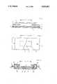
- FIG. 1is a cross-sectional elevation view, partially exploded, showing the construction of the flexible circuit manufactured in accordance with the present invention, prior to the formation of the through-hole contacts and the circuit pattern;
- FIG. 2is a plan view of the laminate shown in FIG. 1;
- FIG. 3is a cross-sectional elevation view of the circuit board manufactured in accordance with the invention, subsequent to through-hole forming and circuit pattern formation.
- the manufacturing process in accordance with the present inventionconsists, in the first step, of providing a means of alignment such as registration holes 4 to a flexible base material 3.
- Base material 3usually comprises a circuit laminate consisting of a conductive foil 7, preferably made of copper, a non-conductive carrier film 5 and an adhesive layer 6 sandwiched between conductive foil 7 and non-conductive carrier film 5.
- an adhesive layer 2is applied to the carrier film 5 of base material 3 with care to avoid the deposition of any adhesive 2 on the bending or flexing area "a".
- Adhesive layer 2may comprise an adhesive film or a non-flowing prepreg.
- the resulting space or region 9 in adhesive layer 2 on base material 3is determined with the aid of the alignment means, i.e., registration holes 4.
- an upper copper layer or foil 1is placed on the upper adhesive layer 2. This construction, as shown in FIG. 1, is now laminated under heat and pressure to form a flexible laminate unit.
- Contact through-holes 10are selectively formed at locations outside the bending or flexing region "a".
- the positions of through-holes 10, which are to be located outside the bending area "a", (and those of the circuit patterns which must be formed within the bending area "a” above the empty space 9),can be accurately determined with the aid of the registration holes 4 or other alignment means and formed via the use of conventional masking techniques.
- the conductive (copper) foil 1 that has been laminated on top of adhesive 2(and which has been provided with masks for the formation of conductive through-holes and circuit traces) is etched away in the bending area "a", at the same time that the circuit pattern is formed, so that carrier film 5 of base material 3 is exposed.
- an upper covering film 8 and a lower covering film 11are applied to the conducting areas 1 and 7, respectively via respective adhesive layers 12 and 13.
- upper covering film 8 and adhesive layers 12have the same total thickness as carrier film 5 and adhesive layer 6.
- the circuit paths of the dynamically stressed bending area "a"are located in the "neutral section", that is, in the area that is neutral with respect to the forces generated during bending; and the surface of the circuit board is protected by a covering film 8 or a carrier film 5, neither of which has any exposed adhesive layer.
- a covering film 8 or a carrier film 5neither of which has any exposed adhesive layer.
- the present inventionit is possible to manufacture, at reasonable cost, through-hole contacted flexible circuit boards which perform at least as well as the well known one-sided circuit boards, in terms of their bending characteristics; particularly when subjected to dynamic stresses.
- the present inventioncontains the additional features and advantages of (1) locating the circuit patterns in the "neutral section" "a"; (2) no exposed adhesive layers, and therefore less chance for contamination of the electronic component; and (3) symmetry of construction within the dynamically stressed bending area "a".
Landscapes
- Engineering & Computer Science (AREA)
- Manufacturing & Machinery (AREA)
- Microelectronics & Electronic Packaging (AREA)
- Production Of Multi-Layered Print Wiring Board (AREA)
- Structure Of Printed Boards (AREA)
- Coupling Device And Connection With Printed Circuit (AREA)
- Socks And Pantyhose (AREA)
- Particle Formation And Scattering Control In Inkjet Printers (AREA)
- Polyoxymethylene Polymers And Polymers With Carbon-To-Carbon Bonds (AREA)
- Laminated Bodies (AREA)
- Printing Elements For Providing Electric Connections Between Printed Circuits (AREA)
Abstract
Description
This invention relates to a process for the manufacture of through-hole contacted flexible circuit boards which are suited for high bending stresses and the circuit boards derived therefrom.
Flexible circuit elements are commonly used in electronic components that are subjected to high dynamic bending stresses, such as, for example, in disk storages and printers. These flexible circuit elements must have a smooth and extremely clean surface, in order to avoid disturbances of the electromechanical functions (of the disc drive or other electronic component) as the result of particles released from the flexible circuit board; particularly particles released from the adhesive materials used in manufacturing the flexible circuitry.
Circuit boards for high bending stresses which have two circuit layers with through-hole contacts located outside the bending area, are usually designed to be flexible on one side and to have carrier and covering films of equal thickness (symmetrical laminar construction). The base material used is a carrier film, made, for example, of polyimide, with copper-laminated on both sides thereof. Generally, the copper layer or foil is attached to the carrier film by means of an adhesive layer. The formation of through-hole contacts and a conductive pattern (on the copper foil) is accomplished in a conventional manner by a subtraction process (etching). As a result, in the bending area, the conducting paths (circuit pattern) are formed on only one side thereof, and the other side is completely etched away. The conductors are then provided with a protective covering film, of the same thickness as the carrier film.
Despite the apparent symmetrical construction of the above-described flexible circuits, the conducting paths thereon are not located in the transverse section of the laminate that remains "neutral" when subjected to bending stress, that is, the section that is neither subjected to tensile or compressive strains (the "neutral section"). In fact, the adhesive layer of the carrier film (which has been etched away) will produce an asymmetry, which acts to displace the neutral section into other transverse areas. In addition, as a result of the exposed adhesive, the circuit board is liable to accumulate dust and to be subjected to abrasion and thereby contaminate the electronic component.
Attempts have also been made in the manufacture of the above-described flexible circuits to make the carrier film of the base material only half as thick as the covering film on the printed circuit side.
Also, a covering film with the same thickness as the carrier film has been applied on the side of the carrier film that is etched away. While this particular construction has no exposed adhesive, unfortunately, it is still impossible to achieve a strict symmetry in the bending area, which is attributable to the existence of the two layers of adhesive on the carrier film. Furthermore, the total thickness of the construction in the bending area cannot be made thin enough, and consequently flexible enough, as is possible in the case of a one-sided circuit board.
The above-discussed and other problems and deficiencies of the prior art are overcome or alleviated by the through-hole contacted flexible circuit board for high bending stresses and method of manufacture thereof of the present invention. In accordance with the present invention, a process is provided wherein through-hole contacted flexible circuit boards for high bending stresses can be manufactured with a strictly symmetrical laminar construction in the bending area. In that area, the conducting paths (circuit pattern) are located in the "neutral section" described above. Significantly, there are no exposed layers of adhesive in the bending area which could act as a contaminant.
The above-discussed and other advantages of the present invention will be apparent to and understood by those skilled in the art from the following detailed description and drawings.
Referring now to the drawings, wherein like elements are numbered alike in the several FIGURES:
FIG. 1 is a cross-sectional elevation view, partially exploded, showing the construction of the flexible circuit manufactured in accordance with the present invention, prior to the formation of the through-hole contacts and the circuit pattern;
FIG. 2 is a plan view of the laminate shown in FIG. 1; and
FIG. 3 is a cross-sectional elevation view of the circuit board manufactured in accordance with the invention, subsequent to through-hole forming and circuit pattern formation.
The manufacturing process in accordance with the present invention consists, in the first step, of providing a means of alignment such asregistration holes 4 to aflexible base material 3.Base material 3 usually comprises a circuit laminate consisting of aconductive foil 7, preferably made of copper, anon-conductive carrier film 5 and an adhesive layer 6 sandwiched betweenconductive foil 7 andnon-conductive carrier film 5. In the next step, anadhesive layer 2 is applied to thecarrier film 5 ofbase material 3 with care to avoid the deposition of anyadhesive 2 on the bending or flexing area "a".Adhesive layer 2 may comprise an adhesive film or a non-flowing prepreg. The resulting space or region 9 inadhesive layer 2 onbase material 3 is determined with the aid of the alignment means, i.e.,registration holes 4. Subsequently, an upper copper layer or foil 1 is placed on the upperadhesive layer 2. This construction, as shown in FIG. 1, is now laminated under heat and pressure to form a flexible laminate unit.
The further processing of this laminate unit takes place in the following manner:
Contact through-holes 10 are selectively formed at locations outside the bending or flexing region "a". The positions of through-holes 10, which are to be located outside the bending area "a", (and those of the circuit patterns which must be formed within the bending area "a" above the empty space 9), can be accurately determined with the aid of theregistration holes 4 or other alignment means and formed via the use of conventional masking techniques. Next, the conductive (copper) foil 1 that has been laminated on top of adhesive 2 (and which has been provided with masks for the formation of conductive through-holes and circuit traces) is etched away in the bending area "a", at the same time that the circuit pattern is formed, so thatcarrier film 5 ofbase material 3 is exposed. Finally, an upper coveringfilm 8 and a lower covering film 11 are applied to the conductingareas 1 and 7, respectively via respectiveadhesive layers film 8 andadhesive layers 12 have the same total thickness ascarrier film 5 and adhesive layer 6.
As is shown in FIG. 3, after the manufacturing steps described hereinabove, the circuit paths of the dynamically stressed bending area "a" are located in the "neutral section", that is, in the area that is neutral with respect to the forces generated during bending; and the surface of the circuit board is protected by a coveringfilm 8 or acarrier film 5, neither of which has any exposed adhesive layer. Another important feature of the present invention is that the cross section of the circuit board is strictly symmetrical in its construction within the bending area "a".
In accordance with the present invention, it is possible to manufacture, at reasonable cost, through-hole contacted flexible circuit boards which perform at least as well as the well known one-sided circuit boards, in terms of their bending characteristics; particularly when subjected to dynamic stresses. Moreover, the present invention contains the additional features and advantages of (1) locating the circuit patterns in the "neutral section" "a"; (2) no exposed adhesive layers, and therefore less chance for contamination of the electronic component; and (3) symmetry of construction within the dynamically stressed bending area "a".
While the present invention has been discussed in terms of a two (2) layer flexible circuit, it will be appreciated that the process described herein can equally form a circuit having three (3) or more layers. For example, in the case of a three layer circuit, an additional adhesive layer and conductive foil would be laminated to bottom covering film 11 (FIG. 3). Importantly, as was discussed with regard toadhesive layer 2, a second space or region corresponding to space 9 in region "a" would have no adhesive applied thereto. Thus, following an etching or similar subtractive step, the conductive foil would be etched away from this second space or region along with the formation of a circuit pattern. As a result, a symmetrical three layer flexible circuit of the type described above would be formed.
While preferred embodiments have been shown and described, various modifications and substitutions may be made thereto without departing from the spirit and scope of the invention. Accordingly, it is to be understood that the present invention has been described by way of illustrations and not limitation.
Claims (20)
1. A method of manufacturing a flexible circuit element comprising the steps of:
forming a first flexible non-conductive carrier film;
forming a first conductive layer;
providing a first adhesive layer between said first carrier film and said first conductive layer;
laminating said first carrier film, first adhesive layer and first conductive layer to form a flexible base laminate;
selectively providing a second adhesive layer to portions of said first carrier film of said flexible base laminate whereby at least one area on said first carrier film has no adhesive and defines a bending region; and
providing a second conductive layer on said second adhesive layer whereby said bending region is covered by said second conductive layer and defines a space; and
laminating said flexible base laminate, second adhesive layer and second conductive layer to define a flexible laminate unit.
2. The method of claim 1 including the steps of:
forming at least one conductive through-hole in said flexible laminate unit in a location outside of said bending region; and
forming a circuit pattern in said second conductive layer, a portion of said circuit pattern being formed over said space.
3. The method of claim 2 including the step of:
removing the portion of said second conductive layer over said space to expose some of said first carrier film.
4. The method of claim 3 including the steps of:
providing a third adhesive layer to the unremoved second conductive layer; and
providing an upper non-conductive covering film on said third adhesive layer.
5. The method of claim 3 including the steps of:
providing a fourth adhesive layer to the first conductive layer; and
providing a lower non-conductive covering film on said fourth adhesive layer.
6. The method of claim 4 including the steps of:
providing a fourth adhesive layer to the first conductive layer; and
providing a lower non-conductive covering film on said fourth adhesive layer.
7. The method of claim 4 wherein:
said upper covering film and third adhesive layer have a total thickness about equal to the total thickness of said first carrier film and said first adhesive layer.
8. The method of claim 6 wherein:
said upper covering film and third adhesive layer have a total thickness about equal to the total thickness of said first carrier film and said first adhesive layer.
9. The method of claim 3 wherein:
said step of removing the portion of said second conductive layer over said space is simultaneous with said step of forming said circuit pattern.
10. The method of claim 3 wherein:
said step of removing the portion of said second conductive layer over said space is accomplished by etching.
11. A flexible circuit element formed in a method of manufacturing comprising the steps of:
forming a first flexible non-conductive carrier film;
forming a first conductive layer;
providing a first adhesive layer between said first carrier film and said first conductive layer;
laminating said first carrier film, first adhesive layer and first conductive layer to form a flexible base laminate;
selectively providing a second adhesive layer to portions of said first carrier film of said flexible base laminate whereby at least one area on said first carrier film has no adhesive and defines a bending region; and
providing a second conductive layer on said second adhesive layer whereby said bending region is covered by said second conductive layer and defines a space; and
laminating said flexible base laminate, second adhesive layer and second conductive layer to define a flexible laminate unit.
12. The circuit element of claim 11 including the steps of:
forming at least one conductive through-hole in said flexible laminate unit in a location outside of said bending region; and
forming a circuit pattern in said second conductive layer, a portion of said circuit pattern being formed over said space.
13. The circuit element of claim 12 including the step of:
removing the portion of said second conductive layer over said space to expose some of said first carrier film.
14. The circuit element of claim 13 including the steps of:
providing a third adhesive layer to the unremoved second conductive layer; and
providing an upper non-conductive covering film on said third adhesive layer.
15. The circuit element of claim 13 including the steps of:
providing a fourth adhesive layer to the first conductive layer; and
providing a lower non-conductive covering film on said fourth adhesive layer.
16. The circuit element of claim 14 including the steps of:
providing a fourth adhesive layer to the first conductive layer; and
providing a lower non-conductive covering film on said fourth adhesive layer.
17. The circuit element of claim 14 wherein:
said upper covering film and third adhesive layer have a total thickness about equal to the total thickness of said first carrier film and said first adhesive layer.
18. The circuit element of claim 16 wherein:
said upper covering film and third adhesive layer have a total thickness about equal to the total thickness of said first carrier film and said first adhesive layer.
19. The circuit element of claim 13 wherein:
said step of removing the portion of said second conductive layer over said space is simultaneous with said step of forming said circuit pattern.
20. The circuit element of claim 13 wherein:
said step of removing the portion of said second conductive layer over said space is accomplished by etching.
Applications Claiming Priority (2)
| Application Number | Priority Date | Filing Date | Title |
|---|---|---|---|
| DE3434672ADE3434672C2 (en) | 1984-09-21 | 1984-09-21 | Process for the production of flexible printed circuit boards for high bending stress |
| DE3434672 | 1984-09-21 |
Publications (1)
| Publication Number | Publication Date |
|---|---|
| US4626462Atrue US4626462A (en) | 1986-12-02 |
Family
ID=6245970
Family Applications (1)
| Application Number | Title | Priority Date | Filing Date |
|---|---|---|---|
| US06/775,916Expired - LifetimeUS4626462A (en) | 1984-09-21 | 1985-09-13 | Process for the manufacture of through-hole contacted flexible circuit boards for high bending stresses and the circuit boards made therefrom |
Country Status (7)
| Country | Link |
|---|---|
| US (1) | US4626462A (en) |
| EP (1) | EP0175045B1 (en) |
| JP (1) | JPS62111498A (en) |
| AT (1) | ATE59756T1 (en) |
| DE (2) | DE3434672C2 (en) |
| ES (1) | ES8607673A1 (en) |
| NO (1) | NO163390C (en) |
Cited By (47)
| Publication number | Priority date | Publication date | Assignee | Title |
|---|---|---|---|---|
| US4715928A (en)* | 1985-09-27 | 1987-12-29 | Hamby Bill L | Flexible printed circuits and methods of fabricating and forming plated thru-holes therein |
| US4766811A (en)* | 1985-11-08 | 1988-08-30 | M.A.N.-Roland Druckmaschinen Aktiengesellschaft | Apparatus for and method of protecting the circumferential surface of a printing cylinder and protective cylinder |
| US4800461A (en)* | 1987-11-02 | 1989-01-24 | Teledyne Industries, Inc. | Multilayer combined rigid and flex printed circuits |
| US4812213A (en)* | 1988-05-06 | 1989-03-14 | Rogers Corporation | Process for the manufacture of multi-layer circuits with dynamic flexing regions and the flexible circuits made therefrom |
| WO1989011114A1 (en)* | 1988-05-06 | 1989-11-16 | Rogers Corporation | Process for the manufacture of multi-layer circuits with dynamic flexing regions and the flexible circuits made therefrom |
| US4906803A (en)* | 1988-11-08 | 1990-03-06 | International Business Machines Corporation | Flexible supporting cable for an electronic device and method of making same |
| US4961806A (en)* | 1986-12-10 | 1990-10-09 | Sanders Associates, Inc. | Method of making a printed circuit |
| US5004639A (en)* | 1990-01-23 | 1991-04-02 | Sheldahl, Inc. | Rigid flex printed circuit configuration |
| US5097390A (en)* | 1986-12-10 | 1992-03-17 | Interflex Corporation | Printed circuit and fabrication of same |
| US5214571A (en)* | 1986-12-10 | 1993-05-25 | Miraco, Inc. | Multilayer printed circuit and associated multilayer material |
| US5250758A (en)* | 1991-05-21 | 1993-10-05 | Elf Technologies, Inc. | Methods and systems of preparing extended length flexible harnesses |
| US5288542A (en)* | 1992-07-14 | 1994-02-22 | International Business Machines Corporation | Composite for providing a rigid-flexible circuit board construction and method for fabrication thereof |
| US5384690A (en)* | 1993-07-27 | 1995-01-24 | International Business Machines Corporation | Flex laminate package for a parallel processor |
| US5445869A (en)* | 1993-01-21 | 1995-08-29 | Matsushita Electric Industrial Co., Ltd. | Composite flexible substrate |
| US5499444A (en)* | 1994-08-02 | 1996-03-19 | Coesen, Inc. | Method of manufacturing a rigid flex printed circuit board |
| US5998738A (en)* | 1996-08-30 | 1999-12-07 | Motorola Inc. | Electronic control module |
| US6267386B1 (en)* | 1998-06-23 | 2001-07-31 | Firma Carl Freudenberg | Ring seal |
| US6827906B1 (en) | 1997-10-15 | 2004-12-07 | Aclara Biosciences, Inc. | Continuous form microstructure assay array |
| US20060194001A1 (en)* | 2005-02-16 | 2006-08-31 | Citizen Electronics Co., Ltd. | Adhesive sheet for attaching an electronic part and an electronic device having such an electronic part |
| US20080307644A1 (en)* | 2007-06-12 | 2008-12-18 | Texas Instruments Incorporated | Metal plugged substrates with no adhesive between metal and polyimide |
| US7658196B2 (en) | 2005-02-24 | 2010-02-09 | Ethicon Endo-Surgery, Inc. | System and method for determining implanted device orientation |
| US7775215B2 (en) | 2005-02-24 | 2010-08-17 | Ethicon Endo-Surgery, Inc. | System and method for determining implanted device positioning and obtaining pressure data |
| US7775966B2 (en) | 2005-02-24 | 2010-08-17 | Ethicon Endo-Surgery, Inc. | Non-invasive pressure measurement in a fluid adjustable restrictive device |
| US7844342B2 (en) | 2008-02-07 | 2010-11-30 | Ethicon Endo-Surgery, Inc. | Powering implantable restriction systems using light |
| US7927270B2 (en) | 2005-02-24 | 2011-04-19 | Ethicon Endo-Surgery, Inc. | External mechanical pressure sensor for gastric band pressure measurements |
| US20110216514A1 (en)* | 2010-03-03 | 2011-09-08 | Mutual-Tek Industries Co., Ltd. | Combined multilayer circuit board having embedded components and manufacturing method of the same |
| US8016744B2 (en) | 2005-02-24 | 2011-09-13 | Ethicon Endo-Surgery, Inc. | External pressure-based gastric band adjustment system and method |
| US8016745B2 (en) | 2005-02-24 | 2011-09-13 | Ethicon Endo-Surgery, Inc. | Monitoring of a food intake restriction device |
| US8034065B2 (en) | 2008-02-26 | 2011-10-11 | Ethicon Endo-Surgery, Inc. | Controlling pressure in adjustable restriction devices |
| US8057492B2 (en) | 2008-02-12 | 2011-11-15 | Ethicon Endo-Surgery, Inc. | Automatically adjusting band system with MEMS pump |
| US8066629B2 (en) | 2005-02-24 | 2011-11-29 | Ethicon Endo-Surgery, Inc. | Apparatus for adjustment and sensing of gastric band pressure |
| US8100870B2 (en) | 2007-12-14 | 2012-01-24 | Ethicon Endo-Surgery, Inc. | Adjustable height gastric restriction devices and methods |
| US8114345B2 (en) | 2008-02-08 | 2012-02-14 | Ethicon Endo-Surgery, Inc. | System and method of sterilizing an implantable medical device |
| WO2012034152A1 (en) | 2010-09-17 | 2012-03-22 | At & S Austria Technologie & Systemtechnik Aktiengesellschaft | Method for producing a circuit board consisting of a plurality of circuit board areas and circuit board |
| US8142452B2 (en) | 2007-12-27 | 2012-03-27 | Ethicon Endo-Surgery, Inc. | Controlling pressure in adjustable restriction devices |
| US8152710B2 (en) | 2006-04-06 | 2012-04-10 | Ethicon Endo-Surgery, Inc. | Physiological parameter analysis for an implantable restriction device and a data logger |
| US8187163B2 (en) | 2007-12-10 | 2012-05-29 | Ethicon Endo-Surgery, Inc. | Methods for implanting a gastric restriction device |
| US8187162B2 (en) | 2008-03-06 | 2012-05-29 | Ethicon Endo-Surgery, Inc. | Reorientation port |
| US8192350B2 (en) | 2008-01-28 | 2012-06-05 | Ethicon Endo-Surgery, Inc. | Methods and devices for measuring impedance in a gastric restriction system |
| US8221439B2 (en) | 2008-02-07 | 2012-07-17 | Ethicon Endo-Surgery, Inc. | Powering implantable restriction systems using kinetic motion |
| US8233995B2 (en) | 2008-03-06 | 2012-07-31 | Ethicon Endo-Surgery, Inc. | System and method of aligning an implantable antenna |
| US8337389B2 (en) | 2008-01-28 | 2012-12-25 | Ethicon Endo-Surgery, Inc. | Methods and devices for diagnosing performance of a gastric restriction system |
| US8377079B2 (en) | 2007-12-27 | 2013-02-19 | Ethicon Endo-Surgery, Inc. | Constant force mechanisms for regulating restriction devices |
| US8591532B2 (en) | 2008-02-12 | 2013-11-26 | Ethicon Endo-Sugery, Inc. | Automatically adjusting band system |
| US8591395B2 (en) | 2008-01-28 | 2013-11-26 | Ethicon Endo-Surgery, Inc. | Gastric restriction device data handling devices and methods |
| US8870742B2 (en) | 2006-04-06 | 2014-10-28 | Ethicon Endo-Surgery, Inc. | GUI for an implantable restriction device and a data logger |
| US10548229B2 (en) | 2014-06-03 | 2020-01-28 | Conti Temic Microelectronic Gmbh | Method for producing a foil arrangement and corresponding foil arrangement |
Families Citing this family (5)
| Publication number | Priority date | Publication date | Assignee | Title |
|---|---|---|---|---|
| DE3905657A1 (en)* | 1989-02-24 | 1990-08-30 | Telefunken Electronic Gmbh | Flexible supporting film |
| FR2919781A1 (en)* | 2007-07-31 | 2009-02-06 | Beauce Realisations Et Etudes | METHOD OF MANUFACTURING A SEMI-FLEXIBLE PRINTED CIRCUIT, PLATE USED FOR SUCH A METHOD, PRINTED CIRCUIT AND ELECTRONIC DEVICE THEREFOR |
| JP5157366B2 (en)* | 2007-10-26 | 2013-03-06 | 東洋紡株式会社 | RFID media manufacturing method |
| DE102011100555A1 (en)* | 2011-01-25 | 2012-07-26 | Jörg R. Bauer | Method for manufacturing bendable and/or resilient substrate, involves adjusting material properties of conductive layer in deformation minimized layer region so as to bend substrate |
| DE102011014902B3 (en)* | 2011-03-23 | 2012-02-02 | Leonhard Kurz Stiftung & Co. Kg | Producing an antenna component with a three-dimensional antenna, comprises forming an electrical conductive layer made of an electrical conductive lacquer onto a thermoplastic carrier foil in an antenna area formed as antenna structure |
Citations (6)
| Publication number | Priority date | Publication date | Assignee | Title |
|---|---|---|---|---|
| US4103102A (en)* | 1976-07-01 | 1978-07-25 | Bell Telephone Laboratories, Incorporated | Reinforced flexible printed wiring board |
| US4141614A (en)* | 1976-06-14 | 1979-02-27 | Diamond Power Specialty Corporation | Electrical connecting means |
| US4311749A (en)* | 1977-09-06 | 1982-01-19 | Nippondenso Co., Ltd. | Flame-proof flexible printed circuit board |
| US4496794A (en)* | 1980-09-15 | 1985-01-29 | Ciba-Geigy Corporation | Flexible base materials, their preparation and their use for printed circuits |
| US4528064A (en)* | 1980-12-08 | 1985-07-09 | Sony Corporation | Method of making multilayer circuit board |
| US4562119A (en)* | 1980-09-15 | 1985-12-31 | Ciba-Geigy Corporation | Flexible, printed circuit |
Family Cites Families (3)
| Publication number | Priority date | Publication date | Assignee | Title |
|---|---|---|---|---|
| DE2657212C3 (en)* | 1976-12-17 | 1982-09-02 | Schoeller & Co Elektronik Gmbh, 3552 Wetter | Process for the production of rigid and flexible areas having printed circuit boards |
| DE2946726C2 (en)* | 1979-11-20 | 1982-05-19 | Ruwel-Werke Spezialfabrik für Leiterplatten GmbH, 4170 Geldern | Printed circuit board with rigid and flexible areas and process for their manufacture |
| DE3318717C1 (en)* | 1983-05-21 | 1984-05-30 | Grundig E.M.V. Elektro-Mechanische Versuchsanstalt Max Grundig & Co KG, 8510 Fürth | Process for manufacturing printed circuit boards with rigid and flexible areas |
- 1984
- 1984-09-21DEDE3434672Apatent/DE3434672C2/ennot_activeExpired
- 1985
- 1985-02-13ATAT85101532Tpatent/ATE59756T1/ennot_activeIP Right Cessation
- 1985-02-13EPEP85101532Apatent/EP0175045B1/ennot_activeExpired - Lifetime
- 1985-02-13DEDE8585101532Tpatent/DE3581027D1/ennot_activeExpired - Lifetime
- 1985-03-08NONO850930Apatent/NO163390C/enunknown
- 1985-03-20ESES541404Apatent/ES8607673A1/ennot_activeExpired
- 1985-09-13USUS06/775,916patent/US4626462A/ennot_activeExpired - Lifetime
- 1985-09-19JPJP60207696Apatent/JPS62111498A/enactiveGranted
Patent Citations (6)
| Publication number | Priority date | Publication date | Assignee | Title |
|---|---|---|---|---|
| US4141614A (en)* | 1976-06-14 | 1979-02-27 | Diamond Power Specialty Corporation | Electrical connecting means |
| US4103102A (en)* | 1976-07-01 | 1978-07-25 | Bell Telephone Laboratories, Incorporated | Reinforced flexible printed wiring board |
| US4311749A (en)* | 1977-09-06 | 1982-01-19 | Nippondenso Co., Ltd. | Flame-proof flexible printed circuit board |
| US4496794A (en)* | 1980-09-15 | 1985-01-29 | Ciba-Geigy Corporation | Flexible base materials, their preparation and their use for printed circuits |
| US4562119A (en)* | 1980-09-15 | 1985-12-31 | Ciba-Geigy Corporation | Flexible, printed circuit |
| US4528064A (en)* | 1980-12-08 | 1985-07-09 | Sony Corporation | Method of making multilayer circuit board |
Cited By (59)
| Publication number | Priority date | Publication date | Assignee | Title |
|---|---|---|---|---|
| US4715928A (en)* | 1985-09-27 | 1987-12-29 | Hamby Bill L | Flexible printed circuits and methods of fabricating and forming plated thru-holes therein |
| US4766811A (en)* | 1985-11-08 | 1988-08-30 | M.A.N.-Roland Druckmaschinen Aktiengesellschaft | Apparatus for and method of protecting the circumferential surface of a printing cylinder and protective cylinder |
| US5097390A (en)* | 1986-12-10 | 1992-03-17 | Interflex Corporation | Printed circuit and fabrication of same |
| US5214571A (en)* | 1986-12-10 | 1993-05-25 | Miraco, Inc. | Multilayer printed circuit and associated multilayer material |
| US4961806A (en)* | 1986-12-10 | 1990-10-09 | Sanders Associates, Inc. | Method of making a printed circuit |
| US4800461A (en)* | 1987-11-02 | 1989-01-24 | Teledyne Industries, Inc. | Multilayer combined rigid and flex printed circuits |
| US4812213A (en)* | 1988-05-06 | 1989-03-14 | Rogers Corporation | Process for the manufacture of multi-layer circuits with dynamic flexing regions and the flexible circuits made therefrom |
| US4945029A (en)* | 1988-05-06 | 1990-07-31 | Rogers Corporation | Process for the manufacture of multi-layer circuits with dynamic flexing regions and the flexible circuits made therefrom |
| WO1989010985A1 (en)* | 1988-05-06 | 1989-11-16 | Rogers Corporation | Process for the manufacture of multi-layer circuits with dynamic flexing regions and the flexible circuits made therefrom |
| GB2230650A (en)* | 1988-05-06 | 1990-10-24 | Rogers Corp | Process for the manufacture of multi-layer circuits with dynamic flexing regions and the flexible circuits made therefrom |
| GB2230903A (en)* | 1988-05-06 | 1990-10-31 | Rogers Corp | Process for the manufacture of multi-layer circuits with dynamic flexing regions and the flexible circuits made therefrom |
| WO1989011114A1 (en)* | 1988-05-06 | 1989-11-16 | Rogers Corporation | Process for the manufacture of multi-layer circuits with dynamic flexing regions and the flexible circuits made therefrom |
| GB2230903B (en)* | 1988-05-06 | 1992-07-01 | Rogers Corp | Process for the manufacture of multi-layer circuits with dynamic flexing regions and the flexible circuits made therefrom |
| GB2230650B (en)* | 1988-05-06 | 1992-05-13 | Rogers Corp | Process for the manufacture of multi-layer circuits with dynamic flexing regions and the flexible circuits made therefrom |
| US4906803A (en)* | 1988-11-08 | 1990-03-06 | International Business Machines Corporation | Flexible supporting cable for an electronic device and method of making same |
| US5004639A (en)* | 1990-01-23 | 1991-04-02 | Sheldahl, Inc. | Rigid flex printed circuit configuration |
| US5250758A (en)* | 1991-05-21 | 1993-10-05 | Elf Technologies, Inc. | Methods and systems of preparing extended length flexible harnesses |
| US5288542A (en)* | 1992-07-14 | 1994-02-22 | International Business Machines Corporation | Composite for providing a rigid-flexible circuit board construction and method for fabrication thereof |
| US5378306A (en)* | 1992-07-14 | 1995-01-03 | International Business Machines Corporation | Composite for providing a rigid-flexible circuit board construction and method for fabrication thereof |
| US5445869A (en)* | 1993-01-21 | 1995-08-29 | Matsushita Electric Industrial Co., Ltd. | Composite flexible substrate |
| US5384690A (en)* | 1993-07-27 | 1995-01-24 | International Business Machines Corporation | Flex laminate package for a parallel processor |
| US5499444A (en)* | 1994-08-02 | 1996-03-19 | Coesen, Inc. | Method of manufacturing a rigid flex printed circuit board |
| US5998738A (en)* | 1996-08-30 | 1999-12-07 | Motorola Inc. | Electronic control module |
| US6827906B1 (en) | 1997-10-15 | 2004-12-07 | Aclara Biosciences, Inc. | Continuous form microstructure assay array |
| US6267386B1 (en)* | 1998-06-23 | 2001-07-31 | Firma Carl Freudenberg | Ring seal |
| US20060194001A1 (en)* | 2005-02-16 | 2006-08-31 | Citizen Electronics Co., Ltd. | Adhesive sheet for attaching an electronic part and an electronic device having such an electronic part |
| US7593231B2 (en)* | 2005-02-16 | 2009-09-22 | Citizen Electronics Co., Ltd. | Adhesive sheet for attaching an electronic part and an electronic device having such an electronic part |
| US7658196B2 (en) | 2005-02-24 | 2010-02-09 | Ethicon Endo-Surgery, Inc. | System and method for determining implanted device orientation |
| US7775215B2 (en) | 2005-02-24 | 2010-08-17 | Ethicon Endo-Surgery, Inc. | System and method for determining implanted device positioning and obtaining pressure data |
| US7775966B2 (en) | 2005-02-24 | 2010-08-17 | Ethicon Endo-Surgery, Inc. | Non-invasive pressure measurement in a fluid adjustable restrictive device |
| US7927270B2 (en) | 2005-02-24 | 2011-04-19 | Ethicon Endo-Surgery, Inc. | External mechanical pressure sensor for gastric band pressure measurements |
| US8016744B2 (en) | 2005-02-24 | 2011-09-13 | Ethicon Endo-Surgery, Inc. | External pressure-based gastric band adjustment system and method |
| US8016745B2 (en) | 2005-02-24 | 2011-09-13 | Ethicon Endo-Surgery, Inc. | Monitoring of a food intake restriction device |
| US8066629B2 (en) | 2005-02-24 | 2011-11-29 | Ethicon Endo-Surgery, Inc. | Apparatus for adjustment and sensing of gastric band pressure |
| US8870742B2 (en) | 2006-04-06 | 2014-10-28 | Ethicon Endo-Surgery, Inc. | GUI for an implantable restriction device and a data logger |
| US8152710B2 (en) | 2006-04-06 | 2012-04-10 | Ethicon Endo-Surgery, Inc. | Physiological parameter analysis for an implantable restriction device and a data logger |
| US20080307644A1 (en)* | 2007-06-12 | 2008-12-18 | Texas Instruments Incorporated | Metal plugged substrates with no adhesive between metal and polyimide |
| US7918018B2 (en)* | 2007-06-12 | 2011-04-05 | Texas Instruments Incorporated | Method of fabricating a semiconductor device |
| US8187163B2 (en) | 2007-12-10 | 2012-05-29 | Ethicon Endo-Surgery, Inc. | Methods for implanting a gastric restriction device |
| US8100870B2 (en) | 2007-12-14 | 2012-01-24 | Ethicon Endo-Surgery, Inc. | Adjustable height gastric restriction devices and methods |
| US8142452B2 (en) | 2007-12-27 | 2012-03-27 | Ethicon Endo-Surgery, Inc. | Controlling pressure in adjustable restriction devices |
| US8377079B2 (en) | 2007-12-27 | 2013-02-19 | Ethicon Endo-Surgery, Inc. | Constant force mechanisms for regulating restriction devices |
| US8591395B2 (en) | 2008-01-28 | 2013-11-26 | Ethicon Endo-Surgery, Inc. | Gastric restriction device data handling devices and methods |
| US8337389B2 (en) | 2008-01-28 | 2012-12-25 | Ethicon Endo-Surgery, Inc. | Methods and devices for diagnosing performance of a gastric restriction system |
| US8192350B2 (en) | 2008-01-28 | 2012-06-05 | Ethicon Endo-Surgery, Inc. | Methods and devices for measuring impedance in a gastric restriction system |
| US8221439B2 (en) | 2008-02-07 | 2012-07-17 | Ethicon Endo-Surgery, Inc. | Powering implantable restriction systems using kinetic motion |
| US7844342B2 (en) | 2008-02-07 | 2010-11-30 | Ethicon Endo-Surgery, Inc. | Powering implantable restriction systems using light |
| US8114345B2 (en) | 2008-02-08 | 2012-02-14 | Ethicon Endo-Surgery, Inc. | System and method of sterilizing an implantable medical device |
| US8057492B2 (en) | 2008-02-12 | 2011-11-15 | Ethicon Endo-Surgery, Inc. | Automatically adjusting band system with MEMS pump |
| US8591532B2 (en) | 2008-02-12 | 2013-11-26 | Ethicon Endo-Sugery, Inc. | Automatically adjusting band system |
| US8034065B2 (en) | 2008-02-26 | 2011-10-11 | Ethicon Endo-Surgery, Inc. | Controlling pressure in adjustable restriction devices |
| US8233995B2 (en) | 2008-03-06 | 2012-07-31 | Ethicon Endo-Surgery, Inc. | System and method of aligning an implantable antenna |
| US8187162B2 (en) | 2008-03-06 | 2012-05-29 | Ethicon Endo-Surgery, Inc. | Reorientation port |
| US20110216514A1 (en)* | 2010-03-03 | 2011-09-08 | Mutual-Tek Industries Co., Ltd. | Combined multilayer circuit board having embedded components and manufacturing method of the same |
| AT12737U1 (en)* | 2010-09-17 | 2012-10-15 | Austria Tech & System Tech | METHOD FOR PRODUCING A CONDUCTOR PLATE COMPOSED OF MULTIPLE PCB SURFACES AND PCB |
| WO2012034152A1 (en) | 2010-09-17 | 2012-03-22 | At & S Austria Technologie & Systemtechnik Aktiengesellschaft | Method for producing a circuit board consisting of a plurality of circuit board areas and circuit board |
| US9226390B2 (en) | 2010-09-17 | 2015-12-29 | At & S Austria Technologie & Systemtechnik Aktiengesellschaft | Method for producing a circuit board consisting of a plurality of circuit board areas and circuit board |
| US10321558B2 (en) | 2010-09-17 | 2019-06-11 | At & S Austria Technologie & Systemtechnik Aktiengesellschaft | Printed circuit board |
| US10548229B2 (en) | 2014-06-03 | 2020-01-28 | Conti Temic Microelectronic Gmbh | Method for producing a foil arrangement and corresponding foil arrangement |
Also Published As
| Publication number | Publication date |
|---|---|
| ATE59756T1 (en) | 1991-01-15 |
| ES541404A0 (en) | 1986-05-16 |
| JPS62111498A (en) | 1987-05-22 |
| NO163390C (en) | 1990-05-16 |
| EP0175045A2 (en) | 1986-03-26 |
| EP0175045A3 (en) | 1988-01-07 |
| NO850930L (en) | 1986-03-24 |
| DE3434672C2 (en) | 1986-09-11 |
| EP0175045B1 (en) | 1991-01-02 |
| DE3434672A1 (en) | 1986-03-27 |
| NO163390B (en) | 1990-02-05 |
| JPH0141277B2 (en) | 1989-09-04 |
| ES8607673A1 (en) | 1986-05-16 |
| DE3581027D1 (en) | 1991-02-07 |
Similar Documents
| Publication | Publication Date | Title |
|---|---|---|
| US4626462A (en) | Process for the manufacture of through-hole contacted flexible circuit boards for high bending stresses and the circuit boards made therefrom | |
| US7152314B2 (en) | Method of manufacturing circuit board | |
| US7663225B2 (en) | Method for manufacturing electronic components, mother substrate, and electronic component | |
| JPH04212494A (en) | Manufacture of rigid/flexible printed circuit structure and multilayer flexible circuit board manufactured by this method | |
| US4945029A (en) | Process for the manufacture of multi-layer circuits with dynamic flexing regions and the flexible circuits made therefrom | |
| US4812213A (en) | Process for the manufacture of multi-layer circuits with dynamic flexing regions and the flexible circuits made therefrom | |
| US6198052B1 (en) | Circuit board with terminal accommodating level differences | |
| JPH08125342A (en) | Flexible multilayered wiring board and its manufacture | |
| JP3895697B2 (en) | Flexible printed circuit board | |
| WO1993011652A1 (en) | Printed circuit combination and process | |
| KR20070045787A (en) | Manufacturing method of flexible printed circuit board | |
| KR20020050720A (en) | Processes for manufacturing multilayer flexible wiring boards | |
| JP3871910B2 (en) | Flexible printed circuit board having cable and manufacturing method thereof | |
| JP3740711B2 (en) | Multilayer printed wiring board | |
| KR20060066971A (en) | Manufacturing method of double sided flexible circuit board | |
| JP2740028B2 (en) | Multilayer printed wiring board | |
| JP3227828B2 (en) | Connection method between multilayer thin film device and thin film | |
| JPH0974252A (en) | Flex rigid printed wiring board and manufacturing method thereof | |
| KR102551217B1 (en) | Carrier substrate and printed circuit board fabricated using the same | |
| JP3237416B2 (en) | Inner layer circuit board and multilayer printed copper-clad laminate using the inner layer circuit board | |
| JPH05183272A (en) | Manufacture of multilayer board for mounting electronic parts | |
| JP4473847B2 (en) | Flexible printed circuit board and manufacturing method thereof | |
| JPH0226399B2 (en) | ||
| JPH04349693A (en) | Method of throughhole working in printed wiring board | |
| JPH04261096A (en) | Multilayer printed board and manufacture |
Legal Events
| Date | Code | Title | Description |
|---|---|---|---|
| AS | Assignment | Owner name:CARL FREUDENBERG, 6940 WEILHEM, WEST GERMANY Free format text:ASSIGNMENT OF ASSIGNORS INTEREST.;ASSIGNORS:KOBER, HORST;TROGISCH, GUNTER;REEL/FRAME:004535/0341 Effective date:19851115 | |
| STCF | Information on status: patent grant | Free format text:PATENTED CASE | |
| FEPP | Fee payment procedure | Free format text:PAYOR NUMBER ASSIGNED (ORIGINAL EVENT CODE: ASPN); ENTITY STATUS OF PATENT OWNER: LARGE ENTITY | |
| FPAY | Fee payment | Year of fee payment:4 | |
| FEPP | Fee payment procedure | Free format text:PAYER NUMBER DE-ASSIGNED (ORIGINAL EVENT CODE: RMPN); ENTITY STATUS OF PATENT OWNER: LARGE ENTITY Free format text:PAYOR NUMBER ASSIGNED (ORIGINAL EVENT CODE: ASPN); ENTITY STATUS OF PATENT OWNER: LARGE ENTITY | |
| FPAY | Fee payment | Year of fee payment:8 | |
| REMI | Maintenance fee reminder mailed | ||
| FPAY | Fee payment | Year of fee payment:12 |