US4619680A - Manufacture of integrated optical waveguides - Google Patents
Manufacture of integrated optical waveguidesDownload PDFInfo
- Publication number
- US4619680A US4619680AUS06/742,207US74220785AUS4619680AUS 4619680 AUS4619680 AUS 4619680AUS 74220785 AUS74220785 AUS 74220785AUS 4619680 AUS4619680 AUS 4619680A
- Authority
- US
- United States
- Prior art keywords
- substrate
- layer
- glass
- tube
- reaction tube
- Prior art date
- Legal status (The legal status is an assumption and is not a legal conclusion. Google has not performed a legal analysis and makes no representation as to the accuracy of the status listed.)
- Expired - Lifetime
Links
Images

Classifications
- G—PHYSICS
- G02—OPTICS
- G02B—OPTICAL ELEMENTS, SYSTEMS OR APPARATUS
- G02B6/00—Light guides; Structural details of arrangements comprising light guides and other optical elements, e.g. couplings
- G02B6/10—Light guides; Structural details of arrangements comprising light guides and other optical elements, e.g. couplings of the optical waveguide type
- G02B6/12—Light guides; Structural details of arrangements comprising light guides and other optical elements, e.g. couplings of the optical waveguide type of the integrated circuit kind
- G02B6/13—Integrated optical circuits characterised by the manufacturing method
- G02B6/132—Integrated optical circuits characterised by the manufacturing method by deposition of thin films
- C—CHEMISTRY; METALLURGY
- C03—GLASS; MINERAL OR SLAG WOOL
- C03C—CHEMICAL COMPOSITION OF GLASSES, GLAZES OR VITREOUS ENAMELS; SURFACE TREATMENT OF GLASS; SURFACE TREATMENT OF FIBRES OR FILAMENTS MADE FROM GLASS, MINERALS OR SLAGS; JOINING GLASS TO GLASS OR OTHER MATERIALS
- C03C17/00—Surface treatment of glass, not in the form of fibres or filaments, by coating
- C03C17/02—Surface treatment of glass, not in the form of fibres or filaments, by coating with glass
Definitions
- This inventionrelates to the manufacture of integrated optical waveguides.
- Integrated optical waveguidesare waveguides which are integral with a generally planar substrate and in which, either the waveguide is uniform across the plane of the substrate-planar waveguides, or the waveguide consists of stripes of guiding material on the substrate provided in patterns-stripe waveguides.
- Conventionally such waveguideshave been manufactured by depositing the waveguide material--usually glass which has been doped to adjust its refractive index, by deposition of glass particles on the surface of the substrate and then heating to fuse the waveguide. This process however requires very careful temperature control since no glass particles are deposited without a temperature gradient along the direction of flow of the gas incorporating the reactants.
- the inventionprovides, according to one aspect, a method of manufacturing integrated optical waveguides wherein the waveguide is composed of glass deposited in a first layer on a substrate by plasma chemical vapour deposition.
- a second layer of a lower refractive index glassis deposited over said first layer.
- the said first layer of glassis shaped to a desired pattern on the substrate and said second layer of glass is deposited over said desired pattern of glass.
- the desired pattern of glassmay be formed by selective removal of part of the first layer after deposition so as to leave the desired pattern, the removal conveniently being achieved by masking the first layer with the desired pattern and then etching away the remainder of the first layer of glass.
- the desired patternmay be achieved by producing grooves in the desired pattern in the substrate and then depositing the first layer so that the desired pattern is formed at the bottom of the pattern of grooves. In this way removal of the rest of the first layer is not required and the second layer of glass can be immediately deposited over the first layer.
- the second layer of glassis also deposited by plasma chemical vapour deposition.
- the substrateis preferably formed of the same glass as that used for the second layer so that the first layer, forming a core, is embedded within a cladding of lower refractive index glass.
- the method according to the inventionthus allows the manufacture of large number of planar or striped waveguides forming passive or active integrated optical devices such as beam splitters/combiners, directional couplers or wavelength multiplexers/demultiplexers.
- FIG. 1is a schematic diagram of apparatus used for manufacturing integrated optical waveguides according to the invention
- FIGS. 2(a), 2(b), 2(c) and 2(d)show diagrammatically the steps taken in one method according to the invention.
- FIGS. 3(a), 3(b), 3(c) and 3(d)show diagrammatically the steps taken in a second method according to the invention.
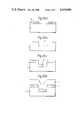
- the desired waveguide patternis first written on a substrate 11 using photolithography.
- the substrateis made of a glass having the same index of refraction as that which is to be used to form the cladding layer.
- the rest of the substrateis then covered with a mask 12 made of a suitable material (FIG. 2(a)) and the pattern etched using any known process e.g. chemically or by ion sputtering.
- the mask 12is then removed leaving the substrate covered by a pattern of grooves 13 (FIG. 2(b)) in which the waveguides will be embedded.
- the core glass 14is then deposited on the substrate by plasma chemical vapour deposition as will be described further below with reference to FIG. 1.
- the core glass 14 constituting the waveguidehas an index of refraction slightly higher than that of the cladding layer 15 and the substrate 11 and, by suitably controlling the amount of dopant in the core glass as the deposition process is carried out, it may have any desired refractive-index profile across its thickness which is less than the depth of the grooves 13 so that the waveguide 14 is fully embedded within the grooves 13 (FIG. 2(c)).
- the cladding layer 15is then deposited, again by plasma chemical vapour deposition, over the core glass 14 to form the completed integrated optical waveguide (FIG. 2(d)).
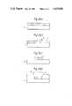
- FIG. 3An alternative method of manufacturing integrated optical waveguides is shown in FIG. 3 in which the core material 14 is first deposited by plasma chemical vapour deposition in the form of a planar layer with the required refractive-index profile (FIG. 3(a)). The required waveguide pattern is then written photolithographically on the deposited core layer and this pattern is suitably masked 12 (FIG. 3(b)). The rest of the deposited core layer is completely etched away, either chemically or by ion sputtering or in any other way, and the mask 12 is removed (FIG. 3(c)). Finally the cladding layer 15 is deposited to form the completed integrated optical waveguide (FIG. 3(d)).
- the apparatus shown in FIG. 1may be used. It consists of a silica tube 1 which has been shaped to provide a shoulder 2 on which a second, shorter silica tube 3 with a smaller diameter is coaxially positioned.
- the first silica tube 1is closed at one end, through which a third, perforated silica tube 4 extends into the second, inner tube 3, and is connected at its other end to a vacuum pump (not shown).
- the perforated silica tube 4extends coaxially through the inner tube 3 and is perforated throughout the region surrounded by the inner tube 3. It is closed off at its end within the first tube 1 so that gases which are fed into the perforated tube 4 (as indicated by the arrow) must flow through the perforations 5 before being sucked out by the pump.
- the gasesflow through the perforations 5, they enter a reaction zone in the inner silica tube 3 where a chemical reaction is initiated by means of a plasma produced in the reaction zone by a microwave cavity 6 positioned below the reaction zone and supplied with power from a microwave generator (not shown).
- the gasesusually consist of oxygen plus the vapours of one or more halides as well as an easily ionizable gas such as argon.
- the chemical reactionproduces glass doped with various dopants as required which is deposited on the substrate 7 mounted within a window 8 cut into the inner silica tube 3 and thus exposed to the reaction zone within the tube 3.
- the pressure in the reaction zoneis maintained at around 10 Torr and the microwave power and relative flow rates of the gases and vapours are adjusted to produce a plasma column of the desired length.
- a heating coil 9is positioned along the length of the reaction zone on the outside of the silica tube 1 to maintain the substrates at a suitable temperature.
- the temperaturedoes not directly affect the chemical reactions or the deposition rates but is necessary in order that a good thermal match is achieved between the substrate and the deposited layers. Failure to maintain a sufficiently high temperature in the reaction zone could cause the deposited layers to be cracked and/or not adhere to the substrate.
- a temperature of around 1000° C.is often needed to achieve a good thermal match between the deposited layers and the substrates, however when only thin layers are to be deposited, lower temperatures could be used.
- Both the flow rate and the composition of the gaseous mixture flowing through tubes 4 and 3can be modified (either manually or under computer control) during the deposition time. This allows the composition of the deposited layer, and in particular its refractive index, to be modified so that the desired infractive index profile can be obtained.
- Plasma chemical vapour depositionis particularly useful for depositing glass doped with GeO 2 so that its photorefractive properties can be utilised for integrated optical devices.
Landscapes
- Engineering & Computer Science (AREA)
- Chemical & Material Sciences (AREA)
- Physics & Mathematics (AREA)
- General Physics & Mathematics (AREA)
- Optics & Photonics (AREA)
- Life Sciences & Earth Sciences (AREA)
- Microelectronics & Electronic Packaging (AREA)
- Chemical Kinetics & Catalysis (AREA)
- General Chemical & Material Sciences (AREA)
- Geochemistry & Mineralogy (AREA)
- Materials Engineering (AREA)
- Organic Chemistry (AREA)
- Optical Integrated Circuits (AREA)
- Manufacture, Treatment Of Glass Fibers (AREA)
Abstract
Description
Claims (12)
Applications Claiming Priority (2)
| Application Number | Priority Date | Filing Date | Title |
|---|---|---|---|
| GB8414878 | 1984-06-11 | ||
| GB848414878AGB8414878D0 (en) | 1984-06-11 | 1984-06-11 | Integrated optical waveguides |
Publications (1)
| Publication Number | Publication Date |
|---|---|
| US4619680Atrue US4619680A (en) | 1986-10-28 |
Family
ID=10562260
Family Applications (1)
| Application Number | Title | Priority Date | Filing Date |
|---|---|---|---|
| US06/742,207Expired - LifetimeUS4619680A (en) | 1984-06-11 | 1985-06-07 | Manufacture of integrated optical waveguides |
Country Status (4)
| Country | Link |
|---|---|
| US (1) | US4619680A (en) |
| DE (1) | DE3520813C2 (en) |
| FR (1) | FR2565701B1 (en) |
| GB (2) | GB8414878D0 (en) |
Cited By (46)
| Publication number | Priority date | Publication date | Assignee | Title |
|---|---|---|---|---|
| US5613995A (en)* | 1993-04-23 | 1997-03-25 | Lucent Technologies Inc. | Method for making planar optical waveguides |
| US6138478A (en)* | 1992-09-21 | 2000-10-31 | Ceramoptec Industries, Inc. | Method of forming an optical fiber preform using an E020 plasma field configuration |
| US6377732B1 (en)* | 1999-01-22 | 2002-04-23 | The Whitaker Corporation | Planar waveguide devices and fiber attachment |
| US20030110808A1 (en)* | 2001-12-14 | 2003-06-19 | Applied Materials Inc., A Delaware Corporation | Method of manufacturing an optical core |
| US20030113085A1 (en)* | 2001-12-14 | 2003-06-19 | Applied Materials, Inc., A Delaware Corporation | HDP-CVD film for uppercladding application in optical waveguides |
| US20030117691A1 (en)* | 2001-12-21 | 2003-06-26 | Xiangxin Bi | Three dimensional engineering of planar optical structures |
| US20030232200A1 (en)* | 2000-10-26 | 2003-12-18 | Bryan Michael A. | Multilayered optical structures |
| US20040079118A1 (en)* | 2002-10-23 | 2004-04-29 | Applied Materials Inc | Method of forming a phosphorus doped optical core using a PECVD process |
| US20040237593A1 (en)* | 2001-10-01 | 2004-12-02 | Van Stralen Mattheus Jacobus Nicolaas | Method and device for depositing glass layers on the external surface of a rod-like glass preform |
| US20050115921A1 (en)* | 2000-12-11 | 2005-06-02 | Mak Cecilia Y. | Optical integrated circuits (ics) |
| US20050199013A1 (en)* | 2004-03-12 | 2005-09-15 | Applied Materials, Inc. | Use of amorphous carbon film as a hardmask in the fabrication of optical waveguides |
| US7000434B2 (en)* | 2000-12-19 | 2006-02-21 | Intel Corporation | Method of creating an angled waveguide using lithographic techniques |
| US20060088267A1 (en)* | 2004-10-21 | 2006-04-27 | Sumitomo Electric Industries, Ltd. | Production method of optical waveguide device and optical waveguide device |
| CN1303444C (en)* | 2001-03-16 | 2007-03-07 | 奥普托内斯特公司 | Method of manufacturing planar optical waveguide circuit and planar optical waveguide circuit |
| US7205662B2 (en) | 2003-02-27 | 2007-04-17 | Symmorphix, Inc. | Dielectric barrier layer films |
| US7238628B2 (en) | 2003-05-23 | 2007-07-03 | Symmorphix, Inc. | Energy conversion and storage films and devices by physical vapor deposition of titanium and titanium oxides and sub-oxides |
| US7290407B1 (en)* | 2001-12-19 | 2007-11-06 | Jesse Chienhua Shan | Triangle-shaped planar optical waveguide having reduced scattering loss |
| US7378356B2 (en) | 2002-03-16 | 2008-05-27 | Springworks, Llc | Biased pulse DC reactive sputtering of oxide films |
| US7404877B2 (en) | 2001-11-09 | 2008-07-29 | Springworks, Llc | Low temperature zirconia based thermal barrier layer by PVD |
| US7469558B2 (en)* | 2001-07-10 | 2008-12-30 | Springworks, Llc | As-deposited planar optical waveguides with low scattering loss and methods for their manufacture |
| US7826702B2 (en) | 2002-08-27 | 2010-11-02 | Springworks, Llc | Optically coupling into highly uniform waveguides |
| US7838133B2 (en) | 2005-09-02 | 2010-11-23 | Springworks, Llc | Deposition of perovskite and other compound ceramic films for dielectric applications |
| US7959769B2 (en) | 2004-12-08 | 2011-06-14 | Infinite Power Solutions, Inc. | Deposition of LiCoO2 |
| US7993773B2 (en) | 2002-08-09 | 2011-08-09 | Infinite Power Solutions, Inc. | Electrochemical apparatus with barrier layer protected substrate |
| US8021778B2 (en) | 2002-08-09 | 2011-09-20 | Infinite Power Solutions, Inc. | Electrochemical apparatus with barrier layer protected substrate |
| US8045832B2 (en) | 2002-03-16 | 2011-10-25 | Springworks, Llc | Mode size converter for a planar waveguide |
| US8062708B2 (en) | 2006-09-29 | 2011-11-22 | Infinite Power Solutions, Inc. | Masking of and material constraint for depositing battery layers on flexible substrates |
| US8197781B2 (en) | 2006-11-07 | 2012-06-12 | Infinite Power Solutions, Inc. | Sputtering target of Li3PO4 and method for producing same |
| US8236443B2 (en) | 2002-08-09 | 2012-08-07 | Infinite Power Solutions, Inc. | Metal film encapsulation |
| US8260203B2 (en) | 2008-09-12 | 2012-09-04 | Infinite Power Solutions, Inc. | Energy device with integral conductive surface for data communication via electromagnetic energy and method thereof |
| US8268488B2 (en) | 2007-12-21 | 2012-09-18 | Infinite Power Solutions, Inc. | Thin film electrolyte for thin film batteries |
| US8350519B2 (en) | 2008-04-02 | 2013-01-08 | Infinite Power Solutions, Inc | Passive over/under voltage control and protection for energy storage devices associated with energy harvesting |
| US8394522B2 (en) | 2002-08-09 | 2013-03-12 | Infinite Power Solutions, Inc. | Robust metal film encapsulation |
| US8404376B2 (en) | 2002-08-09 | 2013-03-26 | Infinite Power Solutions, Inc. | Metal film encapsulation |
| US8431264B2 (en) | 2002-08-09 | 2013-04-30 | Infinite Power Solutions, Inc. | Hybrid thin-film battery |
| US8445130B2 (en) | 2002-08-09 | 2013-05-21 | Infinite Power Solutions, Inc. | Hybrid thin-film battery |
| US8508193B2 (en) | 2008-10-08 | 2013-08-13 | Infinite Power Solutions, Inc. | Environmentally-powered wireless sensor module |
| US8518581B2 (en) | 2008-01-11 | 2013-08-27 | Inifinite Power Solutions, Inc. | Thin film encapsulation for thin film batteries and other devices |
| US8599572B2 (en) | 2009-09-01 | 2013-12-03 | Infinite Power Solutions, Inc. | Printed circuit board with integrated thin film battery |
| US8636876B2 (en) | 2004-12-08 | 2014-01-28 | R. Ernest Demaray | Deposition of LiCoO2 |
| US8728285B2 (en) | 2003-05-23 | 2014-05-20 | Demaray, Llc | Transparent conductive oxides |
| US8906523B2 (en) | 2008-08-11 | 2014-12-09 | Infinite Power Solutions, Inc. | Energy device with integral collector surface for electromagnetic energy harvesting and method thereof |
| US9018108B2 (en) | 2013-01-25 | 2015-04-28 | Applied Materials, Inc. | Low shrinkage dielectric films |
| US9334557B2 (en) | 2007-12-21 | 2016-05-10 | Sapurast Research Llc | Method for sputter targets for electrolyte films |
| US9634296B2 (en) | 2002-08-09 | 2017-04-25 | Sapurast Research Llc | Thin film battery on an integrated circuit or circuit board and method thereof |
| US10680277B2 (en) | 2010-06-07 | 2020-06-09 | Sapurast Research Llc | Rechargeable, high-density electrochemical device |
Families Citing this family (2)
| Publication number | Priority date | Publication date | Assignee | Title |
|---|---|---|---|---|
| DE3619379A1 (en)* | 1986-06-09 | 1986-12-18 | Martin Prof. Dr.-Ing. 4630 Bochum Fiebig | Method and devices for producing optical glass objects |
| GB8620273D0 (en)* | 1986-08-20 | 1986-10-01 | Gen Electric Co Plc | Deposition of thin films |
Citations (9)
| Publication number | Priority date | Publication date | Assignee | Title |
|---|---|---|---|---|
| US3934061A (en)* | 1972-03-30 | 1976-01-20 | Corning Glass Works | Method of forming planar optical waveguides |
| JPS5781213A (en)* | 1980-11-11 | 1982-05-21 | Nippon Telegr & Teleph Corp <Ntt> | Production of thin film for optical waveguide |
| US4341541A (en)* | 1979-07-13 | 1982-07-27 | Times Fiber Communications, Inc. | Process for the production of optical fiber |
| US4345928A (en)* | 1979-10-09 | 1982-08-24 | Nippon Telegraph & Telephone Public Corporation | Fabrication method of single-mode optical fiber preforms |
| US4367085A (en)* | 1980-01-07 | 1983-01-04 | Nippon Telegraph & Telephone Public Corporation | Method of fabricating multi-mode optical fiber preforms |
| JPS58100801A (en)* | 1981-12-12 | 1983-06-15 | Nippon Telegr & Teleph Corp <Ntt> | Production of quartz optical waveguide |
| US4425146A (en)* | 1979-12-17 | 1984-01-10 | Nippon Telegraph & Telephone Public Corporation | Method of making glass waveguide for optical circuit |
| GB2134099A (en)* | 1983-01-24 | 1984-08-08 | Ass Elect Ind | Tube manufacture |
| US4494968A (en)* | 1983-10-03 | 1985-01-22 | Corning Glass Works | Method of forming laminated single polarization fiber |
Family Cites Families (9)
| Publication number | Priority date | Publication date | Assignee | Title |
|---|---|---|---|---|
| DE2444100C3 (en)* | 1974-09-14 | 1979-04-12 | Philips Patentverwaltung Gmbh, 2000 Hamburg | Process for the production of internally coated glass tubes for drawing optical fibers |
| US4196232A (en)* | 1975-12-18 | 1980-04-01 | Rca Corporation | Method of chemically vapor-depositing a low-stress glass layer |
| DE2642949C3 (en)* | 1976-09-24 | 1980-11-20 | Philips Patentverwaltung Gmbh, 2000 Hamburg | Process for the production of internally coated glass tubes for drawing optical fibers |
| GB1559978A (en)* | 1976-12-01 | 1980-01-30 | Gen Electric Co Ltd | Chemical vapour deposition processes |
| US4328646A (en)* | 1978-11-27 | 1982-05-11 | Rca Corporation | Method for preparing an abrasive coating |
| US4268711A (en)* | 1979-04-26 | 1981-05-19 | Optical Coating Laboratory, Inc. | Method and apparatus for forming films from vapors using a contained plasma source |
| DE3015880A1 (en)* | 1980-04-24 | 1981-10-29 | Siemens AG, 1000 Berlin und 8000 München | METHOD FOR PRODUCING AN OPTICAL DEVICE USING A FOCUS |
| JPS57104106A (en)* | 1980-12-22 | 1982-06-29 | Nippon Sheet Glass Co Ltd | Production of optical circuit |
| JPS592008A (en)* | 1982-06-28 | 1984-01-07 | Nippon Telegr & Teleph Corp <Ntt> | Production of embedding type quartz optical waveguide |
- 1984
- 1984-06-11GBGB848414878Apatent/GB8414878D0/enactivePending
- 1985
- 1985-06-07USUS06/742,207patent/US4619680A/ennot_activeExpired - Lifetime
- 1985-06-10GBGB08514618Apatent/GB2160226B/ennot_activeExpired
- 1985-06-10FRFR858508749Apatent/FR2565701B1/ennot_activeExpired - Lifetime
- 1985-06-11DEDE3520813Apatent/DE3520813C2/ennot_activeExpired - Fee Related
Patent Citations (9)
| Publication number | Priority date | Publication date | Assignee | Title |
|---|---|---|---|---|
| US3934061A (en)* | 1972-03-30 | 1976-01-20 | Corning Glass Works | Method of forming planar optical waveguides |
| US4341541A (en)* | 1979-07-13 | 1982-07-27 | Times Fiber Communications, Inc. | Process for the production of optical fiber |
| US4345928A (en)* | 1979-10-09 | 1982-08-24 | Nippon Telegraph & Telephone Public Corporation | Fabrication method of single-mode optical fiber preforms |
| US4425146A (en)* | 1979-12-17 | 1984-01-10 | Nippon Telegraph & Telephone Public Corporation | Method of making glass waveguide for optical circuit |
| US4367085A (en)* | 1980-01-07 | 1983-01-04 | Nippon Telegraph & Telephone Public Corporation | Method of fabricating multi-mode optical fiber preforms |
| JPS5781213A (en)* | 1980-11-11 | 1982-05-21 | Nippon Telegr & Teleph Corp <Ntt> | Production of thin film for optical waveguide |
| JPS58100801A (en)* | 1981-12-12 | 1983-06-15 | Nippon Telegr & Teleph Corp <Ntt> | Production of quartz optical waveguide |
| GB2134099A (en)* | 1983-01-24 | 1984-08-08 | Ass Elect Ind | Tube manufacture |
| US4494968A (en)* | 1983-10-03 | 1985-01-22 | Corning Glass Works | Method of forming laminated single polarization fiber |
Cited By (68)
| Publication number | Priority date | Publication date | Assignee | Title |
|---|---|---|---|---|
| US6138478A (en)* | 1992-09-21 | 2000-10-31 | Ceramoptec Industries, Inc. | Method of forming an optical fiber preform using an E020 plasma field configuration |
| US5613995A (en)* | 1993-04-23 | 1997-03-25 | Lucent Technologies Inc. | Method for making planar optical waveguides |
| US6377732B1 (en)* | 1999-01-22 | 2002-04-23 | The Whitaker Corporation | Planar waveguide devices and fiber attachment |
| US7039264B2 (en) | 2000-10-26 | 2006-05-02 | Neophotonics Corporation | Multilayered optical structures |
| US20030232200A1 (en)* | 2000-10-26 | 2003-12-18 | Bryan Michael A. | Multilayered optical structures |
| US9939579B2 (en) | 2000-10-26 | 2018-04-10 | Neophotonics Corporation | Multilayered optical structures |
| US7087179B2 (en) | 2000-12-11 | 2006-08-08 | Applied Materials, Inc. | Optical integrated circuits (ICs) |
| US20050115921A1 (en)* | 2000-12-11 | 2005-06-02 | Mak Cecilia Y. | Optical integrated circuits (ics) |
| US7000434B2 (en)* | 2000-12-19 | 2006-02-21 | Intel Corporation | Method of creating an angled waveguide using lithographic techniques |
| CN1303444C (en)* | 2001-03-16 | 2007-03-07 | 奥普托内斯特公司 | Method of manufacturing planar optical waveguide circuit and planar optical waveguide circuit |
| US7469558B2 (en)* | 2001-07-10 | 2008-12-30 | Springworks, Llc | As-deposited planar optical waveguides with low scattering loss and methods for their manufacture |
| US20040237593A1 (en)* | 2001-10-01 | 2004-12-02 | Van Stralen Mattheus Jacobus Nicolaas | Method and device for depositing glass layers on the external surface of a rod-like glass preform |
| US7404877B2 (en) | 2001-11-09 | 2008-07-29 | Springworks, Llc | Low temperature zirconia based thermal barrier layer by PVD |
| US20050089293A1 (en)* | 2001-12-14 | 2005-04-28 | Applied Materials, Inc. | HDP-CVD film for uppercladding application in optical waveguides |
| US20030113085A1 (en)* | 2001-12-14 | 2003-06-19 | Applied Materials, Inc., A Delaware Corporation | HDP-CVD film for uppercladding application in optical waveguides |
| US20030110808A1 (en)* | 2001-12-14 | 2003-06-19 | Applied Materials Inc., A Delaware Corporation | Method of manufacturing an optical core |
| US7290407B1 (en)* | 2001-12-19 | 2007-11-06 | Jesse Chienhua Shan | Triangle-shaped planar optical waveguide having reduced scattering loss |
| US6952504B2 (en) | 2001-12-21 | 2005-10-04 | Neophotonics Corporation | Three dimensional engineering of planar optical structures |
| US20050264811A1 (en)* | 2001-12-21 | 2005-12-01 | Neophotonics Corporation | Three dimensional engineering of planar optical structures |
| US8673407B2 (en) | 2001-12-21 | 2014-03-18 | Neophotonics Corporation | Three dimensional engineering of planar optical structures |
| US20030117691A1 (en)* | 2001-12-21 | 2003-06-26 | Xiangxin Bi | Three dimensional engineering of planar optical structures |
| US8045832B2 (en) | 2002-03-16 | 2011-10-25 | Springworks, Llc | Mode size converter for a planar waveguide |
| US8105466B2 (en) | 2002-03-16 | 2012-01-31 | Springworks, Llc | Biased pulse DC reactive sputtering of oxide films |
| US7544276B2 (en) | 2002-03-16 | 2009-06-09 | Springworks, Llc | Biased pulse DC reactive sputtering of oxide films |
| US7378356B2 (en) | 2002-03-16 | 2008-05-27 | Springworks, Llc | Biased pulse DC reactive sputtering of oxide films |
| US7413998B2 (en) | 2002-03-16 | 2008-08-19 | Springworks, Llc | Biased pulse DC reactive sputtering of oxide films |
| US7381657B2 (en) | 2002-03-16 | 2008-06-03 | Springworks, Llc | Biased pulse DC reactive sputtering of oxide films |
| US8445130B2 (en) | 2002-08-09 | 2013-05-21 | Infinite Power Solutions, Inc. | Hybrid thin-film battery |
| US8394522B2 (en) | 2002-08-09 | 2013-03-12 | Infinite Power Solutions, Inc. | Robust metal film encapsulation |
| US9793523B2 (en) | 2002-08-09 | 2017-10-17 | Sapurast Research Llc | Electrochemical apparatus with barrier layer protected substrate |
| US9634296B2 (en) | 2002-08-09 | 2017-04-25 | Sapurast Research Llc | Thin film battery on an integrated circuit or circuit board and method thereof |
| US8535396B2 (en) | 2002-08-09 | 2013-09-17 | Infinite Power Solutions, Inc. | Electrochemical apparatus with barrier layer protected substrate |
| US8431264B2 (en) | 2002-08-09 | 2013-04-30 | Infinite Power Solutions, Inc. | Hybrid thin-film battery |
| US8404376B2 (en) | 2002-08-09 | 2013-03-26 | Infinite Power Solutions, Inc. | Metal film encapsulation |
| US8236443B2 (en) | 2002-08-09 | 2012-08-07 | Infinite Power Solutions, Inc. | Metal film encapsulation |
| US8021778B2 (en) | 2002-08-09 | 2011-09-20 | Infinite Power Solutions, Inc. | Electrochemical apparatus with barrier layer protected substrate |
| US7993773B2 (en) | 2002-08-09 | 2011-08-09 | Infinite Power Solutions, Inc. | Electrochemical apparatus with barrier layer protected substrate |
| US7826702B2 (en) | 2002-08-27 | 2010-11-02 | Springworks, Llc | Optically coupling into highly uniform waveguides |
| US7325419B2 (en) | 2002-10-23 | 2008-02-05 | Applied Materials, Inc. | Method of forming a phosphorus doped optical core using a PECVD process |
| US20040079118A1 (en)* | 2002-10-23 | 2004-04-29 | Applied Materials Inc | Method of forming a phosphorus doped optical core using a PECVD process |
| US7080528B2 (en) | 2002-10-23 | 2006-07-25 | Applied Materials, Inc. | Method of forming a phosphorus doped optical core using a PECVD process |
| US7383702B2 (en) | 2002-10-23 | 2008-06-10 | Applied Materials, Inc. | Method of forming a phosphorus doped optical core using a PECVD process |
| US20060207294A1 (en)* | 2002-10-23 | 2006-09-21 | Applied Materials, Inc. | Method of forming a phosphorus doped optical core using a pecvd process |
| US20060266081A1 (en)* | 2002-10-23 | 2006-11-30 | Applied Materials, Inc. | Method of forming a phosphorus doped optical core using a pecvd process |
| US7262131B2 (en) | 2003-02-27 | 2007-08-28 | Symmorphix, Inc. | Dielectric barrier layer films |
| US7205662B2 (en) | 2003-02-27 | 2007-04-17 | Symmorphix, Inc. | Dielectric barrier layer films |
| US8728285B2 (en) | 2003-05-23 | 2014-05-20 | Demaray, Llc | Transparent conductive oxides |
| US7238628B2 (en) | 2003-05-23 | 2007-07-03 | Symmorphix, Inc. | Energy conversion and storage films and devices by physical vapor deposition of titanium and titanium oxides and sub-oxides |
| US20050199013A1 (en)* | 2004-03-12 | 2005-09-15 | Applied Materials, Inc. | Use of amorphous carbon film as a hardmask in the fabrication of optical waveguides |
| US7079740B2 (en) | 2004-03-12 | 2006-07-18 | Applied Materials, Inc. | Use of amorphous carbon film as a hardmask in the fabrication of optical waveguides |
| US20060088267A1 (en)* | 2004-10-21 | 2006-04-27 | Sumitomo Electric Industries, Ltd. | Production method of optical waveguide device and optical waveguide device |
| US7959769B2 (en) | 2004-12-08 | 2011-06-14 | Infinite Power Solutions, Inc. | Deposition of LiCoO2 |
| US8636876B2 (en) | 2004-12-08 | 2014-01-28 | R. Ernest Demaray | Deposition of LiCoO2 |
| US7838133B2 (en) | 2005-09-02 | 2010-11-23 | Springworks, Llc | Deposition of perovskite and other compound ceramic films for dielectric applications |
| US8062708B2 (en) | 2006-09-29 | 2011-11-22 | Infinite Power Solutions, Inc. | Masking of and material constraint for depositing battery layers on flexible substrates |
| US8197781B2 (en) | 2006-11-07 | 2012-06-12 | Infinite Power Solutions, Inc. | Sputtering target of Li3PO4 and method for producing same |
| US8268488B2 (en) | 2007-12-21 | 2012-09-18 | Infinite Power Solutions, Inc. | Thin film electrolyte for thin film batteries |
| US9334557B2 (en) | 2007-12-21 | 2016-05-10 | Sapurast Research Llc | Method for sputter targets for electrolyte films |
| US8518581B2 (en) | 2008-01-11 | 2013-08-27 | Inifinite Power Solutions, Inc. | Thin film encapsulation for thin film batteries and other devices |
| US9786873B2 (en) | 2008-01-11 | 2017-10-10 | Sapurast Research Llc | Thin film encapsulation for thin film batteries and other devices |
| US8350519B2 (en) | 2008-04-02 | 2013-01-08 | Infinite Power Solutions, Inc | Passive over/under voltage control and protection for energy storage devices associated with energy harvesting |
| US8906523B2 (en) | 2008-08-11 | 2014-12-09 | Infinite Power Solutions, Inc. | Energy device with integral collector surface for electromagnetic energy harvesting and method thereof |
| US8260203B2 (en) | 2008-09-12 | 2012-09-04 | Infinite Power Solutions, Inc. | Energy device with integral conductive surface for data communication via electromagnetic energy and method thereof |
| US8508193B2 (en) | 2008-10-08 | 2013-08-13 | Infinite Power Solutions, Inc. | Environmentally-powered wireless sensor module |
| US9532453B2 (en) | 2009-09-01 | 2016-12-27 | Sapurast Research Llc | Printed circuit board with integrated thin film battery |
| US8599572B2 (en) | 2009-09-01 | 2013-12-03 | Infinite Power Solutions, Inc. | Printed circuit board with integrated thin film battery |
| US10680277B2 (en) | 2010-06-07 | 2020-06-09 | Sapurast Research Llc | Rechargeable, high-density electrochemical device |
| US9018108B2 (en) | 2013-01-25 | 2015-04-28 | Applied Materials, Inc. | Low shrinkage dielectric films |
Also Published As
| Publication number | Publication date |
|---|---|
| GB8514618D0 (en) | 1985-07-10 |
| GB8414878D0 (en) | 1984-07-18 |
| FR2565701B1 (en) | 1990-10-26 |
| GB2160226B (en) | 1988-01-06 |
| GB2160226A (en) | 1985-12-18 |
| DE3520813C2 (en) | 1996-09-19 |
| FR2565701A1 (en) | 1985-12-13 |
| DE3520813A1 (en) | 1985-12-12 |
Similar Documents
| Publication | Publication Date | Title |
|---|---|---|
| US4619680A (en) | Manufacture of integrated optical waveguides | |
| US4384038A (en) | Method of producing integrated optical waveguide circuits and circuits obtained by this method | |
| CA1054795A (en) | Optical fibres | |
| US4425146A (en) | Method of making glass waveguide for optical circuit | |
| CN1984850B (en) | Optical fiber and its preform as well as method and apparatus for fabricating them | |
| RU2105733C1 (en) | Blank of fibre-optic light conduit and method of its production | |
| EP0490095B1 (en) | A process of manufacturing an elongate integrated optical device with at least one channel therein | |
| KR20010053022A (en) | Method and apparatus for manufacturing a rare earth metal doped optical fiber preform | |
| EP0782713B1 (en) | Planar waveguides | |
| US4283213A (en) | Method of fabrication of single mode optical fibers or waveguides | |
| US4277272A (en) | Method for the manufacture of a multi-channel fiber optical waveguide | |
| US5800860A (en) | Method of manufacturing planar optical waveguides | |
| JP2008280238A (en) | Apparatus for performing plasma enhanced chemical vapor deposition and method for producing optical preforms | |
| CA2332385A1 (en) | Silica based optical waveguide and production method therefor | |
| GB2181862A (en) | Method of making a planar lightwave guide | |
| EP2784034B1 (en) | Process for making large core multimode optical fibers | |
| US6528338B2 (en) | Silica-based optical device fabrication | |
| JPS61204604A (en) | Manufacture of lightwave guide construction | |
| GB2149779A (en) | Manufacture of optical fibre preforms | |
| Nourshargh et al. | Plasma deposition of GeO2/SiO2 and Si3N4 waveguides for integrated optics | |
| JPH06174955A (en) | Method of manufacturing optical waveguide | |
| KR100219715B1 (en) | Rare earth ion doped optical waveguide manufacturing method | |
| JPS63184707A (en) | Manufacture of planar light waveguide | |
| KR920009187B1 (en) | Optical fiber manufacturing method | |
| JPS58100801A (en) | Production of quartz optical waveguide |
Legal Events
| Date | Code | Title | Description |
|---|---|---|---|
| AS | Assignment | Owner name:GENERAL ELECTRIC COMPANY, P.L.C., THE 1 STANHOPE Free format text:ASSIGNMENT OF ASSIGNORS INTEREST.;ASSIGNORS:NOURSHARGH, NOORALLAH;MCCORMACK, JOHN S.;REEL/FRAME:004436/0292 Effective date:19850711 Owner name:GENERAL ELECTRIC COMPANY, P.L.C., THE, A BRITISH C Free format text:ASSIGNMENT OF ASSIGNORS INTEREST.;ASSIGNORS:NOURSHARGH, NOORALLAH;MCCORMACK, JOHN S.;REEL/FRAME:004436/0290 Effective date:19850711 | |
| STCF | Information on status: patent grant | Free format text:PATENTED CASE | |
| FEPP | Fee payment procedure | Free format text:PAYOR NUMBER ASSIGNED (ORIGINAL EVENT CODE: ASPN); ENTITY STATUS OF PATENT OWNER: LARGE ENTITY | |
| AS | Assignment | Owner name:TELEPHONE CABLES LIMITED, UNITED KINGDOM Free format text:ASSIGNMENT OF ASSIGNORS INTEREST.;ASSIGNOR:GENERAL ELECTRIC COMPANY, P.L.C., THE;REEL/FRAME:005232/0066 Effective date:19900105 | |
| FPAY | Fee payment | Year of fee payment:4 | |
| FPAY | Fee payment | Year of fee payment:8 | |
| FPAY | Fee payment | Year of fee payment:12 | |
| AS | Assignment | Owner name:MARCONI UK INTELLECTUAL PROPERTY LTD., UNITED KING Free format text:ASSIGNMENT OF ASSIGNORS INTEREST;ASSIGNOR:TELEPHONE CABLES LTD.;REEL/FRAME:014484/0637 Effective date:20030725 |