US4617593A - Visible and near infrared imaging system - Google Patents
Visible and near infrared imaging systemDownload PDFInfo
- Publication number
- US4617593A US4617593AUS06/638,832US63883284AUS4617593AUS 4617593 AUS4617593 AUS 4617593AUS 63883284 AUS63883284 AUS 63883284AUS 4617593 AUS4617593 AUS 4617593A
- Authority
- US
- United States
- Prior art keywords
- detector
- imaging system
- noise
- reset
- amplifier
- Prior art date
- Legal status (The legal status is an assumption and is not a legal conclusion. Google has not performed a legal analysis and makes no representation as to the accuracy of the status listed.)
- Expired - Lifetime
Links
- 238000003333near-infrared imagingMethods0.000titleabstractdescription5
- 230000003287optical effectEffects0.000claimsabstractdescription9
- 239000003990capacitorSubstances0.000claimsdescription34
- 238000003384imaging methodMethods0.000claimsdescription19
- 239000007787solidSubstances0.000claimsdescription3
- 230000002708enhancing effectEffects0.000claims1
- 230000000007visual effectEffects0.000claims1
- 230000003321amplificationEffects0.000abstract1
- 238000003199nucleic acid amplification methodMethods0.000abstract1
- 239000011159matrix materialSubstances0.000description8
- 230000000875corresponding effectEffects0.000description7
- 238000010586diagramMethods0.000description7
- 239000000872bufferSubstances0.000description6
- 238000006243chemical reactionMethods0.000description4
- 230000006872improvementEffects0.000description3
- 239000004065semiconductorSubstances0.000description3
- XUIMIQQOPSSXEZ-UHFFFAOYSA-NSiliconChemical compound[Si]XUIMIQQOPSSXEZ-UHFFFAOYSA-N0.000description2
- 238000009825accumulationMethods0.000description2
- 230000009471actionEffects0.000description2
- 229910052793cadmiumInorganic materials0.000description2
- 239000000463materialSubstances0.000description2
- 229910044991metal oxideInorganic materials0.000description2
- 150000004706metal oxidesChemical class0.000description2
- 238000000034methodMethods0.000description2
- 230000003071parasitic effectEffects0.000description2
- 229910052710siliconInorganic materials0.000description2
- 239000010703siliconSubstances0.000description2
- 230000001629suppressionEffects0.000description2
- 230000007704transitionEffects0.000description2
- VYPSYNLAJGMNEJ-UHFFFAOYSA-NSilicium dioxideChemical compoundO=[Si]=OVYPSYNLAJGMNEJ-UHFFFAOYSA-N0.000description1
- 230000004075alterationEffects0.000description1
- 230000003466anti-cipated effectEffects0.000description1
- 238000010276constructionMethods0.000description1
- 230000001276controlling effectEffects0.000description1
- 230000002596correlated effectEffects0.000description1
- 238000001514detection methodMethods0.000description1
- 230000000694effectsEffects0.000description1
- 238000005530etchingMethods0.000description1
- 230000008020evaporationEffects0.000description1
- 238000001704evaporationMethods0.000description1
- 230000005669field effectEffects0.000description1
- 230000007246mechanismEffects0.000description1
- 239000002184metalSubstances0.000description1
- 229910052751metalInorganic materials0.000description1
- 230000005693optoelectronicsEffects0.000description1
- 230000009467reductionEffects0.000description1
- 229910052814silicon oxideInorganic materials0.000description1
- 238000006467substitution reactionMethods0.000description1
Images


Classifications
- H—ELECTRICITY
- H04—ELECTRIC COMMUNICATION TECHNIQUE
- H04N—PICTORIAL COMMUNICATION, e.g. TELEVISION
- H04N23/00—Cameras or camera modules comprising electronic image sensors; Control thereof
- H04N23/20—Cameras or camera modules comprising electronic image sensors; Control thereof for generating image signals from infrared radiation only
- H04N23/21—Cameras or camera modules comprising electronic image sensors; Control thereof for generating image signals from infrared radiation only from near infrared [NIR] radiation
- H—ELECTRICITY
- H04—ELECTRIC COMMUNICATION TECHNIQUE
- H04N—PICTORIAL COMMUNICATION, e.g. TELEVISION
- H04N25/00—Circuitry of solid-state image sensors [SSIS]; Control thereof
- H04N25/60—Noise processing, e.g. detecting, correcting, reducing or removing noise
- H04N25/65—Noise processing, e.g. detecting, correcting, reducing or removing noise applied to reset noise, e.g. KTC noise related to CMOS structures by techniques other than CDS
- H—ELECTRICITY
- H04—ELECTRIC COMMUNICATION TECHNIQUE
- H04N—PICTORIAL COMMUNICATION, e.g. TELEVISION
- H04N25/00—Circuitry of solid-state image sensors [SSIS]; Control thereof
- H04N25/60—Noise processing, e.g. detecting, correcting, reducing or removing noise
- H04N25/67—Noise processing, e.g. detecting, correcting, reducing or removing noise applied to fixed-pattern noise, e.g. non-uniformity of response
- H04N25/671—Noise processing, e.g. detecting, correcting, reducing or removing noise applied to fixed-pattern noise, e.g. non-uniformity of response for non-uniformity detection or correction
- H04N25/672—Noise processing, e.g. detecting, correcting, reducing or removing noise applied to fixed-pattern noise, e.g. non-uniformity of response for non-uniformity detection or correction between adjacent sensors or output registers for reading a single image
Definitions
- This inventionrelates to imaging systems and more particularly to an improved visible light and near infrared imaging system.
- imager systemshave included a lens system, a detector matrix, drive and read out electronics, a video processor, a timing and control means and a display means.
- the detector matrixhas been an array of ferroelectric elements of photoconductive elements arranged in rows and columns. With the elements in rows and columns, the detector array is X-Y addressable through X-Y address circuits.
- the detector matrixis coupled to drive and read out electronics.
- the elementFor an array of optoelectronic semiconductor elements, as each element is shielded by a chopper the element is X and Y addressed by the drive electronics and charged to a reference voltage. As each successive element is charged the preceding charged elements are receiving photons to vary the charges thereon. Then the drive circuit again X-Y addresses each element and the image voltages are multiplexed to the video processor for processing and display.
- the video signalsinclude reset noise, and the image resolution needs improvement.
- Another object of the inventionis to provide an improved imaging system having substantially improved image resolution.
- Yet another object of the inventionis to provide an imaging system substantially free of dc buildup and high speed timing complexity.
- a further object of the inventionis to provide an imaging system having substantially improved signal to fixed pattern noise ratio.
- the inventioncomprises an improved visible and near infrared imaging system.
- the inventionincludes a total subtraction amplifier chain circuit in the detector and first and second monolithic delta frame devices in the signal video chain for performing noise storage and subtraction functions while accomplishing offset suppression and 2x/1x conversion tasks.
- the inventionincludes, in addition to the above mentioned elements of the first embodiment, a transversal filter for providing a versatile peaking function.
- FIG. 1is a block diagram of the first embodiment of the improved visible and near infrared imaging system and including in dashed lines the additional transversal filter block constituting the second embodiment of the invention;
- FIG. 2is a view, partly schematic, showing one embodiment of the imaging system:
- FIG. 3ais a view, partly schematic, of the total subtraction amplifier chain
- FIG. 3bis a timing diagram for the operation of the total subtraction amplifier chain
- FIG. 4is a view, partly schematic, of the integrated delta frame device
- FIG. 5ais a block diagram of the first embodiment of the invention.
- FIG. 5bis a timing diagram for the first monolithic delta frame
- FIG. 5cis a timing diagram for the second monolithic delta frame.
- FIG. 6is a block diagram of the transversal filter.
- the infrared system 10comprises an optical system 12, chopper 14, detector 16, video processor 18, display 26, and timing and control mechanism 28.
- the video processor 18includes first and second monolithic difference (delta frames 20 and 22, and in a second embodiment, the video processor 18 also includes a tranversal filter 24.
- the optical system 12is a combination of lenses for focusing electromagnetic wave energy emanating from a scene.
- the chopper 14is a mechanical chopper for interrupting the focused energy to provide intermittent signals for an ac imager system. It will be appreciated by those skilled in the art that various types of lens systems and choppers exist capable of performing the desired optical functions.
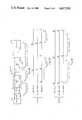
- the detector 16is, for example, a parallel amplifier array of 10 4 elements 30 arranged in rows and columns of 100 elements each.
- Each elementincludes a solid state switch 32, and a capacitor 34.
- Switches 32may be, for example, field effect transistors (FETs) formed by diffusing for each switch two N-type regions, called the drain 36 and the source 38, side by side into the surface of a P-type silicon slice. A layer of silicon oxide is grown over the surface of the silicon slice and metal strips are formed on the oxides to form the gates 40.
- the capacitors 34are formed, for example, of a wafer of ferroelectric material having longitudinal lead patterns 42 and pads 44 formed on opposing major surfaces by evaporation/etching techniques. The pads and the crossover portions of the lead patterns form the plates of the capacitors 34 with the ferroelectric material forming the dielectric.
- the gates 40 of the switches 32 of each roware connected by leads 46 to a Y addressing circuit 47 and the sources and drains are connected by leads 48 and 50, respectively, to the first plates 44 of capacitors 34 and to the reset lines 54 of reset switches 56 and of amplifier chain circuits 58.
- the inherent capacitors of the sense lines 54are shown as capacitors 57.
- the second plates 42 of capacitors 34are connected by leads 52 to v-bias.
- the reset switches 56are, for example, FET switches having their gates 60 connected by lead 61 to a reset voltage source (not shown).
- the reset circuitis to charge the capacitors 34 to a reference voltage when shielded from light (photons) by the chopper.
- the amplifier chain circuits 58are connected to the drains of the FET switches 62.
- Switches 62have their gates 63 connected to an X-addressing circuit 64 and their sources connected to output lead 66.
- each of the amplifier chain circuits 58includes a common source metal oxide semiconductor (MOS) amplifier (low noise front stages) 68 (FIG. 3a) connected to a sense lead 54 (FIG. 2).
- a double correlation sample filter (DCS) 70is connected to the output of the low noise front stages 68.
- the DCS filter 70includes a resistor 72 connected to the junction of capacitors 74 and 76.
- Capacitor 74is grounded and capacitor 76 is connected to the junction of a DCS clamp 78 and amplifier 80.
- Clamp 78is a FET switch which is turned on to store preamplifier noise on capacitor 74 and off to discharge the capacitor 74 into the load.
- Amplifier 80is to restore the filtered signal.
- Amplifier 80has its output connected to the junction of positive and negative sample and hold (S&H) circuits 82 and 84.
- S&Hpositive and negative sample and hold
- the positive S&H circuit 82includes a FET switch 86 connected to the junction of a capacitor 88 and amplifier 90.
- the capacitor 88is grounded and the amplifier 90 has its output connected to capacitor 92.
- the negative S&H circuit 84includes a FET switch 94 having its source connected to the junction of capacitor 96 and inverter amplifier 98.
- Inverter amplifier 98has a gain of -C s /(C d +C s ) times that of amplifier 90 and has its output connected to capacitor 100.
- a secondary clamp 102which is a FET switch, has its source connected to the junction of capacitors 92 and 100 and amplifier 104. The FET switch of the secondary clamp can be turned on to establish a volage reference across capacitors 92 and 100.
- the multiplexed output of amplifier 104is connected to the junction of off chip electronics 107 for removal of the reset noise on output lead 66.
- the off chip electronics 107includes a storage means 106 connected by lead 105 to receive the multiplexed outputs of the amplifiers 104 and to the negative terminal of a summing (differencing) amplifier 108.
- the positive terminal of amplifier 108is connected to receive the multiplexed outputs of amplifier 104s of multiplexer 64.
- the output of amplifier 108is connected to monolithic delta frame 22 (FIG. 1) for removal of the fixed offset noise and conversion of the pixel rate.
- the storage means 106 (FIG. 3a) and differencing amplifier 108 of off chip electronics 107preferable is a monolithic delta frame 20 which is capable of performing the required reset noise storage and subtraction.
- the total subtraction amplifier chainis to substantially cancel reset noise that exists in the detector array.
- Reset noise in a detector arrayexists owing to the uncertainty in voltage appearing across a capacitor as that capacitor is being charged by a resistive source.
- the root mean square (RMS) voltage uncertainties due to reset action on detector and sense node capacitances in a detectorare given by (KT/C d ) 1/2 , and (KT/C s ) 1/2 , respectively, where K is Boltzman's constant, T is the time, C d is the capacitance of the detector and C s is the capacitance of the sense line 54.
- While the RMSrepresents average noise the present invention utilizes the individual events of this RMS term. The individual events are determined and subtracted by the above circuit.
- the detector capacitanceis completely reset in two parts.
- the reset switch 56(FIG. 2) resets C d and C s together and then in the second part (2) the C d is separated from C s by the opening of the address switch 32.
- (KT/C d ) 1/2 volts of RMS noiseis left on the detector, this method of reset is required to sense the specific values of these noise events by indirect means.
- the noise storage means 106must be capable of storing a noise sample from every detector in the array (an entire frame of noise line data) for comparison with the next frames.
- storage and differencing meanssuch as, for example, a monolithic delta (difference) frame device is used as the off chip electronics 107.
- the monolithic delta frames 20 and 22are identical in construction; thus, only one need be described.
- the monolithic delta frame(FIG. 4) includes a high speed line address circuit 110.
- a demultiplexer 112is connected to the high speed address circuit and to the video output of amplifier 104 (FIG. 3a).
- a line shift means 114(FIG. 4) is connected to the demultiplexer 112.
- a plurality (100) of buffer amplifiers 116are connected to the line shift register 114. Rows of elements 118 are connected to the plurality of buffer amplifiers.
- Each element 118includes a capacitor 120 and a switch 122.
- the buffer amplifier 116is connected to one plate of the capacitor 120.
- the switch 122is a FET switch having its drain connected to a second plate of the capacitor, its gate connected by lead 124 to a low speed column (Y) address register 126 and its source connected by lead 128 to a reset circuit element 130. Again, there is one element 130 for each row (100 rows).
- Each line reset elementincludes a FET switch 132 having its gate connected to line reset lead 134, its source connected to the junction of lead 128 and amplifier 136 and S&H circuits 138. S&H circuits 138 are connected to a multiplexer 139.
- a high speed line address register 140is connected to the multiplexer 139 for controlling its video output signals through video out terminal 142.
- Monolithic delta frame 22has its video in terminal connected to the video out terminal 142 of monolithic delta frame 20.
- the monolithic delta frame 20performs the noise storage and subtraction functions; while, monolithic delta frame 22 accomplishes the offset suppression and 2x/1x conversion.
- monolithic delta frame 20the use of the high impedance buffer 136 on each line 128 lowers the line parasitics and the additional capacitance created by the line buffers is substantially reduced by the source follower input stage. Because of this parasitic reduction, the required capacitance of the storage capacitors 120 is low so that they may be built into the metal oxide semiconductor (MOS) IC using standard processing; hence, the name Monolithic or Integrated Delta Frame.
- MOSmetal oxide semiconductor
- the circuit element 130is a high-gain inverting output amplifier chain with dc feedback to suppress amplifier fixed-pattern noise offsets in a dc coupled multiplexer 138.
- the 2x to 1x speed conversion ratecan be made at either monolithic delta frame 20 or 22 by including S&H circuits 138 having common gate connections.
- the detector 16 outputis clocked into and out of the monolithic delta frame 20 and into the monolithic delta frame 22 at a 2x rate (FIG. 5b).
- the output of monolithic delta frame 22(FIG. 5c) is clocked out at 1x rate to the display 26.
- the term "column shift”refers to the shift command given to the low-speed column address shift register 126 (FIG. 4).
- the arguments X and Y FIGS. 5b & 5c)refer to the frame and column numbers, respectively, and the S to the signal.
- the timing diagram for monolithic delta frame 20indicates that the storage command for monolithic delta frame 20 takes place only after a noise line has been shifted into the matrix by the line shift pulse. Thus fulfilling the noise storage requirement when an S+N line is shifted into the capacitor matrix thereof.
- this monolithic frame detectoris an improvement over the "Delta Frame Circuit" of U.S. Pat. No. 4,178,612, issued Dec. 11, 1979.
- the transversal filter 24 (FIG. 6) of the second embodimentis connected to the second monolithic delta frame circuit 22 (FIG. 1) for peak signal detection to improve display resolution. It includes, for example, a 6-stage, 1 bit free-running digital shift register 150 (FIG. 6) connected to a corresponding number of sets (6) of S&H circuits 152.
- the sets of S&H circuitsare connected to the output of the second monolithic delta frame 22 (FIG. 1) for receiving the video inputs and to a corresponding number of sets of line driver amplifiers 154 (FIG. 6) to a corresponding number of sets of output switches 156.
- Each set of S&H circuits 152contain five S&H circuits connected to five consecutive bits of the shift register 150.
- Each set of line drivers 154includes five amplifiers connected to the five S&H circuits of each corresponding set thereof. While, each set of output switches 156 has five transistor switches connected to the five amplifiers of each corresponding set thereof. The sixth bit of the shift register 150 is selectively connected to each set of output switches 156 for sequentially operating each set of output switches.
- Five voltage weighting circuits 158are connected to the five output switches of each set of output switches, and the outputs of the weighting circuits are connected to a summer 160. The output of the summer 160 is connected to the display 26 (FIG. 1).
- the transversal filter 24has its S&H circuits connected to the single line video output of monolithic delta frame 22 and performs a peaking function thereon.
- the six stage, 1 bit shift register 150addresses sequentially the six sets of S&H circuits 152 to store each pixel of information in five places simultaneously (see Table 2).
- the sixth bitis used to read out a set of S&H circuits when the correct sequence of pixels is stored in that set.
- the five pixels of the set read outare voltage weighted by the weighting circuits 158 and applied to the summer 160. Pixel tracing is shown in Table 3.
- pixel 1is stored simultaneously in S&H circuits 152, stages 1,3,4,5 and 6 at pin locations 1,5,4,3, and 2, respectively; the switch out bit is connected to stage 2, pin 6.
- the remaining pixels 2-5 for one frame together with the switch out bitare sequentially stored at succeeding pin locations of the stages for the first cycle.
- the number of stagesdetermines the length of the filter.
- switch out of stage 1occurs, pixels 1-5 are weighted in weighting circuits 158 and summed by summer 160 for providing peak voltage for pixel 1, while, pixel 6 is stored in positions 5-1 of stages 2-6, respectively.
- stages 2-6are read out for weighting pixels 2-6 to complete the cycle.
- the cycleis repeated to input pixels 7-12 to determine their peak value and thereafter the cycle repeated until completion.
Landscapes
- Engineering & Computer Science (AREA)
- Multimedia (AREA)
- Signal Processing (AREA)
- Health & Medical Sciences (AREA)
- Toxicology (AREA)
- Transforming Light Signals Into Electric Signals (AREA)
Abstract
Description
[(C.sub.d /C.sub.d +C.sub.s).sup.2 KT/C.sub.d +(C.sub.s /C.sub.d +C.sub.s).sup.2 KT/C.sub.s ].sup.1/2 =(KT/C.sub.d +C.sub.s).sup.1/2 =RMS
TABLE 1 __________________________________________________________________________AFTER NOISE VOLTAGE EXCURSION EVENT ON DETECTOR ON SENSE NODE __________________________________________________________________________1N1 N1 2 N1 + N2 N1 - (C.sub.d /C.sub.s)N2 3 N1 + N2 + SIG N3 4 C.sub.d /(C.sub.d + C.sub.s)(N1 + N2 + SIG) + C.sub.s N3/C.sub.d + C.sub.s C.sub.d /(CD + C.sub.s)(N1 + N2 + SIG) + C.sub.s N3/C.sub.d + C.sub.s __________________________________________________________________________
S1=N1
S2=N1-C.sub.d /C.sub.s N2
S3=N3
S4=C.sub.d /(C.sub.d +C.sub.s)(N1+N2+SIG)+C.sub.s /(C.sub.d +C.sub.s)N3
S4-C.sub.s /(C.sub.d +C.sub.s)(S3-S2)-S1=C.sub.d /(C.sub.d +C.sub.s)Sig
TABLE 2 __________________________________________________________________________S REG.STAGE # 1STAGE # 2 STAGE #3 STAGE #4 STAGE #5 STAGE #6 OUTPUT S & H NODE S & H NODE S & H NODE S & H NODE S & H NODE S & H NODE __________________________________________________________________________1 1 SW OUT 5 4 3 2 2 2 1 SW OUT 5 4 3 3 3 2 1 SW OUT 5 4 4 4 3 2 1 SW OUT 5 5 5 4 3 2 1 SW OUT 6 SW OUT 5 4 3 2 1 __________________________________________________________________________
TABLE 3 __________________________________________________________________________STAGE # 1STAGE # 2 STAGE #3 STAGE #4 STAGE #5 STAGE #6 PIXEL S & H NODE S & H NODE S & H NODE S & H NODE S & H NODE S & H NODE __________________________________________________________________________1 1 SW OUT 5 4 3 2 2 2 1 SW OUT 5 4 3 3 3 2 1 SW OUT 5 4 4 4 3 2 1 SW OUT 5 5 5 4 3 2 1 SW OUT 6 SW OUT 5 4 3 2 1 7 1 SW OUT 5 4 3 2 8 2 1 SW OUT 5 4 3 9 3 2 1 SW OUT 5 4 10 4 3 2 1 SW OUT 5 11 5 4 3 2 1 SW OUT 12 SW OUT 5 4 3 2 1 13 1 SW OUT 5 4 3 2 14 2 1 SW OUT 5 4 3 15 3 2 1 SW OUT 5 4 16 4 3 2 1 SW OUT 5 17 5 4 3 2 1 SW OUT __________________________________________________________________________
Claims (11)
Priority Applications (3)
| Application Number | Priority Date | Filing Date | Title |
|---|---|---|---|
| US06/638,832US4617593A (en) | 1984-08-07 | 1984-08-07 | Visible and near infrared imaging system |
| EP85108496AEP0170908B1 (en) | 1984-08-07 | 1985-07-09 | Visible and near infrared imaging system |
| DE8585108496TDE3587163T2 (en) | 1984-08-07 | 1985-07-09 | IMAGE RECORDING SYSTEM FOR VISIBLE AND CLOSE-INFRARED LIGHT. |
Applications Claiming Priority (1)
| Application Number | Priority Date | Filing Date | Title |
|---|---|---|---|
| US06/638,832US4617593A (en) | 1984-08-07 | 1984-08-07 | Visible and near infrared imaging system |
Publications (1)
| Publication Number | Publication Date |
|---|---|
| US4617593Atrue US4617593A (en) | 1986-10-14 |
Family
ID=24561636
Family Applications (1)
| Application Number | Title | Priority Date | Filing Date |
|---|---|---|---|
| US06/638,832Expired - LifetimeUS4617593A (en) | 1984-08-07 | 1984-08-07 | Visible and near infrared imaging system |
Country Status (3)
| Country | Link |
|---|---|
| US (1) | US4617593A (en) |
| EP (1) | EP0170908B1 (en) |
| DE (1) | DE3587163T2 (en) |
Cited By (20)
| Publication number | Priority date | Publication date | Assignee | Title |
|---|---|---|---|---|
| US4987321A (en)* | 1989-09-25 | 1991-01-22 | Eastman Kodak Company | Processing circuit for image sensor |
| US5010408A (en)* | 1989-09-25 | 1991-04-23 | Eastman Kodak Company | Doubly correlated sample and hold circuit |
| US5349380A (en)* | 1991-10-15 | 1994-09-20 | Hughes Aircraft Company | Resettable clamp-sample-and-hold signal processing circuit for imaging sensors |
| WO1995020750A1 (en)* | 1994-01-26 | 1995-08-03 | Försvarets Forskningsanstalt | Sensor device |
| US5548329A (en)* | 1992-09-29 | 1996-08-20 | Hughes Aircraft Company | Perceptual delta frame processing |
| EP0699880A3 (en)* | 1992-08-13 | 1996-09-11 | Bodenseewerk Geraetetech | Refrigeration system for cooling a sensor situated in the jacket void of a Dewar vessel |
| US5729285A (en)* | 1993-07-27 | 1998-03-17 | Texas Instruments Incorporated | Focal plane array integrated circuit with individual pixel signal processing |
| US20140332665A1 (en)* | 2010-04-21 | 2014-11-13 | Sionyx, Inc. | Photosensitive imaging devices and associated methods |
| US9374563B2 (en) | 2012-11-01 | 2016-06-21 | Raytheon Company | Multispectral imaging camera |
| US9496308B2 (en) | 2011-06-09 | 2016-11-15 | Sionyx, Llc | Process module for increasing the response of backside illuminated photosensitive imagers and associated methods |
| US9673243B2 (en) | 2009-09-17 | 2017-06-06 | Sionyx, Llc | Photosensitive imaging devices and associated methods |
| US9673250B2 (en) | 2013-06-29 | 2017-06-06 | Sionyx, Llc | Shallow trench textured regions and associated methods |
| US9761739B2 (en) | 2010-06-18 | 2017-09-12 | Sionyx, Llc | High speed photosensitive devices and associated methods |
| US9762830B2 (en) | 2013-02-15 | 2017-09-12 | Sionyx, Llc | High dynamic range CMOS image sensor having anti-blooming properties and associated methods |
| US9905599B2 (en) | 2012-03-22 | 2018-02-27 | Sionyx, Llc | Pixel isolation elements, devices and associated methods |
| US9911781B2 (en) | 2009-09-17 | 2018-03-06 | Sionyx, Llc | Photosensitive imaging devices and associated methods |
| US9939251B2 (en) | 2013-03-15 | 2018-04-10 | Sionyx, Llc | Three dimensional imaging utilizing stacked imager devices and associated methods |
| US10244188B2 (en) | 2011-07-13 | 2019-03-26 | Sionyx, Llc | Biometric imaging devices and associated methods |
| US10361083B2 (en) | 2004-09-24 | 2019-07-23 | President And Fellows Of Harvard College | Femtosecond laser-induced formation of submicrometer spikes on a semiconductor substrate |
| US10374109B2 (en) | 2001-05-25 | 2019-08-06 | President And Fellows Of Harvard College | Silicon-based visible and near-infrared optoelectric devices |
Families Citing this family (3)
| Publication number | Priority date | Publication date | Assignee | Title |
|---|---|---|---|---|
| CH669699A5 (en)* | 1986-02-20 | 1989-03-31 | Gx Holding Ag | |
| JP3287056B2 (en)* | 1993-03-24 | 2002-05-27 | ソニー株式会社 | Solid-state imaging device |
| CN111651630B (en)* | 2020-05-31 | 2023-12-26 | 广西电网有限责任公司南宁供电局 | Method for improving storage efficiency of acquisition dynamic infrared thermal map by adopting key data frame |
Citations (2)
| Publication number | Priority date | Publication date | Assignee | Title |
|---|---|---|---|---|
| US4178612A (en)* | 1978-07-21 | 1979-12-11 | Texas Instruments Incorporated | Delta frame circuit |
| US4379232A (en)* | 1977-12-19 | 1983-04-05 | Texas Instruments Incorporated | Ferroelectric imaging system |
Family Cites Families (2)
| Publication number | Priority date | Publication date | Assignee | Title |
|---|---|---|---|---|
| JPS5822900B2 (en)* | 1978-09-25 | 1983-05-12 | 株式会社日立製作所 | solid-state imaging device |
| DE2842980A1 (en)* | 1978-10-02 | 1980-04-17 | Bosch Gmbh Robert | Interference components elimination in thermal camera video signal - involves periodically interrupting thermal flow and signal is delayed and further processed |
- 1984
- 1984-08-07USUS06/638,832patent/US4617593A/ennot_activeExpired - Lifetime
- 1985
- 1985-07-09DEDE8585108496Tpatent/DE3587163T2/ennot_activeExpired - Fee Related
- 1985-07-09EPEP85108496Apatent/EP0170908B1/ennot_activeExpired - Lifetime
Patent Citations (2)
| Publication number | Priority date | Publication date | Assignee | Title |
|---|---|---|---|---|
| US4379232A (en)* | 1977-12-19 | 1983-04-05 | Texas Instruments Incorporated | Ferroelectric imaging system |
| US4178612A (en)* | 1978-07-21 | 1979-12-11 | Texas Instruments Incorporated | Delta frame circuit |
Cited By (34)
| Publication number | Priority date | Publication date | Assignee | Title |
|---|---|---|---|---|
| US5010408A (en)* | 1989-09-25 | 1991-04-23 | Eastman Kodak Company | Doubly correlated sample and hold circuit |
| US4987321A (en)* | 1989-09-25 | 1991-01-22 | Eastman Kodak Company | Processing circuit for image sensor |
| US5349380A (en)* | 1991-10-15 | 1994-09-20 | Hughes Aircraft Company | Resettable clamp-sample-and-hold signal processing circuit for imaging sensors |
| EP0699880A3 (en)* | 1992-08-13 | 1996-09-11 | Bodenseewerk Geraetetech | Refrigeration system for cooling a sensor situated in the jacket void of a Dewar vessel |
| US5548329A (en)* | 1992-09-29 | 1996-08-20 | Hughes Aircraft Company | Perceptual delta frame processing |
| US5729285A (en)* | 1993-07-27 | 1998-03-17 | Texas Instruments Incorporated | Focal plane array integrated circuit with individual pixel signal processing |
| WO1995020750A1 (en)* | 1994-01-26 | 1995-08-03 | Försvarets Forskningsanstalt | Sensor device |
| US10374109B2 (en) | 2001-05-25 | 2019-08-06 | President And Fellows Of Harvard College | Silicon-based visible and near-infrared optoelectric devices |
| US10741399B2 (en) | 2004-09-24 | 2020-08-11 | President And Fellows Of Harvard College | Femtosecond laser-induced formation of submicrometer spikes on a semiconductor substrate |
| US10361083B2 (en) | 2004-09-24 | 2019-07-23 | President And Fellows Of Harvard College | Femtosecond laser-induced formation of submicrometer spikes on a semiconductor substrate |
| US10361232B2 (en) | 2009-09-17 | 2019-07-23 | Sionyx, Llc | Photosensitive imaging devices and associated methods |
| US9673243B2 (en) | 2009-09-17 | 2017-06-06 | Sionyx, Llc | Photosensitive imaging devices and associated methods |
| US9911781B2 (en) | 2009-09-17 | 2018-03-06 | Sionyx, Llc | Photosensitive imaging devices and associated methods |
| US20190206923A1 (en)* | 2010-04-21 | 2019-07-04 | Sionyx, Llc | Photosensitive imaging devices and associated methods |
| US11264371B2 (en)* | 2010-04-21 | 2022-03-01 | Sionyx, Llc | Photosensitive imaging devices and associated methods |
| US20170358621A1 (en)* | 2010-04-21 | 2017-12-14 | Sionyx, Llc | Photosensitive imaging devices and associated methods |
| US20140332665A1 (en)* | 2010-04-21 | 2014-11-13 | Sionyx, Inc. | Photosensitive imaging devices and associated methods |
| US9741761B2 (en)* | 2010-04-21 | 2017-08-22 | Sionyx, Llc | Photosensitive imaging devices and associated methods |
| US10748956B2 (en)* | 2010-04-21 | 2020-08-18 | Sionyx, Llc | Photosensitive imaging devices and associated methods |
| US10229951B2 (en)* | 2010-04-21 | 2019-03-12 | Sionyx, Llc | Photosensitive imaging devices and associated methods |
| US10505054B2 (en) | 2010-06-18 | 2019-12-10 | Sionyx, Llc | High speed photosensitive devices and associated methods |
| US9761739B2 (en) | 2010-06-18 | 2017-09-12 | Sionyx, Llc | High speed photosensitive devices and associated methods |
| US9666636B2 (en) | 2011-06-09 | 2017-05-30 | Sionyx, Llc | Process module for increasing the response of backside illuminated photosensitive imagers and associated methods |
| US10269861B2 (en) | 2011-06-09 | 2019-04-23 | Sionyx, Llc | Process module for increasing the response of backside illuminated photosensitive imagers and associated methods |
| US9496308B2 (en) | 2011-06-09 | 2016-11-15 | Sionyx, Llc | Process module for increasing the response of backside illuminated photosensitive imagers and associated methods |
| US10244188B2 (en) | 2011-07-13 | 2019-03-26 | Sionyx, Llc | Biometric imaging devices and associated methods |
| US10224359B2 (en) | 2012-03-22 | 2019-03-05 | Sionyx, Llc | Pixel isolation elements, devices and associated methods |
| US9905599B2 (en) | 2012-03-22 | 2018-02-27 | Sionyx, Llc | Pixel isolation elements, devices and associated methods |
| US9374563B2 (en) | 2012-11-01 | 2016-06-21 | Raytheon Company | Multispectral imaging camera |
| US9762830B2 (en) | 2013-02-15 | 2017-09-12 | Sionyx, Llc | High dynamic range CMOS image sensor having anti-blooming properties and associated methods |
| US9939251B2 (en) | 2013-03-15 | 2018-04-10 | Sionyx, Llc | Three dimensional imaging utilizing stacked imager devices and associated methods |
| US10347682B2 (en) | 2013-06-29 | 2019-07-09 | Sionyx, Llc | Shallow trench textured regions and associated methods |
| US11069737B2 (en) | 2013-06-29 | 2021-07-20 | Sionyx, Llc | Shallow trench textured regions and associated methods |
| US9673250B2 (en) | 2013-06-29 | 2017-06-06 | Sionyx, Llc | Shallow trench textured regions and associated methods |
Also Published As
| Publication number | Publication date |
|---|---|
| EP0170908B1 (en) | 1993-03-10 |
| EP0170908A3 (en) | 1988-01-07 |
| DE3587163D1 (en) | 1993-04-15 |
| EP0170908A2 (en) | 1986-02-12 |
| DE3587163T2 (en) | 1993-08-19 |
Similar Documents
| Publication | Publication Date | Title |
|---|---|---|
| US4617593A (en) | Visible and near infrared imaging system | |
| US6753912B1 (en) | Self compensating correlated double sampling circuit | |
| EP1515540B1 (en) | Semiconductor device, and control method and device for driving unit component of semiconductor device | |
| US5083016A (en) | 3-transistor source follower-per-detector unit cell for 2-dimensional focal plane arrays | |
| US6046444A (en) | High sensitivity active pixel with electronic shutter | |
| EP0493455B1 (en) | I.c. sensor | |
| JP4362156B2 (en) | Sequential correlation double sampling method for CMOS area array sensor | |
| NO965104D0 (en) | Device, system and method for reflecting an image | |
| US6441357B2 (en) | Using cascaded gain stages for high-gain and high-speed readout of pixel sensor data | |
| US4233632A (en) | Solid state image pickup device with suppressed so-called blooming phenomenon | |
| US20110013045A1 (en) | Cmos image sensor with processor controlled integration time | |
| US6950131B1 (en) | Simultaneous access and reset system for an active pixel sensor | |
| US4667239A (en) | Signal peaking device for single-line video input | |
| US4622587A (en) | Monolithic delta frame circuit | |
| US4806779A (en) | Solid-state image pickup apparatus using static induction transistors for performing non-destructive readout | |
| KR19990072919A (en) | Solid state image pickup device, driving method therefor and camera | |
| EP0766257A1 (en) | Analog memory for storing a QCIF image or the like as electric charge | |
| US6798452B1 (en) | Amplifying solid-state imaging device, method for driving the same and physical quantity distribution sensing semiconductor device | |
| US5847599A (en) | Stable fast settling sense amplifier | |
| JPH10190987A (en) | Output circuit of a solid-state image-pickup device and drive method therefor | |
| GB2250089A (en) | Spectrometer | |
| JP3038985B2 (en) | Image sensor | |
| JPH04880A (en) | Solid-state image pickup device | |
| Ricquier et al. | CIVIS sensor: a flexible smart imager with programmable resolution | |
| JPH02107076A (en) | Solid-state image pickup device |
Legal Events
| Date | Code | Title | Description |
|---|---|---|---|
| AS | Assignment | Owner name:TEXAS INSTRUMENTS INCORPORATED, 13500 NORTH CENTRA Free format text:ASSIGNMENT OF ASSIGNORS INTEREST.;ASSIGNOR:DUDLEY, DANA;REEL/FRAME:004366/0106 Effective date:19840801 | |
| STCF | Information on status: patent grant | Free format text:PATENTED CASE | |
| FEPP | Fee payment procedure | Free format text:PAYOR NUMBER ASSIGNED (ORIGINAL EVENT CODE: ASPN); ENTITY STATUS OF PATENT OWNER: LARGE ENTITY | |
| FPAY | Fee payment | Year of fee payment:4 | |
| FPAY | Fee payment | Year of fee payment:8 | |
| FEPP | Fee payment procedure | Free format text:PAYOR NUMBER ASSIGNED (ORIGINAL EVENT CODE: ASPN); ENTITY STATUS OF PATENT OWNER: LARGE ENTITY Free format text:PAYER NUMBER DE-ASSIGNED (ORIGINAL EVENT CODE: RMPN); ENTITY STATUS OF PATENT OWNER: LARGE ENTITY | |
| AS | Assignment | Owner name:RAYTHEON TI SYSTEMS, INC., TEXAS Free format text:ASSIGNMENT OF ASSIGNORS INTEREST;ASSIGNORS:TEXAS INSTRUMENTS INCORPORATED;TEXAS INSTRUMENTS DEUTSCHLAND GMBH;REEL/FRAME:008628/0414 Effective date:19970711 | |
| FPAY | Fee payment | Year of fee payment:12 | |
| AS | Assignment | Owner name:RAYTHEON COMPANY, A CORPORATION OF DELAWARE, MASSA Free format text:CHANGE OF NAME;ASSIGNOR:RAYTHEON TI SYSTEMS, INC.;REEL/FRAME:009875/0499 Effective date:19981229 |