US4613953A - Paging register for memory devices - Google Patents
Paging register for memory devicesDownload PDFInfo
- Publication number
- US4613953A US4613953AUS06/487,554US48755483AUS4613953AUS 4613953 AUS4613953 AUS 4613953AUS 48755483 AUS48755483 AUS 48755483AUS 4613953 AUS4613953 AUS 4613953A
- Authority
- US
- United States
- Prior art keywords
- address
- lines
- page
- signals
- size
- Prior art date
- Legal status (The legal status is an assumption and is not a legal conclusion. Google has not performed a legal analysis and makes no representation as to the accuracy of the status listed.)
- Expired - Lifetime
Links
Images


Classifications
- G—PHYSICS
- G06—COMPUTING OR CALCULATING; COUNTING
- G06F—ELECTRIC DIGITAL DATA PROCESSING
- G06F12/00—Accessing, addressing or allocating within memory systems or architectures
- G06F12/02—Addressing or allocation; Relocation
- G06F12/0223—User address space allocation, e.g. contiguous or non contiguous base addressing
- G—PHYSICS
- G06—COMPUTING OR CALCULATING; COUNTING
- G06F—ELECTRIC DIGITAL DATA PROCESSING
- G06F12/00—Accessing, addressing or allocating within memory systems or architectures
- G06F12/02—Addressing or allocation; Relocation
- G06F12/06—Addressing a physical block of locations, e.g. base addressing, module addressing, memory dedication
- G06F12/0615—Address space extension
- G06F12/0623—Address space extension for memory modules
Definitions
- the present inventionrelates to a microcomputer addressing and control system for operatively addressing a mass memory so that the memory can be partitioned into selectable pages of individually specified size.
- the inventionis directed toward an application in which the addressable content of the whole mass memory exceeds the addressing size available to the microcomputer, whereas the information within the mass memory actually resides in blocks whose individual address size is compatible with the address size available to the microcomputer.
- the inventioncontemplates a high speed, semiconductor, chip type mass memory, such as a large read only memory (ROM) chip, having a data content significantly exceeding the available address size of the microcomputer system connected thereto.
- the corresponding circuit implementation of the mass memory addressing and control systemutilizes a memory control register to receive and hold page size and page select information off a multiplexed data bus.
- a decode circuit connected to the address businitiates a latch of the page size and select information into the memory control register when a specified bit code appears on the address bus coincident with a defined chip select line signal.
- the page address information in the page selection register of the memory control register, as well as various address bus lines,are connected to the mass memory via a memory control multiplexer.
- the size address informationis coupled to the memory control multiplexer to prescribe and limit the page address bit code coupled to the mass memory within the page size limits established.
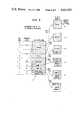
- FIG. 1is a block diagram schematically depicting one embodiment of the mass memory addressing and control system.
- FIG. 2is a schematic diagram of six different address maps suitable to interface a 16K byte ROM or RAM mass memory with a microcomputer having 4K available address.
- FIGS. 3A and 3Btogether form a circuit schematic embodying one variation of the features in the present invention.
- a typical microcomputer systemmay have sufficient address remaining for a single operating program, such as either BASIC or PASCAL, but not for both these and other programs of potential interest to the microcomputer user. It is obviously possible to resort to mechanically implemented mass storage configurations to retain the diverse programs sought, and to transfer the selected program into internal RAM during each microcomputer program operation.
- the utilization of peripheral systemsinherently introduces the deficiencies noted earlier.
- the addressing and control system in FIG. 1also includes a memory control register, 8, comprised of page size register 9 and page select register 11.
- Registers 9 and 11are connected to data bus 4 using respective buses 12 and 13.
- the data appearing on bus lines 12 and 13is latched into respective registers 9 and 11 by a latch command signal, on register latch line 14, generated in decode block 16. It should be recognized that the bit code latched into the size and page registers remains operative until the succeeding register latch signal. Consequently, the data code on size bus 17 and page bus 18 from respective registers 9 and 11 can remain for an unlimited sequence of addressing operations performed over address bus 21.
- the read/write line, 7, entering decode 16 and memory array 1depicts the arrangement used with a RAM type array. It should be appreciated that the connection of the read/write lines to decode 16, and operationally to memory control register 8, is added for a circuit configuration in which the states of the registers in memory control register 8 are to be interrogated over data bus 4. This variant will be developed in greater detail at a later point.
- memory control multiplexer 22The remaining element to be considered in the block diagram of FIG. 1 is memory control multiplexer 22. As embodied, memory control multiplexer 22 multiplexes the bit content of upper address bus 23 and page bus 18 on the basis of the bit code on size bus 17. The output from memory control multiplexer 22 appears on upper address bus 2, which when combined with lower address bus 3 generates the composite address for selecting data from within memory array 1.
- upper address bus 23may be wholly or partially deleted, such as would occur in an application where the number of address lines required to select data from memory array 1 was greater than the size of address bus 21.
- the data bus 4would be utilized to provide the supplemental bits necessary to complement the address on line 3 so that the bit length would be compatible with the size of memory array 1. Consequently, it should be understood that the sizes of the various buses in FIG. 1 are merely illustrative of a convenient and readily comprehensible configuration.
- FIGS. 2, 3A and 3BTo illustrate the various features and implications of the functional configuration depicted in FIG. 1, attention is now directed to FIGS. 2, 3A and 3B for a detailed development of the embodiment.
- the illustration in FIG. 2provides a conceptual presentation of the memory mapping performed by the present address and control system.
- FIGS. 3A and 3Billustrate a corresponding circuit implementation.
- the reference numerals attributed to functional elements in FIG. 1will be employed to designate corresponding operative circuit elements in FIGS. 3A and 3B.
- the memory mapping depicted in FIG. 2is based on an embodiment in which the microcomputer system has 4K of unallocated address, yet wishes to address groups of information from a mass memory of 16K bytes. For instance, this would correspond to a microcomputer having an overall address capacity of 8K in which 4K is fully allocated to RAM address and internal control functions. Nevertheless, the microcomputer user wishes, by way of this example, to have the flexibility of selectively operating the microcomputer using programs such as PASCAL, BASIC or VISICALC (a registered trademark of Visicorp), various games, and an addressable data base, while remaining within the confines of the microcomputer hardware.
- programssuch as PASCAL, BASIC or VISICALC (a registered trademark of Visicorp)
- ROM 1is partitioned into eight 2K segments, numbered 0-7, of which the first 4K correspond to the PASCAL program, the second 4K correspond to the BASIC program, the succeeding 3K correspond to the VISICALC program, the next 1K correspond to GAME I, the next 2K correspond to GAME II, the following 1K correspond to a DATA BASE, and the final 1K are unprogrammed.
- the programscan be larger or smaller than the segments. Consequently, if memory mapping is to be accomplished by page, the size of a page can be equal to or greater than the individual 2K segments of ROM 1.
- map number 1representing the mapping of the 4K size PASCAL program as a single page.
- the whole ROMis partitioned into four pages of 4K size each, so that segments 0 and 1 are mapped simultaneously as a single page.
- the page sizeremains at 4K for the VISICALC program of map number 3, where the ROM segments 4 and 5 are address mapped.
- GAME Iis mapped together with the VISICALC program, allowing access thereto through map number 3 given that the correct addresses are utilized during microcomputer operation.
- Maps 4, 5 and 6utilize 2K size pages, requiring that ROM 1 be partitioned into eight segments.
- Address map number 4conveys GAME I and part of the VISICALC program, so that GAME I is distinguished by means of the address itself.
- map number 5the whole of GAME II is mapped, with remaining microprocessor address being uncommitted.
- map number 6the 1K DATA BASE is mapped in the same manner.
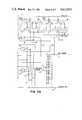
- the 16K byte memory array, 1,is shown in FIG. 3A to have a number of electrical connections: 14 address input lines, A0-A10 and A11'-A13'; eight data output lines, D0-D7; memory enable line 6; and read/write line 7 for the RAM configuration. Note the correspondence of reference numerals as to the address and data buses, with respect to FIG. 1.
- Page register 11 in FIG. 3Bis shown to be comprised of three D-type flip-flops, 24, 26 and 27.
- the D-inputs to the flip-flopsare connected to data bus 4 lines D0-D2.
- the Q outputs from the flip-flopsappear on lines 28, 29 and 31.
- Size register 9, immediately adjacent to page register 11,is shown to consist of two flip-flops, 32 and 33, and is connected to data bus 4 via lines D3 and D4, respectively.
- the size register Q output signalsappear on lines 34 and 36.
- all D-type flip-flopsare rising edge triggered.
- all register flip-flopsare latched by a common signal on register latch line 14, a signal generated in decode OR gate 37.
- the sequence of signals preceding the latching of data from bus lines D0-D4 into registers 9 and 11begins with an address bus code, on lines A0-A13, of low level signals coinciding with a low level signal on chip select line 19.
- This combinationgenerates a low level signal on register latch line 14, which upon further combination through inverter block 38 and AND gate 39 also generates a low level signal on memory enable line 6 to disable memory array 1.
- Memory array 1is disabled to make data bus 4 available for the size and page register information provided on lines D0-D4 thereof.
- the bit code from size register 9 on lines 34 and 36defines, and effectively multiplexes, the code on bus lines A11, A12, and A13 with page register lines 28, 29 and 31, depending on the page size prescribed, to generate a mapped address for memory address input lines A11', A12' and A13'.
- the logic blocks by which this is implementedare depicted in FIGS. 3A and 3B, where gates 41, 42, 43, 44 and 46 combine to generate the memory address signal on line A13'; gates 47, 48, 49 and 51 combine to generate the memory address signal on line A12'; and gates 52, 53, 54, 56 and 57 combine to generate the memory address signal on line A11'.
- the various bit codes which define the memory array addresses according to the circuit in FIGS. 3A and 3Bare prescribed according to Tables A, B, and C, which follow.
- the formation of the bit code data (D0-D4) which selects the program content and size of the mappingis performed in conventional manner, in the sense of generating an extended address.
- Table Cshows that the signal on line A11 of address bus 21 is coupled to input line A11' of memory array 1 when the page size is established at 4K.
- the circuit in FIGS. 3A and 3Balso couples lines A12 to input line A12' for an 8K size page, and further couples line A13 to line A13' for a 16K page. It can now be appreciated that the present invention provides sufficient flexibility for the user to partition the memory array into selectively addressable pages which can range from small segments to the full expanse of the complete memory array.
- Table Dsummarizes the address mapping for the conceptual embodiment in FIG. 2. Note the DON'T CARE condition created for line D2 when a 4K size page is defined, in that the signal on line A11' of memory array 1 corresponds to the signal on line A11 of address bus 21.
- latch flip-flop 26 from FIG. 3Bis depicted in FIG. 4 with the addition of a tristate buffer, 58, between output Q on line 31 and input line D2.
- buffer 58When buffer 58 is enabled by line 59, the content of flip-flop 27 is coupled onto data bus line D2 for detection at a distant location.
- bufferssuch as 58 to each flip-flop, it becomes possible to interrogate memory control register 8 (FIG. 1) when the operating mode of the system does not provide means for retaining the page size and select code previously generated.
- FIG. 1Another variant of the invention depicted in FIG. 1 contemplates an address bus having fewer lines than is necessary to fully address memory array 1. For instance, if address bus 21 were only N-M lines in size. In this case, the remaining bits, M in count, would be transmitted over the multiplex operated data bus, latched into memory control register 8 (FIG. 1), and provided on upper address bus 2 by the appropriate modification of the logic in memory control multiplex block 22.
- bit length of the page size or select register, or bothcould be comparable to the line count of data bus 4 in FIG. 1.
- buses 12 and 13would be continuations of data bus 4, and each register would be latched by a separate register latch line.
- the generation of individual register latch line signalswould require functionally separate decode blocks, each being responsive to a distinct bit code on address bus 21.
- the RAM implementation of the circuit embodied in FIGS. 3A and 3Bwould be substantially identical, except for the addition of read/write line 7 and appropriate timing signals thereon. If the memory control register interrogation feature is to be added to a RAM configuration of the memory array, the decode logic would also have to interface with read/write line 7 to synchronize the disabling of the memory array with the write operation.
Landscapes
- Engineering & Computer Science (AREA)
- Theoretical Computer Science (AREA)
- Physics & Mathematics (AREA)
- General Engineering & Computer Science (AREA)
- General Physics & Mathematics (AREA)
- Read Only Memory (AREA)
Abstract
Description
TABLE A ______________________________________ PAGE SIZE CODE PAGE SIZE D4 D3 ______________________________________16K 0 08K 0 14K 1 02K 1 1 ______________________________________
TABLE B ______________________________________ PAGE SELECT CODE SEGMENT NUMBER D2 D1 D0 ______________________________________ 0 0 0 0 1 1 0 0 2 0 1 0 3 1 1 0 4 0 0 1 5 1 0 1 6 0 1 1 7 1 1 1 ______________________________________
TABLE C ______________________________________ ADDRESS MAPPING ADDRESS CODE AT MAP MEMORY ARRAY INPUTS PAGE NUMBER A0-A10 A11' A12' A13' SIZE ______________________________________ 1Address bus A11 0 04K 2Address bus A11 1 04K 3Address bus A11 0 14K 4Address bus 1 0 12K 5Address bus 0 1 12K 6Address bus 1 1 1 2K ______________________________________
TABLE D __________________________________________________________________________MAPPING SUMMARY PAGE PAGE MAP PROGRAM PAGE SIZE CODE SELECT CODE SEGMENTS PROGRAM NUMBER SIZE SIZE D4 D3 D2 D1 D0 MAPPED MAPPED __________________________________________________________________________11 0 4K 4KX 0 0 0,1PASCAL 21 0 4K 4KX 1 0 2,3BASIC 31 0 3K 4KX 0 1 4,5 VISICALC/GAME I 41 1 1 0 1 5 GAME I 5 1K 2K1 1 0 1 1 6 GAME II 6 2K 2K1 1 1 1 1 7 DATA BASE __________________________________________________________________________ X DON'T CARE 1K 2K
Claims (5)
Priority Applications (1)
| Application Number | Priority Date | Filing Date | Title |
|---|---|---|---|
| US06/487,554US4613953A (en) | 1983-04-22 | 1983-04-22 | Paging register for memory devices |
Applications Claiming Priority (1)
| Application Number | Priority Date | Filing Date | Title |
|---|---|---|---|
| US06/487,554US4613953A (en) | 1983-04-22 | 1983-04-22 | Paging register for memory devices |
Publications (1)
| Publication Number | Publication Date |
|---|---|
| US4613953Atrue US4613953A (en) | 1986-09-23 |
Family
ID=23936218
Family Applications (1)
| Application Number | Title | Priority Date | Filing Date |
|---|---|---|---|
| US06/487,554Expired - LifetimeUS4613953A (en) | 1983-04-22 | 1983-04-22 | Paging register for memory devices |
Country Status (1)
| Country | Link |
|---|---|
| US (1) | US4613953A (en) |
Cited By (20)
| Publication number | Priority date | Publication date | Assignee | Title |
|---|---|---|---|---|
| US4761736A (en)* | 1986-01-02 | 1988-08-02 | Commodore Business Machines, Inc. | Memory management unit for addressing an expanded memory in groups of non-contiguous blocks |
| US4926372A (en)* | 1986-05-06 | 1990-05-15 | Nintendo Company Limited | Memory cartridge bank selecting |
| US4949298A (en)* | 1986-11-19 | 1990-08-14 | Nintendo Company Limited | Memory cartridge having a multi-memory controller with memory bank switching capabilities and data processing apparatus |
| WO1990015383A1 (en)* | 1989-06-02 | 1990-12-13 | Atari Corporation | System and method for predicting cpu addresses |
| EP0333231A3 (en)* | 1988-03-18 | 1992-03-18 | Nec Corporation | Microcomputer system capable of accessing to memory at high speed |
| US5099233A (en)* | 1989-04-19 | 1992-03-24 | Thomson Consumer Electronics, Inc. | Apparatus and method for addressing memory |
| US5150471A (en)* | 1989-04-20 | 1992-09-22 | Ncr Corporation | Method and apparatus for offset register address accessing |
| US5155826A (en)* | 1988-12-05 | 1992-10-13 | Fadem Richard J | Memory paging method and apparatus |
| US5203002A (en)* | 1989-12-27 | 1993-04-13 | Wetzel Glen F | System with a multiport memory and N processing units for concurrently/individually executing 2N-multi-instruction-words at first/second transitions of a single clock cycle |
| US5226136A (en)* | 1986-05-06 | 1993-07-06 | Nintendo Company Limited | Memory cartridge bank selecting apparatus |
| US5359717A (en)* | 1991-06-12 | 1994-10-25 | Advanced Micro Devices, Inc. | Microprocessor arranged to access a non-multiplexed interface or a multiplexed peripheral interface |
| US5652847A (en)* | 1995-12-15 | 1997-07-29 | Padwekar; Kiran A. | Circuit and system for multiplexing data and a portion of an address on a bus |
| US5802598A (en)* | 1995-06-23 | 1998-09-01 | Advanced Machines Risc Limited | Data memory access control and method using fixed size memory sections that are sub-divided into a fixed number of variable size sub-sections |
| USRE36482E (en)* | 1984-11-26 | 2000-01-04 | Hitachi, Ltd. | Data processor and data processing system and method for accessing a dynamic type memory using an address multiplexing system |
| US6496916B1 (en)* | 1998-04-17 | 2002-12-17 | Agere Systems Inc. | System for flexible memory paging in partitioning memory |
| US20100005233A1 (en)* | 2005-12-16 | 2010-01-07 | Nec Corporation | Storage region allocation system, storage region allocation method, and control apparatus |
| US20100091538A1 (en)* | 2008-10-14 | 2010-04-15 | Mosaid Technologies Incorporated | Bridge device architecture for connecting discrete memory devices to a system |
| US20100091536A1 (en)* | 2008-10-14 | 2010-04-15 | Mosaid Technologies Incorporated | Composite memory having a bridging device for connecting discrete memory devices to a system |
| US20100115172A1 (en)* | 2008-11-04 | 2010-05-06 | Mosaid Technologies Incorporated | Bridge device having a virtual page buffer |
| US20100115214A1 (en)* | 2008-11-04 | 2010-05-06 | Mosaid Technologies Incorporated | Bridging device having a configurable virtual page size |
Citations (7)
| Publication number | Priority date | Publication date | Assignee | Title |
|---|---|---|---|---|
| US3821715A (en)* | 1973-01-22 | 1974-06-28 | Intel Corp | Memory system for a multi chip digital computer |
| US4037211A (en)* | 1974-12-18 | 1977-07-19 | Panafacom Limited | Address extending control unit |
| US4340932A (en)* | 1978-05-17 | 1982-07-20 | Harris Corporation | Dual mapping memory expansion unit |
| US4346441A (en)* | 1980-04-29 | 1982-08-24 | Honeywell Information Systems Inc. | Random access memory system for extending the memory addressing capacity of a CPU |
| US4374417A (en)* | 1981-02-05 | 1983-02-15 | International Business Machines Corp. | Method for using page addressing mechanism |
| US4383296A (en)* | 1980-05-16 | 1983-05-10 | Apple Computer, Inc. | Computer with a memory system for remapping a memory having two memory output buses for high resolution display with scrolling of the displayed characters |
| US4403283A (en)* | 1980-07-28 | 1983-09-06 | Ncr Corporation | Extended memory system and method |
- 1983
- 1983-04-22USUS06/487,554patent/US4613953A/ennot_activeExpired - Lifetime
Patent Citations (7)
| Publication number | Priority date | Publication date | Assignee | Title |
|---|---|---|---|---|
| US3821715A (en)* | 1973-01-22 | 1974-06-28 | Intel Corp | Memory system for a multi chip digital computer |
| US4037211A (en)* | 1974-12-18 | 1977-07-19 | Panafacom Limited | Address extending control unit |
| US4340932A (en)* | 1978-05-17 | 1982-07-20 | Harris Corporation | Dual mapping memory expansion unit |
| US4346441A (en)* | 1980-04-29 | 1982-08-24 | Honeywell Information Systems Inc. | Random access memory system for extending the memory addressing capacity of a CPU |
| US4383296A (en)* | 1980-05-16 | 1983-05-10 | Apple Computer, Inc. | Computer with a memory system for remapping a memory having two memory output buses for high resolution display with scrolling of the displayed characters |
| US4403283A (en)* | 1980-07-28 | 1983-09-06 | Ncr Corporation | Extended memory system and method |
| US4374417A (en)* | 1981-02-05 | 1983-02-15 | International Business Machines Corp. | Method for using page addressing mechanism |
Cited By (34)
| Publication number | Priority date | Publication date | Assignee | Title |
|---|---|---|---|---|
| USRE36482E (en)* | 1984-11-26 | 2000-01-04 | Hitachi, Ltd. | Data processor and data processing system and method for accessing a dynamic type memory using an address multiplexing system |
| US4761736A (en)* | 1986-01-02 | 1988-08-02 | Commodore Business Machines, Inc. | Memory management unit for addressing an expanded memory in groups of non-contiguous blocks |
| US5226136A (en)* | 1986-05-06 | 1993-07-06 | Nintendo Company Limited | Memory cartridge bank selecting apparatus |
| US4926372A (en)* | 1986-05-06 | 1990-05-15 | Nintendo Company Limited | Memory cartridge bank selecting |
| US4984193A (en)* | 1986-05-06 | 1991-01-08 | Nintendo Co., Ltd. | Memory cartridge |
| US4949298A (en)* | 1986-11-19 | 1990-08-14 | Nintendo Company Limited | Memory cartridge having a multi-memory controller with memory bank switching capabilities and data processing apparatus |
| US5276831A (en)* | 1986-11-19 | 1994-01-04 | Nintendo Co. Limited | Memory cartridge having a multi-memory controller with memory bank switching capabilities and data processing apparatus |
| EP0333231A3 (en)* | 1988-03-18 | 1992-03-18 | Nec Corporation | Microcomputer system capable of accessing to memory at high speed |
| US5155826A (en)* | 1988-12-05 | 1992-10-13 | Fadem Richard J | Memory paging method and apparatus |
| US5099233A (en)* | 1989-04-19 | 1992-03-24 | Thomson Consumer Electronics, Inc. | Apparatus and method for addressing memory |
| US5150471A (en)* | 1989-04-20 | 1992-09-22 | Ncr Corporation | Method and apparatus for offset register address accessing |
| US5113511A (en)* | 1989-06-02 | 1992-05-12 | Atari Corporation | System for dynamically providing predicted high/slow speed accessing memory to a processing unit based on instructions |
| WO1990015383A1 (en)* | 1989-06-02 | 1990-12-13 | Atari Corporation | System and method for predicting cpu addresses |
| US5203002A (en)* | 1989-12-27 | 1993-04-13 | Wetzel Glen F | System with a multiport memory and N processing units for concurrently/individually executing 2N-multi-instruction-words at first/second transitions of a single clock cycle |
| US5359717A (en)* | 1991-06-12 | 1994-10-25 | Advanced Micro Devices, Inc. | Microprocessor arranged to access a non-multiplexed interface or a multiplexed peripheral interface |
| US5802598A (en)* | 1995-06-23 | 1998-09-01 | Advanced Machines Risc Limited | Data memory access control and method using fixed size memory sections that are sub-divided into a fixed number of variable size sub-sections |
| GB2302604B (en)* | 1995-06-23 | 2000-02-16 | Advanced Risc Mach Ltd | Data memory access control |
| US5652847A (en)* | 1995-12-15 | 1997-07-29 | Padwekar; Kiran A. | Circuit and system for multiplexing data and a portion of an address on a bus |
| US6496916B1 (en)* | 1998-04-17 | 2002-12-17 | Agere Systems Inc. | System for flexible memory paging in partitioning memory |
| US20100005233A1 (en)* | 2005-12-16 | 2010-01-07 | Nec Corporation | Storage region allocation system, storage region allocation method, and control apparatus |
| US8225064B2 (en)* | 2005-12-16 | 2012-07-17 | Nec Corporation | Storage region allocation system, storage region allocation method, and control apparatus |
| US20100091536A1 (en)* | 2008-10-14 | 2010-04-15 | Mosaid Technologies Incorporated | Composite memory having a bridging device for connecting discrete memory devices to a system |
| US7957173B2 (en) | 2008-10-14 | 2011-06-07 | Mosaid Technologies Incorporated | Composite memory having a bridging device for connecting discrete memory devices to a system |
| US20110194365A1 (en)* | 2008-10-14 | 2011-08-11 | Mosaid Technologies Incorporated | Bridge device architecture for connecting discrete memory devices to a system |
| US8134852B2 (en) | 2008-10-14 | 2012-03-13 | Mosaid Technologies Incorporated | Bridge device architecture for connecting discrete memory devices to a system |
| US20100091538A1 (en)* | 2008-10-14 | 2010-04-15 | Mosaid Technologies Incorporated | Bridge device architecture for connecting discrete memory devices to a system |
| US8363444B2 (en) | 2008-10-14 | 2013-01-29 | Mosaid Technologies Incorporated | Bridge device architecture for connecting discrete memory devices to a system |
| US8737105B2 (en) | 2008-10-14 | 2014-05-27 | Conversant Intellectual Property Management Inc. | Bridge device architecture for connecting discrete memory devices to a system |
| US20100115172A1 (en)* | 2008-11-04 | 2010-05-06 | Mosaid Technologies Incorporated | Bridge device having a virtual page buffer |
| US20100115214A1 (en)* | 2008-11-04 | 2010-05-06 | Mosaid Technologies Incorporated | Bridging device having a configurable virtual page size |
| WO2010051623A1 (en)* | 2008-11-04 | 2010-05-14 | Mosaid Technologies Incorporated | A bridging device having a configurable virtual page size |
| CN102177553A (en)* | 2008-11-04 | 2011-09-07 | 莫塞德技术公司 | Bridging device with configurable virtual page size |
| JP2012507763A (en)* | 2008-11-04 | 2012-03-29 | モサイド・テクノロジーズ・インコーポレーテッド | Bridge device with configurable virtual page size |
| US8549209B2 (en) | 2008-11-04 | 2013-10-01 | Mosaid Technologies Incorporated | Bridging device having a configurable virtual page size |
Similar Documents
| Publication | Publication Date | Title |
|---|---|---|
| US4613953A (en) | Paging register for memory devices | |
| US5247629A (en) | Multiprocessor system with global data replication and two levels of address translation units | |
| US4158227A (en) | Paged memory mapping with elimination of recurrent decoding | |
| US4740916A (en) | Reconfigurable contiguous address space memory system including serially connected variable capacity memory modules and a split address bus | |
| US4340932A (en) | Dual mapping memory expansion unit | |
| US4648035A (en) | Address conversion unit for multiprocessor system | |
| US4695948A (en) | Bus to bus converter using a RAM for multiple address mapping | |
| EP0229932B1 (en) | High-capacity memory for multiprocessor systems | |
| US4393443A (en) | Memory mapping system | |
| CA1273124A (en) | Ram memory overlay gate array circuit | |
| US4800535A (en) | Interleaved memory addressing system and method using a parity signal | |
| JPH0519183B2 (en) | ||
| US4805092A (en) | Electronic circuit for extending the addressing capacity of a processor | |
| US4513371A (en) | Computer interface apparatus using split-cycle lookahead addressing for faster access to paged memory | |
| US4559612A (en) | Sorting device for data words | |
| US4754435A (en) | Semiconductor device having a memory circuit | |
| US6023750A (en) | Microcontroller having dedicated hardware for memory address space expansion via auxilliary address signal generation | |
| US5630098A (en) | System and method for interleaving memory addresses between memory banks based on the capacity of the memory banks | |
| JPH0562380B2 (en) | ||
| US5247631A (en) | Programmable control of EMS page register addresses | |
| US5410662A (en) | Programmable control of EMS page register addresses | |
| US5115498A (en) | Local memory fast selecting apparatus including a memory management unit (mmu) and an auxiliary memory | |
| JPS61255451A (en) | Data processing unit | |
| KR920003845B1 (en) | Rom region expansion system for users of pc | |
| US4510582A (en) | Binary number substitution mechanism |
Legal Events
| Date | Code | Title | Description |
|---|---|---|---|
| AS | Assignment | Owner name:NCR CORPORATION, DAYTON, OHIO, A CORP. OF MD. Free format text:ASSIGNMENT OF ASSIGNORS INTEREST.;ASSIGNORS:BUSH, JOHN M.;RUHBERG, DAVID L.;REEL/FRAME:004121/0011 Effective date:19830412 | |
| STCF | Information on status: patent grant | Free format text:PATENTED CASE | |
| FPAY | Fee payment | Year of fee payment:4 | |
| FEPP | Fee payment procedure | Free format text:PAYOR NUMBER ASSIGNED (ORIGINAL EVENT CODE: ASPN); ENTITY STATUS OF PATENT OWNER: LARGE ENTITY | |
| FPAY | Fee payment | Year of fee payment:8 | |
| AS | Assignment | Owner name:HYUNDAI ELECTRONICS AMERICA Free format text:ASSIGNMENT OF ASSIGNORS INTEREST;ASSIGNOR:AT&T GLOBAL INFORMATION SOLUTIONS COMPANY (FORMERLY KNOWN AS NCR CORPORATION);REEL/FRAME:007408/0104 Effective date:19950215 | |
| AS | Assignment | Owner name:SYMBIOS LOGIC INC., COLORADO Free format text:ASSIGNMENT OF ASSIGNORS INTEREST;ASSIGNOR:HYUNDAI ELECTRONICS AMERICA;REEL/FRAME:007629/0431 Effective date:19950818 | |
| FEPP | Fee payment procedure | Free format text:PAYER NUMBER DE-ASSIGNED (ORIGINAL EVENT CODE: RMPN); ENTITY STATUS OF PATENT OWNER: LARGE ENTITY Free format text:PAYOR NUMBER ASSIGNED (ORIGINAL EVENT CODE: ASPN); ENTITY STATUS OF PATENT OWNER: LARGE ENTITY | |
| AS | Assignment | Owner name:SYMBIOS, INC ., COLORADO Free format text:CHANGE OF NAME;ASSIGNOR:SYMBIOS LOGIC INC.;REEL/FRAME:009089/0936 Effective date:19971210 | |
| FPAY | Fee payment | Year of fee payment:12 | |
| AS | Assignment | Owner name:LEHMAN COMMERCIAL PAPER INC., AS ADMINISTRATIVE AG Free format text:SECURITY AGREEMENT;ASSIGNORS:HYUNDAI ELECTRONICS AMERICA, A CORP. OF CALIFORNIA;SYMBIOS, INC., A CORP. OF DELAWARE;REEL/FRAME:009396/0441 Effective date:19980226 | |
| AS | Assignment | Owner name:HYUNDAI ELECTRONICS AMERICA, CALIFORNIA Free format text:TERMINATION AND LICENSE AGREEMENT;ASSIGNOR:SYMBIOS, INC.;REEL/FRAME:009596/0539 Effective date:19980806 | |
| AS | Assignment | Owner name:HYNIX SEMICONDUCTOR AMERICA INC., CALIFORNIA Free format text:CHANGE OF NAME;ASSIGNOR:HYUNDAI ELECTRONICS AMERICA;REEL/FRAME:015246/0599 Effective date:20010412 Owner name:HYNIX SEMICONDUCTOR INC., KOREA, REPUBLIC OF Free format text:ASSIGNMENT OF ASSIGNORS INTEREST;ASSIGNOR:HYNIX SEMICONDUCTOR AMERICA, INC.;REEL/FRAME:015279/0556 Effective date:20040920 | |
| AS | Assignment | Owner name:MAGNACHIP SEMICONDUCTOR, LTD., KOREA, REPUBLIC OF Free format text:ASSIGNMENT OF ASSIGNORS INTEREST;ASSIGNOR:HYNIX SEMICONDUCTOR, INC.;REEL/FRAME:016216/0649 Effective date:20041004 | |
| AS | Assignment | Owner name:SYMBIOS, INC., COLORADO Free format text:RELEASE OF SECURITY INTEREST;ASSIGNOR:LEHMAN COMMERICAL PAPER INC.;REEL/FRAME:016602/0895 Effective date:20050107 Owner name:HYUNDAI ELECTRONICS AMERICA, CALIFORNIA Free format text:RELEASE OF SECURITY INTEREST;ASSIGNOR:LEHMAN COMMERICAL PAPER INC.;REEL/FRAME:016602/0895 Effective date:20050107 |