US4608685A - Packet and circuit switched communications network - Google Patents
Packet and circuit switched communications networkDownload PDFInfo
- Publication number
- US4608685A US4608685AUS06/605,721US60572184AUS4608685AUS 4608685 AUS4608685 AUS 4608685AUS 60572184 AUS60572184 AUS 60572184AUS 4608685 AUS4608685 AUS 4608685A
- Authority
- US
- United States
- Prior art keywords
- signal
- bus
- address
- unit
- leads
- Prior art date
- Legal status (The legal status is an assumption and is not a legal conclusion. Google has not performed a legal analysis and makes no representation as to the accuracy of the status listed.)
- Expired - Lifetime
Links
- 238000004891communicationMethods0.000titleclaimsabstractdescription68
- 230000001360synchronised effectEffects0.000claimsabstractdescription102
- 230000005540biological transmissionEffects0.000claimsabstractdescription61
- 230000008054signal transmissionEffects0.000claimsabstractdescription11
- 230000002401inhibitory effectEffects0.000claimsabstractdescription6
- 230000004044responseEffects0.000claimsdescription29
- 238000003860storageMethods0.000claimsdescription23
- 230000015654memoryEffects0.000claimsdescription16
- 238000000034methodMethods0.000claimsdescription4
- 230000003111delayed effectEffects0.000claimsdescription3
- 230000000694effectsEffects0.000claims1
- 230000006870functionEffects0.000description8
- 238000012546transferMethods0.000description8
- 238000010586diagramMethods0.000description6
- 239000004020conductorSubstances0.000description2
- 238000013461designMethods0.000description2
- WABPQHHGFIMREM-RKEGKUSMSA-Nlead-214Chemical compound[214Pb]WABPQHHGFIMREM-RKEGKUSMSA-N0.000description2
- XUIMIQQOPSSXEZ-UHFFFAOYSA-NSiliconChemical compound[Si]XUIMIQQOPSSXEZ-UHFFFAOYSA-N0.000description1
- 230000002457bidirectional effectEffects0.000description1
- 230000015572biosynthetic processEffects0.000description1
- 238000006243chemical reactionMethods0.000description1
- 239000013078crystalSubstances0.000description1
- 230000001934delayEffects0.000description1
- 238000009826distributionMethods0.000description1
- 238000005516engineering processMethods0.000description1
- 238000007667floatingMethods0.000description1
- 238000004519manufacturing processMethods0.000description1
- 238000012545processingMethods0.000description1
- 230000011664signalingEffects0.000description1
- 229910052710siliconInorganic materials0.000description1
- 239000010703siliconSubstances0.000description1
Images


Classifications
- H—ELECTRICITY
- H04—ELECTRIC COMMUNICATION TECHNIQUE
- H04L—TRANSMISSION OF DIGITAL INFORMATION, e.g. TELEGRAPHIC COMMUNICATION
- H04L12/00—Data switching networks
- H04L12/64—Hybrid switching systems
Definitions
- the inventionis in the field of switching networks for telecommunications systems, and more particularly relates to a switching network wherein digital call control signals and digital communications signals share a network bus common to both, and which accommodates communication of digital signals of asychronous and synchronous natures respectively.
- Circuit switched facilitiesare characterized in that a circuit or a communication path is separately dedicated to each active telephone conversation throughout the entire duration of the telephone conversation. More recently communication paths have been more economically provided by respectively assigned channels in a time division multiplex (TDM) telephone exchange.
- TDMtime division multiplex
- Packet switchingis characterized in that a circuit or communication path is exclusively committed to various of data transactions one after another. Each data transaction occupies the communication path for a time which is consistent with the volume of the data divided by the bandwidth of the communication path.
- Synchronous communicationsare most efficiently handled by circuit switched facilities. Each synchronous communication occupies a communication path or channel for the full duration of the communication without regard to utilization of bandwidth. Asynchronous communications are most efficiently handled by packet switched facilities. Each asynchronous communication, sometimes referred to as a transaction, utilizes the full bandwidth of a circuit path for only as much time as data volume divided by the bandwidth requires. Asynchronous data transmitted via circuit switched facilities seldom utilize the available bandwidth. In packet switched facilities if traffic is present the full bandwidth is used. However because of the asynchronous nature of information transfer between ports in a packet switched system, attempts to use this type of system for voice i.e. synchronous information transfers, have resulted in relatively intricate and complicated solutions which typically exhibit lesser performance than is practically acceptable.
- circuit switched facilitiesIt is apparent that asynchronous data information is inefficiently communicated by circuit switched facilities. Furthermore holding times for asynchronous data transmission in a circuit switched facility can greatly exceed the typical duration of a voice telephone conversation. Thus extensive data traffic tends to seriously congest the typical circuit switched network. It is also apparent that currently available packet switching facilities are not a practical alternative to circuit switched facilities for voice-like information as receiving delays are typically too long, and even worse are inconsistent. Thus in both public and private communications systems circuit switched facilities are typically provided. Where the occasion warrants, packet switching is provided as a separate network exclusively for asynchronous data communcations.
- a telecommunications switching networkcomprises a plurality of units including a call controller unit; data leads being connected to each of the units and being commonly available for signal transmission of both call control signals between the call controller unit and the other units, and communications signals between calling and called ones of the other units; and a bus controller also being connected to each of the units for arbitrating access to the data bus by the units, so that only one unit may transmit said signals at any one instant in time.
- the bus controllercomprises: a poll means for polling the units for asynchronous transmission requests; grant means for granting access to the data leads for an indefinite period of time, as required for transmission of a data packet from one of the units, sometime after an occurrence of an asynchronous transmission request from said one unit; and a synchronous cycle means being responsive to an occurrence of a synchronous request signal from any of the units, for generating a synchronous cycle signal for a predetermined time commencing at a preset time after said occurrence, for inhibiting data packet transmission and enabling a synchronous data transmission via the data leads during said predetermined period of time.
- the bus controlleris connected to the units via a group of address leads and a plurality of control leads.
- the poll meansincludes a counter for periodically generating a series of addresses for polling the units one after the other.
- the grant meansincludes a queue storage means being responsive to an occurrence of an asynchronous transmission request in the form of a request flag having been asserted on a request of one of the control leads by a polled unit for storing the address corresponding to the unit.
- An address select meansis responsive to the presence of at least one address in the queue storage means for inhibiting the address counter and for causing the address to be withdrawn from the queue storage means and to be asserted on the address leads coincident with generating a grant flag on a grant one of the control leads whereby access is granted to a unit as indicated by the asserted address.
- a telecommunications switching networkis operated to provide for transmission of signals between units connected to a bus in the switching network wherein the signals include both call control signals for transmission between a call controller one of the units and another of the units and communication signals for transmission between calling and called ones of the other units.
- a bus controllerarbitrates access to the bus for signal transmission from the units by polling the units for asynchronous transmission requests and by granting access to the bus for an indefinite period of time to each of the units which has responded to being polled.
- the bus controlleralso generates frame and clock signals for defining frame periods each consisting of a plurality of bus cycles.
- a unitwhich requires access to the bus for synchronous transmission, asserts a synchronous request signal at a predetermined time preceding a bus cycle having been designated by the call controller unit and thereafter transmits a communication signal on the bus during the designated bus cycle.
- a unitwhich has been defined by the call controller unit as a receiver during the designated bus cycle, receives the communication signal from the bus during the designated cycle. The remaining units including any unit having been granted access for asynchronous transmission, cease transmitting and/or receiving throughout the duration of the designated bus cycle.
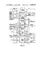
- FIG. 1is a block diagram of packet and circuit switched communications networks in accordance with the invention
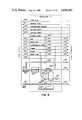
- FIG. 2is a block schematic diagram of a bus controller used in FIG. 1 for controlling the flow of communciations through one of the networks;
- FIG. 3is a block schematic diagram of poll and grant logic circuitry used in the bus controller in FIG. 2;
- FIG. 4is a block schematic diagram of a synchronous cycle counter and generator used in the bus controller in FIG. 2;
- FIG. 5is a block schematic diagram of error checking circuitry used in the bus controller in FIG. 2;
- FIG. 6is a block schematic diagram of one of a plurality of a repeater circuits used in the bus controller in FIG. 2;
- FIG. 7is a block schematic diagrm of one of a plurality of segment bus unit interface circuits used in the communications networks in FIG. 1;
- FIG. 8is an illustration of an address format for communication of packetized data via the communication networks in FIG. 1;
- FIG. 9is an example illustration of bus protocol timing for granting bus access for communication of packetized data in the communication networks in FIG. 1;
- FIG. 10is an example illustration of synchronous bus cycle protocol timing for granting bus access for communication of synchronous data in the communication networks of FIG. 1.
- a Bus Controller A and a Bus Controller Beach include a Main Bus and up to six Repeaters R, each for interfacing the Main Bus with each of up to six Segment Buses A and B respectively.
- An A and B pair of the Segment Buses in each Segmentprovide for connection at up to thirty-two Unit Locations (0-31). All of the buses include multiple conductors providing data leads and address leads which are utilized to carry digital signals in a parallel signal format as well as various control leads. Only those elements being associated with an active one of the netorks A or B are normally in active use at any one time.
- Each of the Segment Busesis terminated remote from its associated Repeater R by a Terminator T.
- Each of the Terminators Tprovide an impedance termination for each of the conductors in the associated Segment Bus and also provides return parity indications for use in the associated bus controller.
- a bus/unit interface circuitis required to provide transmitting and receiving access to the Segment Buses by means of a regimented signal protocol as illustrated in FIGS. 9 and 10 and which is described in more detail in a later portion of the disclosure.
- Each of the bus/unit interface circuitsis identical to the other insofar as it comprises circuitry as exemplified in FIG. 7.
- Each unitis specialized to exclusively perform one of several specific tasks. Examples of some of these tasks are as follows:
- synchronous digital signal service circuitssuch as tone receiver, tone generators, etc., for providing the well-known signalling and supervisory functions required in telephone networks;
- the above-listed tasksare merely illustrative of the various communications services which may be provided with appropriate units by way of the network of FIG. 1.
- One task not mentioned in the listis that of call controlling.
- At least one of the Unit Locations of the networks A and Bis occupied by a call controller Unit.
- the call controller Unitis similar to a central controller in any of various computer controlled switching systems, insofar as it defines communication paths between calling and called ones of the other Units.
- the structure and operation of an exemplary call controller Unit or of any of the other Unitsis neither illustrated nor described in any detail as such is not essential to an understanding of the telecommunication network of the instant invention.
- It is one of the telecommunications networks of FIG. 1which in itself actively provides for inter and intra Unit communications of synchronous and asynchronous digital signals.
- the structure and operation of the networks in FIG. 1is described in more detail with reference to the FIGS. 2-10.
- the Bus Controller in FIG. 2is the source of all timing, control, and address signals which are eventually communicated via ADDRESS and control leads to an associated Segment Bus.
- the Unitsare the sources of all response signals.
- the Units and the Bus Controllerare sources of data information signals communicated via DATA leads.
- a bidirectional microprocessor bus 201is connected between an eight-bit microprocessor 200, a memory 202, an interface circuit 203, a bus switchover circuit 204, a poll and grant circuit 300, a synchronous cycle counter and generator 400 and an error checking circuit 500.
- the memory 202provides permanently stored program instructions defining routines implemented by the microprocessor 200 for configuring operation of the Bus Controller. In this example the microprocessor is an Intel 8031.
- the memory 202also provides temporary storage for use by the microprocessor 200.
- the interface circuit 203provides for data communication between the microprocessor bus 201 and the Units via DATA leads 607 in one of the segment buses as illustrated in FIGS. 6 and 7. In FIG.
- the bus switchover circuit 204includes an input connected to a control lead 219 labelled OTHER USE, and includes an output connected to a control lead 218 labelled USE.
- the OTHER USE lead 219originates with a corresponding output of a bus switchover circuit in the other Bus Controller and the USE lead 218 terminates at a corresponding input of the bus switchover circuit in the other Bus Controller.
- the primary function of the bus switchover circuits 204is that of ultimately controlling which of the Bus Controllers and its associated network is in an active mode of operation and which is in a standby mode of operation.
- the clock generator 205in one example consists of an internal crystal oscillator and phase lock loop circuit, not shown, which generates a clock signal on a CLOCK one of the control leads 217 and a frame signal on a FRAME one of the control leads 216.
- the clock generatoris designed such that it has three distinct modes of operation. The first mode occurs when the Bus Controller is in standby operation, which is indicated by the state of the OTHER USE lead 219. In the first mode the clock generator 205 provides the clock and frame signals being synchronized with corresponding signals produced by a corresponding clock generator in the other Bus Controller. Either of the second and third modes occurs while the Bus Controller is in active opeation.
- the clock and frame signalsare generated in synchronism with timing signals supplied on either of leads SYNCX and SYNCY. These timing signals originate in a remote system and are communicated via one of the Units.
- generation of the clock and frame signalsdepends wholly upon the free running operation of the internal oscillator.
- the null packet generator 206operates substantially as a default data generator such that at times when no other element in the network is actively transmitting on the DATA leads, a null data packet is applied to the buses to prevent the DATA leads from floating. Signal assertions by the null packet generator are carried by the bus 207. Signal assertions by the null packet generator 206 are prevented in the presence of a synchronous cycle flag on a SYNCHRONOUS CYCLE lead 215.
- the poll and grant circuit 300is the source of all addresses for identifying a Unit in the network and is also the source of reset unit signals and the grant flags.
- the addressesare provided on the ADDRESS leads 210 and are thus distributed to each of the Bus Repeaters R and to the error check circuit 500.
- Operational parameterssuch as the range of unit addresses to be polled are determined by the microprocessor 200.
- the moment to moment operation of the poll and grant circuit 300is in response to request flags and done flags generated by the Units and received via REQUEST ones of control leads 221 and DONE ones of the control leads 225.
- the synchronous cycle counter and generator 400defines from the clock and frame signals on the CLOCK and FRAME leads 217 and 216, bus cycle occurrences in frames of bus cycles.
- the microprocessor 200defines a range of bus cycles in which a synchronous transmission request received from a Unit via a SYNCHRONOUS REQUEST one of the control leads 224, may be granted via the SYNCHRONOUS CYCLE lead 215.
- the error check circuit 500monitors signals generated within the Bus Controller and signals generated in the remainder of the network to detect fault occurrences.
- the state of the network as determined by the error check circuit 500is available to the microprocessor 200 via the microprocessor bus 201.
- the error check circuit 500monitors bus cycle counting performed by the sycnchronous cycle counter and generator 400 via a bus 401, addressing performed by the poll and grant circuit 300 via the ADDRESS leads 210, data information on the bus 207, synchronous cycle flags on the SYNCHRONOUS CYCLE lead 215, control parity signals on CONTROL PARITY leads 222, and return parity signals on RETURN PARITY leads 223.
- the control parity and return parity signalsare generated by the Teminator T.
- the error check circuit 500under some detected fault condition generates an abort signal on a lead 501 for controlling operation of the poll and grant circuit 300.
- the poll and grant circuit 300is illustrated in detail in FIG. 3. Circuitry in the upper part of FIG. 3 is primarily concerned with polling Units in the network for service requests being indicated by the request flag. Circuitry in the lower portion of FIG. 3 is primarily concerned with storing and queuing addresses of the various Units which have asserted the request flag and ultimately satisfying each service request.
- addressesare applied to the ADDRESS leads 210 from any of four sources, a poll address register 310, a reset unit address register 314, null address gates 315, and a grant address register 378.
- the poll address register 310asserts an address on the ADDRESS leads 210, each time it is enabled by an address select circuit 320 via a lead 317.
- Addresses for the poll address register 310are generated by a poll address counter 311 which is incremented with each enable occurrence on the lead 317.
- the poll address counter 311generates sequential addresses in a range which is from time to time defined by the microprocessor 200 via the bus 201. One end of the range is stored in a minimum poll address register 313 and the other end of the range is stored in a maximum poll address register and comparator circuit 312.
- the maximum poll address registers and comparator circuit 312In operation each time the address generated in the poll address counter 311 corresponds to the maximum of the range, the maximum poll address registers and comparator circuit 312 generates a load signal which causes the poll address counter 311 to start counting from the minimum address of the range as registered in the minimum poll address register 313.
- the null address gates 315are controlled by the address select circuit 320 via a lead 318 to assert a predetermined null address on the ADDRESS leads 210 during a bus cycle when no other address is asserted to activate the null packet generator 206.
- the reset unit address register 314provides for a Unit reset function wherein the address of the Unit is defined by the microprocessor 200 via the bus 201 and the time at which the Unit is reset is determined by the address select circuit 320 which enables assertion on the ADDRESS leads 210 coincident with generating a reset unit flag on a RESET lead 213 in response to having received a reset request on a lead 321.
- An address parity generator 316responds to each address appearing on the ADDRESS leads 210 by generating parity signals on parity ones of the ADDRESS leads 210.
- the circuitry in the lower portion of FIG. 3is concerned with granting bus cycles to those Units which having been polled have asserted a request flag.
- An address latch 350receives addresses on the ADDRESS leads 210 and passes these addresses via a bus 352, to a first in, first out (FIFO) select circuit 360, to a gateway and disable unit address circuit 354, and to a polling wrap around memory 357.
- FIFOfirst in, first out
- Addresses of both the Gateway Units and disabled ones of the Gateway and Card Unitsare defined by the microprocessor 200 and are received via the bus 201. These addresses are stored in the gateway and disable unit address circuit 354. In the event that an address on the bus 352 corresponds to one of the stored addresses, the gateway and disable unit address circuit 354 asserts a control signal on one of respective leads 355 or 356. Assuming for the moment that the control signal is not asserted, the FIFO select circuit 360 passes the address to a bus 361 and asserts a card FIFO enable signal on a lead 363. This occurs two bus cycles after the address was asserted on the address bus.
- a request flagis received by a request latch 364 via one of the REQUEST leads 221.
- the request flagis received during a bus cycle following the polling incident and a corresponding request control signal is generated on a lead 365 by the request latch 364, two bus cycles following the polling incident.
- a card FIFO 371responds to the signals on the leads 363 and 365 by storing the address from the FIFO select circuit 360. Hence Card Unit addresses are queued for subsequent granting.
- the process described immediately precedingis changed only in that the FIFO select circuit 360 asserts a gate FIFO enable signal on the lead 362, thereby causing the Gateway Unit address to be queued in a gate FIFO 370 in the presence of the request control signal on the lead 365. If on the other hand the address corresponds to that of a Unit having been defined as disabled, gateway and disable unit address circuit 354 asserts a control signal on the lead 356 and neither of the FIFOs, 370 or 371, is selected by the FIFO select circuit 360.
- the polling wrap-around memory 357receives the addresses from the bus 352 and request flag signals on the REQUEST leads 221. In the event that a request flag signal is received, a corresponding memory location is set and is not reset until the same address is again received in the absence of the request flag signal. When the corresponding memory location is set, the polling wrap-around memory asserts a disable signal on a lead 358, which prevents the FIFO select circuit 360 from selecting either of the FIFOs 370 and 371. Hence polling wrap-around which is characterized by more than one appearance of any one address in either of the FIFOs 370 and 371 is prevented.
- Each of the FIFOs 370 and 371include full and empty output ports at which corresponding signals are asserted to indicate the state of each FIFO as being one of full of queued addresses or empty.
- the full portsare wire ORED on a full lead 375 which is connected to an input of the address select circuit 320.
- the empty portsare connected via respective empty leads 372 and 373 inputs of a grant address circuit 380.
- the grant address circuit 380is responsive to grant flags on the GRANT lead 214 to generate output control signals alternately on leads 381 and 382 for causing the respective FIFOs to alternately output previously queued addresses, one after the other, onto a bus 376. If one of the FIFOs is empty only the other FIFO is caused to output the queued addresses.
- Each address appearing on the bus 376is applied to the ADDRESS leads 210 via a grant address register 378 in response to the grant flag.
- the grant address circuitcauses a null address to be asserted on the bus 376 by a null address source 377.
- pollingis halted until sufficient queued addresses are applied to the address bus 210 to provide at least one address space in each of the FIFOs 370 and 371.
- a primary function of the synchronous cycle counter and generator 400, illustrated in FIG. 4,is that of limiting synchronous access to the Data leads 207 so that there is always some failsafe time available for asynchronous communications.
- a Unitmay assert a synchronous request signal two bus cycles prior to a bus cycle having been assigned to it by the call control Unit. Each synchronous request is received via one of the SYNCHRONOUS REQUEST leads 224 and is latched into a synchronous cycle request latch 410 under the control of the clock signals on the CLOCK lead 217.
- One bus cycles later, the state of the synchronous cycle request latch 410is applied at inputs of an AND gate 411 which passes any low signal assertion to an input of an OR gate 412.
- An output of the OR gate 412is the origin of the SYNCHRONOUS CYCLE lead 215.
- the OR gate 412pases the low signal assertion onto the synchronous cycle lead 215 in the event that an output of a comparator 415 is also asserted low.
- a frame latch 413receives the frame signal on the FRAME lead 216 under the control of the clock signal on the CLOCK lead 217 and provides the frame signal at a clear input of a bus cycle counter 414.
- the bus cycle counteris operated by the clock signals on the CLOCK lead 217 to count from its cleared state of zero through to a count of 639 whereupon it is cleared by the delayed frame signal.
- Outputs of the bus cycle counter 414are the origin of the bus 401.
- the bus 401carries ten binary signal bits in parallel for use in the error check circuit 500 and provides the eight highest order binary bits at an input A of the comparator 415.
- Another input B of the comparator 415is connected, via a bus 417, to an output of a maximum cycle register 416.
- the maximum cycle registerstores a maximum cycle number, as defined by the microprocessor 200 via the microprocessor bus 201, beyond which synchronous cycle occurrences are inhibited by the comparator 415.
- the error check circuit 500illustrated in FIG. 5 is primarily concerned with providing information to the microprocessor 200 with respect to various error occurrences in the network.
- the error check circuit 500also generates an abort control signal, for use by the address select circuit 320.
- the DATA leads 207 and RETURN PARITY leads 223are monitored by a check data parity circuit 510.
- the check data parity circuit 510In the event of a parity error in signals on either of the leads 207 and the leads 223, the check data parity circuit 510 generates a parity error signal on a parity error lead 511.
- a packet byte counter 512is initiated at a zero count with each occurrence of the grant flag on the GRANT lead 214.
- the packet byte counter 512counts clock signals on the CLOCK lead 217 and in the event that it reaches a count of 4096 it generates an overflow signal on an OVERFLOW lead 513.
- the overflow signalindicates that a Unit has reached an unexceptable maximum packet length in a single packet transmission.
- Each occurrence of the synchronous cycle signal on the SYNCHRONOUS CYCLE lead 215inhibits the response of the counter 512 to the instant clock signal on the CLOCK lead 217.
- a multiplexer 516gates the state of the ADDRESS leads 210 to a bus 517 except during an assertion of the synchronous cycle signal on the lead 215 whereupon the instant bus cycle count on the bus 401 is gated to the bus 517.
- a check control parity circuit 518receives parity signals from the Terminator T on the CONTROL PARITY leads 222 and indicates a parity error on a parity error lead 519 in the event that at least one of the signals on the CONTROL PARITY leads 222 is asserted.
- Error registers 515provide for temporary storage of error events as indicated on any of the leads 511, 513 and 519, and also provide for temporary storage of either the transmitting Unit's address or the bus cycle count at the instant of the error. If for example a parity error occurs on the DATA leads 207 during a synchronous cycle, the bus cycle count is stored and made available to the microprocessor 200.
- the address at the time of the last grant flag signal occurrenceis made available to the microprocessor 200.
- an abort circuit 514asserts the abort signal.
- FIG. 6illustrates one of the Repeaters R.
- Each of the Bus Controllers in FIG. 1requires up to six Repeaters R for interfacing its Main Bus with up to six corresponding Segment Buses.
- Each Segment Busincludes leads labelled 221-225 each of which is wire connected to a single lead in a corresponding lead groups 221-225 in the Main Bus of the Bus Controller.
- the leads 209, 213, 214, 215, 218 in the Main Busare coupled via amplifiers 640-644 to corresponding leads in the Segment Bus.
- the leads 216 and 217are coupled via inverting amplifiers 645 and 646 to corresponding leads in the Segment Bus.
- the amplifier coupled leadsare identified with corresponding units and ten digits in combination with the numeral six in the hundred digit position.
- Lower order ones of the ADDRESS leads 210are amplifier coupled via amplifiers 650 to corresponding ADDRESS leads 610 in the Segment Bus.
- the remaining higher order ones of the ADDRESS leads 210are decoded by a decoder 620 such that in the event that these higher order leads are of a signal state combination unique to the particular Repeater R a segment enable signal is asserted on an ENABLE lead 601.
- a data transfer control circuitincludes AND gates 622 and 623, a JK flip-flop 624 and an OR gate 625 and an AND gate 628 connected as shown for controlling operation of receive signal transfer gates 626 and transmit signal transfer gates 627.
- the data transfer control circuitis responsive to a coincident occurrence of the grant flag signal and the segment enable signal in the case of packet transmission for permitting asynchronous signal transmission via the gates 627 to the DATA leads 212 of the main bus.
- a delayed synchronous request on one of the leads 420is used by teh AND gate 628 to gate the synchronous cycle signal to the OR gate 625 to cause signal transmission via the gates 627.
- the gates 626permit receive signal transmission to the DATA leads 612 of the Segment Bus.
- the Segment Bus/Unit interface circuit in FIG. 7is used to provide communication between a Unit and one of the Segment Buses. Two of these interface circuits are required for each Unit, one in connection with the Segment Bus A and the other in connection with the Segment Bus B. Each interface circuit provides for the data information transfer function and address and timing interface requirements for all types of Units be they of a synchronous or of an asynchronous nature.
- a NAND gate 724generates a synchronous request signal on the SYNCHRONOUS REQUEST lead 224 in the Segment Bus in response to coincident occurrences of an advanced cycle match signal on a lead 760 and a synchronous required signal on a lead 761, from the associated Unit.
- a comparator 750is connected to receive a slot number, which is defined by binary bit states in accordance with the physical location of the Segment Bus/Unit interface circuit in the network, and to receive the lower order bits of the address on the ADDRESS leads 610.
- the comparator 750generates an address match signal at its output in response to the slot number and the address being equal in the presence of the segment enable signal on the lead 601.
- the output of the comparator 750is connected as shown to a JK flip-flop 751, an AND gate 752, a NAND gate 753, an OR gate 755 and the inverting transmission gate 741.
- the address match signalis gated via the inverting transmission gate 741 to the lead 766 for use in the associated Unit.
- the JK flip-flop 751provides a timing signal for gating a request signal from the associated Unit via a lead 763, and a NAND gate 721 to the REQUEST lead 221 in the Segment Bus. This timing signal is provided in response to an occurrence of the match signal and occurs coincident with the next occurring pulse of the clock signal as gated to the lead 716.
- Outputs of the gates 752 and 753are connected to J and inverting K inputs of a JK flip-flop 757.
- a Q output of the JK flip-flopprovides a gating signal for gating a done signal from the associated Unit via a lead 762 and a NAND gate 725 to the DONE lead 225 of the Segment Bus.
- the gating signalis also provided from an inverting Q output of the JK flip-flop 757 to an input of an OR gate 758.
- This gating signalis initiated in response to a coincident occurrence of a pulse of the grant flag on the GRANT lead 614 and the address match signal from the comparator 750 at the time of the next following pulse of the clock signal on the lead 716.
- the gating signalis terminated in response to the next occurrence of the grant flag signal at the time of the next following pulse of the clock signal.
- the outputs of the respective NAND gate 721, 724 and 725 in each segment/unit interface circuitare WIRE ORed with those of the other segment/unit interface circuits connected to the segment bus.
- the OR gate 758also includes an input connected to receive a cycle match signal from the associated Unit via lead 764. Either of the gating signals from the JK flip-flop 757 or the cycle match signal from the lead 764 is coupled via the OR gate 758 to an input of an AND gate 723 and to an inverting input of an AND gate 722.
- the AND gates 722 and 723each also include inverting inputs connected to the USE lead 618.
- Receive transmission gates 726are used to couple data information signals from the DATA leads 607, in the Segment Bus to DATA leads 707 for reception by the associated Unit.
- Transmit transmission gates 727are used to couple data information signals from the associated Unit, via the DATA leads 707, to the DATA leads 607.
- the receive transmission gates 726are controlled from an output of the AND gate 722 to be ON in the presence of the use signal on the lead 618 while the output of the OR gate 758 is not asserted, and otherwise to be OFF.
- the transmit transmission gates 727are controlled from an output of the AND gate 723 to be ON in the presence of the use signal while the output of the OR gate 758 is asserted and to otherwise be OFF.
- the RESET UNIT lead 613 of the Segment Busis connected to an input of the OR gate 755, the output of which is connected to a D input of a D type flip-flop 756.
- the occurrence of a pulse of the reset signal coincident with the address match signalcauses the flip-flop 756 to assert a reset signal at its inverting Q output at the moment of the next occurring clock pulse on the CLOCK lead 716.
- the reset signalis coupled to a reset lead 765 via the inverting gate 742 for use in the associated Unit.
- Each of the Units shown in FIG. 1have the ability to transmit and receive asynchronous data information signals via its associated Segment Bus/Unit interface circuit (FIG. 7) and the Segment Bus. Some of these Units may also have the capability of being able to transmit and receive synchronous data information signals. Such capability is required in cases in which the Unit provides a port for a synchronous data stream in for example the T1 TDM format, or provides a port for one or more analog or digital telephone station sets. At least one of the remaining Units is the previously referred to call controller Unit.
- the call controller Unitincludes a processor and program and data memories.
- the call controller Unitis exemplary of various known central processing units, operable in accordance with stored program instructions, for controlling the setting up and tearing down of communication paths or channels in a telephone switching network.
- One suitable processor for this purposeis identified by device code 68000 and is available from Motorola. Of course an appropriate processor input/output interface is required to interface any signal level and timing differences between the processor and the Segment Bus/Unit interface circuit.
- the cynchronous Unitsrequire connection memory, for storing call set up information, supervisory status registers and the like, typical of a communication network port in a TDM telecommunication switching exchange.
- the structures and operations of the various types of the Unitsare not described as such will be apparent to persons of typical skill in the electronic arts pertaining to the structures and operations of digitally controlled TDM switching networks in view of the present disclosure and such communication features as said persons envisage.
- inter and intra Unit communicationsare by way of the DATA leads in the Segment and Main Buses.
- Packetized data communications pertaining to information signals entering and leaving the networkare communicated via the DATA leads between Units having an asynchronous communication capability.
- Synchonous data communicationstake priority over the packetized data communications and exclusively pertain to information signals entering and leaving the network.
- the synchronous data communicationsare always conducted between Units having a synchronous capability by way of the DATA leads.
- Destination identifications for all information signals entering and leaving the networkare assigned by the call controller Unit in response to service rquests from the individual Units.
- Communication between each of the Units and the call controller Unitis by means of asynchronous packetized data which is also transmitted via the DATA leads.
- the call controller Unithas no other facility other than the DATA leads of the A and B Segment Buses for communicating with the other Units and the Main Buses.
- a packetized data formatis illustrated in FIG. 8.
- a data packetconsists of up to 4096 words. Each word consists of eight binary bits plus a parity bit, not shown. The bits of each word are transmitted in parallel on the DATA leads. The words of the data packet are sequentially broadcast one word after the other throughout the telecommunications switching network.
- the first word of the packetincludes a Security bit (7) which when asserted indicates that the packet is a network control packet.
- a Null bit (6)is asserted solely by the Bus Controller to indicate a null packet and it prevents any of the Units from responding to the remainder of the word.
- Destination Module bits (4 - 0)specify which one of networks similar to the network of FIG.
- a Route bit (5)indicates which of up to two possible Inter Module Switch Units is designated for transmission of the data packet in the case where another network is specified by the Destination Module bit.
- the second wordconsists of Destination Unit Number (bits 7 - 0) which corresponds to a data address of the Unit for which the remainder of the words of the packet are intended for reception.
- Any Unit receiving information for transmission in the form of packetized data via the telecommunications switching networkfirst requests service by means of one or more data packets each having a header defining the call controller Unit as the destination of the data packet. Subsequently in response to the service request, the call controller Unit transmits a data packet having a header defining the requesting Unit as its destination. The packet also includes the destination address of the required receiving Unit. Subsequent to this the requesting Unit transmits the information in the form of one or more data packets, each data packet having a header as defined by the call controller Unit. The transmission of each packet is continuous with the possible exception of one or more temporary halts to permit one or more synchronous transmissions from one of more other Units.
- FIG. 9includes eight time related rows which are illustrative of signals and functions as labelled together with bracketed numeric identifications of associated leads in the preceding figures.
- the nature of signals transmitted during each bus cycle on the DATA leadsis exemplified by a row labelled DATA wherein null data is signified by the letter "N”, synchronous data is signified by the letter "S”, and each word of each data packet is indicated by a transmitting unit number followed by the word number in the data packet.
- Addressesare generated for the ADDRESS leads 210 by the poll and grant circuit 300. In this example address 0-191 are generated.
- Synchronous cycle occurrencesare defined by the synchronous cycle signal on the SYNCHRONOUS CYCLE lead 215.
- a request flagis asserted by the Unit, having a hardwired slot number 1, in the bus cycle following the address 1 occurrence.
- the DATA leadsare not immediately available for data packet transmission due to synchronous transmission occurrences the DATA leads are not immediately granted to the Unit 1.
- Addressingcontinues until the DATA leads are available whereupon the address for the Unit 1, to which the DATA leads are granted, occurs simultaneously with the grant flag.
- a Unit of address 5also requests access for a data packet transmission.
- the Unit 1begins a packet transmission of which words one and two are header information consistent with FIG. 8.
- the Unit 1transmits words one through five before being interrupted by a synchronous transmission occurrence. Three bus cycles later the Unit 1 transmits the sixth word and as it has only one word of its packet left to transmit, it generates a done flag on the DONE lead 225. Following yet another interruption by a synchronous transmission the last word of the packet is transmitted from the Unit 1 while at the same time the address for the Unit 5 and the grant flag are provided from the poll and grant circuit 300. The poll and grant circuit 300 immediately resumes polling for requests at address 16 and so on. After yet another synchronous transmission interruption the Unit 5 begins to transmit a data packet.
- the reset unit signalis asserted on the RESET UNIT lead 213 by the poll and grant circuit 300.
- All of the Unitsare capable of asynchronous communications in accordance with the protocol illustrated in FIG. 9, and although not shown include elastic storage queues, for transmission and reception of data packets, and appropriate call supervision and connection memory means.
- FIG. 10the synchronous bus cycle protocol is illustrated.
- FIG. 10includes six time related rows which are illustrative of signals and functions as labelled together with bracketed numeric identification of associated leads in the preceding figures.
- the nature of signals transmitted during each bus cycle on the DATA leadsis exemplified in a row labelled DATA wherein asynchronous data is signified by the letter "P" and synchronous data is signified by a numeric label corresponding to the instant bus cycle.
- the only relationship between the access protocol for packetized data and the synchronous bus cycle protocolis that with each occurrence of a synchronous transmission the packet access protocol is arrested as if time has ceased until synchronous transmission ceases whereupon the packet access protocol resumes exactly where it had left off.
- a frame signal pulseoccurs with a period of one millisecond, during which time eight sub-frames of 640 bus cycles each occur.
- Synchronous cycle requestsoriginate in individual ones of the Units at times of bus cycle occurrences having been defined by the call controller Unit.
- Each synchronous cycle requestoccurs one bus cycle in advance of the moment when a synchronous cycle grant may be provided on the SYNCHRONOUS CYCLE lead 215, after which time, transmission of a single word occurs on the DATA leads.
- the transmitted wordis received only by the Unit specified by the call controller Unit.
- Those of the Units capable of synchronous communication in accordance with the protocol illustrated in FIG. 10also include circuit means for defining the bus cycle occurrences by number somewhat similar in function to the bus cycle counter 414 in FIG. 4, and appropriate supervision and connection memory means for synchronous signal calls.
Landscapes
- Engineering & Computer Science (AREA)
- Computer Networks & Wireless Communication (AREA)
- Signal Processing (AREA)
- Data Exchanges In Wide-Area Networks (AREA)
- Small-Scale Networks (AREA)
- Use Of Switch Circuits For Exchanges And Methods Of Control Of Multiplex Exchanges (AREA)
- Mobile Radio Communication Systems (AREA)
- Transceivers (AREA)
Abstract
Description
Claims (14)
Priority Applications (10)
| Application Number | Priority Date | Filing Date | Title |
|---|---|---|---|
| US06/605,721US4608685A (en) | 1984-04-30 | 1984-04-30 | Packet and circuit switched communications network |
| CA000468853ACA1223325A (en) | 1984-04-30 | 1984-11-28 | Packet and circuit switched communications network |
| EP85302596AEP0160443B1 (en) | 1984-04-30 | 1985-04-12 | Packet and circuit switched communications network |
| AT85302596TATE64674T1 (en) | 1984-04-30 | 1985-04-12 | PACKET AND CIRCUIT COMMUNICATION NETWORK. |
| DE8585302596TDE3583254D1 (en) | 1984-04-30 | 1985-04-12 | PACKAGE AND SWITCH-ON COMMUNICATION NETWORK. |
| JP60091285AJPS60250799A (en) | 1984-04-30 | 1985-04-30 | Electric communication switching circuit network and its operating method |
| BR8502053ABR8502053A (en) | 1984-04-30 | 1985-04-30 | TELECOMMUNICATIONS SWITCHING NETWORK AND OPERATING PROCESS OF THE SAME |
| NZ211931ANZ211931A (en) | 1984-04-30 | 1985-04-30 | Packet and circuit switched network |
| AU41999/85AAU575281B2 (en) | 1984-04-30 | 1985-05-06 | Packet and circuit switched communications network |
| CN85103740.2ACN1004044B (en) | 1984-04-30 | 1985-05-16 | Grouping and circuit switched communications network |
Applications Claiming Priority (2)
| Application Number | Priority Date | Filing Date | Title |
|---|---|---|---|
| US06/605,721US4608685A (en) | 1984-04-30 | 1984-04-30 | Packet and circuit switched communications network |
| CN85103740.2ACN1004044B (en) | 1984-04-30 | 1985-05-16 | Grouping and circuit switched communications network |
Publications (1)
| Publication Number | Publication Date |
|---|---|
| US4608685Atrue US4608685A (en) | 1986-08-26 |
Family
ID=24424918
Family Applications (1)
| Application Number | Title | Priority Date | Filing Date |
|---|---|---|---|
| US06/605,721Expired - LifetimeUS4608685A (en) | 1984-04-30 | 1984-04-30 | Packet and circuit switched communications network |
Country Status (10)
| Country | Link |
|---|---|
| US (1) | US4608685A (en) |
| EP (1) | EP0160443B1 (en) |
| JP (1) | JPS60250799A (en) |
| CN (1) | CN1004044B (en) |
| AT (1) | ATE64674T1 (en) |
| AU (1) | AU575281B2 (en) |
| BR (1) | BR8502053A (en) |
| CA (1) | CA1223325A (en) |
| DE (1) | DE3583254D1 (en) |
| NZ (1) | NZ211931A (en) |
Cited By (64)
| Publication number | Priority date | Publication date | Assignee | Title |
|---|---|---|---|---|
| US4658396A (en)* | 1985-03-11 | 1987-04-14 | Barden Robert A | Redundancy arrangement for a local area network |
| US4718057A (en)* | 1985-08-30 | 1988-01-05 | Advanced Micro Devices, Inc. | Streamlined digital signal processor |
| US4727539A (en)* | 1985-03-27 | 1988-02-23 | Hitachi, Ltd. | Multi-element information transmission system |
| US4788682A (en)* | 1986-09-23 | 1988-11-29 | Northern Telecom Limited | Telephone system adapted to telemarketing |
| US4797875A (en)* | 1985-07-08 | 1989-01-10 | Siemens Aktiengesellschaft | Method for monitoring and controlling the traffic in digital transmission networks |
| US4815128A (en)* | 1986-07-03 | 1989-03-21 | Motorola, Inc. | Gateway system and method for interconnecting telephone calls with a digital voice protected radio network |
| WO1989009446A1 (en)* | 1988-04-01 | 1989-10-05 | Telenet Communications Corporation | Communication processor for a packet-switched network |
| US4920567A (en)* | 1986-07-03 | 1990-04-24 | Motorola, Inc. | Secure telephone terminal |
| US4955019A (en)* | 1987-03-02 | 1990-09-04 | Hitachi, Ltd. | Multimedia information exchanging system and equipment therefor |
| US4962497A (en)* | 1989-09-21 | 1990-10-09 | At&T Bell Laboratories | Building-block architecture of a multi-node circuit-and packet-switching system |
| US4975695A (en)* | 1987-10-01 | 1990-12-04 | Data General Corporation | High speed communication processing system |
| US4994960A (en)* | 1986-01-16 | 1991-02-19 | Jupiter Technology, Inc. | Interrupt system for transmitting interrupt request signal and interrupt vector based upon output of synchronized counters representing selected priority value |
| US5023604A (en)* | 1987-08-24 | 1991-06-11 | Hitachi, Ltd. | Communication system |
| US5084872A (en)* | 1989-06-19 | 1992-01-28 | Alcatel Business Systems | Interface for transmit and receive mode access to the synchronous transmission medium of a distributed switching network |
| US5093827A (en)* | 1989-09-21 | 1992-03-03 | At&T Bell Laboratories | Control architecture of a multi-node circuit- and packet-switching system |
| US5107492A (en)* | 1989-06-19 | 1992-04-21 | Alcatel Business Systems | Method and device for managing access to the transmission medium of a multiservice distributed switching network |
| US5177737A (en)* | 1990-01-02 | 1993-01-05 | At&T Bell Laboratories | Multipurpose bus system |
| US5208806A (en)* | 1989-11-17 | 1993-05-04 | Fujitsu Limited | Isdn terminal equipment operating with circuit switching mode and packet switching mode |
| US5235594A (en)* | 1991-08-09 | 1993-08-10 | Westinghouse Electric Corp. | Time division multiplex voice data bus |
| US5291479A (en)* | 1991-07-16 | 1994-03-01 | Digital Technics, Inc. | Modular user programmable telecommunications system with distributed processing |
| US5440698A (en)* | 1990-11-30 | 1995-08-08 | Xerox Corporation | Arbitration of packet switched busses, including busses for shared memory multiprocessors |
| US5461627A (en)* | 1991-12-24 | 1995-10-24 | Rypinski; Chandos A. | Access protocol for a common channel wireless network |
| US5467351A (en)* | 1994-04-22 | 1995-11-14 | At&T Corp. | Extendible round robin local area hub network |
| US5469438A (en)* | 1994-01-28 | 1995-11-21 | At&T Ipm Corp. | Method of transmitting signals in an extendible local area network |
| US5497370A (en)* | 1988-11-16 | 1996-03-05 | Hitachi, Ltd. | Network system |
| US5515373A (en)* | 1994-01-11 | 1996-05-07 | Apple Computer, Inc. | Telecommunications interface for unified handling of varied analog-derived and digital data streams |
| US5594733A (en)* | 1991-09-10 | 1997-01-14 | U.S. Philips Corporation | Multi-station bus system having means for polling and updating of globally relevant information, in particular a station address, and station for use in such system |
| US5621893A (en)* | 1994-11-22 | 1997-04-15 | Lucent Technologies Inc. | System for expanding ports wherein segment switch selectively associates plurality of hubs coupled to first arbiter and plurality of hubs coupled to second arbiter |
| US5666488A (en)* | 1994-11-22 | 1997-09-09 | Lucent Technologies Inc. | Port expansion network and method for lAN hubs |
| US5668853A (en)* | 1992-09-10 | 1997-09-16 | Northern Telecom Limited | Telecommunications calling feature method and apparatus |
| US5671249A (en)* | 1995-01-30 | 1997-09-23 | Level One Communications, Inc. | Inter-repeater backplane with synchronous/asynchronous dual mode operation |
| US5796966A (en)* | 1993-03-01 | 1998-08-18 | Digital Equipment Corporation | Method and apparatus for dynamically controlling data routes through a network |
| US5838748A (en)* | 1993-02-24 | 1998-11-17 | Star Dynamic Corp. | Communication interface between computer and synchronous digital telephone line employing asynchronous data transmission format and having enhanced reliability |
| US5870566A (en)* | 1994-11-22 | 1999-02-09 | Lucent Technologies, Inc. | Port expansion network and method for lan hubs |
| US6005850A (en)* | 1995-04-21 | 1999-12-21 | Hybrid Networks, Inc. | Hybrid access system with remote device monitoring scheme |
| US6014436A (en)* | 1992-12-18 | 2000-01-11 | Nortel Networks Corporation | Telecommunications answering feature method and apparatus |
| US6112230A (en)* | 1997-04-18 | 2000-08-29 | Alcatel | Communication system for information exchange between master and slave stations using frames having organization, request and communication channels |
| US20020069417A1 (en)* | 2000-08-30 | 2002-06-06 | Avi Kliger | Home network system and method |
| US6442169B1 (en) | 1998-11-20 | 2002-08-27 | Level 3 Communications, Inc. | System and method for bypassing data from egress facilities |
| US6614781B1 (en) | 1998-11-20 | 2003-09-02 | Level 3 Communications, Inc. | Voice over data telecommunications network architecture |
| US20040146049A1 (en)* | 2000-09-11 | 2004-07-29 | Bob Sorrentino | Method and system of managing connections between circuit-switched and packet-switched networks |
| US6771655B1 (en)* | 1998-05-29 | 2004-08-03 | Alcatel Canada Inc. | Method and apparatus for managing data transportation |
| US20050036507A1 (en)* | 2003-08-13 | 2005-02-17 | Hall David R. | Apparatus for Fixing Latency |
| US7093015B2 (en)* | 1998-09-11 | 2006-08-15 | Cirrus Logic, Inc. | Method and apparatus for accessing a wireless computer network communication channel by accessing quiet intervals in network frames |
| US7324635B2 (en) | 2000-05-04 | 2008-01-29 | Telemaze Llc | Branch calling and caller ID based call routing telephone features |
| US20080117929A1 (en)* | 2006-11-20 | 2008-05-22 | Broadcom Corporation | System and method for retransmitting packets over a network of communication channels |
| US20080117919A1 (en)* | 2006-11-20 | 2008-05-22 | Broadcom Corporation | Systems and methods for aggregation of packets for transmission through a communications network |
| US20080130779A1 (en)* | 2006-11-20 | 2008-06-05 | Broadcom Corporation | Apparatus and methods for compensating for signal imbalance in a receiver |
| US20080259957A1 (en)* | 2006-11-20 | 2008-10-23 | Broadcom Corporation | Mac to phy interface apparatus and methods for transmission of packets through a communications network |
| US20080271094A1 (en)* | 2000-08-30 | 2008-10-30 | Broadcom Corporation | Home network system and method |
| US20090279643A1 (en)* | 2008-05-06 | 2009-11-12 | Broadcom Corporation | Unbiased signal-to-noise ratio estimation for receiver having channel estimation error |
| US20100158021A1 (en)* | 2008-12-22 | 2010-06-24 | Broadcom Corporation | Systems and methods for physical layer ("phy") concatenation in a moca network |
| US8213309B2 (en) | 2008-12-22 | 2012-07-03 | Broadcom Corporation | Systems and methods for reducing latency and reservation request overhead in a communications network |
| US8238227B2 (en) | 2008-12-22 | 2012-08-07 | Broadcom Corporation | Systems and methods for providing a MoCA improved performance for short burst packets |
| US8345553B2 (en) | 2007-05-31 | 2013-01-01 | Broadcom Corporation | Apparatus and methods for reduction of transmission delay in a communication network |
| US8514860B2 (en) | 2010-02-23 | 2013-08-20 | Broadcom Corporation | Systems and methods for implementing a high throughput mode for a MoCA device |
| US8553547B2 (en) | 2009-03-30 | 2013-10-08 | Broadcom Corporation | Systems and methods for retransmitting packets over a network of communication channels |
| US8611327B2 (en) | 2010-02-22 | 2013-12-17 | Broadcom Corporation | Method and apparatus for policing a QoS flow in a MoCA 2.0 network |
| US8724485B2 (en) | 2000-08-30 | 2014-05-13 | Broadcom Corporation | Home network system and method |
| US8730798B2 (en) | 2009-05-05 | 2014-05-20 | Broadcom Corporation | Transmitter channel throughput in an information network |
| US8867355B2 (en) | 2009-07-14 | 2014-10-21 | Broadcom Corporation | MoCA multicast handling |
| US8942250B2 (en) | 2009-10-07 | 2015-01-27 | Broadcom Corporation | Systems and methods for providing service (“SRV”) node selection |
| US9112717B2 (en) | 2008-07-31 | 2015-08-18 | Broadcom Corporation | Systems and methods for providing a MoCA power management strategy |
| US9531619B2 (en) | 2009-04-07 | 2016-12-27 | Broadcom Corporation | Channel assessment in an information network |
Families Citing this family (12)
| Publication number | Priority date | Publication date | Assignee | Title |
|---|---|---|---|---|
| CN1003154B (en)* | 1985-02-25 | 1989-01-25 | 国际标准电气公司 | System for providing data services in circuit-switched switches |
| US4719617A (en)* | 1985-02-25 | 1988-01-12 | U.S. Holding Company | Full service voice/data system |
| US4821258A (en)* | 1986-08-06 | 1989-04-11 | American Telephone And Telegraph Company At&T Bell Laboratories | Crosspoint circuitry for data packet space division switches |
| IT1202598B (en)* | 1987-02-27 | 1989-02-09 | Etefin Spa | AUTOMATED CONTROL AND MANAGEMENT SYSTEMS OF DEVICES, EQUIPMENT AND PERIPHERAL UNITS FOR THE SWITCHING AND PROCESSING OF SIGNALS IN GENERAL, IN PARTICULAR OF PHONICS AND / OR OF DATA AND / OR IMAGES |
| EP0400930A3 (en)* | 1989-06-02 | 1992-09-30 | Motorola, Inc. | Realtime redundant operating system |
| KR0180774B1 (en)* | 1995-06-28 | 1999-05-15 | 김주용 | Apparatus and method for transferring packet data |
| GB2315635B (en)* | 1996-07-19 | 2000-10-11 | Ericsson Telefon Ab L M | Dynamic load limiting |
| DE19746750A1 (en)* | 1997-10-23 | 1999-05-12 | Volker Schneck | Strand-shaped sealing tape for insertion in joints of a concrete masonry |
| US7469418B1 (en) | 2002-10-01 | 2008-12-23 | Mirage Networks, Inc. | Deterring network incursion |
| US7506360B1 (en) | 2002-10-01 | 2009-03-17 | Mirage Networks, Inc. | Tracking communication for determining device states |
| US8819285B1 (en) | 2002-10-01 | 2014-08-26 | Trustwave Holdings, Inc. | System and method for managing network communications |
| US12061572B2 (en)* | 2022-02-24 | 2024-08-13 | Sap Se | Data blocking for application platforms |
Citations (6)
| Publication number | Priority date | Publication date | Assignee | Title |
|---|---|---|---|---|
| US3985962A (en)* | 1971-08-13 | 1976-10-12 | International Business Machines Corporation | Method of information transmission with priority scheme in a time-division multiplex communication system comprising a loop line |
| US4154983A (en)* | 1978-03-13 | 1979-05-15 | Bell Telephone Laboratories, Incorporated | Loop carrier system for telecommunication and data services |
| US4251880A (en)* | 1979-07-31 | 1981-02-17 | Bell Telephone Laboratories, Incorporated | Digital loop switch for controlling data information having differing transmission characteristics |
| US4380065A (en)* | 1980-09-29 | 1983-04-12 | Honeywell Information Systems Inc. | Communication multiplexer variable priority scheme |
| GB2131654A (en)* | 1982-12-10 | 1984-06-20 | Western Electric Co | Bus dual communication system |
| US4516239A (en)* | 1982-03-15 | 1985-05-07 | At&T Bell Laboratories | System, apparatus and method for controlling a multiple access data communications system including variable length data packets and fixed length collision-free voice packets |
Family Cites Families (8)
| Publication number | Priority date | Publication date | Assignee | Title |
|---|---|---|---|---|
| CH584488A5 (en)* | 1975-05-05 | 1977-01-31 | Ibm | |
| US4199662A (en)* | 1978-07-17 | 1980-04-22 | Lowe Charles S Jr | Hybrid control of time division multiplexing |
| FI76462C (en)* | 1980-09-29 | 1988-10-10 | Honeywell Inf Systems | KOMMUNIKATIONSMULTIPLEXER MED ETT VARIABELT PRIORITETSSCHEMA. |
| JPS58123258A (en)* | 1982-01-19 | 1983-07-22 | Nippon Telegr & Teleph Corp <Ntt> | Circuit and packet combined exchange system |
| US4455646A (en)* | 1982-08-26 | 1984-06-19 | Richard L. Scully | Pulse code modulated digital automatic exchange |
| EP0122684B1 (en)* | 1983-01-18 | 1988-06-15 | Plessey Overseas Limited | Electronic switching system |
| US4627046A (en)* | 1984-04-26 | 1986-12-02 | Data General Corp. | Programmable feature card |
| US4586175A (en)* | 1984-04-30 | 1986-04-29 | Northern Telecom Limited | Method for operating a packet bus for transmission of asynchronous and pseudo-synchronous signals |
- 1984
- 1984-04-30USUS06/605,721patent/US4608685A/ennot_activeExpired - Lifetime
- 1984-11-28CACA000468853Apatent/CA1223325A/ennot_activeExpired
- 1985
- 1985-04-12ATAT85302596Tpatent/ATE64674T1/ennot_activeIP Right Cessation
- 1985-04-12DEDE8585302596Tpatent/DE3583254D1/ennot_activeExpired - Lifetime
- 1985-04-12EPEP85302596Apatent/EP0160443B1/ennot_activeExpired - Lifetime
- 1985-04-30JPJP60091285Apatent/JPS60250799A/enactiveGranted
- 1985-04-30BRBR8502053Apatent/BR8502053A/enunknown
- 1985-04-30NZNZ211931Apatent/NZ211931A/enunknown
- 1985-05-06AUAU41999/85Apatent/AU575281B2/ennot_activeCeased
- 1985-05-16CNCN85103740.2Apatent/CN1004044B/ennot_activeExpired
Patent Citations (6)
| Publication number | Priority date | Publication date | Assignee | Title |
|---|---|---|---|---|
| US3985962A (en)* | 1971-08-13 | 1976-10-12 | International Business Machines Corporation | Method of information transmission with priority scheme in a time-division multiplex communication system comprising a loop line |
| US4154983A (en)* | 1978-03-13 | 1979-05-15 | Bell Telephone Laboratories, Incorporated | Loop carrier system for telecommunication and data services |
| US4251880A (en)* | 1979-07-31 | 1981-02-17 | Bell Telephone Laboratories, Incorporated | Digital loop switch for controlling data information having differing transmission characteristics |
| US4380065A (en)* | 1980-09-29 | 1983-04-12 | Honeywell Information Systems Inc. | Communication multiplexer variable priority scheme |
| US4516239A (en)* | 1982-03-15 | 1985-05-07 | At&T Bell Laboratories | System, apparatus and method for controlling a multiple access data communications system including variable length data packets and fixed length collision-free voice packets |
| GB2131654A (en)* | 1982-12-10 | 1984-06-20 | Western Electric Co | Bus dual communication system |
Cited By (111)
| Publication number | Priority date | Publication date | Assignee | Title |
|---|---|---|---|---|
| US4658396A (en)* | 1985-03-11 | 1987-04-14 | Barden Robert A | Redundancy arrangement for a local area network |
| US4727539A (en)* | 1985-03-27 | 1988-02-23 | Hitachi, Ltd. | Multi-element information transmission system |
| US4797875A (en)* | 1985-07-08 | 1989-01-10 | Siemens Aktiengesellschaft | Method for monitoring and controlling the traffic in digital transmission networks |
| US4718057A (en)* | 1985-08-30 | 1988-01-05 | Advanced Micro Devices, Inc. | Streamlined digital signal processor |
| US4994960A (en)* | 1986-01-16 | 1991-02-19 | Jupiter Technology, Inc. | Interrupt system for transmitting interrupt request signal and interrupt vector based upon output of synchronized counters representing selected priority value |
| US4815128A (en)* | 1986-07-03 | 1989-03-21 | Motorola, Inc. | Gateway system and method for interconnecting telephone calls with a digital voice protected radio network |
| US4920567A (en)* | 1986-07-03 | 1990-04-24 | Motorola, Inc. | Secure telephone terminal |
| US4788682A (en)* | 1986-09-23 | 1988-11-29 | Northern Telecom Limited | Telephone system adapted to telemarketing |
| US4955019A (en)* | 1987-03-02 | 1990-09-04 | Hitachi, Ltd. | Multimedia information exchanging system and equipment therefor |
| US5023604A (en)* | 1987-08-24 | 1991-06-11 | Hitachi, Ltd. | Communication system |
| US4975695A (en)* | 1987-10-01 | 1990-12-04 | Data General Corporation | High speed communication processing system |
| WO1989009446A1 (en)* | 1988-04-01 | 1989-10-05 | Telenet Communications Corporation | Communication processor for a packet-switched network |
| US4979100A (en)* | 1988-04-01 | 1990-12-18 | Sprint International Communications Corp. | Communication processor for a packet-switched network |
| US5497370A (en)* | 1988-11-16 | 1996-03-05 | Hitachi, Ltd. | Network system |
| US5084872A (en)* | 1989-06-19 | 1992-01-28 | Alcatel Business Systems | Interface for transmit and receive mode access to the synchronous transmission medium of a distributed switching network |
| US5107492A (en)* | 1989-06-19 | 1992-04-21 | Alcatel Business Systems | Method and device for managing access to the transmission medium of a multiservice distributed switching network |
| US5093827A (en)* | 1989-09-21 | 1992-03-03 | At&T Bell Laboratories | Control architecture of a multi-node circuit- and packet-switching system |
| US4962497A (en)* | 1989-09-21 | 1990-10-09 | At&T Bell Laboratories | Building-block architecture of a multi-node circuit-and packet-switching system |
| US5208806A (en)* | 1989-11-17 | 1993-05-04 | Fujitsu Limited | Isdn terminal equipment operating with circuit switching mode and packet switching mode |
| US5177737A (en)* | 1990-01-02 | 1993-01-05 | At&T Bell Laboratories | Multipurpose bus system |
| US5440698A (en)* | 1990-11-30 | 1995-08-08 | Xerox Corporation | Arbitration of packet switched busses, including busses for shared memory multiprocessors |
| US5291479A (en)* | 1991-07-16 | 1994-03-01 | Digital Technics, Inc. | Modular user programmable telecommunications system with distributed processing |
| US5235594A (en)* | 1991-08-09 | 1993-08-10 | Westinghouse Electric Corp. | Time division multiplex voice data bus |
| US5594733A (en)* | 1991-09-10 | 1997-01-14 | U.S. Philips Corporation | Multi-station bus system having means for polling and updating of globally relevant information, in particular a station address, and station for use in such system |
| US5461627A (en)* | 1991-12-24 | 1995-10-24 | Rypinski; Chandos A. | Access protocol for a common channel wireless network |
| US5668853A (en)* | 1992-09-10 | 1997-09-16 | Northern Telecom Limited | Telecommunications calling feature method and apparatus |
| US6014436A (en)* | 1992-12-18 | 2000-01-11 | Nortel Networks Corporation | Telecommunications answering feature method and apparatus |
| US5838748A (en)* | 1993-02-24 | 1998-11-17 | Star Dynamic Corp. | Communication interface between computer and synchronous digital telephone line employing asynchronous data transmission format and having enhanced reliability |
| US5796966A (en)* | 1993-03-01 | 1998-08-18 | Digital Equipment Corporation | Method and apparatus for dynamically controlling data routes through a network |
| US5515373A (en)* | 1994-01-11 | 1996-05-07 | Apple Computer, Inc. | Telecommunications interface for unified handling of varied analog-derived and digital data streams |
| US5469438A (en)* | 1994-01-28 | 1995-11-21 | At&T Ipm Corp. | Method of transmitting signals in an extendible local area network |
| US5467351A (en)* | 1994-04-22 | 1995-11-14 | At&T Corp. | Extendible round robin local area hub network |
| US5666488A (en)* | 1994-11-22 | 1997-09-09 | Lucent Technologies Inc. | Port expansion network and method for lAN hubs |
| US5621893A (en)* | 1994-11-22 | 1997-04-15 | Lucent Technologies Inc. | System for expanding ports wherein segment switch selectively associates plurality of hubs coupled to first arbiter and plurality of hubs coupled to second arbiter |
| US5870566A (en)* | 1994-11-22 | 1999-02-09 | Lucent Technologies, Inc. | Port expansion network and method for lan hubs |
| US5671249A (en)* | 1995-01-30 | 1997-09-23 | Level One Communications, Inc. | Inter-repeater backplane with synchronous/asynchronous dual mode operation |
| US6005850A (en)* | 1995-04-21 | 1999-12-21 | Hybrid Networks, Inc. | Hybrid access system with remote device monitoring scheme |
| US6112230A (en)* | 1997-04-18 | 2000-08-29 | Alcatel | Communication system for information exchange between master and slave stations using frames having organization, request and communication channels |
| US6771655B1 (en)* | 1998-05-29 | 2004-08-03 | Alcatel Canada Inc. | Method and apparatus for managing data transportation |
| US7093015B2 (en)* | 1998-09-11 | 2006-08-15 | Cirrus Logic, Inc. | Method and apparatus for accessing a wireless computer network communication channel by accessing quiet intervals in network frames |
| US8693347B2 (en) | 1998-11-20 | 2014-04-08 | Level 3 Communications, Llc | Voice over data telecommunications network architecture |
| US6614781B1 (en) | 1998-11-20 | 2003-09-02 | Level 3 Communications, Inc. | Voice over data telecommunications network architecture |
| US6442169B1 (en) | 1998-11-20 | 2002-08-27 | Level 3 Communications, Inc. | System and method for bypassing data from egress facilities |
| US8416769B2 (en) | 1998-11-20 | 2013-04-09 | Level 3 Communications, Llc | System and method for bypassing data from egress facilities |
| US8953585B2 (en) | 1998-11-20 | 2015-02-10 | Level 3 Communications, Llc | System and method for bypassing data from egress facilities |
| US7200150B2 (en) | 1998-11-20 | 2007-04-03 | Level 3 Communications, Inc. | System and method for bypassing data from egress facilities |
| US8270421B2 (en) | 1998-11-20 | 2012-09-18 | Level 3 Communications, Llc | Voice over data telecommunications network architecture |
| US8089958B2 (en) | 1998-11-20 | 2012-01-03 | Level 3 Communications, Llc | Voice over data telecommunications network architecture |
| US8085761B2 (en) | 1998-11-20 | 2011-12-27 | Level 3 Communications, Llc | Voice over data telecommunications network architecture |
| US8036214B2 (en) | 1998-11-20 | 2011-10-11 | Level 3 Communications, Llc | Voice over data telecommunications network architecture |
| US7564840B2 (en) | 1998-11-20 | 2009-07-21 | Level 3 Communications, Llc | Voice over data telecommunications network architecture |
| US7587036B2 (en) | 2000-05-04 | 2009-09-08 | Telemaze Llc | Tandem access controller within the public switched telephone network |
| US7764777B2 (en) | 2000-05-04 | 2010-07-27 | Telemaze Llc | Branch calling and caller ID based call routing telephone features |
| US8457113B2 (en) | 2000-05-04 | 2013-06-04 | Telemaze Llc | Branch calling and caller ID based call routing telephone features |
| US8175240B2 (en) | 2000-05-04 | 2012-05-08 | Telemaze Llc | Tandem access controller within the public switched telephone network |
| US8155298B2 (en) | 2000-05-04 | 2012-04-10 | Telemaze Llc | Tandem access controller within the public switched telephone network |
| US8718252B2 (en) | 2000-05-04 | 2014-05-06 | Focal Ip, Llc | Tandem access controller within the public switched telephone network |
| US7324635B2 (en) | 2000-05-04 | 2008-01-29 | Telemaze Llc | Branch calling and caller ID based call routing telephone features |
| US8848894B2 (en) | 2000-05-04 | 2014-09-30 | Focal Ip, Llc | Tandem access controller within the public switched telephone network |
| US9083719B2 (en) | 2000-05-04 | 2015-07-14 | Focal Ip, Llc | Controller for the intelligent interconnection of two communication networks, and method of use for same |
| US9160555B2 (en) | 2000-08-30 | 2015-10-13 | Broadcom Corporation | Home network system and method |
| US20090217325A1 (en)* | 2000-08-30 | 2009-08-27 | Broadcom Corporation | Home network system and method |
| US9094226B2 (en) | 2000-08-30 | 2015-07-28 | Broadcom Corporation | Home network system and method |
| US8761200B2 (en)* | 2000-08-30 | 2014-06-24 | Broadcom Corporation | Home network system and method |
| US8755289B2 (en) | 2000-08-30 | 2014-06-17 | Broadcom Corporation | Home network system and method |
| US8724485B2 (en) | 2000-08-30 | 2014-05-13 | Broadcom Corporation | Home network system and method |
| US20080271094A1 (en)* | 2000-08-30 | 2008-10-30 | Broadcom Corporation | Home network system and method |
| US8174999B2 (en)* | 2000-08-30 | 2012-05-08 | Broadcom Corporation | Home network system and method |
| US20020069417A1 (en)* | 2000-08-30 | 2002-06-06 | Avi Kliger | Home network system and method |
| US9184984B2 (en) | 2000-08-30 | 2015-11-10 | Broadcom Corporation | Network module |
| US7486662B2 (en) | 2000-09-11 | 2009-02-03 | Arbinet-Thexchange, Inc. | Method and system of managing connections between circuit-switched and packet-switched networks |
| US20040146049A1 (en)* | 2000-09-11 | 2004-07-29 | Bob Sorrentino | Method and system of managing connections between circuit-switched and packet-switched networks |
| US7586934B2 (en)* | 2003-08-13 | 2009-09-08 | Intelliserv International Holding, Ltd | Apparatus for fixing latency |
| US20050036507A1 (en)* | 2003-08-13 | 2005-02-17 | Hall David R. | Apparatus for Fixing Latency |
| US8526429B2 (en) | 2006-11-20 | 2013-09-03 | Broadcom Corporation | MAC to PHY interface apparatus and methods for transmission of packets through a communications network |
| US20100254402A1 (en)* | 2006-11-20 | 2010-10-07 | Broadcom Corporation | System and method for retransmitting packets over a network of communication channels |
| US7782850B2 (en) | 2006-11-20 | 2010-08-24 | Broadcom Corporation | MAC to PHY interface apparatus and methods for transmission of packets through a communications network |
| US8358663B2 (en) | 2006-11-20 | 2013-01-22 | Broadcom Corporation | System and method for retransmitting packets over a network of communication channels |
| US9008086B2 (en) | 2006-11-20 | 2015-04-14 | Broadcom Corporation | MAC to PHY interface apparatus and methods for transmission of packets through a communications network |
| US8831028B2 (en) | 2006-11-20 | 2014-09-09 | Broadcom Corporation | System and method for retransmitting packets over a network of communication channels |
| US20080259957A1 (en)* | 2006-11-20 | 2008-10-23 | Broadcom Corporation | Mac to phy interface apparatus and methods for transmission of packets through a communications network |
| US7697522B2 (en) | 2006-11-20 | 2010-04-13 | Broadcom Corporation | Systems and methods for aggregation of packets for transmission through a communications network |
| US8537925B2 (en) | 2006-11-20 | 2013-09-17 | Broadcom Corporation | Apparatus and methods for compensating for signal imbalance in a receiver |
| US20080130779A1 (en)* | 2006-11-20 | 2008-06-05 | Broadcom Corporation | Apparatus and methods for compensating for signal imbalance in a receiver |
| US7742495B2 (en) | 2006-11-20 | 2010-06-22 | Broadcom Corporation | System and method for retransmitting packets over a network of communication channels |
| US20080117929A1 (en)* | 2006-11-20 | 2008-05-22 | Broadcom Corporation | System and method for retransmitting packets over a network of communication channels |
| US8090043B2 (en) | 2006-11-20 | 2012-01-03 | Broadcom Corporation | Apparatus and methods for compensating for signal imbalance in a receiver |
| US20080117919A1 (en)* | 2006-11-20 | 2008-05-22 | Broadcom Corporation | Systems and methods for aggregation of packets for transmission through a communications network |
| US9641456B2 (en) | 2007-05-31 | 2017-05-02 | Avago Technologies General Ip (Singapore) Pte. Ltd. | Apparatus and methods for reduction of transmission delay in a communication network |
| US8345553B2 (en) | 2007-05-31 | 2013-01-01 | Broadcom Corporation | Apparatus and methods for reduction of transmission delay in a communication network |
| US20090279643A1 (en)* | 2008-05-06 | 2009-11-12 | Broadcom Corporation | Unbiased signal-to-noise ratio estimation for receiver having channel estimation error |
| US8098770B2 (en) | 2008-05-06 | 2012-01-17 | Broadcom Corporation | Unbiased signal-to-noise ratio estimation for receiver having channel estimation error |
| US9112717B2 (en) | 2008-07-31 | 2015-08-18 | Broadcom Corporation | Systems and methods for providing a MoCA power management strategy |
| US9807692B2 (en) | 2008-07-31 | 2017-10-31 | Avago Technologies General Ip (Singapore) Pte. Ltd. | Systems and methods for providing power management |
| US8811403B2 (en) | 2008-12-22 | 2014-08-19 | Broadcom Corporation | Systems and methods for physical layer (“PHY”) concatenation in a multimedia over coax alliance network |
| US8238227B2 (en) | 2008-12-22 | 2012-08-07 | Broadcom Corporation | Systems and methods for providing a MoCA improved performance for short burst packets |
| US8213309B2 (en) | 2008-12-22 | 2012-07-03 | Broadcom Corporation | Systems and methods for reducing latency and reservation request overhead in a communications network |
| US20100158021A1 (en)* | 2008-12-22 | 2010-06-24 | Broadcom Corporation | Systems and methods for physical layer ("phy") concatenation in a moca network |
| US8804480B2 (en) | 2008-12-22 | 2014-08-12 | Broadcom Corporation | Systems and methods for providing a MoCA improved performance for short burst packets |
| US8737254B2 (en) | 2008-12-22 | 2014-05-27 | Broadcom Corporation | Systems and methods for reducing reservation request overhead in a communications network |
| US8254413B2 (en) | 2008-12-22 | 2012-08-28 | Broadcom Corporation | Systems and methods for physical layer (“PHY”) concatenation in a multimedia over coax alliance network |
| US8553547B2 (en) | 2009-03-30 | 2013-10-08 | Broadcom Corporation | Systems and methods for retransmitting packets over a network of communication channels |
| US9554177B2 (en) | 2009-03-30 | 2017-01-24 | Broadcom Corporation | Systems and methods for retransmitting packets over a network of communication channels |
| US9531619B2 (en) | 2009-04-07 | 2016-12-27 | Broadcom Corporation | Channel assessment in an information network |
| US8730798B2 (en) | 2009-05-05 | 2014-05-20 | Broadcom Corporation | Transmitter channel throughput in an information network |
| US8867355B2 (en) | 2009-07-14 | 2014-10-21 | Broadcom Corporation | MoCA multicast handling |
| US8942250B2 (en) | 2009-10-07 | 2015-01-27 | Broadcom Corporation | Systems and methods for providing service (“SRV”) node selection |
| US8611327B2 (en) | 2010-02-22 | 2013-12-17 | Broadcom Corporation | Method and apparatus for policing a QoS flow in a MoCA 2.0 network |
| US8942220B2 (en) | 2010-02-22 | 2015-01-27 | Broadcom Corporation | Method and apparatus for policing a flow in a network |
| US8514860B2 (en) | 2010-02-23 | 2013-08-20 | Broadcom Corporation | Systems and methods for implementing a high throughput mode for a MoCA device |
| US8953594B2 (en) | 2010-02-23 | 2015-02-10 | Broadcom Corporation | Systems and methods for increasing preambles |
Also Published As
| Publication number | Publication date |
|---|---|
| CN1004044B (en) | 1989-04-26 |
| NZ211931A (en) | 1989-01-06 |
| ATE64674T1 (en) | 1991-07-15 |
| JPS60250799A (en) | 1985-12-11 |
| JPH0448010B2 (en) | 1992-08-05 |
| EP0160443A2 (en) | 1985-11-06 |
| EP0160443A3 (en) | 1987-09-30 |
| CN85103740A (en) | 1986-11-19 |
| CA1223325A (en) | 1987-06-23 |
| AU575281B2 (en) | 1988-07-21 |
| DE3583254D1 (en) | 1991-07-25 |
| EP0160443B1 (en) | 1991-06-19 |
| AU4199985A (en) | 1985-11-07 |
| BR8502053A (en) | 1985-12-31 |
Similar Documents
| Publication | Publication Date | Title |
|---|---|---|
| US4608685A (en) | Packet and circuit switched communications network | |
| US4383315A (en) | Idle time slot seizure and transmission facilities for loop communication system | |
| US4586175A (en) | Method for operating a packet bus for transmission of asynchronous and pseudo-synchronous signals | |
| EP0203971B1 (en) | Idle period signalling in a packet switching system | |
| US5377189A (en) | Hybrid data communications systems | |
| US4429405A (en) | Method of transmitting information between stations attached to a unidirectional transmission ring | |
| EP0100662B1 (en) | Digital communication system | |
| US5291482A (en) | High bandwidth packet switch | |
| CA1237187A (en) | Wide band integrated services local communication system | |
| JPH0319745B2 (en) | ||
| EP0373161B1 (en) | Switching arrangement and method | |
| US5060241A (en) | Synchronizing system for a private digital exchange connected to an isdn | |
| US4779262A (en) | Connection of subscriber communication network base station to external information network | |
| US4634812A (en) | Method of transferring information between microcomputers in a decentralized process control system, particularly for telephone systems | |
| EP0241622B1 (en) | An efficient transmission mechanism integrating data and non coded information | |
| US6751232B1 (en) | Method and apparatus for communicating data between first and second pairs of transceivers communicating on a common communications link | |
| EP0474698B1 (en) | Hybrid data communications system | |
| Boxall | A digital carrier-concentrator system with elastic traffic capacity | |
| EP0130000A2 (en) | Apparatus and method for controlling access by a plurality of units to a shared facility | |
| CA1173942A (en) | Maintenance processing apparatus for remote port units in a telephone switching system | |
| US20060155901A1 (en) | Bus control arrangement and method | |
| JPH063925B2 (en) | Shared channel access control circuit | |
| JPH0785600B2 (en) | Time division exchange system |
Legal Events
| Date | Code | Title | Description |
|---|---|---|---|
| AS | Assignment | Owner name:BELL-NORTHERN RESEARCH LTD., P.O. BOX 3511 STATION Free format text:ASSIGNMENT OF ASSIGNORS INTEREST.;ASSIGNOR:BNR INC.;REEL/FRAME:004320/0946 Effective date:19840611 Owner name:BNR INC. 685A EAST MIDDLEFIELD ROAD, MOUNTAIN VIEW Free format text:ASSIGNMENT OF ASSIGNORS INTEREST.;ASSIGNORS:JAIN, PREM C.;ENNS, FREDERICK;REEL/FRAME:004320/0945 Effective date:19840523 Owner name:NORTHERN TELECOM LIMITED P.O. BOX 6123 STATION A, Free format text:ASSIGNMENT OF ASSIGNORS INTEREST.;ASSIGNOR:BELL-NORTHERN RESEARCH LTD.;REEL/FRAME:004320/0947 Effective date:19840622 | |
| STCF | Information on status: patent grant | Free format text:PATENTED CASE | |
| FEPP | Fee payment procedure | Free format text:PAYOR NUMBER ASSIGNED (ORIGINAL EVENT CODE: ASPN); ENTITY STATUS OF PATENT OWNER: LARGE ENTITY | |
| REMI | Maintenance fee reminder mailed | ||
| FPAY | Fee payment | Year of fee payment:4 | |
| SULP | Surcharge for late payment | ||
| FEPP | Fee payment procedure | Free format text:PAYER NUMBER DE-ASSIGNED (ORIGINAL EVENT CODE: RMPN); ENTITY STATUS OF PATENT OWNER: LARGE ENTITY Free format text:PAYOR NUMBER ASSIGNED (ORIGINAL EVENT CODE: ASPN); ENTITY STATUS OF PATENT OWNER: LARGE ENTITY | |
| FPAY | Fee payment | Year of fee payment:8 | |
| FPAY | Fee payment | Year of fee payment:12 | |
| AS | Assignment | Owner name:NORTEL NETWORKS CORPORATION, CANADA Free format text:CHANGE OF NAME;ASSIGNOR:NORTHERN TELECOM LIMITED;REEL/FRAME:010567/0001 Effective date:19990429 | |
| AS | Assignment | Owner name:NORTEL NETWORKS LIMITED, CANADA Free format text:CHANGE OF NAME;ASSIGNOR:NORTEL NETWORKS CORPORATION;REEL/FRAME:011195/0706 Effective date:20000830 Owner name:NORTEL NETWORKS LIMITED,CANADA Free format text:CHANGE OF NAME;ASSIGNOR:NORTEL NETWORKS CORPORATION;REEL/FRAME:011195/0706 Effective date:20000830 |