US4607232A - Low voltage amplifier circuit - Google Patents
Low voltage amplifier circuitDownload PDFInfo
- Publication number
- US4607232A US4607232AUS06/718,617US71861785AUS4607232AUS 4607232 AUS4607232 AUS 4607232AUS 71861785 AUS71861785 AUS 71861785AUS 4607232 AUS4607232 AUS 4607232A
- Authority
- US
- United States
- Prior art keywords
- transistors
- pair
- current
- transistor
- electrode
- Prior art date
- Legal status (The legal status is an assumption and is not a legal conclusion. Google has not performed a legal analysis and makes no representation as to the accuracy of the status listed.)
- Expired - Lifetime
Links
Images
Classifications
- H—ELECTRICITY
- H03—ELECTRONIC CIRCUITRY
- H03F—AMPLIFIERS
- H03F3/00—Amplifiers with only discharge tubes or only semiconductor devices as amplifying elements
- H03F3/30—Single-ended push-pull [SEPP] amplifiers; Phase-splitters therefor
- H03F3/3066—Single-ended push-pull [SEPP] amplifiers; Phase-splitters therefor the collectors of complementary power transistors being connected to the output
- H03F3/3067—Single-ended push-pull [SEPP] amplifiers; Phase-splitters therefor the collectors of complementary power transistors being connected to the output with asymmetrical driving of the end stage
- H—ELECTRICITY
- H03—ELECTRONIC CIRCUITRY
- H03F—AMPLIFIERS
- H03F3/00—Amplifiers with only discharge tubes or only semiconductor devices as amplifying elements
- H03F3/45—Differential amplifiers
- H03F3/45071—Differential amplifiers with semiconductor devices only
Definitions
- This inventionrelates generally to amplifier circuits and more particularly to bipolar transistor amplifier circuits adapted to operate with low supply voltages.
- bipolar transistor amplifier circuitswhich are able to operate with relatively low voltage supplies, typically 1.5 volt supplies. Further, since this 1.5 volts is the nominal voltage of the supply, as the supply, typically a dry cell battery, ages the voltage decreases and hence it is generally required to design the circuit so that it operates properly with as little as 1.0 to 1.1 volts.
- One type of amplifier circuitincludes a pair of transistors arranged as a complementary emitter follower output stage; one of such transistors being an NPN transistor and the other a PNP transistor. The emitter electrodes are connected together at an output terminal and the collector electrodes are connected to opposite polarities of a voltage supply.
- An input signalis coupled to the base electrode of a third transistor, the emitter and collector electrodes thereof being connected between the collector and base electrodes of the PNP transistor.
- a diode connected PNP transistorprovides a current source between the collector and base of the NPN transistor. With such arrangement, the supply voltage is normally limited to 2(V CE +V BE ) or 1.8 volts.
- a PNP and an NPN transistorare provided with the collector electrodes connected together at a common output terminal. The emitter of the PNP transistor is connected to the positive polarity of the voltage supply and the emitter electrode of the NPN transistor is connected to the negative potential of the supply.
- a pair of resistorsis connected serially between the base electrodes of the transistors and an input signal is fed to the junction between the pair of resistors.
- an electronic circuitcomprising: a pair of transistors having collector electrodes connected together at an output terminal and emitter electrodes coupled to opposite potentials of a voltage supply; a current source; and, means, responsive to a current produced by the current source, for establishing bias currents to base electrodes of the pair of transistors in accordance with an input signal, such bias currents being dependent on the current produced by the current source and being substantially independent, over a nominal operating supply voltage range of the circuit, of variations in the voltage supply.
- a resistoris coupled between the voltage supply and an emitter of one of the pair of transistors. With such arrangement current gain is provided. Further, the supply voltage may be as low as 2V CE (SAT)+IR where IR is the voltage drop across the resistor, typically 30 millivolts. Hence, the minimum supply voltage is still less than one volt.
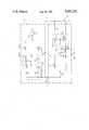
- FIGUREis a schematic diagram of an amplifier circuit according to the invention.
- an amplifier circuit 10having an emitter coupled differential amplifier section 12 driving a load 13 through an output stage 14.
- the differential amplifier section 12includes a pair of PNP transistors, Q 1 , Q 2 , having emitter electrodes connected to the positive potential, +V, of a voltage supply through a constant current source 16.
- the base electrodes of the transistors Q 1 , Q 2are coupled to a pair of input terminals 18, 20, respectively, as shown.
- the collector electrodes of transistors Q 1 , Q 2are connected to a current mirror 22. More particularly, the input 24 to the current mirror 22 is connected to the collector electrode of transistor Q 1 and the output 28 of such current mirror 22 is connected to the collector electrode of transistor Q 2 and also to the output stage 14 via line 23, as shown.
- Current mirror 22thus includes a diode connected transistor Q 3 having the base and collector electrodes thereof connected together and to input 24 and having the emitter connected to the negative potential, -V, of the voltage supply through a resistor R 1 .
- the portion of the current I ohere 15 to 20 microamps
- current source 16 passing through transistor Q 1 to input 24 of the current mirror 22is mirrored by the current mirror 22 into a substantially equal current into the collector of transistor Q 4 .
- the output stage 14includes a pair of output transistors Q 5 , Q 6 having the emitter and collector electrodes thereof serially coupled between the positive and negative potentials of the voltage supply.
- transistor Q 5here a PNP transistor, has its emitter electrode connected to the +V potential of the voltage supply and its collector electrode connected together with the collector electrode of transistor Q 6 at output terminal 32.
- the emitter electrode of transistor Q 6is coupled to the negative -V potential of the voltage supply through a resistor R 3 , here R 3 is 187 ohms.
- Transistor Q 5is part of a current mirror 34, such current mirror 34 including a diode connected transistor Q 7 .
- the emitter electrode of transistor Q 7is coupled to +V through a resistor R 4 , here 25K ohms.
- the base electrodes of transistors Q 5 , Q 7are connected together and to the collector electrode of transistor Q 7 , as shown.
- the emitter area of transistor Q 5is, here 25 times greater than the emitter area of transistor Q 7 .
- Capacitor C 2(here 33 pica farads) is connected between the base and collector electrodes of transistor Q 6 and such capacitor C 2 , along with capacitor C 1 (here 220 pica farads), provide high frequency stabilization for the circuit 10.
- the collector of transistor Q 7is connected to the emitter of transistor Q 8 .
- the collector of transistor Q 8is coupled to the negative potential -V of the voltage supply through a resistor R 3 , as shown.
- the inputs to the output stage 14, i.e., lines 23, 30,are coupled to the base electrodes of transistors Q 6 , Q 8 , respectively, as shown.
- the emitter area of transistor Q 8is here twice the emitter area of transistor Q 7 and the emitter area of transistor Q 6 is here four times larger than the emitter area of transistor Q 7 .
- the current I a through R 3is insufficient to bias transistor Q 8 off. Further, because the 25 to 1 emitter area ratio of transistors Q 5 , Q 7 , a current 25I a (or greater because of resistor R 4 , here 25K ohms) passes to load 13 with the voltage at terminal 32 going positive. On the other hand, when the voltage at the base electrode of transistor Q 1 is more positive than the voltage at the base of transistor Q 2 , the current through the collector of transistor Q 2 is greater than the current through the collector of transistor Q 1 . Further, since the current mirror 22 draws through the collector of transistor Q 4 , a current equal to the current through the collector of transistor Q 1 , the excess current passes into the base of transistor Q 6 .
- resistor R 3increases the current gain because for a fixed bias current to the base of transistor Q 6 , transistor Q 6 will draw a predetermined amount of collector current. Since transistor Q 5 is substantially non-conducting, this required collector current must come from the load 13. To put it another way, in the absence of resistor R 3 for this fixed bias current into the base of transistor Q 6 , the required collector current would be made up of some portion coming from transistor Q 5 as well as from the load 13.
- transistor Q 6With resistor R 3 biasing towards non-conduction transistor Q 5 , transistor Q 6 (for this fixed current into its base) draws more current from the load 13 than if transistor Q 5 were in a more conducting condition. The effect then of resistor R 3 is to increase the current gain of the output stage 14. Gain is provided when current is passed to the load 13 from transistor Q 5 because such transistor is controlled by the voltage at its base electrode from mirror 22.
- transistor Q 6may be considered as a common emitter stage and transistor Q 8 , a common base stage.
- the maximum voltage across resistor R 3is 30 to 40 mV.
- the voltage supply between +V and -Vmay be as little as 1.0 volt.
- bias currents to the base electrodes of transistors Q 6 , Q 8are dependent on the constant current source 16 and hence are, over the nominal supply voltage operating range, independent of the supply voltage. Further, since the bias current to the base of transistor Q 5 is controlled by the base bias current to transistor Q 8 , it follows that the bias current to the base of transistor Q 5 is also dependent on the current produced by the current source 16 and is substantially independent, over a nominal supply voltage operating range, on variations in the supply voltage.
Landscapes
- Engineering & Computer Science (AREA)
- Power Engineering (AREA)
- Amplifiers (AREA)
Abstract
Description
Claims (12)
Priority Applications (2)
| Application Number | Priority Date | Filing Date | Title |
|---|---|---|---|
| US06/718,617US4607232A (en) | 1985-04-01 | 1985-04-01 | Low voltage amplifier circuit |
| JP61075397AJPS61230411A (en) | 1985-04-01 | 1986-04-01 | Electric circuit |
Applications Claiming Priority (1)
| Application Number | Priority Date | Filing Date | Title |
|---|---|---|---|
| US06/718,617US4607232A (en) | 1985-04-01 | 1985-04-01 | Low voltage amplifier circuit |
Publications (1)
| Publication Number | Publication Date |
|---|---|
| US4607232Atrue US4607232A (en) | 1986-08-19 |
Family
ID=24886783
Family Applications (1)
| Application Number | Title | Priority Date | Filing Date |
|---|---|---|---|
| US06/718,617Expired - LifetimeUS4607232A (en) | 1985-04-01 | 1985-04-01 | Low voltage amplifier circuit |
Country Status (2)
| Country | Link |
|---|---|
| US (1) | US4607232A (en) |
| JP (1) | JPS61230411A (en) |
Cited By (29)
| Publication number | Priority date | Publication date | Assignee | Title |
|---|---|---|---|---|
| US4710728A (en)* | 1986-06-30 | 1987-12-01 | Motorola, Inc. | Amplifier having improved gain-bandwidth product |
| US4717869A (en)* | 1985-09-02 | 1988-01-05 | Siemens Aktiengesellschaft | Controlled current source apparatus for signals of either polarity |
| US4901030A (en)* | 1987-09-14 | 1990-02-13 | Gennum Corporation | Operational amplifier stages |
| US4902795A (en)* | 1986-01-15 | 1990-02-20 | Bayer Aktiengesellschaft | Intermediates for 1,8-bridged 4-quinolone-3-carboxylic acid antibacterials |
| US4941153A (en)* | 1987-08-25 | 1990-07-10 | Hughes Aircraft Company | High-speed digital data communication system |
| EP0384710A1 (en)* | 1989-02-20 | 1990-08-29 | Kabushiki Kaisha Toshiba | Amplifier circuit operable at low power source voltage |
| US5401995A (en)* | 1992-07-31 | 1995-03-28 | Sgs-Thomson Microelectronics, S.R.L. | Circuit with diode-protected emitter resistors |
| EP0619646A3 (en)* | 1993-04-07 | 1996-02-07 | Philips Patentverwaltung | Amplifier arrangement. |
| WO1996016475A1 (en)* | 1994-11-22 | 1996-05-30 | Resound Corporation | Improved class ab amplifier |
| US5745587A (en)* | 1995-06-07 | 1998-04-28 | Bausch & Lomb Incorporated | Hearing aid amplifier circuitry |
| US6020768A (en)* | 1998-05-13 | 2000-02-01 | Oak Technology, Inc. | CMOS low-voltage comparator |
| US6094098A (en)* | 1998-06-17 | 2000-07-25 | Lucent Technologies Inc. | Technique for designing an amplifier circuit in an integrated circuit device |
| US6137361A (en)* | 1999-02-03 | 2000-10-24 | National Semiconductor Corporation | Low power class A amplifier circuit |
| US20030231063A1 (en)* | 2002-06-17 | 2003-12-18 | Stmicroelectronics S.R.L. | Device for converting a differential signal to a single signal |
| US20060028248A1 (en)* | 2004-08-06 | 2006-02-09 | Atmel Germany Gmbh | Voltage comparator |
| US20060173724A1 (en)* | 2005-01-28 | 2006-08-03 | Pegasystems, Inc. | Methods and apparatus for work management and routing |
| US20070170989A1 (en)* | 2006-01-24 | 2007-07-26 | Meng-An Pan | Analog amplitude detector |
| US8250525B2 (en) | 2007-03-02 | 2012-08-21 | Pegasystems Inc. | Proactive performance management for multi-user enterprise software systems |
| US8479157B2 (en) | 2004-05-26 | 2013-07-02 | Pegasystems Inc. | Methods and apparatus for integration of declarative rule-based processing with procedural programming in a digital data-processing evironment |
| US8880487B1 (en) | 2011-02-18 | 2014-11-04 | Pegasystems Inc. | Systems and methods for distributed rules processing |
| US8924335B1 (en) | 2006-03-30 | 2014-12-30 | Pegasystems Inc. | Rule-based user interface conformance methods |
| US9195936B1 (en) | 2011-12-30 | 2015-11-24 | Pegasystems Inc. | System and method for updating or modifying an application without manual coding |
| US9678719B1 (en) | 2009-03-30 | 2017-06-13 | Pegasystems Inc. | System and software for creation and modification of software |
| US10469396B2 (en) | 2014-10-10 | 2019-11-05 | Pegasystems, Inc. | Event processing with enhanced throughput |
| US10467200B1 (en) | 2009-03-12 | 2019-11-05 | Pegasystems, Inc. | Techniques for dynamic data processing |
| US10698599B2 (en) | 2016-06-03 | 2020-06-30 | Pegasystems, Inc. | Connecting graphical shapes using gestures |
| US10698647B2 (en) | 2016-07-11 | 2020-06-30 | Pegasystems Inc. | Selective sharing for collaborative application usage |
| US11048488B2 (en) | 2018-08-14 | 2021-06-29 | Pegasystems, Inc. | Software code optimizer and method |
| US11567945B1 (en) | 2020-08-27 | 2023-01-31 | Pegasystems Inc. | Customized digital content generation systems and methods |
Citations (1)
| Publication number | Priority date | Publication date | Assignee | Title |
|---|---|---|---|---|
| US4267519A (en)* | 1979-09-18 | 1981-05-12 | Rca Corporation | Operational transconductance amplifiers with non-linear component current amplifiers |
Family Cites Families (2)
| Publication number | Priority date | Publication date | Assignee | Title |
|---|---|---|---|---|
| JPS5894212A (en)* | 1981-11-30 | 1983-06-04 | Matsushita Electric Ind Co Ltd | Constant current output circuit |
| JPS5939109A (en)* | 1982-08-27 | 1984-03-03 | Matsushita Electric Ind Co Ltd | Current output amplifier |
- 1985
- 1985-04-01USUS06/718,617patent/US4607232A/ennot_activeExpired - Lifetime
- 1986
- 1986-04-01JPJP61075397Apatent/JPS61230411A/enactivePending
Patent Citations (1)
| Publication number | Priority date | Publication date | Assignee | Title |
|---|---|---|---|---|
| US4267519A (en)* | 1979-09-18 | 1981-05-12 | Rca Corporation | Operational transconductance amplifiers with non-linear component current amplifiers |
Cited By (41)
| Publication number | Priority date | Publication date | Assignee | Title |
|---|---|---|---|---|
| US4717869A (en)* | 1985-09-02 | 1988-01-05 | Siemens Aktiengesellschaft | Controlled current source apparatus for signals of either polarity |
| US4902795A (en)* | 1986-01-15 | 1990-02-20 | Bayer Aktiengesellschaft | Intermediates for 1,8-bridged 4-quinolone-3-carboxylic acid antibacterials |
| US4977263A (en)* | 1986-01-15 | 1990-12-11 | Bayer Aktiengesellschaft | Process for preparing 1,8-bridged 4-quinolone-3-carboxylic acid antibacterials |
| US4710728A (en)* | 1986-06-30 | 1987-12-01 | Motorola, Inc. | Amplifier having improved gain-bandwidth product |
| US4941153A (en)* | 1987-08-25 | 1990-07-10 | Hughes Aircraft Company | High-speed digital data communication system |
| US4901030A (en)* | 1987-09-14 | 1990-02-13 | Gennum Corporation | Operational amplifier stages |
| EP0384710A1 (en)* | 1989-02-20 | 1990-08-29 | Kabushiki Kaisha Toshiba | Amplifier circuit operable at low power source voltage |
| US5401995A (en)* | 1992-07-31 | 1995-03-28 | Sgs-Thomson Microelectronics, S.R.L. | Circuit with diode-protected emitter resistors |
| EP0619646A3 (en)* | 1993-04-07 | 1996-02-07 | Philips Patentverwaltung | Amplifier arrangement. |
| WO1996016475A1 (en)* | 1994-11-22 | 1996-05-30 | Resound Corporation | Improved class ab amplifier |
| US5745587A (en)* | 1995-06-07 | 1998-04-28 | Bausch & Lomb Incorporated | Hearing aid amplifier circuitry |
| US6020768A (en)* | 1998-05-13 | 2000-02-01 | Oak Technology, Inc. | CMOS low-voltage comparator |
| US6094098A (en)* | 1998-06-17 | 2000-07-25 | Lucent Technologies Inc. | Technique for designing an amplifier circuit in an integrated circuit device |
| US6137361A (en)* | 1999-02-03 | 2000-10-24 | National Semiconductor Corporation | Low power class A amplifier circuit |
| US20030231063A1 (en)* | 2002-06-17 | 2003-12-18 | Stmicroelectronics S.R.L. | Device for converting a differential signal to a single signal |
| US6909328B2 (en)* | 2002-06-17 | 2005-06-21 | Stmicroelectronics S.R.L. | Device for converting a differential signal to a single signal |
| US8959480B2 (en) | 2004-05-26 | 2015-02-17 | Pegasystems Inc. | Methods and apparatus for integration of declarative rule-based processing with procedural programming in a digital data-processing environment |
| US8479157B2 (en) | 2004-05-26 | 2013-07-02 | Pegasystems Inc. | Methods and apparatus for integration of declarative rule-based processing with procedural programming in a digital data-processing evironment |
| US7626427B2 (en)* | 2004-08-06 | 2009-12-01 | Atmel Automotive Gmbh | Voltage comparator utilizing voltage to current conversion |
| US20060028248A1 (en)* | 2004-08-06 | 2006-02-09 | Atmel Germany Gmbh | Voltage comparator |
| US8335704B2 (en) | 2005-01-28 | 2012-12-18 | Pegasystems Inc. | Methods and apparatus for work management and routing |
| US20060173724A1 (en)* | 2005-01-28 | 2006-08-03 | Pegasystems, Inc. | Methods and apparatus for work management and routing |
| US20070170989A1 (en)* | 2006-01-24 | 2007-07-26 | Meng-An Pan | Analog amplitude detector |
| US7336129B2 (en)* | 2006-01-24 | 2008-02-26 | Broadcom Corporation | Analog amplitude detector |
| US10838569B2 (en) | 2006-03-30 | 2020-11-17 | Pegasystems Inc. | Method and apparatus for user interface non-conformance detection and correction |
| US8924335B1 (en) | 2006-03-30 | 2014-12-30 | Pegasystems Inc. | Rule-based user interface conformance methods |
| US9658735B2 (en) | 2006-03-30 | 2017-05-23 | Pegasystems Inc. | Methods and apparatus for user interface optimization |
| US8250525B2 (en) | 2007-03-02 | 2012-08-21 | Pegasystems Inc. | Proactive performance management for multi-user enterprise software systems |
| US9189361B2 (en) | 2007-03-02 | 2015-11-17 | Pegasystems Inc. | Proactive performance management for multi-user enterprise software systems |
| US10467200B1 (en) | 2009-03-12 | 2019-11-05 | Pegasystems, Inc. | Techniques for dynamic data processing |
| US9678719B1 (en) | 2009-03-30 | 2017-06-13 | Pegasystems Inc. | System and software for creation and modification of software |
| US9270743B2 (en) | 2011-02-18 | 2016-02-23 | Pegasystems Inc. | Systems and methods for distributed rules processing |
| US8880487B1 (en) | 2011-02-18 | 2014-11-04 | Pegasystems Inc. | Systems and methods for distributed rules processing |
| US9195936B1 (en) | 2011-12-30 | 2015-11-24 | Pegasystems Inc. | System and method for updating or modifying an application without manual coding |
| US10572236B2 (en) | 2011-12-30 | 2020-02-25 | Pegasystems, Inc. | System and method for updating or modifying an application without manual coding |
| US10469396B2 (en) | 2014-10-10 | 2019-11-05 | Pegasystems, Inc. | Event processing with enhanced throughput |
| US11057313B2 (en) | 2014-10-10 | 2021-07-06 | Pegasystems Inc. | Event processing with enhanced throughput |
| US10698599B2 (en) | 2016-06-03 | 2020-06-30 | Pegasystems, Inc. | Connecting graphical shapes using gestures |
| US10698647B2 (en) | 2016-07-11 | 2020-06-30 | Pegasystems Inc. | Selective sharing for collaborative application usage |
| US11048488B2 (en) | 2018-08-14 | 2021-06-29 | Pegasystems, Inc. | Software code optimizer and method |
| US11567945B1 (en) | 2020-08-27 | 2023-01-31 | Pegasystems Inc. | Customized digital content generation systems and methods |
Also Published As
| Publication number | Publication date |
|---|---|
| JPS61230411A (en) | 1986-10-14 |
Similar Documents
| Publication | Publication Date | Title |
|---|---|---|
| US4607232A (en) | Low voltage amplifier circuit | |
| US4808907A (en) | Current regulator and method | |
| US3648154A (en) | Power supply start circuit and amplifier circuit | |
| US4437023A (en) | Current mirror source circuitry | |
| US4837523A (en) | High slew rate linear amplifier | |
| US4591804A (en) | Cascode current-source arrangement having dual current paths | |
| US4237414A (en) | High impedance output current source | |
| US4517476A (en) | ECL Gate having emitter bias current switched by input signal | |
| US4602172A (en) | High input impedance circuit | |
| US4922208A (en) | Output stage for an operational amplifier | |
| US4454479A (en) | Operational amplifier with improved output capability | |
| US4194166A (en) | Differential amplifier with a current mirror circuit | |
| US4779059A (en) | Current mirror circuit | |
| US6114904A (en) | Fast amplifier output stage | |
| KR900000482B1 (en) | Current meter circuit | |
| KR920009548B1 (en) | Current source device | |
| US4122402A (en) | Buffer amplifier circuit suitable for manufacture in monolithic integrated circuit form | |
| US4937515A (en) | Low supply voltage current mirror circuit | |
| US4005371A (en) | Bias circuit for differential amplifier | |
| US3942129A (en) | Controlled gain amplifier | |
| US4910425A (en) | Input buffer circuit | |
| US4103220A (en) | Low dissipation voltage regulator | |
| US5343165A (en) | Amplifier having a symmetrical output characteristic | |
| US4910477A (en) | Bridge-type linear amplifier with wide dynamic range and high efficiency | |
| US4553107A (en) | Current mirror circuit having stabilized output current |
Legal Events
| Date | Code | Title | Description |
|---|---|---|---|
| AS | Assignment | Owner name:RAYTHEON COMPANY, LEXINGTON, MA 02173 A CORP OF DE Free format text:ASSIGNMENT OF ASSIGNORS INTEREST.;ASSIGNOR:GILL, HARRY A. JR.;REEL/FRAME:004391/0601 Effective date:19850328 | |
| STCF | Information on status: patent grant | Free format text:PATENTED CASE | |
| FEPP | Fee payment procedure | Free format text:PAYOR NUMBER ASSIGNED (ORIGINAL EVENT CODE: ASPN); ENTITY STATUS OF PATENT OWNER: LARGE ENTITY | |
| FPAY | Fee payment | Year of fee payment:4 | |
| FPAY | Fee payment | Year of fee payment:8 | |
| FPAY | Fee payment | Year of fee payment:12 | |
| AS | Assignment | Owner name:FAIRCHILD SEMICONDUCTOR, MAINE Free format text:ASSIGNMENT OF ASSIGNORS INTEREST;ASSIGNOR:RAYTHEON COMPANY;REEL/FRAME:009342/0773 Effective date:19980615 | |
| AS | Assignment | Owner name:CREDIT SUISSE FIRST BOSTON, NEW YORK Free format text:SECURITY AGREEMENT;ASSIGNOR:FAIRCHILD SEMICONDUCTOR CORPORATION;REEL/FRAME:009883/0800 Effective date:19990414 | |
| AS | Assignment | Owner name:FAIRCHILD SEMICONDUCTOR CORPORATION, MAINE Free format text:RELEASE BY SECURED PARTY;ASSIGNOR:BANKERS TRUST COMPANY;REEL/FRAME:009901/0528 Effective date:19990414 | |
| AS | Assignment | Owner name:FAIRCHILD SEMICONDUCTOR CORPORATION, MAINE Free format text:RELEASE;ASSIGNOR:CREDIT SUISSE FIRST BOSTON;REEL/FRAME:010996/0537 Effective date:20000602 |