US4600932A - Enhanced mobility buried channel transistor structure - Google Patents
Enhanced mobility buried channel transistor structureDownload PDFInfo
- Publication number
- US4600932A US4600932AUS06/660,175US66017584AUS4600932AUS 4600932 AUS4600932 AUS 4600932AUS 66017584 AUS66017584 AUS 66017584AUS 4600932 AUS4600932 AUS 4600932A
- Authority
- US
- United States
- Prior art keywords
- layer
- undoped
- doped
- deposited onto
- deposited
- Prior art date
- Legal status (The legal status is an assumption and is not a legal conclusion. Google has not performed a legal analysis and makes no representation as to the accuracy of the status listed.)
- Expired - Lifetime
Links
- 229910001218Gallium arsenideInorganic materials0.000claimsabstractdescription34
- JBRZTFJDHDCESZ-UHFFFAOYSA-NAsGaChemical compound[As]#[Ga]JBRZTFJDHDCESZ-UHFFFAOYSA-N0.000claimsdescription33
- 150000001875compoundsChemical class0.000claimsdescription16
- 239000000758substrateSubstances0.000claimsdescription15
- 230000000737periodic effectEffects0.000claimsdescription2
- 230000037230mobilityEffects0.000description29
- 239000000463materialSubstances0.000description12
- 229910052782aluminiumInorganic materials0.000description6
- XAGFODPZIPBFFR-UHFFFAOYSA-NaluminiumChemical compound[Al]XAGFODPZIPBFFR-UHFFFAOYSA-N0.000description6
- 239000012535impuritySubstances0.000description5
- 230000003993interactionEffects0.000description5
- 230000005669field effectEffects0.000description4
- 239000004065semiconductorSubstances0.000description4
- 239000002019doping agentSubstances0.000description3
- 239000012212insulatorSubstances0.000description3
- 238000001451molecular beam epitaxyMethods0.000description3
- 229910000980Aluminium gallium arsenideInorganic materials0.000description2
- 239000000969carrierSubstances0.000description2
- 238000004519manufacturing processMethods0.000description2
- 230000005533two-dimensional electron gasEffects0.000description2
- 239000004020conductorSubstances0.000description1
- 238000010276constructionMethods0.000description1
- 230000001419dependent effectEffects0.000description1
- 238000010586diagramMethods0.000description1
- 239000003574free electronSubstances0.000description1
- 238000000034methodMethods0.000description1
- 238000012986modificationMethods0.000description1
- 230000004048modificationEffects0.000description1
- 238000005381potential energyMethods0.000description1
- 238000000926separation methodMethods0.000description1
- 229910052710siliconInorganic materials0.000description1
- 239000010703siliconSubstances0.000description1
- 239000007787solidSubstances0.000description1
- 239000000126substanceSubstances0.000description1
- 239000013589supplementSubstances0.000description1
Images

Classifications
- H—ELECTRICITY
- H10—SEMICONDUCTOR DEVICES; ELECTRIC SOLID-STATE DEVICES NOT OTHERWISE PROVIDED FOR
- H10D—INORGANIC ELECTRIC SEMICONDUCTOR DEVICES
- H10D30/00—Field-effect transistors [FET]
- H10D30/40—FETs having zero-dimensional [0D], one-dimensional [1D] or two-dimensional [2D] charge carrier gas channels
- H10D30/47—FETs having zero-dimensional [0D], one-dimensional [1D] or two-dimensional [2D] charge carrier gas channels having 2D charge carrier gas channels, e.g. nanoribbon FETs or high electron mobility transistors [HEMT]
- H10D30/471—High electron mobility transistors [HEMT] or high hole mobility transistors [HHMT]
- H10D30/475—High electron mobility transistors [HEMT] or high hole mobility transistors [HHMT] having wider bandgap layer formed on top of lower bandgap active layer, e.g. undoped barrier HEMTs such as i-AlGaN/GaN HEMTs
- H10D30/4755—High electron mobility transistors [HEMT] or high hole mobility transistors [HHMT] having wider bandgap layer formed on top of lower bandgap active layer, e.g. undoped barrier HEMTs such as i-AlGaN/GaN HEMTs having wide bandgap charge-carrier supplying layers, e.g. modulation doped HEMTs such as n-AlGaAs/GaAs HEMTs
Definitions
- This inventionrelates to enhanced, mobility buried channel transistor structures. Accordingly, it is a general object of this invention to provide new and improved structures of such character.
- Enhanced mobility devices using Al x Ga 1-x As/GaAs materials systemshave been reported upon by others and their potential use as high-speed active devices have been recognized.
- Mimura et al.in an article entitled "A New Field-Effect Transistor with Selectively Doped GaAs/n-Al x Ga 1-x As Heterojunctions", Japanese Journal of Applied Physics, Vol. 19, No. 5, May, 1980, pp. 1225-1227, describe studies of field-effect control of high mobility electrons in MBE (molecular beam epitaxy)grown selectively doped GaAs/n-Al x Ga 1-x As heterojunctions.
- MBEmolecular beam epitaxy
- HEMThigh electron mobility transistor
- heterostructure junctionsincluding alternate layers of GaAs and Al x Ga 1-x As, with Al x Ga 1-x As layers being selectively doped with silicon, due to higher electron affinity of GaAs, free electrons in the Al x Ga 1-x As layers are transferred to the non-doped GaAs layers where they form a quasi two-dimensional Fermi gas.
- the mobility enhancement behavioris attributed to the spatial separation between the electrons and their parent donor impurities.
- a basic enhanced mobility transistor structureincludes a semi-insulating substrate formed of group III-V material; a preferred form, as discussed hereinafter, would include gallium arsenide. As indicated above, gallium arsenide is a semi-insulator.
- semiconductorsare a broad class of materials which have a moderate bandgap, inbetween that of conductors and insulators. Through doping, or through the addition or introduction of impurities to various semiconductors, material can be produced that is either semi-insulating, heavily conducting, or moderately conducting. Thus, the electrical conduction properties of a semiconductor can be tailored to desired specifications by the addition of an appropriate dopant or dopants.
- the semi-insulating gallium arsenide substratereferred to hereinabove, is one which has no intentional conducting dopant added thereto.
- the semi-insulating gallium arsenide substratebehaves as if it were an insulator, for all practical purposes, and as a means for isolating various electrical circuits from one another.
- the basic enhanced mobility transistor structureincludes a semi-insulating gallium arsenide substrate with a thin layer of undoped gallium arsenide epitaxially deposited thereon. It further includes a heavily doped n type Al x Ga 1-x As layer which acts as a carrier source and a thin (50-100 angstroms, for example) layer of undoped Al x Ga 1-x As between the heavily n doped carrier layer and the GaAs epitaxial layer immediately below.
- An enhanced mobility transistor deviceoperates on a principle of modulation doping. Modulation doping occurs when a heavily doped wide bandgap material is placed adjacent to a non-intentionally doped narrow bandgap substance.
- the operating principle of an enhanced mobility deviceis dependent upon a conducting sheet of charge in the form of a quasi two-dimensional electron gas (2DEG) which is located at the interface between the narrow bandgap material and the wide bandgap material.
- 2DEGquasi two-dimensional electron gas
- Carriersdiffuse from the heavily doped Al x Ga 1-x As layer into the undoped GaAs layer forming a sheet of negative charge (2DEG) at the Al x Ga 1-x As/GaAs interface.
- the 2DEGthen acts as a channel, or conducting path, from source to drain (as in a depletion mode field effect transistor) under control of the gate depletion region. Reverse biasing the gate with a sufficiently negative potential interrupts the sheet of negative charge resulting in channel pinchoff, turning off the transistor.
- the presence of the quasi 2-dimensional electron gas in the nominally undoped GaAsresults in reduced ionized impurity scattering and the phenomenon of "enhanced" mobility, i.e., a much large ⁇ e than for GaAs doped to an equivalent carrier concentration.
- the magnitude of mobility enhancementis reduced by long range coulomb interaction with the ionized impurities and interface scattering.
- Coulomb interactionis the force exerted between charged bodies.
- Interface scatteringis the mechanism by which carriers moving through a semiconductor are interfered by the discontinuity that the interface represents.
- Still another object of this inventionis to provide a new and improved enhanced mobility, buried channel, transistor structure by removing the conducting channel from the immediate proximity of the surface of the structure to thereby reduce interaction between the quasi 2-dimensional electron gas and the surface.
- an enhanced mobility, buried channel, transistor structureincludes a semi-insulating gallium arsenide substrate having a pair of opposed surfaces.
- An undoped layer of gallium arsenideis deposited upon one surface of the substrate.
- a first layer of undoped Al x Ga 1-x Asis deposited on the undoped layer of GaAs. The value of x varies through the first layer from a maximum value distant from the undoped layer to a minimum value proximal to the undoped layer.
- a second layer of undoped Al x Ga 1-x Asis deposited onto the first layer (the value of x for the second layer being a constant).
- a doped layer of Al x Ga 1-x Asis deposited onto the second layer, wherein the value of x for this doped layer is a constant.
- a source electrodeis deposited onto the doped layer, and a drain electrode is deposited onto the doped layer.
- a gate electrodeis deposited onto the doped layer between the source electrode and the drain electrode.
- the constants and the maximum valueare equal to each other, the foregoing minimum is zero, and the value of x for the first layer uniformly varies with distance from the undoped layer of gallium arsenide.
- the maximum value and the constantscan be equal.
- the thickness of the doped layercan be on the order of 250 to 1000 angstroms.
- the thickness of the second layercan be on the order of 0 to 100 angstroms, and the thickness of the first layer can be on the order of 100 to 200 angstroms.
- an enhanced mobility, buried channel transistor structurecan include a semi-insulated substrate formed of a III-V ternary and quaternary semiconducting compound having a pair of opposed surfaces.
- An undoped layer of the compoundis deposited upon one surface of the substrate.
- a first layer of an undoped compound formed of the III-V ternary or quaternary compound with a variable proportion of an element from Group III or Group V of the Periodic Tableis deposited on the undoped layer, the proportion of the element varying through the first layer from a maximum value distant from the undoped layer to a minimum proximal to the undoped layer.
- a second layer of an undoped compound formed of the III-V ternary or quaternary compound and the maximum proportion of the elementis deposited on the first layer.
- a doped layer of the last named compound formed of the III-V ternary or quaternary compound and the maximum proportion of the elementis deposited onto the second layer.
- a source electrodeis deposited onto the doped layer.
- a drain electrodeis deposited onto the doped layer.
- a gate electrodeis deposited onto the doped layer between the source electrode and the drain electrode.
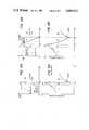
- FIG. 1is a cross-sectional view of an enhanced mobility, buried channel transistor structure in accordance with one embodiment of the invention
- FIG. 2Ais a chart illustrating the proportion of aluminum in the material versus the distance through the transistor structure for an enhanced mobility transistor of the prior art
- FIG. 2Bis a chart illustrating the proportion of aluminum in the material versus the distance through the transistor structure for an enhanced mobility, buried channel transistor structure having a tapered layer in accordance with one embodiment of the invention
- FIG. 3Ais a chart of electron energy versus distance throughout an enhanced mobility transistor of the prior art.
- FIG. 3Bis a chart of electron energy versus distance throughout an enhanced mobility, buried channel transistor structure in accordance with a preferred embodiment of the invention.
- FIG. 1there is depicted a crosssectional diagram of an enhanced mobility, buried channel transistor structure (EMBCT) in accordance with a preferred embodiment of the invention.
- EMBCTenhanced mobility, buried channel transistor structure
- a semi-insulating gallium arsenide substrate 11which acts as a quasi insulating support for the various epitaxial layers to be deposited thereupon.
- An undoped layer 12 of gallium arsenideis epitaxially deposited upon the semi-insulating gallium arsenide substrate 11.
- a layer 13 of Al x Ga 1-x Asis deposited upon the undoped layer 12 of gallium arsenide.
- the value of x for the layer 13 of Al x Ga 1-x Asvaries from a maximum quantity distant from the layer 12 of gallium arsenide to a minimum quantity (preferably zero) as the layers 13, 12 are in contact with one another.
- the value of xdesirably varies in a uniform manner, and, in a preferred mode, the thickness of the Al x Ga 1-x As layer 13 is in the order of 100 angstroms.
- Another layer 14 of undoped Al x Ga 1-x As(wherein the value of x is the maximum and constant) is deposited upon the tapered layer 13. Desirably, the various layers are epitaxially grown upon the substrate 11.
- a top layer 16 of n+ doped Al x Ga 1-x Asis deposited upon the constant undoped Al x Ga 1-x As layer 14.
- a source electrode 17is placed upon the doped layer 16.
- a drain electrode 18is placed upon the doped layer 16.
- a gate electrode 19is deposited upon the doped layer 16 between the source electrode 17 and the drain electrode 18.
- the electrodes 17, 19 and 18, respectively,can be deposited upon a doped layer 16 in accordance with techniques well known in the art through the use of Au/Ge and Ti/W contacts, respectively, for example.
- composition profile of the transistor structurehence has been modified to move the potential energy minimum away from layer 16. This has been achieved through the use of a graded or tapered Al x Ga 1-x As layer 13 where the aluminum concentration x is a function of the distance into the structure, as shown in FIGS. 1, 2B and 3B.
- the enhanced mobility, buried channel transistor structurehas its conducting channel located a distance (L 1 -L 0 ) away from the metallurgical interface of the layers 13, 14 at L 0 with the result that both coulomb interaction and interface scattering are reduced, thus resulting in a larger mobility enhancement for an enhanced mobility buried channel transistor in accordance with this invention, over conventional enhanced mobility transistor structures.
- xrepresents the proportional amount of aluminum in the wide bandgap material, and typically would be in the range of 0.2-0.4.
- a quasi 2-dimensional electron gasdoes not exist in the absence of an applied voltage for an enhancement mode device, but it does for a depletion mode device. Its existence depends upon the thickness of the heavily doped wide bandgap material and the doping level in that region.
- a quasi 2-dimensional electron gascan exist without the application of external biases although, in the case of enhancement mode devices, an external bias is required.
- a depletion mode devicewould have a 2-dimensional electron gas without a bias, and in an enhancement mode device, the quasi 2-dimensional electron gas does not exist unless an external bias is applied.
Landscapes
- Junction Field-Effect Transistors (AREA)
Abstract
Description
Claims (5)
Priority Applications (1)
| Application Number | Priority Date | Filing Date | Title |
|---|---|---|---|
| US06/660,175US4600932A (en) | 1984-10-12 | 1984-10-12 | Enhanced mobility buried channel transistor structure |
Applications Claiming Priority (1)
| Application Number | Priority Date | Filing Date | Title |
|---|---|---|---|
| US06/660,175US4600932A (en) | 1984-10-12 | 1984-10-12 | Enhanced mobility buried channel transistor structure |
Publications (1)
| Publication Number | Publication Date |
|---|---|
| US4600932Atrue US4600932A (en) | 1986-07-15 |
Family
ID=24648466
Family Applications (1)
| Application Number | Title | Priority Date | Filing Date |
|---|---|---|---|
| US06/660,175Expired - LifetimeUS4600932A (en) | 1984-10-12 | 1984-10-12 | Enhanced mobility buried channel transistor structure |
Country Status (1)
| Country | Link |
|---|---|
| US (1) | US4600932A (en) |
Cited By (10)
| Publication number | Priority date | Publication date | Assignee | Title |
|---|---|---|---|---|
| US4710478A (en)* | 1985-05-20 | 1987-12-01 | United States Of America As Represented By The Secretary Of The Navy | Method for making germanium/gallium arsenide high mobility complementary logic transistors |
| US4873558A (en)* | 1987-02-11 | 1989-10-10 | American Telephone And Telegraph Company, At&T Bell Laboratories | Group III-V compound field effect transistor with diffusion barrier |
| US4905056A (en)* | 1988-09-30 | 1990-02-27 | Berndt Dale F | Superlattice precision voltage reference |
| US4984036A (en)* | 1988-06-20 | 1991-01-08 | Mitsubishi Denki Kabushiki Kaishi | Field effect transistor with multiple grooves |
| EP0391380A3 (en)* | 1989-04-04 | 1991-05-15 | Siemens Aktiengesellschaft | Hemt structure |
| US5140386A (en)* | 1991-05-09 | 1992-08-18 | Raytheon Company | High electron mobility transistor |
| US5396103A (en)* | 1991-05-15 | 1995-03-07 | Minnesota Mining And Manufacturing Company | Graded composition ohmic contact for P-type II-VI semiconductors |
| US5986291A (en)* | 1993-10-12 | 1999-11-16 | La Corporation De L'ecole Polytechnique | Field effect devices |
| US6278143B1 (en)* | 1997-09-02 | 2001-08-21 | Sony Corporation | Semiconductor device with bipolar and J-FET transistors |
| US9735260B2 (en) | 2004-07-20 | 2017-08-15 | Toyota Jidosha Kabushiki Kaisha | III-V HEMT devices |
Citations (2)
| Publication number | Priority date | Publication date | Assignee | Title |
|---|---|---|---|---|
| EP0056904A2 (en)* | 1980-12-29 | 1982-08-04 | Fujitsu Limited | High electron mobility single heterojunction semiconductor devices and methods of production of such devices |
| EP0064370A2 (en)* | 1981-04-23 | 1982-11-10 | Fujitsu Limited | High electron mobility semiconductor device |
- 1984
- 1984-10-12USUS06/660,175patent/US4600932A/ennot_activeExpired - Lifetime
Patent Citations (2)
| Publication number | Priority date | Publication date | Assignee | Title |
|---|---|---|---|---|
| EP0056904A2 (en)* | 1980-12-29 | 1982-08-04 | Fujitsu Limited | High electron mobility single heterojunction semiconductor devices and methods of production of such devices |
| EP0064370A2 (en)* | 1981-04-23 | 1982-11-10 | Fujitsu Limited | High electron mobility semiconductor device |
Non-Patent Citations (2)
| Title |
|---|
| Lee et al., "High Temperature Annealing of Modulation Doped GaAs/AlGaAs Heterostructures for FET Applications", Proceedings IEEE/Cornell Conference on High-Speed Semiconductor Devices & Circuits, Aug. 1983, pp. 204-208. |
| Lee et al., High Temperature Annealing of Modulation Doped GaAs/AlGaAs Heterostructures for FET Applications , Proceedings IEEE/Cornell Conference on High Speed Semiconductor Devices & Circuits, Aug. 1983, pp. 204 208.* |
Cited By (12)
| Publication number | Priority date | Publication date | Assignee | Title |
|---|---|---|---|---|
| US4710478A (en)* | 1985-05-20 | 1987-12-01 | United States Of America As Represented By The Secretary Of The Navy | Method for making germanium/gallium arsenide high mobility complementary logic transistors |
| US4873558A (en)* | 1987-02-11 | 1989-10-10 | American Telephone And Telegraph Company, At&T Bell Laboratories | Group III-V compound field effect transistor with diffusion barrier |
| US4984036A (en)* | 1988-06-20 | 1991-01-08 | Mitsubishi Denki Kabushiki Kaishi | Field effect transistor with multiple grooves |
| US5362677A (en)* | 1988-06-20 | 1994-11-08 | Mitsubishi Denki Kabushiki Kaisha | Method for producing a field effect transistor with a gate recess structure |
| US4905056A (en)* | 1988-09-30 | 1990-02-27 | Berndt Dale F | Superlattice precision voltage reference |
| EP0391380A3 (en)* | 1989-04-04 | 1991-05-15 | Siemens Aktiengesellschaft | Hemt structure |
| US5393990A (en)* | 1989-04-04 | 1995-02-28 | Siemens Corporate Research, Inc. | HEMT structure |
| US5140386A (en)* | 1991-05-09 | 1992-08-18 | Raytheon Company | High electron mobility transistor |
| US5396103A (en)* | 1991-05-15 | 1995-03-07 | Minnesota Mining And Manufacturing Company | Graded composition ohmic contact for P-type II-VI semiconductors |
| US5986291A (en)* | 1993-10-12 | 1999-11-16 | La Corporation De L'ecole Polytechnique | Field effect devices |
| US6278143B1 (en)* | 1997-09-02 | 2001-08-21 | Sony Corporation | Semiconductor device with bipolar and J-FET transistors |
| US9735260B2 (en) | 2004-07-20 | 2017-08-15 | Toyota Jidosha Kabushiki Kaisha | III-V HEMT devices |
Similar Documents
| Publication | Publication Date | Title |
|---|---|---|
| US5705827A (en) | Tunnel transistor and method of manufacturing same | |
| EP0033037B1 (en) | Heterojunction semiconductor devices | |
| US4827320A (en) | Semiconductor device with strained InGaAs layer | |
| US4987462A (en) | Power MISFET | |
| US5111255A (en) | Buried channel heterojunction field effect transistor | |
| US4704622A (en) | Negative transconductance device | |
| JPS6342864B2 (en) | ||
| US4740822A (en) | Field effect device maintaining a high speed operation in a high voltage operation | |
| US4772925A (en) | High speed switching field effect transistor | |
| JP3376078B2 (en) | High electron mobility transistor | |
| JP2914049B2 (en) | Compound semiconductor substrate having heterojunction and field effect transistor using the same | |
| US4600932A (en) | Enhanced mobility buried channel transistor structure | |
| EP0566591B1 (en) | Semiconductor device | |
| Mimura | The present status of modulation-doped and insulated-gate field-effect transistors in III–V semiconductors | |
| US4903091A (en) | Heterojunction transistor having bipolar characteristics | |
| US5751029A (en) | Field-effect semiconductor device having heterojunction | |
| Fritzsche | Heterostructures in MODFETs | |
| EP0136108A1 (en) | Heterojunction semiconductor device | |
| JPH08255898A (en) | Semiconductor device | |
| EP1083608B1 (en) | Field-effect semiconductor device | |
| Kusters et al. | Sub-half-micrometer pseudomorphic InP/In/sub x/Ga/sub 1-x/As/InP HEMT's (0.74/spl les/x/spl les/0.81) with very high f T values | |
| Prost et al. | High speed, high gain InP-based heterostructure FETs with high breakdown voltage and low leakage | |
| JP2659181B2 (en) | Semiconductor device | |
| JPH04277680A (en) | Tunnel transistor and manufacture of the same | |
| JP2701632B2 (en) | Enhancement type field effect transistor |
Legal Events
| Date | Code | Title | Description |
|---|---|---|---|
| AS | Assignment | Owner name:GTE LABORATORIES INCORPORATED A CORP OF DE Free format text:ASSIGNMENT OF ASSIGNORS INTEREST.;ASSIGNOR:NORRIS, PETER E.;REEL/FRAME:004325/0457 Effective date:19841012 | |
| STCF | Information on status: patent grant | Free format text:PATENTED CASE | |
| FEPP | Fee payment procedure | Free format text:PAYOR NUMBER ASSIGNED (ORIGINAL EVENT CODE: ASPN); ENTITY STATUS OF PATENT OWNER: LARGE ENTITY | |
| FEPP | Fee payment procedure | Free format text:PAYER NUMBER DE-ASSIGNED (ORIGINAL EVENT CODE: RMPN); ENTITY STATUS OF PATENT OWNER: LARGE ENTITY Free format text:PAYOR NUMBER ASSIGNED (ORIGINAL EVENT CODE: ASPN); ENTITY STATUS OF PATENT OWNER: LARGE ENTITY | |
| FPAY | Fee payment | Year of fee payment:4 | |
| FPAY | Fee payment | Year of fee payment:8 | |
| REMI | Maintenance fee reminder mailed | ||
| FPAY | Fee payment | Year of fee payment:12 | |
| SULP | Surcharge for late payment | ||
| FEPP | Fee payment procedure | Free format text:PAYER NUMBER DE-ASSIGNED (ORIGINAL EVENT CODE: RMPN); ENTITY STATUS OF PATENT OWNER: LARGE ENTITY Free format text:PAYOR NUMBER ASSIGNED (ORIGINAL EVENT CODE: ASPN); ENTITY STATUS OF PATENT OWNER: LARGE ENTITY |