US4600918A - Equipment for reproduction of alphanumerical data - Google Patents
Equipment for reproduction of alphanumerical dataDownload PDFInfo
- Publication number
- US4600918A US4600918AUS06/393,127US39312782AUS4600918AUS 4600918 AUS4600918 AUS 4600918AUS 39312782 AUS39312782 AUS 39312782AUS 4600918 AUS4600918 AUS 4600918A
- Authority
- US
- United States
- Prior art keywords
- block
- data
- ram
- characters
- character
- Prior art date
- Legal status (The legal status is an assumption and is not a legal conclusion. Google has not performed a legal analysis and makes no representation as to the accuracy of the status listed.)
- Expired - Lifetime
Links
Images


Classifications
- G—PHYSICS
- G09—EDUCATION; CRYPTOGRAPHY; DISPLAY; ADVERTISING; SEALS
- G09G—ARRANGEMENTS OR CIRCUITS FOR CONTROL OF INDICATING DEVICES USING STATIC MEANS TO PRESENT VARIABLE INFORMATION
- G09G5/00—Control arrangements or circuits for visual indicators common to cathode-ray tube indicators and other visual indicators
- G09G5/22—Control arrangements or circuits for visual indicators common to cathode-ray tube indicators and other visual indicators characterised by the display of characters or indicia using display control signals derived from coded signals representing the characters or indicia, e.g. with a character-code memory
- G09G5/222—Control of the character-code memory
- H—ELECTRICITY
- H03—ELECTRONIC CIRCUITRY
- H03J—TUNING RESONANT CIRCUITS; SELECTING RESONANT CIRCUITS
- H03J1/00—Details of adjusting, driving, indicating, or mechanical control arrangements for resonant circuits in general
- H03J1/0008—Details of adjusting, driving, indicating, or mechanical control arrangements for resonant circuits in general using a central processing unit, e.g. a microprocessor
- H03J1/0016—Indicating arrangements
- H—ELECTRICITY
- H03—ELECTRONIC CIRCUITRY
- H03J—TUNING RESONANT CIRCUITS; SELECTING RESONANT CIRCUITS
- H03J1/00—Details of adjusting, driving, indicating, or mechanical control arrangements for resonant circuits in general
- H03J1/0008—Details of adjusting, driving, indicating, or mechanical control arrangements for resonant circuits in general using a central processing unit, e.g. a microprocessor
- H03J1/0041—Details of adjusting, driving, indicating, or mechanical control arrangements for resonant circuits in general using a central processing unit, e.g. a microprocessor for frequency synthesis with counters or frequency dividers
- H03J1/005—Details of adjusting, driving, indicating, or mechanical control arrangements for resonant circuits in general using a central processing unit, e.g. a microprocessor for frequency synthesis with counters or frequency dividers in a loop
- H—ELECTRICITY
- H03—ELECTRONIC CIRCUITRY
- H03J—TUNING RESONANT CIRCUITS; SELECTING RESONANT CIRCUITS
- H03J5/00—Discontinuous tuning; Selecting predetermined frequencies; Selecting frequency bands with or without continuous tuning in one or more of the bands, e.g. push-button tuning, turret tuner
- H03J5/02—Discontinuous tuning; Selecting predetermined frequencies; Selecting frequency bands with or without continuous tuning in one or more of the bands, e.g. push-button tuning, turret tuner with variable tuning element having a number of predetermined settings and adjustable to a desired one of these settings
- H03J5/0245—Discontinuous tuning using an electrical variable impedance element, e.g. a voltage variable reactive diode, in which no corresponding analogue value either exists or is preset, i.e. the tuning information is only available in a digital form
- H03J5/0272—Discontinuous tuning using an electrical variable impedance element, e.g. a voltage variable reactive diode, in which no corresponding analogue value either exists or is preset, i.e. the tuning information is only available in a digital form the digital values being used to preset a counter or a frequency divider in a phase locked loop, e.g. frequency synthesizer
- H03J5/0281—Discontinuous tuning using an electrical variable impedance element, e.g. a voltage variable reactive diode, in which no corresponding analogue value either exists or is preset, i.e. the tuning information is only available in a digital form the digital values being used to preset a counter or a frequency divider in a phase locked loop, e.g. frequency synthesizer the digital values being held in an auxiliary non erasable memory
Definitions
- the present inventionrelates to an equipment for reproduction of alphanumerical data, which comprises an operating unit having an alphanumerical keyboard adapted to generate at least as many coded control signals as the characters which can be generated for reproduction, a control unit for the detection of the control signals generated by the operating unit, and circuit means for the generation, through reproducer means, of alphanumerical data formed by the characters selected by means of the operating unit.
- the equipmentin its various configurations, may be a television set provided with an alphanumerical display device adapted to display alphanumerical data on the television screen; it may be a generic apparatus, in particular a television set, provided with color picture display means for displaying the alphanumerical data; it may be a radioelectric signal receiver, for example a television set or a radio set, provided with an alphanumerical character display device; it may be an apparatus comprising means for the reproduction of alphanumerical data on a display screen (television set, peripheral unit in a computer system, etc.) or reproducer printing device (typewriter, printing machine in a computer system) or vocal reproducer devices.
- a television setprovided with an alphanumerical display device adapted to display alphanumerical data on the television screen
- itmay be a generic apparatus, in particular a television set, provided with color picture display means for displaying the alphanumerical data
- itmay be a radioelectric signal receiver, for example a television set or a radio set,
- the known prior art apparatusesare designed to perform various functions (for example, for a television set, direct channel selection, the memorization of a large number of programs, time display, timed turn-on or program switching, etc.) which can be performed easily with the aid of a suitably programmed microprocessor.
- the television setsare preferably fitted with display devices for supplying data relative to the foregoing functions.
- these display devicesare usually only designed to provide a numerical indication of the time, channel and/or program, and the keyboards by means of which the foregoing functions are controlled possess a limited number of keys which cannot allow a large number of operations on the set.
- the microprocessoris not used to a sufficient extent as regards its data processing capacity, because of the insufficiency of the display means connected to it and the control device supplying it with the data to be processed.
- the object of the present inventionis to provide sets of the types mentioned hereinabove which in the performance of their various specific functions and in their control system are more sophisticated than the prior art sets, with no substantial increase in the complexity and cost of the circuits.
- a television receiverfitted with a television screen and circuit means for generating a picture to be displayed, connected to the television screen, for displaying, following a control from the user, in substitution of the received video picture, another complete picture composed of alphanumerical data formed by characters which may comprise all the letters in the alphabet, the numbers from 0 to 9 and graphic symbols.
- the inventioncomprises a control unit, connected to the circuit means, to first read-write (RAM) memory means and to an operating unit for receiving data from the user, characterized by the fact that the operating unit comprises an alphanumerical keyboard for generating at least as many coded control signals as the characters which may be generated by the circuits and displayed on the television screen, these operating signals being decoded by the control unit, sent to the circuits in order to allow displaying the corresponding characters on the screen and stored by the control unit in the first read-write memory means for repeat display on the screen at any time in response to a given display control operated by the user.
- RAMfirst read-write
- the present inventionalso provides a set fitted with color picture display means, comprising circuit means for generating color pictures, for displaying, following a operating control from the the user, data composed of at least one of the color pictures, composed of alphanumerical characters including at least the numbers from 0 to 9.
- the inventionfurther comprises a control unit, connected both to the circuit means and to an operating unit for receiving data from the user, characterized by the fact that the operating unit comprises a keyboard for generating coded control signals which are sent to and decoded by the control unit, and that the control unit, when it receives the coded control signals, determines the day of the week corresponding to a given date set by the coded control signals entered by the user on the operating unit and supplies the display means with data relative to the alphanumerical characters to be displayed, so as to display the picture on a screen in at least two colors showing at least the calendar month containing the date determined by the coded control signal entered by the user.
- the operating unitcomprises a keyboard for generating coded control signals which are sent to and decoded by the control unit, and that the control unit, when it receives the coded control signals, determines the day of the week corresponding to a given date set by the coded control signals entered by the user on the operating unit and supplies the display means with data relative to the alphanumerical characters to be
- the present inventionalso provides a radioelectric signal receiver fitted with at least an alphanumerical character display device, comprising a control unit connected to circuit means for controlling the display device, to radioelectric signal tuning means, to first electronic memorizing means for memorizing at least data relative to the tuning of the radioelectric signals, and to an operating unit for receiving data from the user, characterized by the fact that, in response to a first coded control signal corresponding to a message composed of alphanumerical characters and representative of the station which transmits the radioelectric signal from the operating unit, the control unit extracts from the first memorizing means the data relative to the tuning of the radioelectric signal to be sent to the tuning means, and supplies the circuit means with codes adapted to obtain the reproduction of the message on the display device.
- the present inventionprovides a receiver comprising reproducer means for reproducing on a display screen, or printing reproducer means or vocal reproducer means, alphanumerical data formed by characters which may comprise all the letters in the alphabet, the numbers from 0 to 9 and graphic symbols, characterized by the fact that it comprises a telecontrol type operating unit comprising an alphanumerical keyboard adapted to generate at least as many coded control signals as the characters which can be generated for reproduction by the reproducer means, a control unit for the detection of the control signals generated by the operating unit, and circuit means which through the reproducer means generate the said alphanumerical data formed by the selected characters.
- a telecontrol type operating unitcomprising an alphanumerical keyboard adapted to generate at least as many coded control signals as the characters which can be generated for reproduction by the reproducer means, a control unit for the detection of the control signals generated by the operating unit, and circuit means which through the reproducer means generate the said alphanumerical data formed by the selected characters.
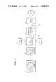
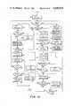
- FIG. 1shows a block diagram of a television set improved according to the present invention
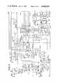
- FIG. 2shows a wiring diagram of some of the circuits shown diagrammatically in FIG. 1;
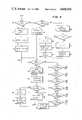
- FIGS. 3-14show block diagrams of the elementary functions performed by the circuits inserted inside the television set according to the invention.
- FIG. 15shows a block diagram of a different embodiment of a set according to the present invention.
- reference numeral 1indicates a remote-control transmitter comprising an alphanumerical keyboard composed conveniently of 64 keys and known infrared ray transmission and coding circuits (Motorola MC14497 integrated circuit).
- Number 2is an infrared ray receiver circuit comprising an amplifier (Motorola TBA 2110 integrated circuit) whose output is connected to control unit 3 comprising a Fairchild 3872 microcomputer.
- the control unitis also connected to:
- RAM 7a random access CMOS memory (RAM) 7 consisting of (512) 8-bit cells and made using two RCA MW5113 512*4 RAM memories;
- a PLL frequency synthesis circuit 8 for direct channel tuningconsisting of a Motorola UAA 2000 integrated circuit
- a character generating circuit 4for displaying 64 types of alphanumerical characters on the screen with a 5 ⁇ 7 dot matrix arranged in 8 lines of 32 characters;
- the character generating circuithas three outputs (R', G', B') connected to inputs R, G and B respectively on final video circuit 5.
- the latteralso receives at inputs R, G and B the three red, green and blue color signals sent out from the brightness and color circuits on the set and has three outputs connected to the cathodes of color kinescope 6.
- Remote-control transmitter 1consists of:
- the first set of functionsincludes the letters of the alphabet and the second the arabic numbers or punctuation marks.
- TACthree keys, TAC, CAL and DSP, for selecting the required function: scratch pad, calendar or return to normal receiver function control.
- the MC 14497 integrated circuittransmits a special signal in two-phase FSK code, i.e. a series signal consisting of two packs of two given frequencies for each bit in the number of the key that has been pressed.
- Receiver-amplifier circuit 2then amplifies and demodulates the received signal into a timed sequence of ones and zeroes. Whenever a key is released, integrated circuit MC 14497 automatically transmits an end-of-transmission code corresponding to control 63.
- Control unit 3decodes the timed sequence into the corresponding code of the key that has been pressed. When one of the TAC, CAL or DSP function keys is pressed, the control unit switches to the corresponding operating mode as described later on with reference to FIG. 3.
- control unitcalls up data (scratch pad message) from memory circuits 7 and sends it to character generating circuit 4 for display on the screen, after which it prepares to receive further instructions from the transmitter which it stores in RAM 7 for forming a new message.
- control unitsends character generator 4 the following message:
- control unitcalculates the date of the first day in the month requested, draws up a seven-column table of four or five lines showing all the days in the month and sends it to character generator 4.
- the calendar displayed on the screenmay look like this:
- the month and year (December 1980)are displayed in red, the days of the week, (MO, TU, WE, TH, FR, SA) in magenta, the numbers usually in white and "SU” and public holiday numbers (7, 14, 21, 28, 25) in red.
- control unitprepares for ordinary television functions (channel/program selection, level adjustments, memorization, etc.).
- control unitcalls up tuning data relative to the selected program number from RAM 7, calculates the dividing number, which it sends in code to PLL circuit 8 for tuning into the required channel, and sends the data to be displayed (selected program/channel number, etc.) to character generator 4. For certain programs, it also supplies terminal "AV" with a time constant switch signal.
- control unit microcomputercontains a block of registers (SPAD), consisting of (64) 8-bit registers, and a RAM memory area (BUFFER), consisting of 64 RAM memory cells ranging between the "FCO” and "FFF" addresses in hexadecimal notation.
- SSDblock of registers
- BAFFERRAM memory area
- DATAindicates six input terminals representing the ASCII code of the 64 symbols which may be displayed.
- ADDindicates three terminals representing the selected print line number (0-7 on an 8-line display).
- DTindicates a terminal for enabling data transmission to the character generating circuit.
- DCindicates a clock terminal for moving the character forward on a given line.
- FH and FVindicate two sync terminals, for the horizontal and the vertical frequency, depending on the scanning of the set.
- R', G', B'indicate three output terminals for supplying red, green and blue display picture data which is amplified and then sent to the kinescope.
- the character generating 4 circuitessentially consists of a Fairchild 3258 integrated circuit for generating a 64-character display matrix, a Fairchild 3539 256 ⁇ 8 RAM memory, a clock generator consisting of Fairchild IO10 (74LS02) and IC9 (74LS163) integrated circuits and character and line counters, for supplying addresses to the memory circuit, consisting of Fairchild IO2 (4024) and IC4 (4029) integrated circuits with the auxiliary circuits and connections shown in FIG. 2.
- the line numberFor printing on a given line, the line number must first be supplied to the "ADD" terminals so as to set the line counter to the required value. A signal is then sent to the "DT" terminal for setting the memory to print mode, followed by the display character and clock pulse which are sent respectively to the "DATA" and "COLOUR” and “DC” terminals.
- the entered datais thus stored in successive memory cells in the area set aside for the selected line.
- the character generating circuit 4has another two input terminals ("CS" and "OFF")--one for print enabling the character generator RAM memory and the other for disabling any printing on the screen--both connected to appropriate outputs on the microcomputer control unit.
- FIG. 3shows reading and decoding of the controls received from amplifier 2 in FIG. 1 and function selection.
- Number 1 in FIG. 3indicates an initialization block which, when activated by an "ON" signal, assigns specific initial values to the registers and TIMER and arranged for the "receiver control" function.
- the initialization blockactivates the next block (2) which reads the input signal from amplifier 2 in FIG. 1 and, in turn, activates block 3, which checks whether the signal is 0.
- the "YES” output of block 3activates block 4, which checks whether the "DAT" register contains a preset "CROT” value.
- the "NO” output of block 4supplies the signal for activating block 2 while the "YES” output activates block 5, which, after a set pause, supplies a "CALEN” signal for activating the blocks in FIG. 9.
- the "NO” output of block 3activates the next block (6), which checks whether the input signal contains a START BIT.
- the "NO” outputsupplies a signal for activating block 2 while the "YES” output activates in turn:
- the "NO” output of block 9supplies a signal for activating block 2 while the "YES” output activates block 10, which checks whether the "DAT" register contains a set of "FUNCTION” (>50) values.
- the "YES” outputactivates block 11, which arranges for the new function and stores the contents of the "DAT” register in the "FUNCTION” register, while the "NO" output of block 10 and the output of block 11 activate in turn:
- the "YES” output of block 12supplies a "CALE” signal for activating the blocks described later in FIG. 8.
- the "YES” output of block 13supplies a "TACC” (scratch pad) signal for activating the blocks described later in FIG. 4, while the "NO” output supplies a "STAR" signal for activating the television function control blocks described later in FIG. 11.
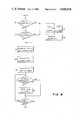
- FIG. 4shows block diagrams of the basic "TACC” logic functions performed by the control unit.
- the "TACC" signal received from block 13 in FIG. 3activates block 20, which checks whether the "DAT" register contains a prearranged "TAC” value (i.e. whether the scratch pad function key has just been pressed on keyboard 1 in FIG. 1).
- block 23which supplies the character generating circuit with first line data and positions the "pointer" character in the first top left-hand position on the screen.
- Block 23then supplies an enabling (LOOP) control to block 2 in FIG. 3.
- the "NO” output of block 20activates block 24, which checks whether the "DAT” register contains a prearranged “RAND” value, while the "YES” output of block 24 activates in turn:
- the "YES" output of block 27then activates block 31, which clears the F signal, and block 32, which sends the ROM code sequence to the character generating circuit.
- Blocks 30 and 32supply the enabling signal to block 2 in FIG. 3.
- block 24activates block 25, which, depending on the line number ("ADD" register) and pointer position ("CRT” register), sets the pointer to a particular cell in RAM memory 7 in FIG. 1.
- Block 25activates block 33, which checks whether the content of the "DAT" register belongs to the group of control function values (>32).
- the "NO" output(data for display) activates in turn:
- the "YES" output of block 36activates in turn block 37, which sends all the line data to the character generating circuit, and block 38, which alters the content of the "ADD" (line pointer) register.
- block 39which sends the new line data to the character generating circuit and an enabling signal to block 2 in FIG. 3.
- the "YES" outputs of blocks 40-45supply signals RET, SHI, PF, PB, PD and CL respectively for enabling the next blocks in FIGS. 5-7.
- Block 46supplies the activating signal to block 39.
- FIG. 5shows the reading of a line in RAM memory 7 of FIG. 1 and transmission to the character generating circuit, i.e. operation of FIG. 4 blocks, such as 22, 23, 37 and 39, in greater detail.
- Number 50 in FIG. 5indicates a block which, depending on the present line number in the "ADD" register, initializes a pointer register at a given cell in RAM memory 7 in FIG. 1.
- the block 50activates in turn:
- block 53which checks whether the position of the character that has just been read tallies with the position of the pointer.
- the "NO" output of block 56supplies an enabling signal to block 52, while the "YES” output enables block 57, which waits for a vertical-frequency sync pulse, after which it supplies an enabling signal to block 58, which transfers the line data stored in the BUFFER to the character generating circuit.
- FIGS. 6 and 7show block diagrams of the elementary functions performed by the microcomputer control unit for controlling composition of the printed text.
- FIG. 6shows the page clearing functions and pointer shift with or without clearing and
- FIG. 7the shift function and pointer shift to the right or left.
- the "NO” output of block 62supplies an enabling signal to block 60, while the "YES” output supplies an enabling signal to block 63, which checks whether the "DAT" register contains a preset "CLEAR” value (clear key); the "YES” output activates block 64, which modifies the pointer registers to indicate the start of the next line and activates block 67, which checks whether the end of the last line has been reached; the "YES” output supplies signal TC1 to block 21 in FIG. 4, while the "NO” output supplies an enabling signal to block 60.
- the "NO" outputactivates in turn:
- block 66which points to the start of the next line and supplies an enabling signal to block 2 in FIG. 3 (await new data).
- the "YES” output of block 72activates block 73, which sets the pointers at the start of the next line, and block 74, which transmits a line of characters to the character generating circuit.
- the "NO" output of block 72 and block 74supply an enabling signal to block 2 in FIG. 3.
- the "SHI” output from block 41 in FIG. 4activates block 75, which modifies the "SHIFT” function bit (first or second function group selection on the keyboard) and supplies an enabling signal to block 74.
- the "PB” signal from block 43 in FIG. 4activates block 76, which increases the content of counter “CRT” (pointer one place back shift), and block 77, which checks whether the pointer was positioned at the start of a line.
- the "NO” outputactivates block 74, while the “YES” output activates, in turn, block 78, which transmits a line of characters to the character generating circuit, and block 79, which sets the pointers at the end of the previous line.
- the output of block 79supplies an enabling signal to block 74.
- the pointer characterWhen operated, the pointer character changes to inform the user, by means of a visual aid, which group of characters has been selected ("-" for letters, " " for numbers).
- the pointeralso changes color whenever the "COL" key is pressed (white, red, yellow, magenta) to remind the user which color has been selected for display.
- Each character enteredis automatically stored in the memory.
- the content of the present lineis transmitted to the character generator. Transmitting a whole line each time is the best compromise between transmission speed and the number of connections required and also guarantees constant character alignment.
- the scratch pad functionalso includes two fixed messages, generated by the control unit regardless of the message compiled by the user.
- the first fixed messageconcerns the more common receiver operating instructions and consists of a full-page message stored in the ROM, as opposed to the RAM, on the microcomputer during masking.
- the secondcorresponds to the entire group of display characters produced by the microcomputer unit (all 256 possible 8-bit data values displayed by the character generating circuit in four groups of 64 characters in four colors over eight lines) which serves both as a memo for the user and for making a fast check of correct circuit operating during stop testing.
- a special meaninghas been assigned to the last line in the scratch pad, which may be used for memorizing special dates, such as birthdays, anniversaries, appointments, etc.
- Tables 1 and 2show, in hexadecimal form, the internal connections of each cell in the ROM memory on microcomputer integrated circuit 3872, which constitutes the cell control unit.
- Table 1shows the blocks in FIG. 3 for reading and decoding the controls received from the remote control and selecting the functions to be performed.
- Table 2shows the blocks in FIGS. 4-7 for performing the "SCRATCH PAD" function, i.e. displaying a message stored beforehand in the RAM memory and compiling and storing a new message.
- FIG. 8shows data entry (month and year) for the calender call-up function.
- the "CALE” signal from block 12 in FIG. 3activates block 80, which checks whether the "TAS" register contains a preset "CAL” value (i.e. whether the calender function button has just been operated).
- the "NO” outputactivates, in turn, block 81, which stores the operated key code in a cell in the RAM memory buffer inside the microprocessor, and block 82, which alters the content of a digit count register.
- the "YES” output of block 80activates, in turn, block 83, which assigns an initial value to said digit count register, and block 84, which stores the "??/????" character codes in the memory buffer.
- Blocks 82 and 84both activate:
- block 87which checks whether the data entered is the last figure in the number of the year.
- the "YES” output of block 87supplies a "CALEN” signal to the blocks described later in connection with FIG. 9.
- the "NO” outputsupplies a signal for activating block 2 in FIG. 3 (await new data).
- FIG. 9shows how Easter and the calender of a given month are calculated for the set year.
- the "CALEN" signal from block 87 in FIG. 8activates block 90, which checks whether the set month number (1-12) is acceptable: the "YES” output activates block 91, which checks whether the century number falls within a given range (16-24), while the "NO" output of blocks 90 and 91 activate in turn:
- block 92which assigns limit numbers 1 or 12 to the number of the month and 1600 or 2499 to the number of the year;
- block 95which, starting from the year and century number, calculates the date of Easter Sunday using the known Gauss formula and stores it in the "TE1" register;
- the "YES" output of block 97(indicating that the requested month is among the dates to be remembered) activates block 98, which stores the number of the day to be remembered in a "SPAD" register.
- Block 98 and the "NO" output of block 97activate block 99, which checks whether the data to be remembered is the last one in the RAM memory.
- FIG. 10shows block diagrams of elementary logic functions performed by the control unit for displaying a calender page.
- the "DSP" signal from block 99 in FIG. 9activates block 100, which sets the color yellow and activates block 101, which checks whether it is the first line.
- the "YES" output of block 101(line containing the name of the month and the year) activates in turn:
- the output of block 106supplies a signal for activating block 101 the "NO" output of which activates block 107, which checks whether it is the second line.
- the "YES” output of block 107(line containing abbreviations of the days of the week: MO, TU, WE, TH, FR, SA, SU) activates block 108, which sets the color magenta, and block 109, which checks whether it is the last column.
- the "YES” output(Sundays) activates block 110, which sets the color red, while the "NO" output and the output of block 110 activate, in turn, block 111, which sends two data from the ROM and two blanks to the character generating circuit, and block 112, which checks whether it is the end of a line.
- the "NO" output of block 128(incomplete calender page) supplies a signal for activating block 101, while the "YES” output (complete page; increment month and year for rotating calendar) activates block 129, which checks whether the number of the month is 12.
- the "NO” outputactivates block 131, which increments the number of the month, while the "YES” output activates block 130, which assigns a 1 to the number of the month and increments the number of the year.
- the outputs of blocks 130 and 131supply a signal for activating block 2 in FIG. 3 (end of calender, await new instructions; if the "CROT" key has been pressed, after a certain length of time, the "CALEN” signal is generated again and the next month's calender is displayed on the screen).
- the "NO" output of block 120activates block 121, which sets the color red.
- Blocks 119 and 121 and the "NO" output of block 120activate, in turn, block 122, which sends "DATA" relative to the day of the month and two blanks of the character generating circuit, and block 123, which checks whether the date corresponds with the length of the month.
- block 123activates block 124, which assigns the "DATA" a blank code (to fill in with blanks after the last day of the month).
- Block 124 and the "NO" output of block 123activate block 125, which checks whether it is the end of a line.
- the "NO” outputactivates block 117, while the "YES” output activates block 126.
- Table 3shows the blocks in FIG. 3 relative to the calendar data entry function.
- Table 4shows the blocks in FIG. 9 for calculating Easter Sunday and the first day of the month requested, as well as examining the dates to be remembered.
- Table 5shows the blocks in FIG. 5 for transmitting data to the character generating circuit for displaying a calendar page in different colors.
- FIG. 11shows operation mode selection (favorite program selection, etc.), "SHIFT” and memory page switch functions, return to normal television operation and memorization of program-associated station labels.
- the "STAR" signal in FIG. 11 from block 13 in FIG. 3activates block 130, which checks whether the operated key corresponds to a preset "DSP" code (return to normal operation of the set).
- the "YES” output of block 130activates block 150, which checks whether, instead of the key number, the buffer contains the "?” code.
- the "NO" output of block 150activates, in turn, block 152, which checks whether, instead of the label, the buffer contains a "?", and block 153, which checks whether, instead of the channel number, the buffer contains a "?”.
- the "YES" output of block 150activates block 151, which recovers the key number from one of the internal SPAD registers.
- the "YES” output of block 152activates block 154, which clears the label in the buffer.
- the "YES” output of block 153activates block 155, which recovers the channel number from the SPAD.
- the outputs of blocks 151 and 154 and the "NO" output of block 153activate block 156, which checks whether the key number is between 0 and 9.
- the "YES” outputsupplies an "INDIR” signal to the blocks in FIG. 13, while the "NO” output and the output of block 155 supply a "DIRET” signal to the next receiver blocks for selecting a station in the usual way on the basis of a given transmission standard channel number.
- the "NO" output of block 130activates block 131, which checks whether the operated key corresponds to a given "SHIFT” code.
- the "YES” output of block 131activates block 133, which checks whether the "SHIFT” function bit is 1: the "YES” output activates block 134, which zeroes the bit, while the “NO” output activates block 135, which sets the bit to 1.
- Blocks 134 and 135supply a signal for activating block 163, which transmits the words "CHANNEL” and "KEY” to the character generating circuit together with the memory page, channel and program numbers and a label if there is one.
- a typical display in this caseis:
- the "NO” output of block 131activates block 132, which checks whether the operated key corresponds to a given "PAG” code.
- the "YES” outputactivates, in turn, block 136, which increments the page number within a 1-3 range, block 137, which stores the page number in the buffer, and display block 163.
- the "NO” outputactivates block 138, which checks whether the operated key corresponds to a given "PRG” code.
- the "YES” output of block 138activates block 139, which checks whether the operated key corresponds to a code from 11-13; the "YES” output supplies a "FINET” signal to the next blocks on the set which perform a tuning correction, while the "NO” output activates, in turn, block 140, which saves the operated key in a "MOO” mode register, and block 141, which checks whether the "MOO" register contains a preset 19 code.
- the “YES” output of block 141supplies a "MEMOR” signal to the blocks in FIG. 12, while the “NO” output supplies an enable signal to block 142, which checks whether the "MOO" register contains a preset code 48.
- the "YES” outputsupplies a "PRG” signal to the blocks in FIG. 14, while the “NO” output supplies a signal to the next blocks in FIG. 13.
- the "NO" output of block 138activates, in turn, block 143, which stores the operated key in register "TE1", and block 144, which checks whether the "MOO" register contains a preset code 49 (label memorization).
- the "YES” output of block 146activates block 147, which saves the operated number in the buffer and supplies an enabling signal to block 141.
- the "YES” outputs of blocks 145, 148 and 149supply an enabling signal to block 139.
- the "NO” output of block 149supplies a "RICER” signal to the next blocks on the set which automatically scan the memorized programs and receivable channels.
- Block 162supplies a signal for activating display block 163 and for generating the "LOOP" signal for awaiting new instructions.
- FIG. 12shows map display of the channels on a memory page and memorization of channel data for assigning it to a given key.
- the "MEMOR" signal from block 141 in FIG. 11activates block 170, which checks whether the operated key corresponds to a preset "MEM” value (memorization button).
- block 171which assigns an initial value of 9 to the count register and points to an initial cell in RAM 7 of FIG. 1;
- block 173activates block 174, which reads the tuning, color, volume and brightness data from the RAM memory and stores it in four "SPAD" registers.
- Block 174 and the "YES" output of block 173activate, in turn, block 175, which reads the channel number from the RAM memory and stores it in the "RD" register, and block 176, which checks whether the read data is valid.
- the "NO” output of block 176activates block 177, which assigns a fictitious "FF" number to the channel, while the output of block 177 and the "YES” output of block 176 activate, in turn:
- the "NO” output of block 180activates block 181, which assigns an "FF" number to the channel, while the "YES” output activates block 182, which stores the label data in the buffer.
- Blocks 181 and 182activate, in turn, block 183, which stores the channel number in the "SPAD", and block 184, which checks whether the key count register contains a zero.
- the "NO" output of block 184supplies a signal for activating block 172, while the “YES” output supplies a signal for activating block 185, which sends the numbers of 10 channels on a given memory page to the character generating circuit for displaying the map.
- a typical channel map displayis:
- Blocks 172 to 177form a single block, which we shall call “READ”, for reading all the program data from the RAM memory.
- Blocks 178-182also form a single block, which we shall call “ETI”, for reading the label data from the RAM memory. Both “READ” and “ETI” blocks will be used again later.
- the "NO" output of block 170activates block 186, which checks whether the operated key corresponds to a number from 0 to 9.
- the "NO” output(second time the "MEM” key has been operated) activates, in turn, block 187, which clears the previous label in the buffer, and block 188, which checks whether the channel number is valid.
- Block 188activates block 190, which stores a "?” in the buffer to show that the receiver is waiting for the key number to be stored, while the "NO" output activates block 189, which supplies an error signal (short sound).
- Blocks 189 and 190supply an enabling signal to block 2 in FIG. 3 (await further instructions).
- block 194which stores tuning, color, volume, brightness and channel data in five consecutive RAM cells;
- Block 198supplies an enabling signal to block 163 in FIG. 11 (await three label characters) which are then stored when blocks 157-162 in FIG. 11 (PET) are activated.
- a typical display during label memorizationis:
- each labelconsists of three characters which may be letters of the alphabet, numbers or blanks.
- a special significancehas been assigned, however, to labels whose first two letters are "VC", i.e. "VCR".
- these labelswhich recall the video cassette recorder, cause the microprocessor control unit to activate an automatic "AV" (time constant) switch so as to provide for good picture stability in the case of signals supplied from a video cassette recorder.
- AVautomatic "AV"
- the "AV" switch activating functionhas been assigned to all the labels beginning with the letters "VC”, so that switching is performed automatically both in the case of a "VCR” label, associated with a video cassette recorder, and "VC1", “VC2”, “VCX” labels, etc. for receiving a number of different stations with a switched time constant, e.g. private broadcasting stations, using commercial video cassette recorders.
- FIG. 13shows indirect program selection, i.e. tuning into the 10 ⁇ 3 preferred stations corresponding to each of the 10 keys on the three pages.
- the "INDIR" signal from the FIG. 11 blocksactivates block 200, which provides for normal display and the indirect call-up mode, and block 201, which checks whether the operated key corresponds to a number from 0 to 9.
- the "YES” output of block 201activates, in turn, block 202, which calculates the time interval between two number key operations, and block 203, which checks whether the interval is greater than a given length of time, i.e. one second.
- the "NO" output of block 203(two numbers operated in less than one second) supplies a "DIRET" signal to the next blocks on the receiver for selecting the station on the basis of the channel number, while the "YES" output of block 203 and the "NO” output of block 201 activate, in turn:
- Blocks 212, 216 and 217activate block 163 in FIG. 11 for display and awaiting further instructions.
- FIG. 14shows selection of a station using the label associated with it.
- the "PRG” signal from block 142 in FIG. 11activates block 220, which checks whether the operated key corresponds to a preset "PRGM” code.
- the "YES” output(first time the "PRG” key is operated) activates, in turn:
- block 221which provides for normal display, sets the SHIFT bit to 1 (letter of the alphabet setting) and assigns an initial value to the count register;
- Block 224 and the "NO" output of block 226supply a signal for activating block 163 in FIG. 11 (await new data display).
- the "YES” output of block 226activates, in turn:
- Block 233supplies a signal for activating block 200 in FIG. 13.
- the "NO” output of block 230activates, in turn, block 234, which decreases the key number, and block 235, which checks whether the key number is less than zero.
- the "NO" outputsupplies a signal for activating block 229, while the "YES” output activates, in turn, block 236, which decreases the page number, and block 237, which checks whether the page number is equal to zero.
- the "NO" output of block 237(label not yet found among the 10 stored programs) supplies a signal for activating block 238, while the "YES” output (label not in the memory) supplies a signal for activating block 221 and the next ones (new label setting).
- the "receiver control" functionis selected automatically when the set is turned on (block 1 in FIG. 3) or the "DSP" key is pressed.
- Programsare divided into three 10-program pages, each programme indicated by 5 data and 3 letters for the label if there is one.
- the datais stored in the memory in consecutive blocks of five (program 0 page 1, program 1 page 1, . . . program 9 page 3, label 0 page 1, . . . label 9 page 3).
- Tables 6 to 9show operation of the blocks shown in FIGS. 11 to 14 respectively, for performing the functions described in connection with these Figures.
- Tables 10 to 18In addition to the content of the cells in the RAM memory, Tables 10 to 18 also show the meaning of the instruction symbols used. These are in assembler language, which can be found in the operating manuals supplied by the maker of the 3870 microcomputer.
- the microprocessoris used for performing a considerable number of functions, besides the control of the typical functions of the television receiver, so that its use is rendered optimal from the point of view of the cost/performance ratio.
- reference numeral 8 in FIG. 1indicates a frequency-synthesis circuit of the PLL type for obtaining the tuning for a television receiver.
- the inventionmay also be used advantageously in an electronic tuning circuit with memorization of the voltage-synthesis type, in which each selected station has associated thereto and memorized a voltage in the form of a binary number which is then converted in a D/A converter into a tuning voltage to be applied to the variable reactance circuit contained in the tuning unit of the receiver.
- the devices which obtain the memorization of the binary numbermay conveniently be dimensioned in such a manner as to contain also data relative to the labels to be associated to each memorized program.
- Another variantmay consist in displaying, besides the map of the memorized channels, also the map of the labels associated to the memorized channels. To obtain this, with reference to FIG. 12, it is sufficient that a block similar to block 183 stores in particular inner registers the codes relative to the characters forming the label, instead of the channel number.
- the remote-control unit 1 provided with the alphanumerical keyboard and the receiver circuit 2, the control unit 3, the memory 7, eventually the circuit 8 and the character generating circuit 4 and the final video circuit 5, conveniently modifiedmay be designed not only for a color type television set having the characteristics described hereinabove, but also for a color television set having different functions, and eventually also for a black and white television set and generally for any device provided with a display screen, usable not only as described hereinabove, but also, in an exclusive or differently combinatorial manner, as note-book, calendar, etc., and generally as a device for displaying on a screen (of any type) pictures formed by alphanumerical data, which device is used e.g.
- the character generator 4or a character generator of a different, more simplified type, controls directly an alphanumerical character display device for the presentation of the mnemonic labels.
- the selection of the preferred and previously memorized stationmay take place by sending to the control unit 3 the code corresponding to the selected mnemonic label, or by means of the keyboard of the remote-control unit 1, or by means of a keyboard connected directly to control unit 3.
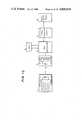
- the variant shown in FIG. 15relates to a set comprising reproducer means for the reproduction of alphanumerical data, on a display screen, or reproducer printing means or vocal reproducer means, and in respect of the block diagram shown in FIG. 1 there is missing the frequency-synthesis PLL circuit 8.
- the circuit 4(which is a known circuit for the reproducer means 5) receives the signals from the unit 3 and generates the pilot control signals for the reproducer means 5 which reproduce on a screen, or printing reproducers (typewriter or printing machine) or vocal reproducers (reproducing the single character or also the combination of characters), so as to obtain the 64 types of alphanumerical characters corresponding to the 64 keys which may be selected by means of the keyboard of the transmitter 1.
- the apparatus shown in FIG. 1may be used for different functions, including also the note-book function for memorizing determined data and reproducing them at the desired moment, or the calendar function for obtaining data of the type described already in the foregoing, with the advantage of having the control keyboard 1 freely movable, without it having to be constrained to a fixed and limited position relative to the set.
Landscapes
- Engineering & Computer Science (AREA)
- Computer Hardware Design (AREA)
- Microelectronics & Electronic Packaging (AREA)
- Physics & Mathematics (AREA)
- General Physics & Mathematics (AREA)
- Theoretical Computer Science (AREA)
- Controls And Circuits For Display Device (AREA)
Abstract
Description
"CALENDAR OF ??/????"
______________________________________ DECEMBER 1980 MO TU WE TH FR SA SU ______________________________________ 1 2 3 4 5 6 7 8 9 10 11 12 13 14 15 16 17 18 19 20 21 22 23 24 25 26 27 28 29 30 31 ______________________________________
NN/MM
TABLE 1 ______________________________________ ADDRESS CODE ______________________________________ M0000 = 1A 70 B4 62 6C 5C 52 2A M0008 = 0F C0 20 E0 17 71 17 7D M0010 = 58 20 F0 17 38 94 FD 20 M0018 = 10 B1 6F 5C 65 6D 5C 20 M0020 = AA B6 2A 0F FF 20 34 17 M0028 = 20 3C 53 43 25 3C 84 01 M0030 = 20 A0 67 6F 5E 5D 28 00 M0038 = D7 94 19 2A 0F FF 16 25 M0040 = 33 94 E9 43 25 2B 94 E4 M0048 = 1A 3C 94 EB 4E 3D 94 E7 M0050 = 29 02 B8 20 BB B7 28 00 M0058 = D7 94 FC 1A A7 91 D8 71 M0060 = 5A 20 3F 0B 70 5E 5C 59 M0068 = 20 A0 B7 28 00 D7 4B E9 M0070 = 84 FA 4B 59 70 CB 84 04 M0078 = 4A CC 5C 4A 13 5A 84 0C M0080 = 25 10 94 0B 0A 25 3F 84 M0088 = 0E 90 04 71 5A 4D A7 91 M0090 = D8 20 FF B7 90 DF 20 3E M0098 = 0B 70 59 71 5A 25 10 94 M00A0 = 05 4D 4C 15 5C 4C 12 5C M00A8 = FA C9 59 4A 13 5A 81 EE M00B0 = 49 25 3E 84 05 53 29 00 M00B8 = 30 43 25 31 81 05 2A 0F M00C0 = FF 17 2A 0F FF 16 25 33 M00C8 = 84 06 92 07 29 01 3B 29 M00D0 = 00 DF 43 52 29 09 1C 70 M00D8 = B0 A0 18 21 01 5B 1C ______________________________________
TABLE 2 ______________________________________ ADDRESS CODE ______________________________________ M0138 = 43 25 32 84 4A M0140 = 25 30 84 6C 70 C8 84 05 M0148 = 25 30 94 3E 45 15 13 C2 M0150 = 18 07 43 25 20 81 50 25 M0158 = 2E 84 1B 25 2F 84 2D 25 M0160 = 2A 84 42 25 29 84 2B 25 M0168 = 2B 84 3E 25 2D 84 07 40 M0170 = 24 40 50 90 1B 20 20 59 M0178 = 28 02 A6 32 81 F8 43 25 M0180 = 2D 94 26 35 20 1F 52 81 M0188 = ED 90 51 48 23 30 58 90 M0190 = 65 42 24 02 25 1F 81 0C M0198 = 70 52 28 02 5B 45 1F 21 M01A0 = 07 55 72 52 90 5D 90 50 M01A8 = 70 52 28 02 5B 90 5A 38 M01B0 = 77 55 70 52 2A 05 7F 48 M01B8 = 21 01 94 15 20 1E 59 20 M01C0 = 20 2A 0F DF 17 17 42 17 M01C8 = 1F 52 39 94 FA 2A 0F DF M01D0 = 20 20 59 28 02 8F 35 81 M01D8 = DF 90 37 70 58 52 07 20 M01E0 = 20 59 28 02 A6 76 55 28 M01E8 = 02 5B 35 81 FB 20 C0 50 M01F0 = 20 1E 52 77 55 90 18 43 M01F8 = 25 20 84 03 C0 E8 59 28 M0200 = 02 A6 32 94 0A 28 02 5B M0208 = 20 1E 52 35 91 E6 28 02 M0210 = 5B 29 00 2B 07 12 E0 E0 M0218 = C3 C1 CC C5 CE C4 C1 D2 M0220 = C9 CF E0 C4 C5 CC FA E0 M0228 = 07 08 16 59 70 55 22 10 M0230 = B1 28 02 4F 94 FC 16 59 M0238 = 0F 28 02 4F 94 FC 2A 02 M0240 = 14 16 59 20 20 18 B4 28 M0248 = 02 52 94 F8 70 B1 0C 16 M0250 = 18 B4 45 22 18 B1 23 08 M0258 = B1 39 1C 2A 0F DF 20 20 M0260 = 59 45 18 15 13 1F 07 20 M0268 = 27 B1 20 20 90 1B 49 25 M0270 = 1F 84 F8 03 B5 1F 07 70 M0278 = B4 A4 64 6F 5C 49 E2 4C M0280 = 94 07 48 14 12 C0 24 1E M0288 = 17 39 94 E3 2A 0F DF 08 M0290 = 77 B1 A0 21 10 94 FC 20 M0298 = 20 59 45 22 10 B1 28 02 M02A0 = 4F 94 FC 77 B1 0C A1 22 M02A8 = 20 B1 03 B5 1F 07 49 B4 M02B0 = A1 23 08 B1 23 28 B1 1C ______________________________________
TABLE 3 ______________________________________ ADDRESS CODE ______________________________________ M00D8 66 M00E0 = 43 25 33 94 226D 20 80 M00E8 = 582A 0F DF 77 59 20 3F M00F0 = 22 40 17 39 94 FD 2A 0F M00F8 =E1 202F 22 40 17 70 52 M0100 = 2A0F DF 0E 90 22 40 0B M0108 =0F 42 25 02 94 02 1F 8E M0110 =1F 52 43 22 30 22 40 17 M0118 =C8 91 09 21 0FCC 5D 20 M0120 = 80 90 04 155C 70 58 2A M0128 = 02 15 28 02 290A 50 24 M0130 =F8 21 07 94 04 29 02 B8 M0138 = 29 00 2B ______________________________________
TABLE 4 ______________________________________ ADDRESS CODE ______________________________________ M02B8 = 90 17 71 90 10 20 12 90 M02C0 = 0C 20 24 5D 20 99 90 05 M02C8 = 20 16 5D 70 5C 28 05 00 M02D0 = 66 6D 4C 25 00 82 E4 25 M02D8 = 12 92 E3 4D 4C 25 24 92 M02E0 = E1 25 15 82 E4 6C 4D 4C M02E8 = 21 0F 58 4E 14 13 59 13 M02F0 = 13 C9 C8 58 4E 4E 48 5D M02F8 = 4D 4D 8F EB 2A 05 9B 6A M0300 = 4D 5A 4C 8E 13 13 CD CC M0308 = 24 ED 82 FD 24 13 67 6A M0310 = 5C 20 13 59 16 CC 25 1D M0318 = 82 03 24 E2 39 94 F7 69 M0320 = 5C 13 CC 58 66 6C 4C 21 M0328 = 03 C8 58 4E CC CC 24 F9 M0330 = 82 FD 24 OA 13 C8 13 58 M0338 = 4C 12 12 18 CC C8 24 F9 M0340 = 82 FD 24 07 67 68 5C 24 M0348 = 16 69 CC 58 59 25 1E 81 M0350 = 1D 24 E1 59 25 19 91 0F M0358 = 94 11 68 4C 25 06 94 0B M0360 = 6A 4C 25 0A 81 05 49 24 M0368 = F9 59 74 90 02 73 EA 70 M0370 = 5B 94 08 20 67 DB 5B 39 M0378 = 81 FA 2A 05 B3 4A 8E 48 M0380 = 18 24 3C 88 58 70 59 66 M0388 = 6C 4C 21 03 94 12 CE 94 M0390 = 06 4C 21 03 94 0A 4E 4C M0398 = 25 02 91 04 38 71 59 6C M03A0 = 67 48 24 F9 81 FD 24 07 M03A8 = 13 13 5C 70 55 65 6F 5E M03B0 = 8F FE 28 02 5B 2A 0F E1 M03B8 = 0E 03 24 00 81 2F 16 21 M03C0 = 3F 25 2F 94 F4 16 21 0F M03C8 = 13 5C 13 13 CC 5C 16 21 M03D0 = 0F CC 18 1F CA 94 E2 20 M03D8 = FB 8E 16 21 0F 13 5C 13 M03E0 = 13 CC 5C 16 21 0F CC 5D M03E8 = 73 8E 90 CD M0528 = D3 47 45 4E 4E M0530 = 06 80 46 45 42 42 52 41 M0538 = 49 4F 83 4D 41 52 5A 4F M0540 = 82 41 50 52 49 4C 45 D3 M0548 = 4D 41 47 47 49 4F 82 47 M0550 = 49 55 47 4E 4F 83 4C 55 M0558 = 47 4C 49 4F B3 41 47 4F M0560 = 53 54 4F 82 53 45 54 54 M0568 = 0F 83 4F 54 54 4F 0B D2 M0570 = 4E 4F 56 04 C3 44 49 43 M0578 = 45 4D 42 52 45 80 4C 55 M0580 = 4D 41 4D 45 47 49 56 45 M0588 = 53 41 44 4F 71 F2 F3 F4 M0590 = F5 F6 F7 78 F9 90 91 92 M0598 = 93 94 15 96 97 98 99 A0 M05A0 = A1 A2 A3 A4 25 26 A7 A8 M05A8 = A9 B0 B1 16 17 17 18 18 M05B0 = 18 19 1A 19 01 04 04 00 M05B8 = 02 05 00 03 06 01 04 06 ______________________________________
TABLE 5 ______________________________________ ADDRESS CODE ______________________________________ M03E8 = 20 40 50 77 M03F0 = 55 B1 2A 05 2B 45 22 10 M03F8 = B1 20 1F 52 49 25 02 84 M0400 = 70 28 05 1C 42 25 1B 91 M0408 = F9 45 25 07 84 25 25 05 M0410 = 94 06 6C 67 3C 81 EB 16 M0418 = 56 45 25 06 42 94 54 25 M0420 = 04 20 80 91 03 20 00 50 M0428 = 28 05 16 16 56 28 05 16 M0430 = 90 7D 42 25 16 91 CB 70 M0438 = 88 81 FD 3A 94 FA 5A 21 M0440 = 0F 94 02 C9 59 20 8E D9 M0448 = 59 16 25 1F 81 06 56 28 M0450 = 05 16 70 8E 70 88 81 F3 M0458 = 28 05 1C 42 25 0A 91 F9 M0460 = 6E 66 4D 58 28 05 01 4E M0468 = 58 2A 05 7E 90 73 90 86 M0470 = 90 72 25 04 81 32 46 21 M0478 = 7F 25 70 82 03 21 0F EB M0480 = 84 26 46 21 1F 65 68 EE M0488 = 84 05 8F FC 90 05 20 40 M0490 = 90 3D 70 C6 91 37 4A 14 M0498 = 21 07 E5 84 1D 4A 25 C3 M04A0 = 94 2B 45 25 02 91 26 20 M04A8 = 00 90 24 28 05 01 28 05 M04B0 = 1C 28 05 1C 91 33 29 04 M04B8 = 17 6D 66 4D 25 05 94 E8 M04C0 = 4D 25 18 92 E3 94 06 4E M04C8 = 25 89 92 DC 20 C0 50 46 M04D0 = 22 80 56 21 40 46 94 03 M04D8 = 21 7F 58 E9 94 CE 72 59 M04E0 = 28 05 01 28 05 1C 81 FC M04E8 = 77 B1 35 81 82 6D 66 4C M04F0 = 25 12 94 04 71 5D 4D 20 M0458 = 67 DC 5E 84 FB 29 00 2B M0500 = 1C 08 48 14 25 0F 94 02 M0508 = 15 24 30 56 28 05 16 48 M0510 = 21 0F 24 30 56 09 46 21 M0518 = 3F C0 90 05 20 20 56 46 M0520 = 18 B4 45 22 18 B1 23 08 M0528 = B1 32 1C ______________________________________
______________________________________ P3 CHANNEL 42 KEY6 GRP ______________________________________
______________________________________ C 21 30 42 22 35 61 ?? ?? ?? P3 ______________________________________
______________________________________ P3 CHANNEL 42 KEY6 G?? ______________________________________
______________________________________ P1Λ CHANNEL 54 KEYG?? ______________________________________
______________________________________ 0-9 Selection of one of the 10 programs stored on the current memory page, or direct selection of 99 channels by pressing two numbers in less than one second. <e> Tuning correction. MEM Memory map display and (second time pressed) memorization setting. VOL, LUM, Volume, brightness and color saturation SAT adjustment. R1, R2, R3 Buttons for starting three types of memorized programme or channel scanning operations. PAG Page number forward key. ______________________________________
TABLE 6 ______________________________________ ADDRESS CODE ______________________________________ M08D0 = 2A 0F D6 M08D8 = 20 30 17 17 17 28 08 39 M08E0 = 28 08 71 2A 0F D6 73 5C M08E8 = 20 31 58 7F 90 AB 28 09 M08F0 = 01 4C 25 06 94 A6 28 08 M08F8 = 39 70 57 58 2A 0F CA 90 M0900 = 96 2A 0F CA 16 25 F0 70 M0908 = 94 03 20 30 50 2A 0F D3 M0910 = 65 6E 4C 8E 1F 5C 43 E0 M0918 = 24 10 17 1C 2A 0F CA 43 M0920 = 25 34 94 35 28 0D 69 78 M0928 = 8E 7F 8D 94 16 65 6A 4C M0930 = 90 1E 2A 0F CD 8D 94 14 M0938 = 70 C1 81 19 21 0F 57 29 M0940 = 09 EC 2A 0F D8 8D 94 EB M0948 = 28 0D 71 2A 0F D4 16 25 M0950 = 09 82 EC 41 59 29 09 DF M0958 = 25 2F 84 33 25 2C 84 29 M0960 = 25 30 84 4C 5B 48 25 31 M0968 = 94 04 29 08 EE 25 30 84 M0970 = 1B 4B 25 13 84 3A 2A 0F M0978 = CB 25 09 81 24 25 17 81 M0980 = 2F 25 1D 91 2B 29 07 41 M0988 = 29 06 D1 29 08 7E 16 25 M0990 = EE 2A 0F CA 84 05 20 EE M0998 = 90 03 20 F0 17 29 0C 50 M09A0 = 5B 47 56 17 4B 57 17 7F M09A8 = E6 84 13 70 58 90 0F 25 M09B0 = 0E 91 08 25 0B 81 04 29 M09B8 = 0B 37 58 7F 57 48 2A 0F M09C0 = CB 25 13 84 0E 81 26 25 M09C8 = 30 84 C1 25 16 91 1E 29 M09D0 = 06 F9 29 0A 5C ______________________________________
TABLE 7 ______________________________________ ADDRESS CODE ______________________________________ M0A58 = 7F E7 84 07 M0A60 = 70 C5 94 89 90 6F 55 16 M0A68 = 25 DD 94 18 28 0D 71 2A M0A70 = 0F CD 7F 8D 94 07 28 0D M0A78 = 63 29 0B 64 2A 0F CC 17 M0A80 = 29 0C 4B 20 FF 55 2A 0F M0A88 = CB 20 DD 17 20 F0 17 20 M0A90 = 20 63 6C 5C A1 22 40 B1 M0A98 = 79 57 50 28 07 B8 28 08 M0AA0 = 17 47 24 1D 0B 70 C6 94 M0AA8 = 03 20 FF 81 02 30 5C 37 M0AB0 = 81 EA 70 57 28 08 01 24 M0AB8 = 33 B5 A4 E0 84 0F 70 CC M0AC0 = 81 04 20 92 5C 0A 1F 0B M0AC8 = 25 27 94 F3 28 08 54 7F M0AD0 = 57 29 0C 59 2A 0F D3 20 M0AD8 = F0 17 47 17 76 5B 79 50 M0AE0 = 47 24 1D 0B 41 5C 63 6D M0AE8 = 70 CC 81 02 30 0A 1F 0B M0AF0 = 25 27 94 F5 28 08 01 62 M0AF8 = 6B 4E B4 23 80 B4 23 80 M0B00 = B4 4A 1F B5 5A 8F 0A 60 M0B08 = 69 20 FF 8E 16 24 32 5A M0B10 = 4E 3B 94 E7 70 B4 28 08 M0B18 = 54 48 25 13 94 47 29 08 M0B20 = D5 M07B8 = 08 28 08 01 62 6B 3A 90 M07C0 = 03 5C 4E 4A 1F 5A B5 48 M07C8 = 25 13 94 04 A4 8F F4 A4 M07D0 = 8F F0 56 28 08 54 46 21 M07D8 = 0F 25 09 91 0F 6B 4E 25 M07E0 = 20 92 09 4E 25 64 92 04 M07E8 = 8F FA 0C 20 FF 56 0C M07F8 = 00 34 M0800 = 68 A1 23 80 B1 47 13 13 M0808 = C7 5A 2A 0F C1 16 2A 07 M0810 = FD 8E 16 CA 5A B5 1C 08 M0818 = 2A 0F C1 16 59 08 28 08 M0820 = 5B A4 25 10 82 0F 25 49 M0828 = 92 0B 17 4A 1F 5A B5 3B M0830 = 94 F0 90 04 20 FF 56 90 M0838 = 1B 08 2A 0F C1 16 59 28 M0840 = 08 5B 16 21 7F B4 23 80 M0848 = B4 23 80 B4 4A 1F 5A B5 M0850 = 3B 94 F0 09 70 B5 A1 23 M0858 = 80 B1 1C A1 23 80 B1 73 M0860 = 5B 47 13 C7 24 7C 5A 49 M0868 = 15 13 CA 5A B5 2A 0F D6 M0870 = 1C ______________________________________
TABLE 8 ______________________________________ ADDRESS CODE ______________________________________ M09E8 = 70 58 55 C7 M09F0 = 84 09 2A 0F CA 16 25 EE M09F8 = 84 DC 2A 0F D4 16 25 09 M0A00 = 92 04 22 80 51 43 25 09 M0A08 = 91 13 656D 4C 25 03 92 M0A10 =0A 25 01 73 5E5D 94 C1 M0A18 = 90 03 71 5C 2A 0F CD 7C M0A20 =5A 20 F0 173A 94FD 28 M0A28 = 07 B8 2A 0F D4 47 17 28 M0A30 = 08 17 46 59 25FF 94 09 M0A38 = 28 07EF 280D 3E 90 1A M0A40 = 2A 0F D6 16 25 56 94 0C M0A48 = 16 25 43 94 07A1 22 10 M0A50 =B1 90 07A1 22 10 23 10 MOA58 =B1 290B 70 MOB20 = 7F 2A 0F CD 17 17 2A M0B28 =0F D4 70 88 280D 71 81 M0B30 = 04 280D 63 29 0C 4B ______________________________________
TABLE 9 ______________________________________ ADDRESS CODE ______________________________________ M0878 = 43 25 M0880 = 30 941C 28 08 71 70 5C M0888 = 55 2A 0F D4 16 6A 5C 2A M0890 = 0F D3 7F 17 17 17 20 F0 M0898 = 17 17 17 29 0C4B 28 09 M08A0 = 014C 25 03 94 F6 73 59 M08A8 = 79 57 28 08 1D 73 5A 2A M08B0 = 0F D2 4A 8E 16 8D 8D 8D M08B8 = 94 143A 94 F3 2A 0F CA M08C0 = 20 F0 172A 0F C1 49 17 M08C8 = 70 58 29 09FA 37 81 DB M08D0 = 39 94D6 90 AF ______________________________________
TABLE 10 ______________________________________ AD- ASSEM- DRESS CODE BLER ______________________________________ START RORG 0 ENTRY LOOP EXTRN CALE,CALEN, STAR,TACC 0000 1A DI 0001 70 CLR 0002 B4 OUTS DOP 0003 62 LISU VEN 0004 6C LISL VAR 0005 5C LR S,A 0006 52 LR RIF,A 0007 2A0FC0 DCI BUF 000A 20E0 LI H`EO` 000C 17 ST 000D 71 LIS 1 000E 17 ST 000F 7D LIS 13 0010 58 LR MOO,A 0011 20F0 LI H`FO` 0013 17 ST 0014 38 DS MOO 0015 94FD BNZ *-2 0017 2010 LI H`10` 0019 B1 OUTS S2P 001A 6F LISL FMU 001B 5C LR S,A 001C 65 LISU 5 001D 6D LISL 5 001E 5C LR S,A 001F 20AA LI H`AA` 0021 B6 OUTS 6 0022 2A0FFF DCI FUNZ 0025 2034 LI NOR 0027 17 ST 0028 203C LI 60 002A 53 LR TAS,A 002B 43 LOOP LR A,TAS 002C 253C CI 60 002E 8401 BZ INIZ 0030 20A0 INIZ LI 160 0032 67 LISU TIME 0033 6F LISL TIME 0034 5E LR D,A 0035 5D LR I,A 0036 2800D7 IZZ PI INPUT 0039 9419 BNZ STA1 003B 2A0FFF DCI FUNZ 003E 16 LM 003F 2533 CI 51 0041 94E9 BNZ LOOP 0043 43 LR A,DAT 0044 252B CI CROT 0046 94E4 BNZ LOOP 0048 1A DI 0049 3C DS S 004A 94EB BNZ IZZ 004C 4E LR A,D 004D 3D DS I 004E 94E7 BNZ IZZ 0050 290000 JMP CALEN 0053 20BB STA1 LI H`BB` 0055 B7 OUTS 7 0056 2800D7 STARTB PI INPUT 0059 94FC BNZ STARTB 005B 1A DI 005C A7 INS 7 005D 91D8 BM IZZ 005F 71 LIS 1 0060 5A LR MASK,A 0061 203F LI BMS+ 1 0063 0B LR IS,A 0064 70 CLR 0065 5E LR D,A 0066 5C LR S,A 0067 59 LR TEM,A 0068 20A0 RD1 LI H`A0` 006A B7 OUTS 7 006B 2800D7 REA PI INPUT 006E 4B LR A,CON 006F E9 XS TEM 0070 84FA BZ REA 0072 4B LR A,CON 0073 59 LR TEM,A 0074 70 D2 CLR 0075 CB AS CON 0076 8404 BZ ZERO 0078 4A LR A,MASK 0079 CC AS S 007A 5C LR S,A 007B 4A ZERO LR A,MASK 007C 13 SL 1 007D 5A LR MASK,A 007E 840C BZ T1 0080 2510 CI B`10000` 0082 940B BNZ TEMPO 0084 0A LR A,IS 0085 253F CI BMS+1 0087 840E BZ END 0089 9004 BR TEMPO 008B 71 T1 LIS 1 008C 5A LR MASK,A 008D 4D LR A,I 008E A7 TEMPO INS 7 008F 91D8 BM RD1 0091 20FF LI H`FF` 0093 B7 OUTS 7 0094 90DF BR D2 0096 203E END LI BMS 0098 0B LR IS,A 0099 70 CLR 009A 59 LR TEM,A 009B 71 LIS 1 009C 5A LR MASK,A 009D 2510 BIT1 CI B`10000` 009F 9405 BNZ BIT 00A1 4D LR A,I 00A2 4C LR A,S 00A3 15 SL 4 00A4 5C LR S,A 00A5 4C BIT LR A,S 00A6 12 SR 1 00A7 5C LR S,A 00A8 FA NS MASK 00A9 C9 AS TEM 00AA 59 LR TEM,A 00AB 4A LR A,MASK 00AC 13 SL 1 00AD 5A LR MASK,A 00AE 81EE BP BIT 1 00B0 49 LR A,TEM 00B1 253E CI H`3E` 00B3 8405 BZ TEST 00B5 53 LR DAT,A C0B6 290030 JMP INIZ 00B9 43 TEST LR A,DAT 00BA 2531 CI 49 00BC 8105 BP TE 00BE 2A0FFF DCI FUNZ 00C1 17 ST 00C2 2A0FFF TE DCI FUNZ 00C5 16 LM 00C6 2533 CI 51 00C8 8406 BZ C 00CA 9207 BNC D 00CC 290000 JMP TACC 00CF 290000 C JMP CALE 00D2 43 D LR A,TAS 00D3 52 LR RIF,A 00D4 290000 JMP STAR 00D7 70 INPUT CLR 00D8 B0 OUTS IN 00D9 A0 INS IN 00DA 18 COM 00DB 2101 NI TC 00DD 5B LR CON,A CODE 1C POP END ______________________________________
TABLE 11 ______________________________________ ADDRESS CODE ASSEMBLER ______________________________________ 005C 43 TACC LR A,DAT 005D 2532 CI TAC 005F 844A BZ TC2 0061 2530 CI RAND 0063 846C BZ RDM 0065 70 CLR 0066 C8 AS FLA 0067 8405 BZ TA 0069 2530 CI H`30` 006B 943E BNZ TC2 006D 45 TA LR A,ADD 006E 15 SL 4 006F 13 SL 1 0070 C2 AS CRT 0071 18 COM 0072 07 LR QL,A 0073 43 LR A,DAT 0074 2520 CI 32 0076 8150 BP W44 0078 252E CI RETURN 007A 841B BZ RET 007C 252F CI SHIFT 007E 842D BZ SHI 0080 252A CI PFOR 0082 8442 BZ W41 0084 2529 CI PBAK 0086 842B BZ PB 0088 252B CI PDOW 008A 843E BZ PD 008C 252D CI CLEAR 008E 8407 BZ RET 0090 40 LR A,COL 0091 2440 AI H`40` 0093 50 LR COL,A 0094 901B BR W50 0096 2020 RET LI C` ` 0098 59 LR TEM,A 0099 2801C7 PI STO 009C 32 DS CRT 009D 81F8 BP RET 009F 43 LR A,DAT 00A0 252D CI CLEAR 00A2 9426 BNZ PD 00A4 35 DS ADD 00A5 201F LI 31 0047 52 LR CRT,A 00A8 81ED BP RET 00AA 9051 TC2 BR TC1 00AC 48 SHI LR A,FLA 00AD 2330 XI F2 00AF 58 LR FLA,A 00B0 9065 W50 BR W11 00B2 42 PB LR A,CRT 00B3 2402 AI 2 00B5 251F CI 31 00B7 810C BP PB1 00B9 70 LIS O 00BA 52 LR CRT,A 00BB 28017C PI OUTL 00BE 45 LR A,ADD 00BF 1F INC 00C0 2107 NI 7 00C2 55 LR ADD,A 00C3 72 LIS 2 00C4 52 PB1 LR CRT,A 00C5 905D W41 BR W4 00C7 9050 W44 BR WRT 00C9 70 PD LIS O 00CA 52 LR CRT,A 00CB 28017C PI OUTL 00CE 905A BR W3 00D0 38 RDM DS FLA 00D1 77 LIS 7 00D2 55 LR ADD,A 00D3 70 CLR 00D4 52 LR CRT,A 00D5 2A057F DCI MESS 00D8 48 RM1 LR A,FLA 00D9 2101 NI 1 00DB 9415 BNZ RM5 00DD 201E LI 30 00DF 59 LR TEM,A 00E0 2020 LI C` ` 00E2 2A0FDF DCI DATA 00E5 17 ST 00E6 17 ST 00E7 42 RM3 LR A,CRT 00E8 17 ST 00E9 1F INC 00EA 52 LR CRT,A 00EB 39 DS TEM 00EC 94FA BNZ RM3 00EE 2A0FDF DCI DATA 00F1 2020 RM5 LI 32 00F3 59 LR TEM,A 00F4 2801B0 PI 022 00F7 35 DS ADD 00F8 81DF BP RM1 00FA 9037 BR W2 00FC 70 TC1 CLR 00FD 58 LR FLA,A 00FE 52 LR CRT,A 00FF 07 LR QL,A 0100 2020 LI C` ` 0102 59 LR TEM,A 0103 2801C7 PI STO 0106 76 LIS 6 0107 55 LR ADD,A 0108 28017C OL PI OUTL 010B 35 DS ADD 010C 81FB BP OL 010E 20C0 LI BIANCO 0110 50 LR COL,A 0111 201E LI 30 0113 52 LR CRT,A 0114 77 PL LIS 7 0115 55 LR ADD,A 0116 9018 W11 BR W1 0118 43 WRT LR A,DAT 0119 2520 CI C` ` 011B 8403 BZ W5 011D C0 AS COL 011E E8 XS FLA 011F 59 W5 LR TEM,A 0120 2801C7 PI STO 0123 32 W4 DS CRT 0124 940A BNZ W1 0126 28017C PI OUTL 0129 201E W3 LI 30 012B 52 LR CRT,A 012C 35 DS ADD 012D 91E6 BM PL 012F 28017C W1 PI OUTL 0132 290000 W2 IMP LOOP 017C 2AOFDF OUTL DC1 DATA 017F 2020 LI 32 0181 59 LR TEM,A 0182 45 LR A,ADD 0183 18 COM 0184 15 SL 4 0185 13 SL 1 0186 1F INC 0187 07 LR QL,A 0188 2027 LI CSE+ 7 018A B1 OUTS S2P 018B 2020 BLK LI C` ` 018D 901B BR 02 018F 49 03 LR A,TEM 0190 251F CI 31 0192 84F8 BZ BLK 0194 03 LR A,QL 0195 B5 OUTS TIP 0196 1F INC 0197 07 LR QL,A 0198 70 CLR 0199 B4 OUTS DOP 019A A4 INS DOP 019B 64 LISU 4 019C 6F LISL 7 019D 5C LR S,A 019E 49 LR A,TEM 019F E2 XS CRT 01A0 4C LR A,S 01A1 9407 BNZ 02 01A3 48 LR A,FLA 01A4 14 SR 4 01A5 12 SR 1 01A6 C0 AS COL 01A7 241E AI PUNT-1 01A9 17 02 ST 01AA 39 DS TEM 01AB 94E3 BNZ 03 01AD 2A0FDF DCI DATA 01B0 08 022 LR K,P 01B1 77 LIS 7 01B2 B1 OUTS S2P 01B3 A0 INS O 01B4 2110 NI RS 01B6 94FC BNZ *-3 01B8 2020 LI 32 01BA 59 LR TEM,A 01BB 45 LR A,ADD 01BC 2210 OI DT 01BE B1 OUTS S2P 01BF 280170 033 PI DCL 01C2 94FC BNZ 033 01C4 77 LIS 7 01C5 B1 OUTS S2P 01C6 OC PK 01C7 A1 STO INS S2P 01C8 2220 OI CSE 01CA B1 OUTS S2P 01CB 03 LR A,QL 01CC B5 OUTS TIP 01CD 1F INC 01CE 07 LR QL,A 01CF 49 LR A,TEM 01D0 B4 OUTS DOP 01D1 A1 INS S2P 01D2 2308 XI DC 01D4 B1 OUTS S2P 01D5 2328 XI DC+ CSE 01D7 B1 OUTS S2P 01D8 1C POP END ______________________________________
TABLE 12 ______________________________________ AD- DRESS CODE ASSEMBLER ______________________________________ CALE RORG O ENTRY TACC,OUTL EXTRN LOOP,CALEN 0000 66 LISU DATE 0001 43 LR A,DAT 0002 2533 CI CAL 0004 9422 BNZ CX 0006 6D LISL ANN-2 0007 2080 LI F1 0009 58 LR FLA,A 000A 2A0FDF DCI DATA 000B 77 LIS 7 000E 59 LR TEM,A 000F 203F LI C`?` 0011 2240 OI GIALLO 0013 17 ST1 ST 0014 39 DS TEM 0015 94FD BNZ ST1 0017 2A0FE1 DCI DATA+2 001A 202F LI C`1` 001C 2240 OI GIALLO 001E 17 ST 001F 70 CLR 0020 52 LR CRT,A 0021 2A0FDF DCI DATA 0024 0E LR Q,DC 0025 9022 BR DC2 0027 40 CX LR A,COL 0028 0B LR IS,A 0029 0F LR DC,Q 002A 42 LR A,CRT 002B 2502 CI 2 002D 9402 BNZ CX1 002F 1F INC 0030 8E CX1 ADC 0031 1F INC 0032 52 LR CRT,A 0033 43 LR A,DAT 0034 2230 OI H`30` 0036 2240 OI GIALLO 0038 17 ST 0039 C8 AS FLA 003A 9109 BM DEC 003C 210F NI H`F` 003E CC AS S 003F 5D LR I,A 0040 2080 LI F1 0042 9004 BR DC1 0044 15 DEC SL 4 0045 5C LR S,A 0046 70 CLR 0047 58 DC1 LR FLA,A 0048 2A0136 DC2 DCI CLD 004B 28014A PI OUTL1 004E 0A LR A,IS 004F 50 LR COL,A 0050 24F8 AI -(ANN+1) 0052 2107 NI 7 0054 9404 BNZ IN 0056 290000 JMP CALEN 0059 290000 IN JMP LOOP ______________________________________
TABLE 13 ______________________________________ ADDRESS CODE ASSEMBLER ______________________________________ CALEN RORG O ENTRY FINE EXTERN LOOP, OUTL 0000 9017 BR START 0002 71 ERR1 LIS 1 0003 9010 BR ERROR 0005 2012 ERR2 LI H`12` 0007 900C BR ERROR 0009 2024 ERR3 LI H`24` 000B 5D LR I,A 000C 2099 LI H`99` 000E 9005 BR ERROR 0010 2016 ERR4 LI H`16` 0012 5D LR I,A 0013 70 CLR 0014 5C ERROR LR S,A 0015 280248 PI BEEP 0018 66 START LISU DATE 0019 6D LISL ANN-2 001A 4C LR A,S 001B 2500 CI O 001D 82E4 BC ERR1 001F 2512 CI H`12` 0021 92E3 BNC ERR2 0023 4D LR A,1 0024 4C LR A,S 0025 2524 CI H`24` 0027 92E1 BNC ERR3 0029 2515 CI H`15` 002B 82E4 BC ERR4 002D 6C LISL ANN-3 002E 4D BIN LR A,I 002F 4C LR A,S 0030 210F NI H`E` 0032 58 LR TE2,A 0033 4E LR A,D 0034 14 SR 4 0035 13 SL 1 0036 59 LR TE1,A 0037 13 SL 1 0038 13 SL 1 0039 C9 AS TE1 003A C8 AS TE2 003B 58 LR TE2,A 003C 4E LR A,D 003D 4E LR A,D 003E 48 LR A,TE2 003F 5D LR I,A 0040 4D LR A,I 0041 4D LR A,I 0042 8FEB BR7 BIN 0044 2A02E3 DCI EMME-16 0047 6A LISL ANN-5 0048 4D LR A,I 0049 5A LR MES,A 004A 4C LR A,S 00AB 8E ADC 004C 13 SL 1 004D 13 SL 1 004E CD AS I 004F CC AS S 0050 24ED FO AI -19 0052 82FD BC FO 0054 2413 AI 19 0056 67 LISU MODU 0057 6A LISL C 0058 5C LR S,A 0059 2013 LI 19 005B 59 LR TE1,A 005C 16 LM 005D CC AS AS S 005E 215D CI 29 0060 8203 BC F1 0062 24E2 AI -30 0064 39 F1 DS TE1 0065 94F7 BNZ AS 0067 69 LISL D 0068 5C LR S,A 0069 13 SL 1 006A CC AS S 006B 58 LR TE2,A 006C 66 LISU DATE 006D 6C LISL ANN-3 006E 4C LR A,S 006F 2103 NI 3 0071 C8 AS TE2 0072 58 LR TE2,A 0073 4E LR A,D 0074 CC AS S 0075 CC AS S 0076 24F9 F2 AI -7 0078 82FD BC F2 007A 240A AI 10 007C 13 SL 1 007D C8 AS TE2 007E 13 SL 1 007F 58 LR TE2,A 0080 4C LR A,S 0081 12 SR 1 0082 12 SR 1 0083 18 COM 0084 CC AS S 0085 C8 AS TE2 0086 24F9 F3 AI -7 0088 82FD BC F3 008A 2407 AI 7 008C 67 LISU MODU 008D 68 LISL E 008E 5C LR S,A 008F 2416 AI 22 0091 69 LISL D 0092 CC AS S 0093 58 LR TE2,A 0094 59 LR TE1,A 0095 251E CI 30 0097 811D BP MARZ 0099 24EI AI -31 009B 59 LR TE1,A 009C 2519 CI 25 009E 910F BM AP2 00A0 9411 BNZ APRIL 00A2 68 LISL E 00A3 4C LR A,S 00A4 2506 CI 6 00A6 940B BNZ APRIL 00A8 6A LISL C 00A9 4C LR A,S 00AA 250A CI 10 00AC 8105 BP APRIL 00AE 49 AP2 LR A,TE1 00AF 24F9 AI -7 00B1 59 LR TE1,A 00B2 74 APRIL LIS 4 00B3 9002 BR MA1 00B5 73 MARZ LIS 3 00B6 EA MA1 XS MES 00B7 70 CLR 00B8 5B LR GIO,A 00B9 9408 BNZ PMES 00BB 2067 BCD LI H`67` 00BD DB ASD GIO 00BE 5B LR GIO,A 00BF 39 DS TE1 00C0 81FA BP BCD 00C2 2A02FB PMES DCI ESSE-1 00C5 4A LR A,MES 00C6 8E ADC 00C7 48 LR A,TE2 00C8 18 COM 00C9 243C AI 60 00CB 88 AM 00CC 58 LR TE2,A 00CD 70 CLR 00CE 59 LR TE1,A 00CF 66 LISU DATE 00D0 6C LISL ANN-3 00D1 4C LR A,S 00D2 2103 NI 3 00D4 9412 BNZ NORM 00D6 CE AS D 00D7 9406 BNZ BIS 00D9 4C LR A,S 00DA 2103 NI 3 00DC 940A BNZ NORM 00DE 4E BIS LR A,D 00DF 4C LR A,S 00E0 2502 CI 2 00E2 9104 BM NORM 00E4 38 DS TE2 00E5 71 LIS 1 00E6 59 LR TE1,A 00E7 6C NORM LISL A 00E8 67 LISU MODU 00E9 48 LR A,TE2 00EA 24F9 NI AI -7 00EC 81FD BP N1 00EE 2407 AI 7 00F0 13 SL 1 00F1 13 SL 1 00F2 5C LR S,A 00F3 70 CLR 00F4 55 LR ADD,A 00F5 65 LISU 5 00F6 6F LISL 7 00F7 5E LR D,A 00F8 8FFE BR7 *-1 00FA 280000 PI OUTL 00FD 2A0FE1 DCI DATA+2 0100 0E LLMM LR Q,DC 0101 03 LR A,QL 0102 2400 AI O 0104 812F BP DSC 0106 16 LM 0107 213F NI H`3F` 0109 252F CI C`1` 010B 94F4 BNZ LLMM 010D 16 LM 010E 210F NI H`E` 0110 13 SL 1 0111 5C LR S,A 0112 13 SL 1 0113 13 SL 1 0114 CC AS S 0115 5C LR S,A 0116 16 LM 0117 210F NI H`F` 0119 CC AS S 011A 18 COM 011B 1F INC 011C CA AS MES 011D 94E2 BNZ LLMM 011F 20FB LI -5 0121 8E ADC 0122 16 LM 0123 210F NI H`F` 0125 13 SL 1 0126 5C LR S,A 0127 13 SL 1 0128 13 SL 1 0129 CC AS S 012A 5C LR S,A 012B 16 LM 012C 210F NI H`F` 012E CC AS S 012F 5D LR I,A 0130 73 LIS 3 0131 8E ADC 0132 90CD BR LLMM 0273 D3 MESI DC H`D3` 0274 47454E DC C`GENN` 0278 0680 DC H`0680` 027A 454542 DC C`FEBBRAIO` 0282 83 DC H`83` 0283 4D4152 DC C`MARZO` 0288 82 DC H`82` 0289 415052 DC C`APRILE` 028F D3 DC H`D3` 0290 4D4147 DC C`MAGGIO` 0296 82 DC H`82` 0297 474955 DC C`GIUGNO` 029D 83 DC H`83` 029E 4C5547 DC C`LUGLIO` 02A4 B3 DC H`B3` 02A5 41474F DC C`AGOSTO` 02AB 82 DC H`82` 02AC 534554 DC C`SETT` 02B0 0F83 DC H`OF83` 02B2 4F5454 DC C`8` 02B6 0BD2 DC H`OBO2` 02B8 4E4F56 DC C`NOV` 02BB 04C3 DC H`O4C3` 02BD 444943 DC C`DICEMBRE` 02C5 80 DC H`80` 02C6 4C554D GIORNI DC C`LUMAMEGIVESADO` 02D4 71F2F3 DC H`71F2E3F4F5F6F778` 02DC F99091 DC H`F990919293941596` 02E4 979899 DC H`979898AOA1A2A3A4` 02EC 2526A7 DC H`2526A7A9BOB1` 02F3 16 EMME DC 22 02F4 17 DC 23 02F5 17 DC 23 02F6 18 DC 24 02F7 18 DC 24 02F8 18 DC 24 02F9 19 DC 25 02FA 1A DC 26 02FB 19 DC 25 02FC 01 ESSE DC 1 02FD 04 DC 4 02FE 04 DC 4 02FF 00 DC 0 0300 02 DC 2 0301 05 DC 5 0302 00 DC 0 0303 03 DC 3 0304 06 DC 6 0305 01 DC 1 0306 04 DC 4 0307 06 FINE DC 6 ORG MESI END ______________________________________
TABLE 14 ______________________________________ ADDRESS CODE ASSEMBLER ______________________________________ 0134 2040 DSC LI GIALLO 0136 50 LR COL,A 0137 77 LIS 7 0138 55 LR ADD,A 0139 B1 OUTS ADP 013A 2A0273 DCI MESI 013D 45 RIGA LR A,ADD 013E 2210 OI DT 0140 B1 OUTS ADP 0141 201F LI 31 0143 52 LR CRT,A 0144 49 LR A,TE1 0145 2502 CI 2 0147 8470 BZ BB4 0149 280264 AAA PI BLK 014C 42 LR A,CRT 014D 251B CI 27 014F 91F9 BM AAA 0151 45 LR A,ADD 0152 2507 CI 7 0154 8425 BZ PRI 0156 2505 CI 5 0158 9406 BNZ BBB 015A 6C LISL A 015B 67 LISU MODU 015C 3C DS S 015D 81EB BP AAA 015F 16 BBB LM 0160 56 LR DAT,A 0161 45 LR A,ADD 0162 2506 CI 6 0164 42 LR A,CRT 0165 9454 BNZ MMM 0167 2504 CI 4 0169 2080 LI MAGEN 016B 9103 BM *+4 016D 2000 LI ROSSO 016F 50 LR COL,A 0170 28025E PI OUT1 0173 16 LM 0174 56 LR DAT,A 0175 28025E PI OUT1 0178 907D BR LLL 017A 42 PRI LR A,CRT 017B 2516 CI 22 017D 91CB BM AAA 017F 70 DUR CLR 0180 88 AM 0181 81FD BP DUR 0183 3A DS MES 0184 94FA BNZ DUR 0186 5A LR MES,A 0187 210F NI 15 0189 9402 BNZ *+3 018B C9 AS TE1 018C 59 LR TE1,A 018D 208E LI H`8E` 018F D9 ASD TE1 0190 59 LR TE1,A 0191 16 LM 0192 251F DDD CI 31 0194 8106 BP DD1 0196 56 LR DAT,A 0197 28025E PI OUT1 019A 70 CLR 019B 8E DD1 ADC 019C 70 CLR 019D 88 AM 019E 81F3 BP DDD 01A0 280264 EEE PI BLK 01A3 42 LR A,CRT 01A4 250A CI 10 01A6 91F9 BM EEE 01A8 6E LISL ANN-1 01A9 66 LISU DATE 01AA 4D LR A,I 01AB 58 LR TE2,A 01AC 280249 PI ASCII 01AF 4E LR A,D 01B0 58 LR TE2,A 01B1 2A02C6 DCI GIORNI 01B4 9073 BR NNN 01B6 9086 RI BR RIGA 01B8 9072 BB4 BR BB3 01BA 2504 MMM CI 4 01BC 8132 BP RED 01BE 46 LR A,DAT 01BF 217F NI H`7F` 01C1 2570 CI H`70` 01C3 8203 BC MM1 01C5 210F NI H`F` 01C7 EB MM1 XS GIO 01C8 8426 BZ RED 01CA 46 LR A,DAT 01CB 211F NI H`1F` 01CD 65 LISU 5 01CE 68 LISL 0 01CF EE XS D 01D0 8405 BZ GIAL 01D2 8FFC BR7 *-3 01D4 9005 BR BB5 01D6 2040 GIAL LI GIALLO 01D8 903D BR BB2 01DA 70 BB5 CLR 01DB C6 AS DAT 01DC 9137 BM BIANCO 01DE 4A LR A,MES 01DF 14 SR 4 01EO 2107 NI 7 01E2 E5 XS ADD 01E3 841D BZ MAG 01E5 4A LR A,MES 01E6 25C3 CI H`C3` 01E8 942B BNZ BIANCO 01EA 45 LR A,ADD 01EB 2502 CI 2 01ED 9126 BM BIANCO 01EF 2000 RED LI ROSSO 01F1 9024 BR BB2 01F3 280249 BB1 PI ASCII 01F6 280264 LLL PI BLK 01F9 280264 PI BLK 01FC 9133 BM HHH 01FE 29015F JMP BBB 0201 6D MAG LISL ANN-2 0202 66 LISU DATE 0203 4D LR A,I 0204 2505 CI 5 0206 94E8 BNZ RED 0208 4D LR A,I 0209 2518 CI H`18` 020B 92E3 BNC RED 020D 9406 BNZ BIANCO 020F 4E LR A,D 0210 2589 CI H`89` 0212 92DC BNC RED 0214 20C0 BIANCO LI BIAN 0216 50 BB2 LR COL,A 0217 46 LR A,DAT 0218 2280 OI H`80` 021A 56 LR DAT,A 021B 2140 NI H`40` 021D 46 LR A,DAT 021E 9403 BNZ BLA 0220 217F NI H`7F` 0222 58 BLA LR TE2,A 0223 E9 XS TE1 0224 94CE BNZ BB1 0226 72 LIS 2 0227 59 LR TE1,A 0228 280249 NNN PI ASCII 022B 280264 BB3 PI BLK 022E 81FC BP BB3 0230 77 HHH LIS 7 0231 B1 OUTS ADP 0232 35 DS ADD 0233 8182 BP R1 0235 6D LISL ANN-2 0236 66 LISU DATE 0237 4C LR A,S 0238 2512 CI H`12` 023A 9404 BNZ ST3 023C 71 LIS 1 023D 5D LR I,A 023E 4D LR A,I 023F 2067 ST3 LI H`67` 0241 DC ASD S 0242 5E LR D,A 0243 84FB BZ ST3 0245 290000 JMP LOOP 0248 1C BEEP POP 0249 08 ASCII LR K,P 024A 48 LR A,TE2 024B 14 SR 4 024C 250F CI 15 024E 9402 BNZ *+3 0250 15 SL 4 0251 2430 AI H`30` 0253 56 LR DAT,A 0254 28025E PI OUT1 0257 48 LR A,TE2 0258 210F NI 15 025A 2430 AI H`30` 025C 56 LR DAT,A 025D 09 LR P,K 025E 46 OUT1 LR A,DAT 025F 213F NI H`3F` 0261 CO AS COL 0262 9005 BR OUT+1 0264 2020 BLK LI C` ` 0266 56 LR DAT,A 0267 46 OUT LR A,DAT 0268 18 COM 0269 B4 OUTS DAP 026A 45 LR A,ADD 026B 2218 OI DC+DT 026D B1 OUTS ADP 026E 2308 XI DC 0270 B1 OUTS ADP 0271 32 DS CRT 0272 1C POP ______________________________________
TABLE 15 ______________________________________ AD- AS- DRESS CODE SEMBLER ______________________________________ STAR RORG 0 ENTRY DISPLAY,IN1 ENTRY MEM6,DIR,OUT- PUT,IN2 EXTRN SET,RICER, READ,EEE EXTRN VLC,INTER, LOOP,ADF EXTRN PAG,PRG,ETI, PET,PETI 0000 2A0FCA DCI BUF+10 0003 43 LR A,TAS 0004 2534 CI NOR 0006 9435 BNZ CX 0008 28044D PI D11 000B 78 LIS 8 000C 8E ADC 000D 7F LIS 15 000E 8D CM 000F 9416 BNZ D12 0011 65 LISU 5 0012 6A LISL 2 0013 4C LR A,S 0014 901E BR D18 0016 2A0FCD D14 DCI BUFC 0019 8D CM 001A 9414 BNZ D16 001C 70 CLR 001D C1 AS CAN 001E 8119 BP D17 0020 210F NI H`F` 0022 57 D15 LR NU,A 0023 2900D0 JMP INDIR 0026 2A0FD8 D12 DCI BUFT+5 0029 8D CM 002A 94EB BNZ D14 002C 280455 PI CET 002F 2A0FD4 D16 DCI BUFT+1 0032 16 LM 0033 2509 D18 CI 9 0035 82EC BC D15 0037 41 LR A,CAN 0038 59 D17 LR FOR,A 0039 2900C3 JMP DIR 003C 252F CX CI 47 003E 8433 BZ SHIFT 0040 252C CI 44 0042 8429 BZ P 0044 2530 CI 48 0046 844C BZ MODO 008 5B LR TE1,A 0049 48 LR A,MOO 004A 2531 CI 49 004C 9404 BNZ *+5 004E 290000 IMP PET 0051 2530 CI 48 0053 841B BZ P+3 0055 4B LR A,TE1 0056 2513 CI 19 0058 843A BZ MODO 005A 2A0FCB DCI BUF+11 005D 2509 CI 9 005F 8124 BP SLV 0061 2517 CI 23 0063 812F BP MODO 0065 251D CI 29 0067 912B BM MODO 0069 290000 JMP RICER 006C 290000 P JMP PAG 006F 290000 JMP PRG 0072 16 SHIFT LM 0073 25EE CI H`EE` 0075 2A0FCA DCI BUF+10 0078 8405 BZ SH 007A 20EE LI H`EE` 007C 9003 BR SH+2 007E 20F0 SH LI H`FO` 0080 17 ST 0081 290334 JMP DLY 0084 5B SLV LR TE1,A 008 47 LR A,NU 0086 56 LR ND,A 0087 17 ST 0088 4B LR A,TE1 0089 57 LR NU,A 008A 17 ST 008B 7F LIS 15 008C E6 XS ND 008D 8413 BZ MODI 008F 70 CLR 0090 58 LR MOO,A 0091 900F BR MODI 0093 250E M0D0 CI 14 0095 9108 BM MOD 0097 250B CI 11 0099 8104 BP MOD 009B 29021B JMP FINET 009E 58 MOD LR MOO,A 009F 7F LIS 15 00A0 57 LR NU,A 00A1 48 M0DI LR A,MOO 00A2 2A0FCB DCI BUF+11 00A5 2513 CI 19 00A7 840E BZ MMR 00A9 8126 BP INDIR 00AB 2530 CI 48 00AD 84C1 BZ P+3 00AF 2516 CI 22 00B1 911E BM INDIR 00B3 290000 JMP VLC 00B6 290140 MMR JMP MEMOR 0255 2A0FD6 PETI DCI BUFT+3 0258 2030 LI H`30` 025A 17 ST 025B 17 ST 025C 17 ST 025D 2801B9 PI WRTE 0260 2801F1 PI SHI 0263 2A0FD6 DCI BUFT+3 0266 73 LIS 3 0267 5C LR S,A 0268 2031 LI 49 026A 58 LR MOO,A 026B 7F LIS 15 026C 90AB BR P1-3 026E 280281 PET PI P10 0271 4C LR A,S 0272 2506 CI 6 0274 94A6 BNZ P1 0276 2801B9 PI WRTE 0279 70 CLR 027A 57 LR NU,A 027B 58 LR MOO,A 027C 2A0FCA DCI BUF+ 10 027F 9096 BR P9 0281 2A0FCA P10 DCI BUF+ 10 0284 16 LM 0285 25F0 CI H`F0` 0287 70 LIS 0 0288 9403 BNZ *+4 028A 2030 LI H`30` 028C 50 LR TE3,A 028D 2A0FD3 DCI BUFT 0290 65 LISU 5 0291 6E LISL 6 0292 4C LR A,S 0293 8E ADC 0294 1F INC 0295 5C LR S,A 0296 43 LR A,TAS 0297 E0 XS TE3 0298 2410 AI H`10` 029A 17 ST 029B 1C POP END ______________________________________
TABLE 16 ______________________________________ ADDRESS CODE ASSEMBLER ______________________________________ 0140 7F MEMOR LIS 15 0141 E7 XS NU 0142 8407 BZ MEM7 0144 70 CLR 0145 C5 AS FDI 0146 9489 BNZ INDIR 0148 906F BR MEM4 014A 55 MEM7 LR FDI,A 014B 16 LM 014C 25DD CI H`DD` 014E 9418 BNZ MEM3 0150 280455 PI CET 0153 2A0FCD DCI BUFC 0156 7F LIS 15 0157 8D CM 0158 9407 BNZ MEM5 015A 280447 PI BEEP 015D 290248 JMP MEM2 0160 2A0FCC MEM5 DCI BUF+12 0163 17 ST 0164 29032F JMP DISPLAY 0167 20FF MEM3 LI -1 0169 55 LR FDI,A 016A 2A0FCB DCI BUF+11 016D 20DD LI H`DD` 016F 17 ST 0170 20F0 LI MSB 0172 17 ST 0173 2020 LI 32 0175 63 LISU TREN 0176 6C LISL DUR 0177 5C LR S,A 0178 A1 INS S2P 0179 2240 0I DIS 017B B1 OUTS S2P 017C 79 MEM6 LIS 9 017D 57 LR NU,A 017E 50 LR TE3,A 017F 280000 RED PI READ 0182 280000 PI ETI 0185 47 LR A,NU 0186 241D AI 0`35` 0188 0B LR IS,A 0189 70 CLR 018A C6 AS ND 018B 9403 BNZ *+4 018D 20FF LI H`FF` 018F 8102 BP DC 0191 30 DS TE3 0192 5C DC LR S,A 0193 37 DS NU 0194 81EA BP RED 0196 70 CLR 0197 57 LR NU,A 0198 280000 PI ADR 019B 2433 AI 51 019D B5 OUTS TIP 019E A4 INS DOP 019F E0 XS TE3 01A0 840F BZ DB 01A2 70 DD CLR 01A3 CC AS S 01A4 8104 BP DA 01A6 2092 LI H`92` 01A8 5C LR S,A 01A9 0A DA LR A,IS 01AA 1F INC 01AB 0B LR IS,A 01AC 2527 CI 0`47` 01AE 94F3 BNZ DD 01B0 280000 DB PI EEE 01B3 7F LIS LSB 01B4 57 LR NU,A 01B5 29033D JMP OUTPUT 01B8 2A0FD3 MEM4 DCI BUFT 01BB 20F0 LI MSB 01BD 17 ST 01BE 47 LR A,NU 01BF 17 ST 01C0 76 LIS 6 01C1 5B LR TE1,A 01C2 79 LIS 9 01C3 50 LR TE3,A 01C4 47 LR A,NU 01C5 241D AI 0`35` 01C7 0B LR IS,A 01C8 41 LR A,CAN 01C9 5C LR S,A 01CA 63 LISU TREN 01CB 6D LISL DUR+1 01CC 70 CK CLR 01CD CC AS S 01CE 8102 BP *+3 01D0 30 DS TE3 01D1 0A LR A,IS 01D2 7F INC 01D3 0B LR IS,A 01D4 2527 CI 0`47` 01D6 94F5 BNZ CK 01D8 280000 MEM1 PI ADR 01DB 62 LISU VEN 01DC 6B LISL SIN 01DD 4E LR A,D 01DE B4 WRT OUTS DOP 01DF 2380 XI CSE 01E1 B4 OUTS DOP 01E2 2380 XI CSE 01E4 B4 OUTS DOP 01E5 4A LR A,TE2 01E6 1F INC 01E7 B5 OUTS TIP 01E8 5A LR TE2,A 01E9 80F0A BR7 CA 01EB 60 LISU 0 01EC 69 LISL CAN 01ED 20FF LI -1 01EF 8E ADC 01F0 16 LM 01F1 2432 AI 50 01F3 5A LR TE2,A 01F4 4E CA LR A,D 01F5 3B DS TE1 01F6 94E7 BNZ WRT 01F8 70 CLR 01F9 B4 OUTS DOP 01FA 280000 PI EEE 01FD 48 LR A,MOO 01FE 2513 CI 19 0200 9447 BNZ MEM2 0202 290000 JMP PETI 0138 08 READ LR K,P 0139 280181 PI ADR 013C 62 LISU VEN 013D 6B LISL SIN 013E 3A DS TE2 013F 9003 BR RD+2 0141 5C RD LR S,A 0142 4E LR A,D 0143 4A LR A,TE2 0144 1F INC 0145 5A LR TE2,A 0146 B5 OUTS TIP 0147 48 LR A,MOO 0148 2513 CI 19 014A 9404 BNZ *+5 014C A4 INS DOP 014D 8FF4 BR7 RD+1 014F A4 INS DOP 0150 8FF0 BR7 RD 0152 56 LR ND,A 0153 2801D4 RG PI EEE 0156 46 LR A,ND 0157 210F NI 15 0159 2509 CI 9 015B 910F BM RE 015D 6B LISL SIN 015E 4E LR A,D 015F 2520 CI 32 0161 9209 BNC RE 0163 4E LR A,D 0164 2564 CI 100 0166 9204 BNC RE 0168 8FFA BR7 *-5 016A 0C PK 016B 20FF RE LI H`FF` 016D 56 LR ND,A 016E 0C PK 017E 003468 PAGE DC H`003468` 0181 A1 ADR INS S2P 0182 2380 XI CSE 0184 B1 OUTS S2P 0185 47 LR A,NU 0186 13 SL 1 0187 13 SL 1 0188 C7 AS NU 0189 5A LR TE2,A 018A 2A0FC1 DCI BUF+1 018D 16 LM 018E 2A017D DCI PAGE-1 0191 8E ADC 0192 16 LM 0193 CA AS TE2 0194 5A LR TE2,A 0195 B5 OUTS TIP 0196 1C POP 0197 08 ETI LR K,P 0198 2A0FC1 DCI BUF+1 019B 16 LM 019C 59 LR FOR,A 019D 08 ETIC LR K,P 019E 2801DB PI ADD 01A1 A4 REE INS DOP 01A2 2510 CI H`10` 01A4 820F BC ERR 01A6 2549 CI H`49` 01A8 920B BNC ERR 01AA 17 ST 01AB 4A LR A,TE2 01AC 1F INC 01AD 5A LR TE2,A 01AE B5 OUTS TIP 01AF 3B DS TE1 01B0 94F0 BNZ REE 01B2 9004 BR WE1 01B4 20FF ERR LI H`FF` 01B6 56 LR ND,A 01B7 901B WE1 BR WE 01B9 08 WRTE LR K,P 01BA 2A0FC1 DCI BUF+1 01BD 16 LM 01BE 59 LR FOR,A 01BF 2801DB PI ADD 01C2 16 W LM 01C3 217F NI H`7F` 01C5 B4 OUTS DOP 01C6 2380 XI CSE 01C8 B4 OUTS DOP 01C9 2380 XI CSE 01CB B4 OUTS DOP 01CC 4A LR A,TE2 01CD 1F INC 01C 5A LR TE2,A 01CF B5 OUTS TIP 01D0 3B DS TE1 01D1 94F0 BNZ W 01D3 09 WE LR P,K 01D4 70 EEE CLR 01D5 B5 OUTS TIP 01D6 A1 INSS S2P 01D7 2380 XI CSE 01D9 B1 OUTS S2P 01DA 1C POP 01DB A1 ADD INS S2P 01DC 2380 XI CSE 01DE B1 OUTS S2P 01DF 73 LIS 3 01E0 5B LR TE1,A 01E1 47 LR A,NU 01E2 13 SL 1 01E3 C7 AS NU 01E4 247C AI TBE-32 01E6 5A LR TE2,A 01E7 49 LR A,FOR 01E8 15 SL 4 01E9 13 SL 1 01EA CA AS TE2 01EB 5A LR TE2,A 01EC B5 OUTS TIP 01ED 2A0FD6 DCI BUFT+3 01F0 1C POP ______________________________________
TABLE 17 ______________________________________ ADDRESS CODE ASSEMBLER ______________________________________ 00D0 70 INDIR CLR 00D1 58 LR M00,A 00D2 55 LR FDI,A 00D3 C7 AS NU 00D4 8409 BZ IN1 00D6 2A0FCA DCI BUF+10 00D9 16 LM 00DA 25EE CI H`EE` 00DC 84DC BZ ITALIA 00DE 2A0FD4 IN1 DCI BUFT+1 00E1 16 LM 00E2 2509 CI 9 00E4 9204 BNC *+5 00E6 2280 OI H`80` 00E8 51 LR CAN,A 00E9 43 LR A,TAS 00EA 2509 CI 9 00EC 9113 BM IN2 00EE 65 LISU 5 00EF 6D LISL 5 00F0 4C LR A,S 00F1 2503 CI A,S 00F3 920A BNC IN2-2 00FC 2501 CI 1 00F7 73 LIS 3 00F8 5E LR D,A 00F9 5D LR I,A 00FA 94C1 BNZ DIRET 00FC 9003 BR IN2 00FE 71 LIS 1 00FF 5C LR S,A 0100 2A0FCD IN2 DCI BUFC 0103 7C LIS 12 0104 5A LR TE2,A 0105 20F0 LI MSB 0107 17 ST 0108 3A DS TE2 0109 94FD BNZ *-2 010B 280000 PI READ 010E 2A0FD4 DCI BUFT+1 0111 47 LR A,NU 0112 17 ST 0113 280000 PI ETI 0116 46 LR A,ND 0117 59 LR FOR,A 0118 25FF CI -1 011A 9409 BNZ VCR 011C 280000 PI SET 011F 280422 PI BFN 0122 901A BR SCA 0124 2A0FD6 VCR DCI BUFT+3 0127 16 LM 0128 2556 CI C`V` 012A 940C BNZ AVRS 012C 16 LM 012D 2543 CI C`C` 012F 9407 BNZ AVRS 0131 A1 INS S2P 0132 2210 OI AV 0134 B1 OUTS S2P 0135 9007 BR SCA 0137 A1 AVRS INS S2P 0138 2210 OI AV 013A 2310 XI AV 013C B1 OUTS S2P 013D 290254 SCA JMP CALC 0205 7F ERROR LIS 15 0206 2A0FCD DCI BUFC 0209 17 ST 020A 17 ST 020B 2A0FD4 DCI BUFT+1 020E 70 CLR 020F 88 AM 0210 280455 PI CET 0213 8104 BP *+5 0215 280447 VISL PI BEEP 0218 29032F JMP DISPLAY ______________________________________
TABLE 18 ______________________________________ ADDRESS CODE ASSEMBLER ______________________________________ 01FE 43 PRG LR A,TAS 01FF 2530 CI 48 0201 941C BNZ P2 0203 2801F1 P7 PI SHI 0206 70 LIS 0 0207 5C LR S,A 0208 55 LR FDI,A 0209 2A0FD4 DCI BUFT+1 020C 16 LM 020D 6A LISL 2 020E 5C LR S,A 020F 2A0FD3 DCI BUFT 0212 7F LIS 15 0213 17 ST 0214 17 ST 0215 17 ST 0216 20F0 P9 LI H`FO` 0218 17 ST 0219 17 ST 021A 17 ST 021B 290000 P1 JMP DISPLAY 021E 280281 P2 PI P10 0211 4C LR A,S 0222 2503 CI 3 0224 64F6 BNZ P1 0227 59 LRI FOR,A 0228 79 P8 LIS 9 0229 57 LR NU,A 022A 28019D P6 PI ETIC 022D 73 LIS 3 022E 5A LR TE2,A 022F 2A0FD2 P5 DCI BUFT-1 0232 4A LR A,TE2 0233 8E ADC 0234 16 LM 0235 8D CM 0236 8D CM 0237 8D CM 0238 9414 BNZ P4 023A 3A DS TE2 023B 94F3 BNZ P5 023D 2A0FCA DCI BUF+10 0240 20F0 LI H`FO` 0242 17 ST 0243 2A0FC1 DCI BUF+1 0246 49 LR A,FOR 0247 17 ST 0248 70 CLR 0249 58 LR MOO,A 024A 290000 JMP IN1 024D 37 P4 DS NU 024E 81DB BP P6 0250 39 DS FOR 0251 94D6 BNZ P8 0253 90AF BR P7 ______________________________________
Claims (23)
Applications Claiming Priority (4)
| Application Number | Priority Date | Filing Date | Title |
|---|---|---|---|
| IT67892/81AIT1145101B (en) | 1981-06-29 | 1981-06-29 | TV receiver for alphanumeric character display |
| IT67892A/81 | 1981-06-29 | ||
| IT67274/82AIT1155295B (en) | 1982-03-09 | 1982-03-09 | TV receiver for alphanumeric character display |
| IT67274A/82 | 1982-03-09 |
Publications (1)
| Publication Number | Publication Date |
|---|---|
| US4600918Atrue US4600918A (en) | 1986-07-15 |
Family
ID=26329746
Family Applications (1)
| Application Number | Title | Priority Date | Filing Date |
|---|---|---|---|
| US06/393,127Expired - LifetimeUS4600918A (en) | 1981-06-29 | 1982-06-28 | Equipment for reproduction of alphanumerical data |
Country Status (3)
| Country | Link |
|---|---|
| US (1) | US4600918A (en) |
| EP (1) | EP0068422B2 (en) |
| DE (2) | DE3280338D1 (en) |
Cited By (20)
| Publication number | Priority date | Publication date | Assignee | Title |
|---|---|---|---|---|
| US4677488A (en)* | 1985-07-25 | 1987-06-30 | Zenith Electronics Corporation | Video system with television receiver and teletext processor capable of switching external RGB signals |
| US4751605A (en)* | 1986-01-03 | 1988-06-14 | Merlin Gerin | Reader for a digital trip device associated with a current breaking device |
| US4763291A (en)* | 1986-03-06 | 1988-08-09 | Project Benjamin, Ltd. | Remote display device for a microcomputer |
| US4824111A (en)* | 1985-09-09 | 1989-04-25 | T.R. Applied Development Corporation | Proportional control with an automatic centering manual input device for inputting computer variables |
| US4847604A (en)* | 1987-08-27 | 1989-07-11 | Doyle Michael D | Method and apparatus for identifying features of an image on a video display |
| US4872672A (en)* | 1985-09-09 | 1989-10-10 | Microcube Corporation | Proportional control with a joystick device for inputting computer variables |
| USRE33229E (en)* | 1986-03-06 | 1990-06-05 | C.L.I.C. Electronics International, Inc. | Remote display device for a microcomputer with optical communication |
| US4959720A (en)* | 1989-04-06 | 1990-09-25 | Rca Licensing Corporation | Tuner control apparatus having tune-by-label capability |
| US5146207A (en)* | 1991-07-01 | 1992-09-08 | Bi, Incorporated | Secure field monitoring device for use in electronic house arrest monitoring system |
| US5214622A (en)* | 1990-04-27 | 1993-05-25 | Hitachi, Ltd. | Information display apparatus |
| US5237305A (en)* | 1990-11-30 | 1993-08-17 | Mitsubishi Denki Kabushiki Kaisha | Home bus system |
| US5253067A (en)* | 1991-12-16 | 1993-10-12 | Thomson Consumer Electronics, Inc. | Channel labeling apparatus for a television receiver wherein graphics and text labels may be selected from a preprogrammed list |
| US5734597A (en)* | 1995-11-24 | 1998-03-31 | International Business Machines Corporation | Graphical user interface interaction between time and date controls |
| USRE35952E (en)* | 1989-05-31 | 1998-11-10 | Beery; Jack | Television receiver having memory control for tune-by-label feature |
| US5887243A (en) | 1981-11-03 | 1999-03-23 | Personalized Media Communications, L.L.C. | Signal processing apparatus and methods |
| US5963269A (en)* | 1995-06-07 | 1999-10-05 | Beery; Jack | Apparatus for controlling a television receiver using a plurality of stored labels |
| SG92588A1 (en)* | 1989-04-06 | 2002-11-19 | Thomson Consumer Electronics | Tuner control apparatus having tune-by-label capability and using alphabetival label storage |
| US20070279680A1 (en)* | 2006-06-05 | 2007-12-06 | Samsung Electronics Co., Ltd. | Image forming device, host device, and method of driving the image forming device and the host device |
| US7769344B1 (en) | 1981-11-03 | 2010-08-03 | Personalized Media Communications, Llc | Signal processing apparatus and methods |
| USRE47642E1 (en) | 1981-11-03 | 2019-10-08 | Personalized Media Communications LLC | Signal processing apparatus and methods |
Families Citing this family (7)
| Publication number | Priority date | Publication date | Assignee | Title |
|---|---|---|---|---|
| DE3228354C2 (en)* | 1982-07-29 | 1985-10-10 | Standard Elektrik Lorenz Ag, 7000 Stuttgart | User-guided operation of entertainment electronics devices |
| IT1159638B (en)* | 1983-11-22 | 1987-03-04 | Indesit | PERFECTED TELETEXT RECEIVER |
| US4626892A (en)* | 1984-03-05 | 1986-12-02 | Rca Corporation | Television system with menu like function control selection |
| EP0189399A1 (en)* | 1984-08-06 | 1986-08-06 | Prutec Limited | Information processing apparatus |
| NL8500047A (en)* | 1985-01-09 | 1986-08-01 | Philips Nv | TELEVISION RECEIVER WITH TELETEXT DECODER LINK AND PAGE NUMBER MEMORY. |
| DE58908083D1 (en)* | 1989-09-09 | 1994-08-25 | Itt Ind Gmbh Deutsche | Remote control device for television receivers. |
| IT1241292B (en)† | 1990-11-22 | 1993-12-29 | Sisvel Spa | IMPROVEMENT OF SELECTION OF TELEVISION SIGNALS |
Citations (8)
| Publication number | Priority date | Publication date | Assignee | Title |
|---|---|---|---|---|
| US3891792A (en)* | 1974-06-25 | 1975-06-24 | Asahi Broadcasting | Television character crawl display method and apparatus |
| US3898644A (en)* | 1973-09-13 | 1975-08-05 | Qsi Systems Inc | TV display system |
| US4051522A (en)* | 1975-05-05 | 1977-09-27 | Jonathan Systems | Patient monitoring system |
| US4087958A (en)* | 1976-01-22 | 1978-05-09 | Citizen Watch Company, Limited | Timepiece apparatus |
| US4194196A (en)* | 1977-10-25 | 1980-03-18 | Mohiuddin Mohammed S | Illuminated master calendar and message recording system |
| US4253169A (en)* | 1978-02-07 | 1981-02-24 | Salah Ibrahim M | Electronic calculation watch with digital display |
| US4386436A (en)* | 1981-02-27 | 1983-05-31 | Rca Corporation | Television remote control system for selectively controlling external apparatus through the AC power line |
| US4393376A (en)* | 1981-06-04 | 1983-07-12 | Zenith Radio Corporation | Teletext interface for digital storage medium having synthetic video generator |
Family Cites Families (11)
| Publication number | Priority date | Publication date | Assignee | Title |
|---|---|---|---|---|
| US3999050A (en)* | 1975-10-10 | 1976-12-21 | Pitroda Satyan G | Electronic diary |
| JPS53101296A (en)* | 1977-02-16 | 1978-09-04 | Seiko Epson Corp | Display unit |
| FR2382049A1 (en)* | 1977-02-23 | 1978-09-22 | Thomson Csf | COMPUTER TERMINAL PROCESSOR USING A TELEVISION RECEIVER |
| NL7704398A (en)* | 1977-04-22 | 1978-10-24 | Philips Nv | DEVICE FOR DISPLAYING DATA ON A DISPLAY DEVICE. |
| JPS54104874A (en)* | 1978-02-03 | 1979-08-17 | Seiko Epson Corp | Electronic watch |
| MX145461A (en)* | 1978-03-22 | 1982-02-18 | Tradis Sa | IMPROVEMENTS IN TELEDIFUSIVE PRODUCTION SYSTEM OF MOBILE IMAGES WITH SOUND IN DOMESTIC TELEVISION |
| DE2813082C2 (en)* | 1978-03-25 | 1984-07-05 | Loewe Opta Gmbh, 8640 Kronach | Alphanumeric display for displaying the set program number or the reception channel in a television receiver |
| IT1107168B (en)* | 1978-06-26 | 1985-11-25 | Indesit | REFINEMENTS ON DEVICES FOR THE SELECTION OF A SIGNAL |
| IT1159686B (en)* | 1978-05-22 | 1987-03-04 | Indesit | TELEVISION |
| US4274146A (en)* | 1978-06-12 | 1981-06-16 | Casio Computer Co., Ltd. | Calendar data display device for an electronic device |
| DE2850392A1 (en)* | 1978-11-21 | 1980-05-29 | Wega Radio Gmbh | Radio transmission analyser with microprocessor - has PROM with data readable from key-pad |
- 1982
- 1982-06-22DEDE8686113039Tpatent/DE3280338D1/ennot_activeExpired - Lifetime
- 1982-06-22EPEP82105489Apatent/EP0068422B2/ennot_activeExpired - Lifetime
- 1982-06-22DEDE8282105489Tpatent/DE3278964D1/ennot_activeExpired
- 1982-06-28USUS06/393,127patent/US4600918A/ennot_activeExpired - Lifetime
Patent Citations (8)
| Publication number | Priority date | Publication date | Assignee | Title |
|---|---|---|---|---|
| US3898644A (en)* | 1973-09-13 | 1975-08-05 | Qsi Systems Inc | TV display system |
| US3891792A (en)* | 1974-06-25 | 1975-06-24 | Asahi Broadcasting | Television character crawl display method and apparatus |
| US4051522A (en)* | 1975-05-05 | 1977-09-27 | Jonathan Systems | Patient monitoring system |
| US4087958A (en)* | 1976-01-22 | 1978-05-09 | Citizen Watch Company, Limited | Timepiece apparatus |
| US4194196A (en)* | 1977-10-25 | 1980-03-18 | Mohiuddin Mohammed S | Illuminated master calendar and message recording system |
| US4253169A (en)* | 1978-02-07 | 1981-02-24 | Salah Ibrahim M | Electronic calculation watch with digital display |
| US4386436A (en)* | 1981-02-27 | 1983-05-31 | Rca Corporation | Television remote control system for selectively controlling external apparatus through the AC power line |
| US4393376A (en)* | 1981-06-04 | 1983-07-12 | Zenith Radio Corporation | Teletext interface for digital storage medium having synthetic video generator |
Cited By (121)
| Publication number | Priority date | Publication date | Assignee | Title |
|---|---|---|---|---|
| US9043859B1 (en) | 1981-11-02 | 2015-05-26 | Personalized Media Communications, Llc | Signal processing apparatus and methods |
| US7864248B1 (en) | 1981-11-03 | 2011-01-04 | Personalized Media Communications, Llc | Signal processing apparatus and methods |
| US10609425B1 (en) | 1981-11-03 | 2020-03-31 | Personalized Media Communications, L.L.C. | Signal processing apparatus and methods |
| USRE48682E1 (en) | 1981-11-03 | 2021-08-10 | Personalized Media Communications LLC | Providing subscriber specific content in a network |
| USRE48633E1 (en) | 1981-11-03 | 2021-07-06 | Personalized Media Communications LLC | Reprogramming of a programmable device of a specific version |
| USRE48565E1 (en) | 1981-11-03 | 2021-05-18 | Personalized Media Communications LLC | Providing a subscriber specific solution in a computer network |
| USRE48484E1 (en) | 1981-11-03 | 2021-03-23 | Personalized Media Communications, Llc | Signal processing apparatus and methods |
| US10715835B1 (en) | 1981-11-03 | 2020-07-14 | John Christopher Harvey | Signal processing apparatus and methods |
| USRE47968E1 (en) | 1981-11-03 | 2020-04-28 | Personalized Media Communications LLC | Signal processing apparatus and methods |
| US10616638B1 (en) | 1981-11-03 | 2020-04-07 | Personalized Media Communications LLC | Signal processing apparatus and methods |
| US7865920B1 (en) | 1981-11-03 | 2011-01-04 | Personalized Media Communications LLC | Signal processing apparatus and methods |
| USRE47867E1 (en) | 1981-11-03 | 2020-02-18 | Personalized Media Communications LLC | Signal processing apparatus and methods |
| US10523350B1 (en) | 1981-11-03 | 2019-12-31 | Personalized Media Communications LLC | Signal processing apparatus and methods |
| USRE47642E1 (en) | 1981-11-03 | 2019-10-08 | Personalized Media Communications LLC | Signal processing apparatus and methods |
| US5887243A (en) | 1981-11-03 | 1999-03-23 | Personalized Media Communications, L.L.C. | Signal processing apparatus and methods |
| US10334292B1 (en) | 1981-11-03 | 2019-06-25 | Personalized Media Communications LLC | Signal processing apparatus and methods |
| US9674560B1 (en) | 1981-11-03 | 2017-06-06 | Personalized Media Communications LLC | Signal processing apparatus and methods |
| US9294205B1 (en) | 1981-11-03 | 2016-03-22 | Personalized Media Communications LLC | Signal processing apparatus and methods |
| US7734251B1 (en) | 1981-11-03 | 2010-06-08 | Personalized Media Communications, Llc | Signal processing apparatus and methods |
| US7747217B1 (en) | 1981-11-03 | 2010-06-29 | Personalized Media Communications, Llc | Signal processing apparatus and methods |
| US7752649B1 (en) | 1981-11-03 | 2010-07-06 | Personalized Media Communications, Llc | Signal processing apparatus and methods |
| US7752650B1 (en) | 1981-11-03 | 2010-07-06 | Personalized Media Communications, Llc | Signal processing apparatus and methods |
| US7761890B1 (en) | 1981-11-03 | 2010-07-20 | Personalized Media Communications, Llc | Signal processing apparatus and methods |
| US7764685B1 (en) | 1981-11-03 | 2010-07-27 | Personalized Media Communications, L.L.C. | Signal processing apparatus and methods |
| US7769344B1 (en) | 1981-11-03 | 2010-08-03 | Personalized Media Communications, Llc | Signal processing apparatus and methods |
| US7769170B1 (en) | 1981-11-03 | 2010-08-03 | Personalized Media Communications, Llc | Signal processing apparatus and methods |
| US7774809B1 (en) | 1981-11-03 | 2010-08-10 | Personalized Media Communications, Llc | Signal processing apparatus and method |
| US7783252B1 (en) | 1981-11-03 | 2010-08-24 | Personalized Media Communications, Llc | Signal processing apparatus and methods |
| US7784082B1 (en) | 1981-11-03 | 2010-08-24 | Personalized Media Communications, Llc | Signal processing apparatus and methods |
| US7793332B1 (en) | 1981-11-03 | 2010-09-07 | Personalized Media Communications, Llc | Signal processing apparatus and methods |
| US7797717B1 (en) | 1981-11-03 | 2010-09-14 | Personalized Media Communications, Llc | Signal processing apparatus and methods |
| US7801304B1 (en) | 1981-11-03 | 2010-09-21 | Personalized Media Communications, Llc | Signal processing apparatus and methods |
| US7805749B1 (en) | 1981-11-03 | 2010-09-28 | Personalized Media Communications, Llc | Signal processing apparatus and methods |
| US7805738B1 (en) | 1981-11-03 | 2010-09-28 | Personalized Media Communications, Llc | Signal processing apparatus and methods |
| US7805748B1 (en) | 1981-11-03 | 2010-09-28 | Personalized Media Communications, Llc | Signal processing apparatus and methods |
| US7810115B1 (en) | 1981-11-03 | 2010-10-05 | Personalized Media Communications, Llc | Signal processing apparatus and methods |
| US7814526B1 (en) | 1981-11-03 | 2010-10-12 | Personalized Media Communications, Llc | Signal processing apparatus and methods |
| US7817208B1 (en) | 1981-11-03 | 2010-10-19 | Personalized Media Communications, Llc | Signal processing apparatus and methods |
| US7818777B1 (en) | 1981-11-03 | 2010-10-19 | Personalized Media Communications, Llc | Signal processing apparatus and methods |
| US7818778B1 (en) | 1981-11-03 | 2010-10-19 | Personalized Media Communications, Llc | Signal processing apparatus and methods |
| US7818761B1 (en) | 1981-11-03 | 2010-10-19 | Personalized Media Communications, Llc | Signal processing apparatus and methods |
| US7818776B1 (en) | 1981-11-03 | 2010-10-19 | Personalized Media Communications, Llc | Signal processing apparatus and methods |
| US7823175B1 (en) | 1981-11-03 | 2010-10-26 | Personalized Media Communications LLC | Signal processing apparatus and methods |
| US7827586B1 (en) | 1981-11-03 | 2010-11-02 | Personalized Media Communications, Llc | Signal processing apparatus and methods |
| US7827587B1 (en) | 1981-11-03 | 2010-11-02 | Personalized Media Communications, Llc | Signal processing apparatus and methods |
| US7830925B1 (en) | 1981-11-03 | 2010-11-09 | Personalized Media Communications, Llc | Signal processing apparatus and methods |
| US7831204B1 (en) | 1981-11-03 | 2010-11-09 | Personalized Media Communications, Llc | Signal processing apparatus and methods |
| US7836480B1 (en) | 1981-11-03 | 2010-11-16 | Personalized Media Communications, Llc | Signal processing apparatus and methods |
| US7840976B1 (en) | 1981-11-03 | 2010-11-23 | Personalized Media Communications, Llc | Signal processing apparatus and methods |
| US7844995B1 (en) | 1981-11-03 | 2010-11-30 | Personalized Media Communications, Llc | Signal processing apparatus and methods |
| US7849480B1 (en) | 1981-11-03 | 2010-12-07 | Personalized Media Communications LLC | Signal processing apparatus and methods |
| US7849493B1 (en) | 1981-11-03 | 2010-12-07 | Personalized Media Communications, Llc | Signal processing apparatus and methods |
| US7849479B1 (en) | 1981-11-03 | 2010-12-07 | Personalized Media Communications, Llc | Signal processing apparatus and methods |
| US7856649B1 (en) | 1981-11-03 | 2010-12-21 | Personalized Media Communications, Llc | Signal processing apparatus and methods |
| US7856650B1 (en) | 1981-11-03 | 2010-12-21 | Personalized Media Communications, Llc | Signal processing apparatus and methods |
| US7860131B1 (en) | 1981-11-03 | 2010-12-28 | Personalized Media Communications, Llc | Signal processing apparatus and methods |
| US7861263B1 (en) | 1981-11-03 | 2010-12-28 | Personalized Media Communications, Llc | Signal processing apparatus and methods |
| US7864956B1 (en) | 1981-11-03 | 2011-01-04 | Personalized Media Communications, Llc | Signal processing apparatus and methods |
| US7860249B1 (en) | 1981-11-03 | 2010-12-28 | Personalized Media Communications LLC | Signal processing apparatus and methods |
| US7861278B1 (en) | 1981-11-03 | 2010-12-28 | Personalized Media Communications, Llc | Signal processing apparatus and methods |
| US9210370B1 (en) | 1981-11-03 | 2015-12-08 | Personalized Media Communications LLC | Signal processing apparatus and methods |
| US9038124B1 (en) | 1981-11-03 | 2015-05-19 | Personalized Media Communications, Llc | Signal processing apparatus and methods |
| US7870581B1 (en) | 1981-11-03 | 2011-01-11 | Personalized Media Communications, Llc | Signal processing apparatus and methods |
| US7889865B1 (en) | 1981-11-03 | 2011-02-15 | Personalized Media Communications, L.L.C. | Signal processing apparatus and methods |
| US7908638B1 (en) | 1981-11-03 | 2011-03-15 | Personalized Media Communications LLC | Signal processing apparatus and methods |
| US7926084B1 (en) | 1981-11-03 | 2011-04-12 | Personalized Media Communications LLC | Signal processing apparatus and methods |
| US7940931B1 (en) | 1981-11-03 | 2011-05-10 | Personalized Media Communications LLC | Signal processing apparatus and methods |
| US7953223B1 (en) | 1981-11-03 | 2011-05-31 | Personalized Media Communications, L.L.C. | Signal processing apparatus and methods |
| US8973034B1 (en) | 1981-11-03 | 2015-03-03 | Personalized Media Communications LLC | Signal processing apparatus and methods |
| US8914825B1 (en) | 1981-11-03 | 2014-12-16 | Personalized Media Communications LLC | Signal processing apparatus and methods |
| US7992169B1 (en) | 1981-11-03 | 2011-08-02 | Personalized Media Communications LLC | Signal processing apparatus and methods |
| US8046791B1 (en) | 1981-11-03 | 2011-10-25 | Personalized Media Communications, Llc | Signal processing apparatus and methods |
| US8060903B1 (en) | 1981-11-03 | 2011-11-15 | Personalized Media PMC Communications, L.L.C. | Signal processing apparatus and methods |
| US8112782B1 (en) | 1981-11-03 | 2012-02-07 | Personalized Media Communications, Llc | Signal processing apparatus and methods |
| US8191091B1 (en) | 1981-11-03 | 2012-05-29 | Personalized Media Communications, Llc | Signal processing apparatus and methods |
| US8395707B1 (en) | 1981-11-03 | 2013-03-12 | Personalized Media Communications LLC | Signal processing apparatus and methods |
| US8893177B1 (en) | 1981-11-03 | 2014-11-18 | {Personalized Media Communications, LLC | Signal processing apparatus and methods |
| US8555310B1 (en) | 1981-11-03 | 2013-10-08 | Personalized Media Communications, Llc | Signal processing apparatus and methods |
| US8558950B1 (en) | 1981-11-03 | 2013-10-15 | Personalized Media Communications LLC | Signal processing apparatus and methods |
| US8559635B1 (en) | 1981-11-03 | 2013-10-15 | Personalized Media Communications, L.L.C. | Signal processing apparatus and methods |
| US8566868B1 (en) | 1981-11-03 | 2013-10-22 | Personalized Media Communications, L.L.C. | Signal processing apparatus and methods |
| US8572671B1 (en) | 1981-11-03 | 2013-10-29 | Personalized Media Communications LLC | Signal processing apparatus and methods |
| US8584162B1 (en) | 1981-11-03 | 2013-11-12 | Personalized Media Communications LLC | Signal processing apparatus and methods |
| US8587720B1 (en) | 1981-11-03 | 2013-11-19 | Personalized Media Communications LLC | Signal processing apparatus and methods |
| US8601528B1 (en) | 1981-11-03 | 2013-12-03 | Personalized Media Communications, L.L.C. | Signal processing apparatus and methods |
| US8607296B1 (en) | 1981-11-03 | 2013-12-10 | Personalized Media Communications LLC | Signal processing apparatus and methods |
| US8613034B1 (en) | 1981-11-03 | 2013-12-17 | Personalized Media Communications, Llc | Signal processing apparatus and methods |
| US8621547B1 (en) | 1981-11-03 | 2013-12-31 | Personalized Media Communications, Llc | Signal processing apparatus and methods |
| US8635644B1 (en) | 1981-11-03 | 2014-01-21 | Personalized Media Communications LLC | Signal processing apparatus and methods |
| US8640184B1 (en) | 1981-11-03 | 2014-01-28 | Personalized Media Communications, Llc | Signal processing apparatus and methods |
| US8646001B1 (en) | 1981-11-03 | 2014-02-04 | Personalized Media Communications, Llc | Signal processing apparatus and methods |
| US8675775B1 (en) | 1981-11-03 | 2014-03-18 | Personalized Media Communications, Llc | Signal processing apparatus and methods |
| US8683539B1 (en) | 1981-11-03 | 2014-03-25 | Personalized Media Communications, Llc | Signal processing apparatus and methods |
| US8713624B1 (en) | 1981-11-03 | 2014-04-29 | Personalized Media Communications LLC | Signal processing apparatus and methods |
| US8711885B1 (en) | 1981-11-03 | 2014-04-29 | Personalized Media Communications LLC | Signal processing apparatus and methods |
| US8739241B1 (en) | 1981-11-03 | 2014-05-27 | Personalized Media Communications LLC | Signal processing apparatus and methods |
| US8752088B1 (en) | 1981-11-03 | 2014-06-10 | Personalized Media Communications LLC | Signal processing apparatus and methods |
| US8804727B1 (en) | 1981-11-03 | 2014-08-12 | Personalized Media Communications, Llc | Signal processing apparatus and methods |
| US8839293B1 (en) | 1981-11-03 | 2014-09-16 | Personalized Media Communications, Llc | Signal processing apparatus and methods |
| US8869228B1 (en) | 1981-11-03 | 2014-10-21 | Personalized Media Communications, Llc | Signal processing apparatus and methods |
| US8869229B1 (en) | 1981-11-03 | 2014-10-21 | Personalized Media Communications, Llc | Signal processing apparatus and methods |
| US4677488A (en)* | 1985-07-25 | 1987-06-30 | Zenith Electronics Corporation | Video system with television receiver and teletext processor capable of switching external RGB signals |
| US4824111A (en)* | 1985-09-09 | 1989-04-25 | T.R. Applied Development Corporation | Proportional control with an automatic centering manual input device for inputting computer variables |
| US4872672A (en)* | 1985-09-09 | 1989-10-10 | Microcube Corporation | Proportional control with a joystick device for inputting computer variables |
| US4751605A (en)* | 1986-01-03 | 1988-06-14 | Merlin Gerin | Reader for a digital trip device associated with a current breaking device |
| US4763291A (en)* | 1986-03-06 | 1988-08-09 | Project Benjamin, Ltd. | Remote display device for a microcomputer |
| USRE33229E (en)* | 1986-03-06 | 1990-06-05 | C.L.I.C. Electronics International, Inc. | Remote display device for a microcomputer with optical communication |
| US4847604A (en)* | 1987-08-27 | 1989-07-11 | Doyle Michael D | Method and apparatus for identifying features of an image on a video display |
| US7958527B1 (en) | 1987-09-11 | 2011-06-07 | Personalized Media Communications, Llc | Signal processing apparatus and methods |
| US7966640B1 (en) | 1987-09-11 | 2011-06-21 | Personalized Media Communications, Llc | Signal processing apparatus and methods |
| US4959720A (en)* | 1989-04-06 | 1990-09-25 | Rca Licensing Corporation | Tuner control apparatus having tune-by-label capability |
| SG92588A1 (en)* | 1989-04-06 | 2002-11-19 | Thomson Consumer Electronics | Tuner control apparatus having tune-by-label capability and using alphabetival label storage |
| USRE35952E (en)* | 1989-05-31 | 1998-11-10 | Beery; Jack | Television receiver having memory control for tune-by-label feature |
| US5214622A (en)* | 1990-04-27 | 1993-05-25 | Hitachi, Ltd. | Information display apparatus |
| US5237305A (en)* | 1990-11-30 | 1993-08-17 | Mitsubishi Denki Kabushiki Kaisha | Home bus system |
| US5146207A (en)* | 1991-07-01 | 1992-09-08 | Bi, Incorporated | Secure field monitoring device for use in electronic house arrest monitoring system |
| US5253067A (en)* | 1991-12-16 | 1993-10-12 | Thomson Consumer Electronics, Inc. | Channel labeling apparatus for a television receiver wherein graphics and text labels may be selected from a preprogrammed list |
| US5963269A (en)* | 1995-06-07 | 1999-10-05 | Beery; Jack | Apparatus for controlling a television receiver using a plurality of stored labels |
| US5734597A (en)* | 1995-11-24 | 1998-03-31 | International Business Machines Corporation | Graphical user interface interaction between time and date controls |
| US8526033B2 (en)* | 2006-06-05 | 2013-09-03 | Samsung Electronics Co., Ltd. | Light emitting unit on an image forming device for emitting a light color beam mapping with a color displayed on a host device during printing |
| US20070279680A1 (en)* | 2006-06-05 | 2007-12-06 | Samsung Electronics Co., Ltd. | Image forming device, host device, and method of driving the image forming device and the host device |
Also Published As
| Publication number | Publication date |
|---|---|
| DE3280338D1 (en) | 1991-06-27 |
| DE3278964D1 (en) | 1988-09-29 |
| EP0068422B1 (en) | 1988-08-24 |
| EP0068422B2 (en) | 1993-03-17 |
| EP0068422A3 (en) | 1984-02-22 |
| EP0068422A2 (en) | 1983-01-05 |
Similar Documents
| Publication | Publication Date | Title |
|---|---|---|
| US4600918A (en) | Equipment for reproduction of alphanumerical data | |
| CA1211202A (en) | Picture display apparatus for selectively displaying at least three types of pictures | |
| US4965557A (en) | Interactive control of entertainment electronics apparatus | |
| US4354201A (en) | Television system with access control | |
| EP0183625B1 (en) | Television signal receiving apparatus | |
| US4156850A (en) | Display system for facilitating the setup of a tuning system | |
| US4162513A (en) | Television system scheduler | |
| US4004085A (en) | Receiving program-presetting system for a television receiver | |
| US5900915A (en) | HD to SD guide converter for electronic television schedule system | |
| AU592469B2 (en) | Television transmission system | |
| GB2206759A (en) | Method for controlling video and audio of television set | |
| US5684541A (en) | Transmitter station for transmitting a plurality of television programs, and receiver for receiving the programs | |
| EP0219703B1 (en) | Improved television receiver | |
| WO1998016056A2 (en) | Implementation of vcr plus+ in dss receivers | |
| US5579061A (en) | Transmitter for transmitting tuning data in a television signal and receiver for receiving same | |
| US4158816A (en) | Memory type tuning system with provisions for skipping nonpreferred tuning positions | |
| JPS60247386A (en) | Television receiver | |
| JPS6231553B2 (en) | ||
| US4912555A (en) | Television receiver including a teletext decorder | |
| JPS5827592Y2 (en) | Character signal receiving device | |
| JPS6349973Y2 (en) | ||
| GB2257000A (en) | Display control apparatus in television receiver | |
| JP3227755B2 (en) | Television receiver | |
| JP3613861B2 (en) | Recording device | |
| KR830000730B1 (en) | TV receiver tuning device |
Legal Events
| Date | Code | Title | Description |
|---|---|---|---|
| AS | Assignment | Owner name:INDESIT INDUSTRIA ELETTRODOMESTICI ITALIANA S.P.A. Free format text:ASSIGNMENT OF ASSIGNORS INTEREST.;ASSIGNORS:BELISOMI, PIETRO;FARINA, ATTILIO;REEL/FRAME:004017/0373 Effective date:19820615 | |
| STCF | Information on status: patent grant | Free format text:PATENTED CASE | |
| AS | Assignment | Owner name:SISVEL S.P.A., ROME, VIA QUATTRO FONTANE 20 Free format text:ASSIGNMENT OF ASSIGNORS INTEREST.;ASSIGNOR:INDESIT INDUSTRIA ELETTRODOMESTICI;REEL/FRAME:004920/0354 Effective date:19850731 | |
| FEPP | Fee payment procedure | Free format text:PAYOR NUMBER ASSIGNED (ORIGINAL EVENT CODE: ASPN); ENTITY STATUS OF PATENT OWNER: LARGE ENTITY | |
| FPAY | Fee payment | Year of fee payment:4 | |
| FEPP | Fee payment procedure | Free format text:PAYER NUMBER DE-ASSIGNED (ORIGINAL EVENT CODE: RMPN); ENTITY STATUS OF PATENT OWNER: LARGE ENTITY Free format text:PAYOR NUMBER ASSIGNED (ORIGINAL EVENT CODE: ASPN); ENTITY STATUS OF PATENT OWNER: LARGE ENTITY | |
| FPAY | Fee payment | Year of fee payment:8 | |
| AS | Assignment | Owner name:SKEPSY S.A., LUXEMBOURG Free format text:ASSIGNMENT OF ASSIGNORS INTEREST;ASSIGNORS:S.I.SV.EL. S.P.A.;EDICO S.R.L.;REEL/FRAME:007185/0877 Effective date:19940907 | |
| FEPP | Fee payment procedure | Free format text:PAYOR NUMBER ASSIGNED (ORIGINAL EVENT CODE: ASPN); ENTITY STATUS OF PATENT OWNER: LARGE ENTITY Free format text:PAYER NUMBER DE-ASSIGNED (ORIGINAL EVENT CODE: RMPN); ENTITY STATUS OF PATENT OWNER: LARGE ENTITY | |
| FPAY | Fee payment | Year of fee payment:12 | |
| AS | Assignment | Owner name:LANVIN LICENSE B.V., NETHERLANDS Free format text:AGREEMENT AND ACKNOWLEDGEMENT;ASSIGNOR:SKEPSY S.A.;REEL/FRAME:009845/0362 Effective date:19990309 Owner name:SKEPSY (UK) LTD., UNITED KINGDOM Free format text:AGREEMENT AND ACKNOWLEDGMENT;ASSIGNOR:LANVIN LICENSE B.V.;REEL/FRAME:009845/0345 Effective date:19990312 Owner name:I.P. GLOBAL, LTD., VIRGINIA Free format text:ASSIGNMENT OF ASSIGNORS INTEREST;ASSIGNOR:SKEPSY (UK) LTD.;REEL/FRAME:009845/0303 Effective date:19990324 | |
| AS | Assignment | Owner name:SAFER DISPLAY TECHNOLOGY, LTD., VIRGINIA Free format text:ASSIGNMENT OF ASSIGNORS INTEREST;ASSIGNOR:IP GLOBAL, LTD.;REEL/FRAME:015127/0960 Effective date:20030227 Owner name:SAFER DISPLAY TECHNOLOGY, LTD., VIRGINIA Free format text:ASSIGNMENT OF ASSIGNORS INTEREST;ASSIGNOR:SKEPSY, S.A.;REEL/FRAME:015127/0967 Effective date:20030617 |