US4597162A - Method for making, parallel preprogramming or field programming of electronic matrix arrays - Google Patents
Method for making, parallel preprogramming or field programming of electronic matrix arraysDownload PDFInfo
- Publication number
- US4597162A US4597162AUS06/785,367US78536785AUS4597162AUS 4597162 AUS4597162 AUS 4597162AUS 78536785 AUS78536785 AUS 78536785AUS 4597162 AUS4597162 AUS 4597162A
- Authority
- US
- United States
- Prior art keywords
- layer
- address lines
- areas
- portions
- forming
- Prior art date
- Legal status (The legal status is an assumption and is not a legal conclusion. Google has not performed a legal analysis and makes no representation as to the accuracy of the status listed.)
- Expired - Lifetime
Links
- 238000000034methodMethods0.000titleclaimsabstractdescription70
- 239000011159matrix materialSubstances0.000titleclaimsabstractdescription52
- 238000003491arrayMethods0.000titledescription27
- 239000000463materialSubstances0.000claimsabstractdescription133
- 239000000758substrateSubstances0.000claimsabstractdescription50
- 238000004519manufacturing processMethods0.000claimsabstractdescription35
- 230000001678irradiating effectEffects0.000claimsabstractdescription16
- 239000000956alloySubstances0.000claimsdescription50
- 229910021417amorphous siliconInorganic materials0.000claimsdescription48
- 229910045601alloyInorganic materials0.000claimsdescription47
- 239000004065semiconductorSubstances0.000claimsdescription33
- 238000000151depositionMethods0.000claimsdescription32
- 150000004770chalcogenidesChemical class0.000claimsdescription5
- 230000008859changeEffects0.000claimsdescription4
- 238000012360testing methodMethods0.000claimsdescription4
- 238000001816coolingMethods0.000claimsdescription2
- 230000008672reprogrammingEffects0.000claims3
- 239000012780transparent materialSubstances0.000claims1
- 239000004020conductorSubstances0.000description48
- 210000004027cellAnatomy0.000description39
- 230000036961partial effectEffects0.000description18
- 230000008569processEffects0.000description18
- 238000002955isolationMethods0.000description16
- XUIMIQQOPSSXEZ-UHFFFAOYSA-NSiliconChemical compound[Si]XUIMIQQOPSSXEZ-UHFFFAOYSA-N0.000description15
- 229910052710siliconInorganic materials0.000description15
- 239000010703siliconSubstances0.000description15
- 230000008021depositionEffects0.000description14
- 239000001257hydrogenSubstances0.000description14
- 229910052739hydrogenInorganic materials0.000description14
- 230000003287optical effectEffects0.000description13
- UFHFLCQGNIYNRP-UHFFFAOYSA-NHydrogenChemical compound[H][H]UFHFLCQGNIYNRP-UHFFFAOYSA-N0.000description12
- 239000013078crystalSubstances0.000description11
- 239000007789gasSubstances0.000description11
- 239000004973liquid crystal related substanceSubstances0.000description11
- 238000012856packingMethods0.000description11
- 239000010408filmSubstances0.000description10
- 238000005530etchingMethods0.000description9
- 238000012545processingMethods0.000description9
- 239000002019doping agentSubstances0.000description8
- 229910052731fluorineInorganic materials0.000description8
- 239000011737fluorineSubstances0.000description8
- 229910052732germaniumInorganic materials0.000description8
- GNPVGFCGXDBREM-UHFFFAOYSA-Ngermanium atomChemical compound[Ge]GNPVGFCGXDBREM-UHFFFAOYSA-N0.000description8
- PXGOKWXKJXAPGV-UHFFFAOYSA-NFluorineChemical compoundFFPXGOKWXKJXAPGV-UHFFFAOYSA-N0.000description7
- 235000012431wafersNutrition0.000description7
- 239000002178crystalline materialSubstances0.000description6
- 238000000206photolithographyMethods0.000description6
- 239000010409thin filmSubstances0.000description6
- 230000007547defectEffects0.000description5
- 238000009792diffusion processMethods0.000description5
- 238000005516engineering processMethods0.000description5
- 230000006870functionEffects0.000description5
- 230000005855radiationEffects0.000description5
- 238000003860storageMethods0.000description5
- BLRPTPMANUNPDV-UHFFFAOYSA-NSilaneChemical compound[SiH4]BLRPTPMANUNPDV-UHFFFAOYSA-N0.000description4
- 150000001875compoundsChemical class0.000description4
- 238000010586diagramMethods0.000description4
- 239000012782phase change materialSubstances0.000description4
- 229910000077silaneInorganic materials0.000description4
- 238000006243chemical reactionMethods0.000description3
- 238000013500data storageMethods0.000description3
- 238000001704evaporationMethods0.000description3
- 230000008020evaporationEffects0.000description3
- 238000001459lithographyMethods0.000description3
- 230000001590oxidative effectEffects0.000description3
- 229920002120photoresistant polymerPolymers0.000description3
- 238000004382pottingMethods0.000description3
- 230000002829reductive effectEffects0.000description3
- 239000000126substanceSubstances0.000description3
- 229910052714telluriumInorganic materials0.000description3
- PORWMNRCUJJQNO-UHFFFAOYSA-Ntellurium atomChemical compound[Te]PORWMNRCUJJQNO-UHFFFAOYSA-N0.000description3
- XKRFYHLGVUSROY-UHFFFAOYSA-NArgonChemical compound[Ar]XKRFYHLGVUSROY-UHFFFAOYSA-N0.000description2
- 229910001188F alloyInorganic materials0.000description2
- QVGXLLKOCUKJST-UHFFFAOYSA-Natomic oxygenChemical compound[O]QVGXLLKOCUKJST-UHFFFAOYSA-N0.000description2
- 230000008901benefitEffects0.000description2
- 238000007664blowingMethods0.000description2
- 239000000470constituentSubstances0.000description2
- 210000002858crystal cellAnatomy0.000description2
- 229910021419crystalline siliconInorganic materials0.000description2
- 230000003247decreasing effectEffects0.000description2
- 229910052760oxygenInorganic materials0.000description2
- 239000001301oxygenSubstances0.000description2
- BASFCYQUMIYNBI-UHFFFAOYSA-NplatinumChemical compound[Pt]BASFCYQUMIYNBI-UHFFFAOYSA-N0.000description2
- 230000002441reversible effectEffects0.000description2
- ZOXJGFHDIHLPTG-UHFFFAOYSA-NBoronChemical compound[B]ZOXJGFHDIHLPTG-UHFFFAOYSA-N0.000description1
- ZOKXTWBITQBERF-UHFFFAOYSA-NMolybdenumChemical compound[Mo]ZOKXTWBITQBERF-UHFFFAOYSA-N0.000description1
- GRYLNZFGIOXLOG-UHFFFAOYSA-NNitric acidChemical compoundO[N+]([O-])=OGRYLNZFGIOXLOG-UHFFFAOYSA-N0.000description1
- XYFCBTPGUUZFHI-UHFFFAOYSA-NPhosphineChemical compoundPXYFCBTPGUUZFHI-UHFFFAOYSA-N0.000description1
- OAICVXFJPJFONN-UHFFFAOYSA-NPhosphorusChemical compound[P]OAICVXFJPJFONN-UHFFFAOYSA-N0.000description1
- BUGBHKTXTAQXES-UHFFFAOYSA-NSeleniumChemical compound[Se]BUGBHKTXTAQXES-UHFFFAOYSA-N0.000description1
- 229910000676Si alloyInorganic materials0.000description1
- NINIDFKCEFEMDL-UHFFFAOYSA-NSulfurChemical compound[S]NINIDFKCEFEMDL-UHFFFAOYSA-N0.000description1
- VDRSDNINOSAWIV-UHFFFAOYSA-N[F].[Si]Chemical compound[F].[Si]VDRSDNINOSAWIV-UHFFFAOYSA-N0.000description1
- OBNDGIHQAIXEAO-UHFFFAOYSA-N[O].[Si]Chemical compound[O].[Si]OBNDGIHQAIXEAO-UHFFFAOYSA-N0.000description1
- 238000009825accumulationMethods0.000description1
- 238000005275alloyingMethods0.000description1
- 230000004075alterationEffects0.000description1
- 229910052782aluminiumInorganic materials0.000description1
- XAGFODPZIPBFFR-UHFFFAOYSA-NaluminiumChemical compound[Al]XAGFODPZIPBFFR-UHFFFAOYSA-N0.000description1
- 238000000137annealingMethods0.000description1
- 229910052787antimonyInorganic materials0.000description1
- WATWJIUSRGPENY-UHFFFAOYSA-Nantimony atomChemical compound[Sb]WATWJIUSRGPENY-UHFFFAOYSA-N0.000description1
- 229910052786argonInorganic materials0.000description1
- 229910052785arsenicInorganic materials0.000description1
- RQNWIZPPADIBDY-UHFFFAOYSA-Narsenic atomChemical compound[As]RQNWIZPPADIBDY-UHFFFAOYSA-N0.000description1
- 230000004888barrier functionEffects0.000description1
- 230000002457bidirectional effectEffects0.000description1
- 229910052797bismuthInorganic materials0.000description1
- JCXGWMGPZLAOME-UHFFFAOYSA-Nbismuth atomChemical compound[Bi]JCXGWMGPZLAOME-UHFFFAOYSA-N0.000description1
- 229910052796boronInorganic materials0.000description1
- 239000003990capacitorSubstances0.000description1
- 239000003795chemical substances by applicationSubstances0.000description1
- 238000004891communicationMethods0.000description1
- 238000010924continuous productionMethods0.000description1
- 238000002425crystallisationMethods0.000description1
- 230000008025crystallizationEffects0.000description1
- 238000000354decomposition reactionMethods0.000description1
- 230000001419dependent effectEffects0.000description1
- 238000005137deposition processMethods0.000description1
- 238000001514detection methodMethods0.000description1
- ZOCHARZZJNPSEU-UHFFFAOYSA-NdiboronChemical compoundB#BZOCHARZZJNPSEU-UHFFFAOYSA-N0.000description1
- 239000003085diluting agentSubstances0.000description1
- 230000005669field effectEffects0.000description1
- 150000002221fluorineChemical class0.000description1
- 125000001153fluoro groupChemical groupF*0.000description1
- 238000010438heat treatmentMethods0.000description1
- 150000002431hydrogenChemical class0.000description1
- 239000012535impuritySubstances0.000description1
- AMGQUBHHOARCQH-UHFFFAOYSA-Nindium;oxotinChemical compound[In].[Sn]=OAMGQUBHHOARCQH-UHFFFAOYSA-N0.000description1
- 239000011261inert gasSubstances0.000description1
- 239000012212insulatorSubstances0.000description1
- 230000002427irreversible effectEffects0.000description1
- 230000000873masking effectEffects0.000description1
- 229910052751metalInorganic materials0.000description1
- 239000002184metalSubstances0.000description1
- 238000001465metallisationMethods0.000description1
- 230000005012migrationEffects0.000description1
- 238000013508migrationMethods0.000description1
- 238000012986modificationMethods0.000description1
- 230000004048modificationEffects0.000description1
- 229910052750molybdenumInorganic materials0.000description1
- 239000011733molybdenumSubstances0.000description1
- 229910021421monocrystalline siliconInorganic materials0.000description1
- 238000006386neutralization reactionMethods0.000description1
- 229910017604nitric acidInorganic materials0.000description1
- 229910052698phosphorusInorganic materials0.000description1
- 239000011574phosphorusSubstances0.000description1
- 229910052697platinumInorganic materials0.000description1
- 230000010287polarizationEffects0.000description1
- 229910021420polycrystalline siliconInorganic materials0.000description1
- 239000012495reaction gasSubstances0.000description1
- 230000009257reactivityEffects0.000description1
- 230000009467reductionEffects0.000description1
- 229910052711seleniumInorganic materials0.000description1
- 239000011669seleniumSubstances0.000description1
- 238000000926separation methodMethods0.000description1
- ABTOQLMXBSRXSM-UHFFFAOYSA-Nsilicon tetrafluorideChemical compoundF[Si](F)(F)FABTOQLMXBSRXSM-UHFFFAOYSA-N0.000description1
- 239000002210silicon-based materialSubstances0.000description1
- 239000007787solidSubstances0.000description1
- 239000010935stainless steelSubstances0.000description1
- 229910001220stainless steelInorganic materials0.000description1
- 239000007858starting materialSubstances0.000description1
- 229910052717sulfurInorganic materials0.000description1
- 239000011593sulfurSubstances0.000description1
- 238000012546transferMethods0.000description1
- 238000007740vapor depositionMethods0.000description1
- 229910052724xenonInorganic materials0.000description1
- FHNFHKCVQCLJFQ-UHFFFAOYSA-Nxenon atomChemical compound[Xe]FHNFHKCVQCLJFQ-UHFFFAOYSA-N0.000description1
Images


Classifications
- H—ELECTRICITY
- H10—SEMICONDUCTOR DEVICES; ELECTRIC SOLID-STATE DEVICES NOT OTHERWISE PROVIDED FOR
- H10B—ELECTRONIC MEMORY DEVICES
- H10B69/00—Erasable-and-programmable ROM [EPROM] devices not provided for in groups H10B41/00 - H10B63/00, e.g. ultraviolet erasable-and-programmable ROM [UVEPROM] devices
- H—ELECTRICITY
- H10—SEMICONDUCTOR DEVICES; ELECTRIC SOLID-STATE DEVICES NOT OTHERWISE PROVIDED FOR
- H10B—ELECTRONIC MEMORY DEVICES
- H10B63/00—Resistance change memory devices, e.g. resistive RAM [ReRAM] devices
- H10B63/20—Resistance change memory devices, e.g. resistive RAM [ReRAM] devices comprising selection components having two electrodes, e.g. diodes
- H—ELECTRICITY
- H10—SEMICONDUCTOR DEVICES; ELECTRIC SOLID-STATE DEVICES NOT OTHERWISE PROVIDED FOR
- H10B—ELECTRONIC MEMORY DEVICES
- H10B63/00—Resistance change memory devices, e.g. resistive RAM [ReRAM] devices
- H10B63/80—Arrangements comprising multiple bistable or multi-stable switching components of the same type on a plane parallel to the substrate, e.g. cross-point arrays
- H10B63/82—Arrangements comprising multiple bistable or multi-stable switching components of the same type on a plane parallel to the substrate, e.g. cross-point arrays the switching components having a common active material layer
- H—ELECTRICITY
- H10—SEMICONDUCTOR DEVICES; ELECTRIC SOLID-STATE DEVICES NOT OTHERWISE PROVIDED FOR
- H10N—ELECTRIC SOLID-STATE DEVICES NOT OTHERWISE PROVIDED FOR
- H10N70/00—Solid-state devices having no potential barriers, and specially adapted for rectifying, amplifying, oscillating or switching
- H10N70/20—Multistable switching devices, e.g. memristors
- H10N70/231—Multistable switching devices, e.g. memristors based on solid-state phase change, e.g. between amorphous and crystalline phases, Ovshinsky effect
- H—ELECTRICITY
- H10—SEMICONDUCTOR DEVICES; ELECTRIC SOLID-STATE DEVICES NOT OTHERWISE PROVIDED FOR
- H10N—ELECTRIC SOLID-STATE DEVICES NOT OTHERWISE PROVIDED FOR
- H10N70/00—Solid-state devices having no potential barriers, and specially adapted for rectifying, amplifying, oscillating or switching
- H10N70/20—Multistable switching devices, e.g. memristors
- H10N70/257—Multistable switching devices, e.g. memristors having switching assisted by radiation or particle beam, e.g. optically controlled devices
- H—ELECTRICITY
- H10—SEMICONDUCTOR DEVICES; ELECTRIC SOLID-STATE DEVICES NOT OTHERWISE PROVIDED FOR
- H10N—ELECTRIC SOLID-STATE DEVICES NOT OTHERWISE PROVIDED FOR
- H10N70/00—Solid-state devices having no potential barriers, and specially adapted for rectifying, amplifying, oscillating or switching
- H10N70/801—Constructional details of multistable switching devices
- H10N70/821—Device geometry
- H10N70/826—Device geometry adapted for essentially vertical current flow, e.g. sandwich or pillar type devices
- H—ELECTRICITY
- H10—SEMICONDUCTOR DEVICES; ELECTRIC SOLID-STATE DEVICES NOT OTHERWISE PROVIDED FOR
- H10N—ELECTRIC SOLID-STATE DEVICES NOT OTHERWISE PROVIDED FOR
- H10N70/00—Solid-state devices having no potential barriers, and specially adapted for rectifying, amplifying, oscillating or switching
- H10N70/801—Constructional details of multistable switching devices
- H10N70/881—Switching materials
- H10N70/882—Compounds of sulfur, selenium or tellurium, e.g. chalcogenides
- H10N70/8828—Tellurides, e.g. GeSbTe
Definitions
- the present inventionprimarily relates to an electronic matrix array and a method of making, parallel preprogramming or field programming the same.
- the present inventionfurther relates to improved preprogrammed read only memory (ROM) devices, electronically erasable programmable read only memory (EEPROM) devices, programmable read only memory (PROM) devices, and field programmable logic arrays, and flat panel displays wherein a distributed diode matrix array facilitates isolation and addressing.
- ROMread only memory
- EEPROMelectronically erasable programmable read only memory
- PROMprogrammable read only memory
- field programmable logic arraysfield programmable logic arrays
- flat panel displayswherein a distributed diode matrix array facilitates isolation and addressing.
- the present inventionallows such structures to be readily proprogrammed or field programmed, where desired, in an efficient manner and made with substantially greater packing densities than prior art arrays and with reduced processing steps and lithography control tolerances.
- the diode matrix of the present inventionis formed from amorphous alloys including silicon deposited onto large area substrates.
- amorphous alloys including silicondeposited onto large area substrates.
- Siliconis the basis of the huge crystalline semiconductor industry and is the material which is utilized in substantially all the commercial integrated circuits now produced.
- crystalline semiconductor technologyreached a commercial state, it became the foundation of the present huge semiconductor device manufacturing industry. This was due to the ability of the scientist to grow substantially defect-free germanium and particularly silicon crystals, and then turn them into extrinsic materials with p-type and n-type conductivity regions therein. This was accomplished by diffusing into such crystalline material parts per million of donor (n) or acceptor (p) dopant materials introduced as substitutional impurities into the substantially pure crystalline materials, to increase their electrical conductivity and to control their being either p or n conduction type.
- the semiconductor fabrication processes for making p-n junction crystalsinvolve extremely complex, time consuming, and expensive procedures as well as high processing temperatures.
- these crystalline materials used in rectifying and other current control devicesare produced under very carefully controlled conditions by growing individual single silicon or germanium crystals, and where p-n junctions are required, by doping such single crystals with extremely small and critical amounts of dopants.
- These crystal growing processesproduce relatively small crystal wafers upon which the integrated circuits are formed.
- the small area crystal waferlimits the overall size of the integrated circuits which can be formed thereon. In applications requiring large scale areas, such as in the display technology, the crystal wafers cannot be manufactured with as large areas as required or desired.
- the devicesare formed, at least in part, by diffusing p or n-type dopants into the substrate. Further, each device is formed between isolation channels which are diffused into the substrate and interconnected on each level of metalization by horizontally spaced conductors. Packing density (the number of devices per unit area of wafer surface) is thereby limited on the surface of the silicon wafers because conductors cannot be placed below the diffused junction areas. Costs are increased and yields decreased by the many lithographic steps required.
- the packing densityis extremely important because the cell size is exponentially related to the cost of each device.
- crystal silicon rectifier and integrated circuit structureshave to be spread horizontally across their crystalline wafer, they require many sequential processing and aligning steps, large amounts of material, high processing temperatures, are producible only on relatively small area wafers and are expensive and time consuming to produce.
- Devices based upon amorphous silicon alloyscan eliminate these crystal silicon disadvantages.
- Amorphous silicon alloysare easier to manufacture than crystalline silicon and can be manufactured at lower temperatures and in larger areas.
- Amorphous silicon or germanium (Group IV) filmsare normally four-fold coordinated and were found to have microvoids and dangling bonds and other defects which produce a high density of localized states in the energy gap thereof.
- the reduction of the localized stateswas accomplished by glow discharge deposition of amorphous silicon films wherein a gas of silane (SiH 4 ) was passed through a reaction tube where the gas was decomposed by a r.f. glow discharge and deposited on a substrate at a substrate temperature of about 500°-600° K. (227°-327° C.).
- the material so deposited on the substratewas an intrinsic amorphous material consisting of silicon and hydrogen.
- phosphine (PH 3 ) gas for n-type conduction or diborane (B 2 H 6 ) gas for p-type conductionwas premixed with the silane gas and passed through the glow discharge reaction tube under the same operating conditions.
- the gaseous concentration of the dopants usedwas between about 5 ⁇ 10 -6 and 10 -2 parts per volume.
- the material so depositedincluded supposedly substitutional phosphorus or boron dopant and was shown to be extrinsic and of n or p conduction type.
- the hydrogen in the silanecombines at an optimum temperature with many of the dangling bonds of the silicon during the glow discharge deposition to substantially reduce the density of the localized states in the energy gap toward the end of making the electronic properties of the amorphous material approximate more nearly those of the corresponding crystalline material.
- Activated fluorineespecially readily diffuses into and bonds to the amorphous silicon in the amorphous body to substantially decrease the density of localized defect states therein, because the small size of the fluorine atoms enables them to be readily introduced into the amorphous body.
- the fluorinebonds to the dangling bonds of the silicon and forms what is believed to be a partially ionic stable bond with flexible bonding angles, which results in a more stable and more efficient compensation or alteration than is formed by hydrogen and other compensating or altering agents.
- Fluorinealso combines in a preferable manner with silicon and hydrogen, utilizing the hydrogen in a more desirable manner, since hydrogen has several bonding options.
- fluorineWithout fluorine, hydrogen may not bond in a desirable manner in the material, causing extra defect states in the band gap as well as in the material itself. Therefore, fluorine is considered to be a more efficient compensating or altering element than hydrogen when employed alone or with hydrogen because of its high reactivity, specificity in chemical bonding, and high electronegativity.
- compensationmay be achieved with fluorine alone or in combination with hydrogen with the addition of this element(s) in very small quantities (e.g., fractions of one atomic percent).
- the amounts of fluorine and hydrogen most desirably usedare much greater than such small percentages so as to form a silicon-hydrogen-fluorine alloy.
- Such alloying amounts of fluorine and hydrogenmay, for example, be in the range of 1 to 5 percent or greater. It is believed that the alloy so formed has a lower density of defect states in the energy gap than that achieved by the mere neutralization of dangling bonds and similar defect states.
- the distributed diode array of the present inventionis formed from amorphous alloys including silicon as for example disclosed in the applications identified above.
- the distributed diode array of the present inventioncan be utilized in the ROM, EEPROM and PROM devices of the present invention as well as in the field programmable arrays and flat panel displays of the present invention.
- serial typewhere the information in the memory system is obtained serially and where the read time for reading a particular bit of information in the memory is dependent upon where it is located in the memory. This results in long read times for obtaining the information from memory.
- types of memory systemsinclude memory devices including a magnetic tape or a magnetic disc including the so-called floppy disc and magnetic "bubble memory” devices.
- RAMrandom access memory
- Such a memory devicecan be set in one of two operational states.
- These memory devicesprovide a fairly high packing density, i.e., a small center-to-center distance between memory locations.
- a major disadvantageis that such devices are volatile since they must be continually supplied with a voltage if they are to retain their stored data.
- Such short term data storage devicesare often referred to as volatile fast read and write memory systems.
- a fast read non-volatile memory systemis the read only memory (ROM) which uses transistors and rectifiers formed in semiconductor substrates with permanently open contact points or permanently closed contact points in an x-y array for storage of bits of information.
- ROMread only memory
- Such a ROM systemis typically mass-programmed during the manufacture thereof and has a fast read time and a relatively high packing density as well as being non-volatile.
- the obvious disadvantage of such a ROM systemis that the data stored cannot be altered and has to be built in at the factory. Accordingly, ROM devices are made-to-order for applications involving storing of the basic operating program of a data processor or other non-altered information.
- PROMprogrammable read only memory
- the most commonly used PROM systemincorporates fuse links positioned at each intersection of an X-Y matrix of conductors.
- the storage of information(logic one or logic zero) is obtained by blowing the fuse links in a given predetermined pattern.
- Such fuse linksextend laterally on a single crystal substrate instead of vertically between crossover conductors and, as a result, such fuse links necessarily require a large area.
- the area of a typical memory cell or region utilizing a fuse linkis about 1 to 1.6 mil 2 .
- the current needed to blow the fuse link for programmingis quite high because of the necessity of completely blowing out the fuse link and because of the inherently high conductivity of the material of the fuse link. Typical currents are 50 milliamps and the power required is approximately 250 to 400 milliwatts.
- the fuse link which is a narrow portion of a conductor deposited on a substratemust have a precise dimension to ensure the complete and programmable blow out thereof. In this respect, photolithography and etching techniques required to fabricate such a fuse link require that such a fuse link be made with very critical tolerances.
- fuse link type PROM devicesAnother major problem with fuse link type PROM devices is that the small gap in the blown fuse can become closed with accumulation of conductive material remaining adjacent to the gap by diffusion or otherwise.
- the fuse link technologyalso has been utilized in field programmable logic arrays, redundant memory arrays, gate arrays and die interconnect arrays.
- Field programmable logic arraysare utilized to provide options for the integrated circuit user between the standard high volume, low cost logic arrays and the very expensive handcrafted custom designed integrated circuits. These arrays allow a user to program the low cost array for the user's specific application at a substantially reduced cost from the cost of a custom application circuit.
- EEPROMelectrically erasible programmable read only memory
- EEPROM devicesincluding a matrix of X and Y axis conductors where a memory circuit, including a memory region and an isolating device is located at each crossover point and extends generally perpendicular to the crossover conductors thereby to provide a relatively high packing density.
- the memory regions utilized in such EEPROM deviceshave typically been formed of a tellurium-based chalcogenide material and more specifically an amorphous material such as amorphous germanium and tellurium.
- amorphous germanium and telluriumOther materials which have rather highly reversible memory regions include Ge a Te b wherein a is between 5 and 70 atomic percent and b is between 30 and 95 atomic percent. Some of these materials also include other elements in various percentages from 0 to 40 in atomic percent such as antimony, bismuth, arsenic, sulfur and/or selenium.
- each isolating deviceutilizes for each isolating device a thin film diode which is a unidirectional isolating device and which provides isolation by a high impedence p-i-n configuration in one direction to current flow thereby to provide very high OFF resistance.
- the present inventionalso allows the matrix arrays to be preprogrammed during the manufacture thereof in an efficient manner. While it has been known to parallel input data onto an optical memory disk by flashing selected areas thereof with light to alter the optical properties of the selected areas, it has never before been proposed to parallel preprogram or field program an electronic matrix array by concurrently irradiating selected areas of the array during or after the manufacture thereof to alter the electrical properties of selected memory devices within the arrays.
- This significant advance in the artallows memory arrays and logic arrays to be programmed in a parallel manner as opposed to the serial manner of programming such structures as practiced in the prior art. This allows the preprogrammed arrays of the invention to be more cost efficiently made. Together with the unique large area and memory cell structure disclosed herein, this method permits preprogrammed matrix arrays to be produced which can be utilized in numerous significant applications where high memory density and capacity are essential.
- the inventionprovides a method of making a parallel programmed electronic matrix array comprising the steps of forming at least one layer of phase changeable material on a conductive substrate, wherein the phase changeable material has a substantially nonconductive state and a comparatively high conductive state.
- the layeris formed in one of the states.
- the methodalso includes irradiating selected areas of the layer to simultaneously convert the selected areas of the layer to the other one of the states to form selected substantially nonconductive layer portions and selected comparatively high conductive layer portions.
- first and second sets of electrically conductive address linesare formed on respective opposite sides of the layer. The address lines of the first and second sets are formed for crossing at an angle to form a plurality of crossover points with the selected substantially nonconductive layer portions and the selected comparatively high conductive layer portions therebetween.
- the inventionfurther provides a method of making a parallel preprogrammed memory matrix array comprising the steps of forming a continuous selection means structure and forming a layer of phase changeable material over the selection means structure.
- the phase changeable materialhas a substantially nonconductive state and a comparatively high conductive state.
- the layer of phase changeable materialis formed in one of the states.
- the methodfurther includes converting selected areas of the layer of phase changeable material simultaneously to the other state to form selected substantially nonconductive layer portions and selected comparatively high conductive layer portions.
- a first set of electrically conductive address linesis then formed over the exposed side of the selection means structure.
- a second set of electrically conductive address linesis formed over the phase changeable layer which set of lines crosses the first set of address lines at an angle to form a plurality of crossover points with the selected substantially nonconductive layer portions and the selected comparatively high conductive layer portions within the crossover points.
- the selected areas of the phase changed layerare irradiated through a mask which is brought into contact therewith.
- One set of address linesis preferably formed by removing portions of the conductive substrate.
- the other set of address linescan be formed by detecting the locations of the layer portions of one of the states and thereafter aligning the address lines on the phase changed layer according to the detected locations of the phase changed layer portions of the one of the states.
- the arrayscan also be formed in a field programmable embodiment.
- at least one set of address linesis formed of a material which is substantially transparent to the programming light wavelength.
- the phase change materialis not switched or programmed prior to depositing the address lines and is later field programmed through the transparent address lines.
- the layer of phase changeable materialis preferably formed of amorphous material.
- amorphous materialcan be either an amorphous silicon alloy material or a chalcogenide.
- the diode structureis preferably formed by depositing a first doped semiconductor layer over the substrate, depositing an intrinisic semiconductor layer over the first layer, and depositing a second opposite conductivity doped semiconductor layer over the intrinsic layer.
- the semicontuctor layersare preferably formed of amorphous silicon alloys. The diode structure thus formed is one embodiment of the continuous selection means structure
- the methodcan also further include the step of removing either the comparatively high conductive or nonconductive layer portions prior to forming the address lines.
- the programmed matrix arraycan be tested by reading the state of the material at each crossover point, optically in the case of the preprogrammed array and optically or electrically in the case of the field programmable array.
- Programmed crossover points which were to have been switched but are not switchedcan be individually switched by electronic or optical pulses or alternately the whole array can be bulk erased by light and then reprogrammed.
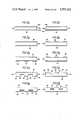
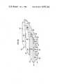
- FIG. 1is a partial perspective view of an electronic diode matrix array
- FIGS. 2A through 5Aare partial side views illustrating various stages of fabrication of the diode matrix array of FIG. 1;
- FIGS. 2B through 5Bare partial side views of the diode matrix array of FIG. 1 at the various stages of the fabrication thereof as viewed from a frame of reference perpendicular to the corresponding views of FIGS. 2A through 5A respectively;
- FIGS. 6A and 6Bare partial side views similar to FIGS. 5A and 5B respectively which illustrate an alternative method of isolating the diodes of the matrix ray;
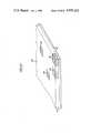
- FIG. 7is a partial perspective view of another electronic matrix array
- FIGS. 8A through 12Aare partial side views illustrating various states of fabrication of the electronic array of FIG. 7;
- FIGS. 8B through 12Bare partial side views of the electronic matrix array of FIG. 7 at the various states of the fabrication thereof as viewed from a frame of reference perpendicular to the corresponding views of FIGS. 8A through 12A respectively;
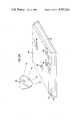
- FIG. 13is a partial perspective view of another electronic matrix array
- FIGS. 14A through 18Aare partial side views illustrating various stages of fabrication of the electronic array of FIG. 13;
- FIGS. 14B through 18Bare partial side views of the electronic matrix array of FIG. 13 at the various stages of the fabrication thereof as viewed from a frame of reference perpendicular to the corresponding views of FIGS. 14A. through 18A respectively;
- FIG. 19is a partial perspective view of a flat panel display
- FIG. 19Ais a schematic diagram of the equivalent circuit of the flat panel display of FIG. 19;
- FIG. 20is a partial perspective view of another flat panel display
- FIG. 20Ais a schematic diagram of the equivalent circuit of the flat panel display of FIG. 20.
- FIGS. 21 and 22are partial perspective views illustrating the method of making a preprogrammed array of circuits in accordance with one embodiment of the present invention
- FIG. 23is a partial perspective view of the preprogrammed array of circuits fabricated as shown in FIGS. 21 and 22;
- FIGS. 24 and 25are partial perspective views illustrating the method of making a preprogrammed electronic matrix memory array in accordance with another embodiment of the present invention.
- FIG. 26is a partial perspective view of the preprogrammed electronic matrix memory array fabricated as shown in FIGS. 24 and 25;
- FIG. 27is a partial perspective view of another electronic matrix memory array during fabrication in accordance with still another embodiment of the present invention.
- FIG. 28is a partial perspective view of the electronic matrix memory array partly fabricated in FIG. 25.
- FIGS. 1-20A and their descriptionsrefer to the electronic matrix arrays and method of making same in parent application Ser. No. 458,919, which is incorporated herein by reference.
- the structure and methods described thereinform an integral part of the array technology which is utilized in the parallel programming of the present invention, which is best described with regard to FIGS. 21-28.
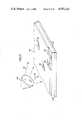
- the array 30generally includes a first plurality of conductive address lines 32, a second plurality of address lines 34, and a plurality of selection devices in the form of diodes 36 between the address lines 32 and 34.
- the first and second plurality of address linescross at an angle and are spaced apart by the diodes 36 to form a plurality of crossover points.
- the first and second address linesare orthogonally related and cross at an angle of 90°.
- the address linesare formed from parallel spaced apart bands of conductive material such as platinum or aluminum. Between each crossover point there is a diode 36.
- the diodesinclude a body of semiconductor material and preferably are formed from amorphous silicon alloys in accordance with the present invention. More particularly, and as will be further described with respect to FIGS. 2 through 5, the diodes preferably ar amorphous silicon alloys forming a p-i-n diode configuration.
- the selection devices or diodes 36are separated by orthogonally related grooves or channels 38.
- the grooves or channels 38are formed by etching the amorphous silicon alloys in the areas left exposed by address lines 32 and 34. This aids in providing electrical isolation between the diodes.
- the lateral conductivity of the amorphous silicon alloysare relatively low, such channels or grooves may not be necessary for all applications.
- the diodeshave an effective current conduction cross-sectional area formed by the overlapping juxtaposed common surface area of the address lines.
- FIGS. 2A through 5A, and 2B through 5Billustrate the fabrication process of the diode matrix array of FIG. 1.
- an amorphous silicon alloy p-i-n selection or diode structure 40is first formed on a conductive substrate 42.
- This continuous selection means structure 40preferably is a diode structure formed by a p-type amorphous silicon alloy region 40a, an intrinsic amorphous silicon alloy region 40b, and an n-type amorphous silicon alloy region 40 c.
- Amorphous silicon alloyscan be deposited in multiple layers over large area substrates to form such structures in high volume, continuous processing systems.
- Continuous processing systems of this kindare disclosed, for example, in pending patents: Ser. No. 151,301, filed May 19, 1980 for A Method Of Making P-Doped Silicon Films And Devices Made Therefrom, now U.S. Pat. No. 4,400,409 Ser. No. 244,386, filed Mar. 16, 1981 for Continuous Systems For Depositing Amorphous Semiconductor Material, now U.S. pat. No. 4,452,711 Ser. No. 240,493, filed Mar. 16, 1981 for Continuous Amorphous Solar Cell Production System, now U.S. Pat. No. 4,410,558; Ser. No. 306,146, filed Sept.
- a substrate formed from stainless steelmay be continuously advanced through a succession of deposition chambers, wherein each chamber is dedicated to the deposition of a specific material.
- a single deposition chamber systemcan be used for batch processing or preferably, a multiple chamber system can be used wherein a first chamber is used for depositing a p-type amorphous silicon alloy, a second chamber is used for depositing an intrinsic amorphous silicon alloy, and a third chamber is used for depositing an n-type amorphous silicon alloy. Since each deposited alloy, and specially the intrinsic alloy must be of high purity, the deposition environment in the intrinsic deposition chamber is preferably isolated from undesirable doping constituents within the other chambers to prevent the diffusion of doping constituents into the intrinsic chamber.
- isolation between the chambersis accomplished by gas gates through which unidirectional gas flow is established and through which an inert gas may be "swept" about the web of substrate material.
- deposition of the amorphous silicon alloy materials onto the large area continuous substrateis accomplished by glow discharge decomposition of the process gases.
- radio frequency energy glow discharge processeshave been found suitable for the continuous production of amorphous semiconductors, the first use of which has been as photovoltaic devices.
- a new and improved process for making amorphous semiconductor alloys and deviceshas recently been discovered. This process is disclosed in copending application Ser. No. 423,424, filed Sept. 24, 1982 for Method Of Making Amorphous Semiconductor Alloys and Devices Using Microwave Energy, now U.S. Pat. No. 4,517,223. This process utilizes microwave energy to decompose the reaction gases to cause the deposition of improved amorphous semiconductor materials.
- Microwave glow discharge processescan also be utilized in high volume mass production of devices as disclosed in copending application Ser. No. 441,280, filed Nov. 12, 1982, for An Improved Apparatus For The Manufacture Of Photovoltaic Devices, now U.S. Pat. No. 4,515,107, and to make layered structures as also disclosed in copending application Ser. No. 435,068, filed Oct. 18, 1982, for Method And Apparatus For Making Layered Amorphous Semiconductor Alloys Using Microwave Energy, now abandoned.
- the top layer of conductive material from which will be formed the first plurality of address lines 32is formed on the selection means or diode structure 40.
- the lines 32can be formed in parallel bands, for example, by conventional photo-lithography techniques of the type well known in the art.
- the second plurality of address lines 34are formed by removing selected portions of the substrate 42. This can be accomplished again, for example, by conventional photolithography techniques.
- FIGS. 4A and 4Brepresents a useful device in and of itself for many applications. This is due to the limited lateral conductivity of the amorphous silicon alloys comprising the diode structure.
- FIGS. 5A and 5B or FIGS. 6A and 6Bthe amorphous silicon diode structure 40 is etched to form the channels or grooves 38 in the areas thereof left exposed by the address lines 32 and 34.
- the address lines 32 and 34can be used as a mask during the etching operation.
- the amorphous silicon alloy diode structure 40need not be etched all the way through. In many cases, only the doped p and n-type regions need be etched through because these regions are of higher conductivity than the intrinsic region.
- a potting compoundcan be introduced into the grooves or channels 38 after the etching process. This can be done to provide increased structural integrity for the finished device.
- the diode structurecan be attached to another non-conductive substrae to provide increased structural integrity.
- the additional electrical isolation between the diodes 36can also be provided by oxidizing the amorphous silicon alloy diode structure in the selected areas left exposed by the address lines 32 and 34. This can be accomplished by using the address lines as a mask and by either implanting oxygen into the selected areas of the amorphous silicon alloys or by exposing the entire structure to a high temperature oxidizing atmosphere. The resulting device will then include oxidized regions 44 in the selected areas. Whether the etching or oxidizing process is employed to provide the additional electrical isolation between the diodes, the electrical conductivity of the diode structure in the selected areas will be modified by being decreased to thereby increase the electrical isolation between the diodes 36.
- the selection or diode structure 40can be formed from polycrystalline material. This can be accomplished by annealing the selection means structure 40 prior to forming the first plurality of address lines at a temperature which converts the amorphous silicon alloys to polycrystalline silicon alloys. For example, if the selection structure initially comprises amorphous silicon-hydrogen alloys, it can be annealed at 550° C.
- the photoconductive properties of the p-i-n diode structurescan be used to an advantage. Since the p-i-n diodes have photovoltaic characteristics, the diode matrix can be used as a data input terminal by, for example, shining light onto selected diodes. As a result, a detectable change in current will flow through selected respective pairs of the first and second address lines. This change in current, after detection, can be used for data input purposes.
- a transparent conductorsuch as indium tin oxide
- FIG. 7it illustrates another electronic matrix array 50 which can be ROM, PROM or EEPROM array, or, depending on intended use, a field programmable logic array.
- the electronic matrix array 50 of FIG. 7utilizes the diode matrix of FIG. 1 to facilitate individual selection or addressing of the memory cells of the devices.
- the elements which this array 50 have in common with the array 30 of FIG. 1have been assigned corresponding reference numerals.
- the arrayincludes a first plurality of address lines 32, a second plurality of address lines 34, and a plurality of selection devices or diodes 36 at each crossover point of the first and second address lines 32 and 34.
- the array 50includes a layer 52 of settable or resettable material between the diodes 36 and one of the plurality of address lines, here, the first plurality of address lines 32.
- the channels or grooves 38are provided to provide the previously mentioned additional electrical isolation.
- the arraywhen the layer 52 is formed from a settable material having a normal substantially non-conductive state and a settable substantially non-resettable comparatively high conductive state, the array can be either a ROM, PROM, or a field programmable logic array.
- the layer 52when the layer 52 is formed from a resettable material having a substantially non-conductive state and a comparatively high conductive state and which is settable and resettable between those states, the array comprises an EEPROM array.
- FIGS. 8 through 12illustrate a manner in which the array 50 of FIG. 7 can be fabricated.
- FIGS. 8A and 8Bshow that the diode structure 40 is first formed on the conductive substrate 42 as previously described. Then, the settable or resettable material 52 is deposited over the diode structure 40 as shown in FIGS. 9A and 9B. The first address lines 32 are then formed over the settable or resettable material 52 in a manner as previously described as shown in FIGS. 10A and 10B. Then, the second plurality of address lines are formed as previously described by etching portions of the substrate 42 as shown in FIGS. 11A and 11B. As before, the first and second plurality of address lines are formed so that they cross at an angle to form a plurality of crossover points.
- the areas of the amorphous silicon alloy and the resettable or resettable materialare etched using the address lines as a mask to form the channels or grooves 38 and the diode bodies 36 with the memory material 52 in series therewith.
- One preferred settable material from which the layer 52 can be formedis Si 50 C 50 .
- a memory cell made of this materialis substantially irreversible, i.e., substantially nonresettable.
- This cell materialhas a maximum processing temperature of up to 500° C. and a maximum storage temperature of from 200° C. up to approximately 400° C.
- Devices made from this materialcan have a threshold voltage of eight volts.
- the SET resistancecan be less than 500 ohms and an OFF resistance of up to 10 6 ohms.
- Silicon alloys produced by glow discharge or plasma deposition techniquehave properties and characteristics similar to those of the Si 50 C 50 material.
- One such materialis a silicon oxygen material wherein the silicon is 95 to 100 atomic percent and the oxygen is from 5 to 0 atomic percent with one preferred material being Si 95 O 5 .
- Other materials or alloyscan be formed from compound gases such as silane, silicon tetrafluoride, and hydrogen.
- the amorphous phase change materialsare deposited onto the diode structure 40 to the desired thickness.
- the deposition techniquescan be those described in the above referenced U.S. Pat. Nos. 4,217,374 and 4,226,898.
- One exemplary deposition processis a plasma deposition from SiH 4 which can include a diluent such as argon gas in about a one to one ratio.
- the substrate 42is heated to about or less than 150° centigrade.
- the materials or alloys described aboveprovide cell or memory region materials which have a stable, highly conductive state and a stable, highly non-conductive state.
- the non-conductive stateis substantially non-resettably switchable into the stable, highly conductive state by applying a current limited voltage pulse or a voltage limited current pulse across the cell region exceeding a predetermined threshold level.
- the cellremains in the highly conductive state even in the absence of an applied voltage or current and under all operating conditions.
- the memory materialcomprises a reversible, phase change material which can be set in a highly conductive state or a highly non-conductive state. More specifically, the layer 52 is formed of a material which is initially amorphous and which can be changed by a set voltage and current to a crystalline conductive state and then reset by a reset voltage and current to an amorphous insulator state or vice versa.
- One preferred material from which the resettable material can be madeincludes germanium and tellurium, such as Ge 20 Te 80 .
- This materialhas a good reversibility of up to 10 6 cycles, a maximum storage temperature of 100° C., a threshold voltage of 8 volts, a SET resistance of 300 ohms and OFF resistance (at 175° C.) of approximately 10 4 ohms.
- a thin barrier layer of molybdenumcan first be deposited by evaporation, for example, over the diode structure 40 to prevent migration.
- a ROM or PROM deviceresults.
- Selected individual memory cellscan be set by applying the required threshold voltage and current to selective respective pairs of the first and second address lines. Once set, a memory cell cannot be reset.
- a PROM arrayresults when the ultimate user does the programming, or a ROM array results if the array is programmed prior to receipt by the ultimate user.
- an EEPROM arrayresults. Such arrays, after once being programmed, can be reprogrammed.
- the array 50 of FIG. 7can also be used as a field programmable logic array.
- the array 50is used to that end when a settable material is used for layer 52.
- the diodesthemselves can be fused to form a bilaterally conducting via or open circuit as required.
- the diodescan be fused to form a conducting via for example by applying a large current to a selected pair of address lines to locally heat that diode to a temperature in excess of the crystallization temperature. This is electrically programming the conducting via.
- a selected diodecan be open circuited by passing an even larger current through the pair of address lines associated with that diode.
- This currentshould be sufficient to locally heat the amorphous silicon alloys forming the diode to a temperature which locally vaporizes the material to open circuit the same.
- field programmable logic arrayscan also be obtained in accordance with the present invention.
- laser energycan also be used to program the memory cell material.
- U.S. Pat. No. 3,530,441which issued to Stanford R. Ovshinsky on Sept. 22, 1970 discloses such a process and is incorporated herein by reference.
- laser energycan be used to short circuit or open circuit selected diodes when memory cell material is not employed. The laser beam however must be of sufficient energy and exposed to the selected diodes for a sufficient period of time to locally heat the diode semiconductor material to fuse or open circuit the same.
- One set of address linesmust therefore be transparent to laser light.
- FIG. 13it illustrates another electronic matrix array 60 which can be a ROM, PROM, or EEPROM array or a field programmable logic array depending on the memory material used and the manner of programming the memory cells and diodes.
- the array 60includes a first plurality of address lines 32, a second plurality of address lines 34, and a plurality of diodes 36 at the crossover points of the address lines 32 and 34.
- the array 60also includes a plurality of discrete layers 62 of settable or resettable material within the areas defined by the crossover points. Again, the discrete layers 62 can also be formed from transducer materials for the reasons previously mentioned.
- FIGS. 14 through 18A method of fabricating the array 60 is shown in FIGS. 14 through 18.
- the diode structure 40preferably of a p-i-n configuration, is formed on the substrate 42 in a manner as previously described.
- the memory materialis deposited in discrete layers 62 in those areas which will later be within the areas defined by the crossover points. This can be done, for example, by conventional masking and photolithography techniques.
- the first plurality of address lines 32is formed over the discrete layers of memory material 62 and diode structure 40.
- the second plurality of address lines 34is formed by etching, in selected areas, the substrate 42.
- a useful electronic matrix arraythen results.
- the areas of the amorphous silicon alloys left exposedcan either be etched as previously described or can be oxidized as previously described and as shown in FIGS. 18A and 18B. This leaves oxidized areas 64 to provide increased electrical isolation between the diodes 36.
- FIG. 19illustrates a horizontal liquid crystal cell structure 70 of that type. It is to be understood that FIG. 19 shows only one such cell and that many such cells can be made with it to form a flat panel display.
- the cell 70includes top conductors 72 and 74, bottom conductors 76, 78, and 80, a plurality of diode bodies 82, 84, 86, 88, 90, and 92, and a pair of display electrodes 94 and 96, electrode 94 being directly over diode bodies 86 and 88 and electrode 96 being formed over conductor 72.
- the top conductors 72 and 74are substantially parallel. They cross the bottom conductors 76, 78, and 80 and are spaced therefrom to form a plurality of crossover points. Within these crossover points and between the conductors are the diode bodies 82, 84, 90, and 92.
- the electrode 94also crosses conductors 78 and 80 to form a pair of crossover points wherein diode bodies 86 and 88 are located.
- the diodes 82, 90, and 92are open circuited and the diode body 88 is fused to a high conductivity state.
- Diodes 84 and 86have been left to function as diodes.
- a light influencing materialsuch as a liquid crystal material
- a light influencing materialis included between the electrodes 94 and 96.
- light influencing materialis meant any material which emits light or can be used to selectively vary the intensity, phase, or polarization of light either being reflected from or transmitted through the material. Liquid crystal material is only one such material having these characteristics.
- conductors 72 and 80are energized.
- conductors 72 and 74are energized.
- the structure of FIG. 19can be fabricated by starting with the selection means or diode structure deposited onto a conductive substrate as shown, for example, in FIGS. 14A and 14B. Thereafter, the top conductors and electrodes are deposited onto the diode structure in the configuration as shown. Thereafter, the substrate is etched to form the bottom conductors 76, 78, and 80. Then, the areas of amorphous silicon left exposed by the conductors and electrodes are etched using the conductors and electrodes as a mask. Diodes 82, 90, and 92 are then open circuited by passing a current therethrough sufficient to vaporize the material forming the diodes and diode body 88 is fused. Lastly, the liquid crystal material is introduced between the electrodes 94 and 96. A schematic diagram of the display cell 70 is shown in FIG. 19A.
- large area substrate and diode structurescan be employed as starting materials, large area flat panel displays can be made in accordance with the present invention. Also, because relatively few lithographic steps need be performed to make the device, small cell size and hence, increased packing density and resolution can be obtained.
- FIG. 20illustrates another flat panel display liquid crystal cell 100.
- This cellis a vertical cell and includes a relatively large area top electrode 102.
- the cell 100also includes top conductors 104 and 106 and bottom conductors 108, 110, and 112.
- Conductors 108 and 110cross under conductor 104 forming a pair of crossover points having therein diode bodies 116 and 118.
- Conductors 108 and 110also pass beneath electrode 102.
- the juxtaposed surface area of the conductors 108 and 112 with electrode 102contain therebetween diode bodies 124 and 126.
- conductors 112 and 108cross under conductor 106 forming another pair of crossover points having diode bodies 128 and 130 therein.
- diode bodies 120 and 122are between electrode 102 and conductor 112.
- Diode bodies 116 and 130have been open circuited
- diode bodies 118 and 128have been fused short circuited
- diode bodies 124, 126, 120, and 122remain functional as diodes.
- the transparent conductorwould be coupled to a source of common potential.
- Diodes 124 and 126form an AND gate. When the cell is energized a positive voltage is applied to conductors 104 and 108. To reset the cell, either one of conductors 104 and 108 is coupled to ground potential or a negative voltage.
- the cell 100can be fabricated by starting with the deposited diode structure over a conductive substrate as shown, for example, in FIGS. 14A and 14B. Then, the top conductors 104 and 106 and the electrode 102 are deposited on top of the diode structure in the desired configuration as shown. Then, the substrate is etched to form the bottom conductors 108, 110, and 112. Then, the areas of the amorphous silicon diode structure left exposed by the conductors and electrodes are etched to form the diode bodies. Thereafter, diodes 116 and 130 are open circuited by passing a current through the diodes sufficient to vaporize localized regions of the amorphous silicon forming the diodes to open circuit the same.
- Diode bodies 110 and 128are short circuited by passing a current therethrough sufficient to heat the amorphous silicon alloys forming the diode bodies to a temperature which crystallizes the material.
- the liquid crystal materialis applied over the electrode 102 and the common electrode is applied over the liquid crystal material.
- the open spaces beneath the cellcan be potted with a potting compound to increase the physical integrity of the cell if desired.
- FIGS. 21 and 22they illustrate a preprogrammed electronic array of circuits 140 as shown in FIG. 23 at intermediate stages of fabrication in accordance with the present invention.
- the matrix array fabricationbegins with a conductive substrate 142.
- Formed on the substrate 142is at least one layer 144 of phase changeable material which can be either settable or resettable material and includes the diode structure, as previously described.
- the layer 144is a diode structure formed from amorphous silicon alloys.
- the diode structurecan have p-i-n configuration and be formed by depositing a p-type layer onto substrate 142, an intrinsic layer over the p-type layer, and then an n-type layer over the instrinsic layer. Such a procedure has been previously described and can be used to form the diode structure.
- a mask 146is applied to the diode structure 144.
- the maskincludes one or more openings 148 configured to define and expose selected portions of the diode structure 144 to be irradiated for changing the selected portions from the substantially nonconductive state of the amorphous silicon to the comparatively high conductive state of crystalline material.
- the openings 148are also preferably configured to define areas substantially the same as the cross sectional area of the crossover points formed by the overlapping juxtaposed common surface area of the address lines to be subsequently formed.
- the mask 146can be a physically separate sheet of material brought into contact with the diode structure 144 or can be a photoresist formed over the diode structure with the openings 148 being formed by conventional photolithography techniques.
- a high-intensity photoflash lamp 149is provided.
- a xenon photoflash lampis a particularly useful and effective photoflash lamp for this application. It directs a wide angle light beam 150 to impinge upon the entire area of the mask 146.
- the selected areas of the diode structureare flashed or irradiated by the lamp 149 through the mask, the selected areas will be locally heated for changing the state of the material in the substrate areas from the substantially nonconductive state to the comparatively high conductive state.
- the maskis then removed by physically removing the same if it is a physically integral sheet of material, or by chemical treatment if it is formed of a photoresist material.
- the partially completed matrix arraywill then appear as illustrated in FIG. 22.
- FIG. 23it illustrates a completed electronic matrix array 140 which has been fabricated in accordance with this embodiment of the present invention. While the array 140 is not a memory array, it can be extremely useful to establish selected circuits for use in logic arrays and flat panel displays, for example.
- a first set of address lines 156have been formed by removing portions of the conductive substrate 142.
- a second set of address lines 158have also been formed over the diode structure.
- the address lines 158can be formed by conventional evaporation processes as previously disclosed and configured by conventional photolithography procedures.
- the address lines 158can also be aligned with the phase changed areas 152 by detecting the location of the areas 152.
- phase changed selected areas 152will have optical properties different from the other areas 154 which were not changed in phase. Thereafter, the address lines 158 can be aligned in accordance with the detected locations of the selected areas 152.
- the first and second sets of address lines 156 and 158cross at an angle to form crossover points.
- the juxtaposed common surface area of the address linestherefore define diode bodies 160 in those areas which were not phase changed.
- the selected areas 152 which were phase changedwill function as shorted diodes.
- the electronic matrix array 140will function like the electronic matrix array 30 of FIG. 1, but will be preprogrammed.
- the address lines 156 and 158can be applied using the same lamp 149 and lens system (not illustrated) as utilized to program the array. Therefore, any optical misalignment or optical curvature will be aligned in each layer and the crossover points will retain their alignment even though the lines may not be perfectly straight and perpendicular to one another.
- the array 140can be manufactured to be field programmable in a substantially similar fashion to that described above, the difference being that the layer 144 is not preprogrammed during manufacture.
- the structureis completed as shown in FIG. 23 and then can be field programmed by utilizing a mask similar to the mask 146.
- at least one set of the address lines 156 or 158is transparent to the programming light so that the selected diodes 152 can be switched through the lines.
- the areas of the diode structure left exposed by the address lines 156 and 158have been partially removed by utilizing the address lines as a mask. This alters the conductivity or resistivity between the diode bodies 160 and the selected diode structure portions 152 or between the diode bodies 160 before field programming for increasing the isolation therebetween. As previously mentioned, this may not be necessary for many applications.
- FIGS. 24 and 25they illustrate a preprogrammed electronic matrix array 170 as shown in FIG. 26 at intermediate stages of fabrication in accordance with another embodiment of the present invention.
- the array 170can be used as a PROM, a ROM, or an EEPROM, depending on the materials used for forming the phase changeable layer as will be described hereinafter.
- the matrix array fabricationbegins with a conductive substrate 172. Formed on the substrate 172 is a continuous selection means or diode structure 174 of the type previously referred to. Deposited or formed over the diode structure 174 is a layer of phase changeable material 176.
- the phase changeable material forming layer 176is preferably settable or resettable material as previously described.
- the layer 176is formed from settable material which has a substantially nonconductive state and a settable, substantially nonresettable, comparatively high conductive state.
- a materialcan be, for example, an amorphous silicon alloy as previously described, or a doped amorphous silicon alloy as disclosed in copending application Ser. No. 281,018, filed July 6, 1981, for An Improved Programmable Cell For Use In Programmable Electronic Arrays, now U.S. Pat. No. 4,499,557 which is assigned to the assignee of the present invention.
- the layeris formed from a resettable material which has a substantially nonconductive state and a comparatively high conductive state and which can be set and reset between these two states.
- a resettable materialcan be, for example, a chalcogenide as previously described.
- a mask 178is placed or formed over the layer 176.
- the maskcan take the form of mask 146 of FIG. 21.
- the mask 178also has openings 180 configured to define and expose selected portions of the layer 176 to be irradiated for changing the selected portions from the substantially nonconductive state to the comparatively high conductive state.
- the openings 180are also preferably configured to define areas of substantially the same cross sectional area at the crossover points formed by the overlapping juxtaposed common surface area of the address lines to be subsequently formed.
- a high-intensity photoflash lamp 182is provided. It can be of the type as previously referred to with respect to lamp 149 of FIG. 21. Once the selected areas of the layer 176 are flashed or irradiated by the lamp 182, the selected areas will have been locally changed from the substantially nonconductive state to the comparatively high conductive state. Here, the energy supplied to the lamp must be controlled so that only the layer 176 in the selected areas change state, and not the diode structure 174 beneath the layer 176.
- the mask 178is removed by physically removing the same if it is a physically integral sheet of material, or by chemical or other removal treatment if it is formed of a photoresist material.
- the partially completed matrix arraywill then appear as illustrated in FIG. 25.
- FIG. 25it can be seen that the selected areas 184 which were exposed to the light radiation have been changed to the comparatively high conductive state.
- the remaining portions 186 of the layer 176are left in the substantially nonconductive state because these areas were not exposed to the light radiation.
- FIG. 26it illustrates a completed electronic matrix array 170 which has been fabricated in accordance with this embodiment of the present invention.
- a first set of address lines 188have been formed by removing portions of the conductive substrate 172.
- a second set of address lines 190have also been formed over the diode structure.
- the address lines 190can be formed by conventional evaporation processes as previously disclosed and configured by conventional photolithograph procedures.
- the address lines 190can also be aligned with the phase changed areas 184 by detecting the location of the areas 184. This can be done, for example, by optical techniques known in the art because the phase changed selected areas 184 will have optical properties different from the other areas 186 which were not changed in phase. Thereafter, the address lines 190 can be aligned in accordance with the detected locations of the selected areas 184.
- the first and second sets of address lines 188 and 190cross at an angle to form crossover points.
- the juxtaposed common surface area of the address linestherefore define diode bodies 192 in series with the programmed layer portions 184 and 186.
- the electronic matrix array 170will function like the electronic matrix array 50 of FIG. 7, but will be preprogrammed.
- the selected switched crossover points 184also can be tested after programming to ensure that the correct information is encoded in the array 170.
- the areas 184 and remaining areascan be read or sensed by optical means, such as a laser as previously described.
- the information or pattern encodedcan be read optically or electrically.
- the areas which are not properly programmedcan be individually programmed by optical means, in the case of the preprogrammed array, or optical or electrical means, in the case of the field programmable array.
- the arraymay be cooled before and/or during programming. This avoids unwanted heat transfer to other parts of a device in which the array 170 is incorporated. Cooling also can facilitate individual area switching after testing to avoid heating adjacent areas.
- the array 170can also be formed in a field programmable embodiment by not preprogramming the areas 184. Again, one set of lines 188 or 190 must be transparent to the programming light, the array 170 can be cooled during programming and the programmed array 170 can be tested and reprogrammed if necessary. If the layer 176 is formed of resettable material, then the array 170 can also be bulk erased and reprogrammed.
- the areas of the diode structure and the layer of settable or resettable material left exposed by the address lines 188 and 190have been partially removed by utilizing the address lines as a mask. This alters the conductivity or resistivity between the diode bodies 192 for increasing the isolation therebetween. As previously mentioned, this may not be necessary for many applications.
- the selected areas 184were converted to the comparatively high conductive state. In doing so, those areas 184 were changed from the amorphous phase to crystalline phase.
- the difference in structure between the areas 184 and the areas 186can be used to advantage in making a preprogrammed electronic array wherein the selected portions of the array rendered highly conductive cannot be reset to a substantially nonconductive state.
- the layer 176can be subjected to a wet etchant such as nitric acid, which will selectively etch the crystalline phase portions 184 at a faster rate than the amorphous portions 186.
- a wet etchantsuch as nitric acid
- FIG. 25the structure of FIG. 25 will take the form as shown in FIG. 27.
- the crystalline phase portions 184have been removed forming voids 200 with the diode structure 174 exposed therebeneath and that the amorphous or substantially nonconductive portion 186 remains on top of the diode structure 174.
- the second set of address lines 190will directly contact the diode structure in those areas which were exposed to the light radiation and removed by the etchant.
- diode bodies 192a and 192bare in direct contact with the address line 190 which overlies them.
- the array of FIG. 28is substantially identical to the array 170 of FIG. 26.
- the amorphous silicon diode bodiescan have numerous sizes and shapes and can also have an n-i-p configuration.
- multiple p-i-n structurescan be deposited in tandem to form multiple diode structures.
- a multi-level structureis formed with many levels of electrically interconnectable programmable diode cells. Multiple diode structures would be desired for some operating voltage and current requirements and multi-level structures are desired for maximum gate or bit density and minimum interconnecting circuit lengths.
- the resettable materialscan also be initially formed in the crystalline state prior to being irradiated.
- amorphousis meant an alloy or material which has long range disorder, although it can have short or intermediate order or even contain at times crystalline inclusions.
- a suitable etchantcan be selected to remove the amorphous areas instead of the crystalline areas if so desired.
- the arraycan include alignment areas which are preprogrammed to facilitate the field programming alignment. It is therefore, to be understood that within the scope of the appended claims the invention can be practiced otherwise than as specifically described.
Landscapes
- Semiconductor Memories (AREA)
- Design And Manufacture Of Integrated Circuits (AREA)
- Solid State Image Pick-Up Elements (AREA)
- Logic Circuits (AREA)
- Read Only Memory (AREA)
- Electrochromic Elements, Electrophoresis, Or Variable Reflection Or Absorption Elements (AREA)
- Semiconductor Integrated Circuits (AREA)
Abstract
Description
______________________________________ U.S. Pat. No. PATENTEE ______________________________________ 3,571,809 Nelson 3,573,757 Adams 3,629,863 Neale 3,699,543 Neale 3,846,767 Cohen 3,886,577 Buckley 3,875,566 Helbers 3,877,049 Buckley 3,922,648 Buckely 3,980,505 Buckley 4,177,475 Holmberg ______________________________________
Claims (28)
Priority Applications (1)
| Application Number | Priority Date | Filing Date | Title |
|---|---|---|---|
| US06/785,367US4597162A (en) | 1983-01-18 | 1985-10-07 | Method for making, parallel preprogramming or field programming of electronic matrix arrays |
Applications Claiming Priority (3)
| Application Number | Priority Date | Filing Date | Title |
|---|---|---|---|
| US45891983A | 1983-01-18 | 1983-01-18 | |
| US06/513,997US4545111A (en) | 1983-01-18 | 1983-07-14 | Method for making, parallel preprogramming or field programming of electronic matrix arrays |
| US06/785,367US4597162A (en) | 1983-01-18 | 1985-10-07 | Method for making, parallel preprogramming or field programming of electronic matrix arrays |
Related Parent Applications (1)
| Application Number | Title | Priority Date | Filing Date |
|---|---|---|---|
| US06/513,997ContinuationUS4545111A (en) | 1983-01-18 | 1983-07-14 | Method for making, parallel preprogramming or field programming of electronic matrix arrays |
Publications (1)
| Publication Number | Publication Date |
|---|---|
| US4597162Atrue US4597162A (en) | 1986-07-01 |
Family
ID=27039156
Family Applications (2)
| Application Number | Title | Priority Date | Filing Date |
|---|---|---|---|
| US06/513,997Expired - LifetimeUS4545111A (en) | 1983-01-18 | 1983-07-14 | Method for making, parallel preprogramming or field programming of electronic matrix arrays |
| US06/785,367Expired - LifetimeUS4597162A (en) | 1983-01-18 | 1985-10-07 | Method for making, parallel preprogramming or field programming of electronic matrix arrays |
Family Applications Before (1)
| Application Number | Title | Priority Date | Filing Date |
|---|---|---|---|
| US06/513,997Expired - LifetimeUS4545111A (en) | 1983-01-18 | 1983-07-14 | Method for making, parallel preprogramming or field programming of electronic matrix arrays |
Country Status (10)
| Country | Link |
|---|---|
| US (2) | US4545111A (en) |
| EP (1) | EP0117046B1 (en) |
| KR (1) | KR930000719B1 (en) |
| AT (1) | ATE44335T1 (en) |
| AU (1) | AU561855B2 (en) |
| BR (1) | BR8400201A (en) |
| CA (1) | CA1212470A (en) |
| DE (1) | DE3478836D1 (en) |
| IL (1) | IL70716A (en) |
| IN (1) | IN160151B (en) |
Cited By (109)
| Publication number | Priority date | Publication date | Assignee | Title |
|---|---|---|---|---|
| US4783424A (en)* | 1981-09-03 | 1988-11-08 | Tokyo Shibaura Denki Kabushiki Kaisha | Method of making a semiconductor device involving simultaneous connection and disconnection |
| US4818717A (en)* | 1986-06-27 | 1989-04-04 | Energy Conversion Devices, Inc. | Method for making electronic matrix arrays |
| US4842372A (en)* | 1986-10-22 | 1989-06-27 | Seiko Instruments Inc. | Electro-optical device having an amorphous silicon resistive element with carbon |
| US4868616A (en)* | 1986-12-11 | 1989-09-19 | Energy Conversion Devices, Inc. | Amorphous electronic matrix array for liquid crystal display |
| US4871234A (en)* | 1985-05-15 | 1989-10-03 | Seiko Instruments Inc. | Liquid crystal display device |
| US4900691A (en)* | 1987-04-17 | 1990-02-13 | Kanegafuchi Chemical Industry Company, Limited | Method of fabrication for optical storage apparatus |
| US4904057A (en)* | 1986-12-06 | 1990-02-27 | Semiconductor Energy Laboratory Co., Ltd. | Liquid crystal device with a smectic chiral liquid crystal and with a rectifier in series with each pixel |
| US4925276A (en)* | 1987-05-01 | 1990-05-15 | Electrohome Limited | Liquid crystal light valve utilizing hydrogenated amorphous silicon photodiode |
| US4969021A (en)* | 1989-06-12 | 1990-11-06 | California Institute Of Technology | Porous floating gate vertical mosfet device with programmable analog memory |
| US5042917A (en)* | 1986-04-25 | 1991-08-27 | Matsushita Electric Industrial Co., Ltd. | Liquid crystal matrix display unit |
| US5061040A (en)* | 1984-01-23 | 1991-10-29 | Ois Optical Imaging Systems, Inc. | Liquid crystal displays operated by amorphous silicon alloy diodes |
| US5367208A (en)* | 1986-09-19 | 1994-11-22 | Actel Corporation | Reconfigurable programmable interconnect architecture |
| US5527745A (en)* | 1991-03-20 | 1996-06-18 | Crosspoint Solutions, Inc. | Method of fabricating antifuses in an integrated circuit device and resulting structure |
| US5741720A (en)* | 1995-10-04 | 1998-04-21 | Actel Corporation | Method of programming an improved metal-to-metal via-type antifuse |
| US5751012A (en)* | 1995-06-07 | 1998-05-12 | Micron Technology, Inc. | Polysilicon pillar diode for use in a non-volatile memory cell |
| US6190986B1 (en)* | 1999-01-04 | 2001-02-20 | International Business Machines Corporation | Method of producing sulithographic fuses using a phase shift mask |
| US6291836B1 (en)* | 1996-06-05 | 2001-09-18 | U. S. Philips Corporation | Method of operating a programmable, non-volatile memory device |
| US20020168852A1 (en)* | 2001-05-11 | 2002-11-14 | Harshfield Steven T. | PCRAM memory cell and method of making same |
| US20030022420A1 (en)* | 2000-04-28 | 2003-01-30 | Bendik Kleveland | Three-dimensional memory array incorporating serial chain diode stack |
| US20030027416A1 (en)* | 2001-08-01 | 2003-02-06 | Moore John T. | Method of forming integrated circuitry, method of forming memory circuitry, and method of forming random access memory circuitry |
| US20030045049A1 (en)* | 2001-08-29 | 2003-03-06 | Campbell Kristy A. | Method of forming chalcogenide comprising devices |
| US6535418B2 (en)* | 2001-07-24 | 2003-03-18 | Hewlett-Packard Development Company, Llp | Optically programmable address logic for solid state diode-based memory |
| US20030096497A1 (en)* | 2001-11-19 | 2003-05-22 | Micron Technology, Inc. | Electrode structure for use in an integrated circuit |
| US20030117831A1 (en)* | 2001-12-20 | 2003-06-26 | Glen Hush | Programmable conductor random access memory and a method for writing thereto |
| US20030128612A1 (en)* | 2002-01-04 | 2003-07-10 | John Moore | PCRAM rewrite prevention |
| US20030156468A1 (en)* | 2002-02-20 | 2003-08-21 | Campbell Kristy A. | Resistance variable 'on' memory |
| US20030194865A1 (en)* | 2002-04-10 | 2003-10-16 | Gilton Terry L. | Method of manufacture of programmable conductor memory |
| US6642102B2 (en)* | 2001-06-30 | 2003-11-04 | Intel Corporation | Barrier material encapsulation of programmable material |
| EP1367596A1 (en)* | 2002-05-31 | 2003-12-03 | Hewlett-Packard Company | Cross-point diode ROM |
| US20040007749A1 (en)* | 2002-07-10 | 2004-01-15 | Campbell Kristy A. | Assemblies displaying differential negative resistance |
| US20040007718A1 (en)* | 2001-08-30 | 2004-01-15 | Campbell Kristy A. | Stoichiometry for chalcogenide glasses useful for memory devices and method of formation |
| US20040029351A1 (en)* | 2002-01-31 | 2004-02-12 | Gilton Terry L. | Methods of forming non-volatile resistance variable devices and methods of forming silver selenide comprising structures |
| US20040040837A1 (en)* | 2002-08-29 | 2004-03-04 | Mcteer Allen | Method of forming chalcogenide sputter target |
| US20040043245A1 (en)* | 2002-08-29 | 2004-03-04 | Moore John T. | Method to control silver concentration in a resistance variable memory element |
| US20040053461A1 (en)* | 2002-08-29 | 2004-03-18 | Moore John T. | Graded GexSe100-x concentration in PCRAM |
| US20040130598A1 (en)* | 2002-07-10 | 2004-07-08 | Canon Kabushiki Kaisha | Ink jet record head |
| US20040161874A1 (en)* | 2001-03-01 | 2004-08-19 | Moore John T. | Method of forming a non-volatile resistance variable device, and non-volatile resistance variable device |
| US20040175859A1 (en)* | 2002-08-29 | 2004-09-09 | Campbell Kristy A. | Single polarity programming of a PCRAM structure |
| US6791885B2 (en) | 2002-02-19 | 2004-09-14 | Micron Technology, Inc. | Programmable conductor random access memory and method for sensing same |
| US20040202016A1 (en)* | 2003-04-10 | 2004-10-14 | Campbell Kristy A. | Differential negative resistance memory |
| US6809362B2 (en) | 2002-02-20 | 2004-10-26 | Micron Technology, Inc. | Multiple data state memory cell |
| US20040211957A1 (en)* | 2002-08-29 | 2004-10-28 | Moore John T. | Method and apparatus for controlling metal doping of a chalcogenide memory element |
| US6813178B2 (en) | 2003-03-12 | 2004-11-02 | Micron Technology, Inc. | Chalcogenide glass constant current device, and its method of fabrication and operation |
| US6825135B2 (en) | 2002-06-06 | 2004-11-30 | Micron Technology, Inc. | Elimination of dendrite formation during metal/chalcogenide glass deposition |
| US6833559B2 (en) | 2001-02-08 | 2004-12-21 | Micron Technology, Inc. | Non-volatile resistance variable device |
| US20040264234A1 (en)* | 2003-06-25 | 2004-12-30 | Moore John T. | PCRAM cell operation method to control on/off resistance variation |
| US6849868B2 (en) | 2002-03-14 | 2005-02-01 | Micron Technology, Inc. | Methods and apparatus for resistance variable material cells |
| US6855975B2 (en) | 2002-04-10 | 2005-02-15 | Micron Technology, Inc. | Thin film diode integrated with chalcogenide memory cell |
| US6864500B2 (en) | 2002-04-10 | 2005-03-08 | Micron Technology, Inc. | Programmable conductor memory cell structure |
| US6867114B2 (en) | 2002-08-29 | 2005-03-15 | Micron Technology Inc. | Methods to form a memory cell with metal-rich metal chalcogenide |
| US6867064B2 (en) | 2002-02-15 | 2005-03-15 | Micron Technology, Inc. | Method to alter chalcogenide glass for improved switching characteristics |
| US6878569B2 (en) | 2001-03-15 | 2005-04-12 | Micron Technology, Inc. | Agglomeration elimination for metal sputter deposition of chalcogenides |
| US6890790B2 (en) | 2002-06-06 | 2005-05-10 | Micron Technology, Inc. | Co-sputter deposition of metal-doped chalcogenides |
| US6894304B2 (en) | 2001-08-27 | 2005-05-17 | Micron Technology, Inc. | Apparatus and method for dual cell common electrode PCRAM memory device |
| US6903361B2 (en) | 2003-09-17 | 2005-06-07 | Micron Technology, Inc. | Non-volatile memory structure |
| US20050162907A1 (en)* | 2004-01-28 | 2005-07-28 | Campbell Kristy A. | Resistance variable memory elements based on polarized silver-selenide network growth |
| US20050167689A1 (en)* | 2004-01-29 | 2005-08-04 | Campbell Kristy A. | Non-volatile zero field splitting resonance memory |
| US6937528B2 (en) | 2002-03-05 | 2005-08-30 | Micron Technology, Inc. | Variable resistance memory and method for sensing same |
| US6961277B2 (en) | 2003-07-08 | 2005-11-01 | Micron Technology, Inc. | Method of refreshing a PCRAM memory device |
| US20050242338A1 (en)* | 2004-04-30 | 2005-11-03 | Hart Mark W | Non-planarized, self-aligned, non-volatile phase-change memory array and method of formation |
| US6998697B2 (en) | 2001-08-29 | 2006-02-14 | Micron Technology, Inc. | Non-volatile resistance variable devices |
| US7002833B2 (en) | 2001-11-20 | 2006-02-21 | Micron Technology, Inc. | Complementary bit resistance memory sensor and method of operation |
| US7010644B2 (en) | 2002-08-29 | 2006-03-07 | Micron Technology, Inc. | Software refreshed memory device and method |
| US7018863B2 (en) | 2002-08-22 | 2006-03-28 | Micron Technology, Inc. | Method of manufacture of a resistance variable memory cell |
| US7022579B2 (en) | 2003-03-14 | 2006-04-04 | Micron Technology, Inc. | Method for filling via with metal |
| US20060071272A1 (en)* | 2004-10-01 | 2006-04-06 | International Business Machines Corporation | Programmable non-volatile resistance switching device |
| US7049009B2 (en) | 2002-08-29 | 2006-05-23 | Micron Technology, Inc. | Silver selenide film stoichiometry and morphology control in sputter deposition |
| US7061004B2 (en) | 2003-07-21 | 2006-06-13 | Micron Technology, Inc. | Resistance variable memory elements and methods of formation |
| US7087919B2 (en) | 2002-02-20 | 2006-08-08 | Micron Technology, Inc. | Layered resistance variable memory device and method of fabrication |
| US7094700B2 (en) | 2002-08-29 | 2006-08-22 | Micron Technology, Inc. | Plasma etching methods and methods of forming memory devices comprising a chalcogenide comprising layer received operably proximate conductive electrodes |
| US7098068B2 (en) | 2004-03-10 | 2006-08-29 | Micron Technology, Inc. | Method of forming a chalcogenide material containing device |
| US20060268603A1 (en)* | 2002-01-09 | 2006-11-30 | Peter Nangle | Programming method for non-volatile memory |
| US7151688B2 (en) | 2004-09-01 | 2006-12-19 | Micron Technology, Inc. | Sensing of resistance variable memory devices |
| US7177183B2 (en) | 2003-09-30 | 2007-02-13 | Sandisk 3D Llc | Multiple twin cell non-volatile memory array and logic block structure and method therefor |
| US7190048B2 (en) | 2004-07-19 | 2007-03-13 | Micron Technology, Inc. | Resistance variable memory device and method of fabrication |
| US7209378B2 (en) | 2002-08-08 | 2007-04-24 | Micron Technology, Inc. | Columnar 1T-N memory cell structure |
| US20070133248A1 (en)* | 2005-12-08 | 2007-06-14 | Macronix International Co., Ltd. | Diode-less array for one-time programmable memory |
| US7233520B2 (en) | 2005-07-08 | 2007-06-19 | Micron Technology, Inc. | Process for erasing chalcogenide variable resistance memory bits |
| US7251154B2 (en) | 2005-08-15 | 2007-07-31 | Micron Technology, Inc. | Method and apparatus providing a cross-point memory array using a variable resistance memory cell and capacitance |
| US7269044B2 (en) | 2005-04-22 | 2007-09-11 | Micron Technology, Inc. | Method and apparatus for accessing a memory array |
| US7269079B2 (en) | 2005-05-16 | 2007-09-11 | Micron Technology, Inc. | Power circuits for reducing a number of power supply voltage taps required for sensing a resistive memory |
| US7274034B2 (en) | 2005-08-01 | 2007-09-25 | Micron Technology, Inc. | Resistance variable memory device with sputtered metal-chalcogenide region and method of fabrication |
| US7277313B2 (en) | 2005-08-31 | 2007-10-02 | Micron Technology, Inc. | Resistance variable memory element with threshold device and method of forming the same |
| US20070231972A1 (en)* | 2006-04-03 | 2007-10-04 | Mouttet Blaise L | Manufacture of programmable crossbar signal processor |
| US20070229111A1 (en)* | 2006-04-03 | 2007-10-04 | Blaise Laurent Mouttet | Programmable crossbar signal processor with rectification layer |
| US7294527B2 (en) | 2002-08-29 | 2007-11-13 | Micron Technology Inc. | Method of forming a memory cell |
| US7304368B2 (en) | 2005-08-11 | 2007-12-04 | Micron Technology, Inc. | Chalcogenide-based electrokinetic memory element and method of forming the same |
| US7317200B2 (en) | 2005-02-23 | 2008-01-08 | Micron Technology, Inc. | SnSe-based limited reprogrammable cell |
| US7317567B2 (en) | 2005-08-02 | 2008-01-08 | Micron Technology, Inc. | Method and apparatus for providing color changing thin film material |
| US7326950B2 (en) | 2004-07-19 | 2008-02-05 | Micron Technology, Inc. | Memory device with switching glass layer |
| US7332735B2 (en) | 2005-08-02 | 2008-02-19 | Micron Technology, Inc. | Phase change memory cell and method of formation |
| US7354793B2 (en) | 2004-08-12 | 2008-04-08 | Micron Technology, Inc. | Method of forming a PCRAM device incorporating a resistance-variable chalocogenide element |
| US20080093589A1 (en)* | 2004-12-22 | 2008-04-24 | Micron Technology, Inc. | Resistance variable devices with controllable channels |
| US7365411B2 (en) | 2004-08-12 | 2008-04-29 | Micron Technology, Inc. | Resistance variable memory with temperature tolerant materials |
| US7374174B2 (en) | 2004-12-22 | 2008-05-20 | Micron Technology, Inc. | Small electrode for resistance variable devices |
| US7396699B2 (en) | 2001-08-29 | 2008-07-08 | Micron Technology, Inc. | Method of forming non-volatile resistance variable devices and method of forming a programmable memory cell of memory circuitry |
| US20080212382A1 (en)* | 2006-04-03 | 2008-09-04 | Blaise Laurent Mouttet | Crossbar waveform driver circuit |
| US7427770B2 (en) | 2005-04-22 | 2008-09-23 | Micron Technology, Inc. | Memory array for increased bit density |
| US20080246116A1 (en)* | 2006-04-03 | 2008-10-09 | Blaise Laurent Mouttet | Symmetrical programmable crossbar structure |
| US20080307151A1 (en)* | 2006-04-03 | 2008-12-11 | Blaise Laurent Mouttet | Operational amplifier with resistance switch crossbar feedback |
| US7579615B2 (en) | 2005-08-09 | 2009-08-25 | Micron Technology, Inc. | Access transistor for memory device |
| US7583551B2 (en) | 2004-03-10 | 2009-09-01 | Micron Technology, Inc. | Power management control and controlling memory refresh operations |
| US7663133B2 (en) | 2005-04-22 | 2010-02-16 | Micron Technology, Inc. | Memory elements having patterned electrodes and method of forming the same |
| US7723713B2 (en) | 2002-02-20 | 2010-05-25 | Micron Technology, Inc. | Layered resistance variable memory device and method of fabrication |
| US20100182044A1 (en)* | 2007-03-13 | 2010-07-22 | Easic Corporation | Programming and circuit topologies for programmable vias |
| US7791058B2 (en) | 2006-08-29 | 2010-09-07 | Micron Technology, Inc. | Enhanced memory density resistance variable memory cells, arrays, devices and systems including the same, and methods of fabrication |
| US8467236B2 (en) | 2008-08-01 | 2013-06-18 | Boise State University | Continuously variable resistor |
| WO2016007035A1 (en)* | 2014-07-07 | 2016-01-14 | Nokia Technologies Oy | Sensing device and method of production thereof |
| US20170338282A1 (en)* | 2016-05-20 | 2017-11-23 | Intel Corporation | Memory module with unpatterned storage material |
Families Citing this family (30)
| Publication number | Priority date | Publication date | Assignee | Title |
|---|---|---|---|---|
| US4677742A (en)* | 1983-01-18 | 1987-07-07 | Energy Conversion Devices, Inc. | Electronic matrix arrays and method for making the same |
| US4545111A (en)* | 1983-01-18 | 1985-10-08 | Energy Conversion Devices, Inc. | Method for making, parallel preprogramming or field programming of electronic matrix arrays |
| GB8333033D0 (en)* | 1983-12-10 | 1984-01-18 | British Petroleum Co Plc | Memory device |
| US4665295A (en)* | 1984-08-02 | 1987-05-12 | Texas Instruments Incorporated | Laser make-link programming of semiconductor devices |
| JPS6188578A (en)* | 1984-10-08 | 1986-05-06 | Nec Corp | nonlinear element |
| US4679085A (en)* | 1984-12-04 | 1987-07-07 | Energy Conversion Devices, Inc. | Digital integrated electronic storage system for video and audio playback |
| JPS61198779A (en)* | 1985-02-28 | 1986-09-03 | Res Dev Corp Of Japan | Electrostatic induction thyristor having gates on both surfaces and manufacture thereof |
| US4715685A (en)* | 1985-03-04 | 1987-12-29 | Energy Conversion Devices, Inc. | Liquid crystal display having potential source in a diode ring |
| US4630355A (en)* | 1985-03-08 | 1986-12-23 | Energy Conversion Devices, Inc. | Electric circuits having repairable circuit lines and method of making the same |
| FR2579806B1 (en)* | 1985-03-26 | 1987-05-07 | Morin Francois | METHOD FOR MANUFACTURING A LIQUID CRYSTAL AND DIODE ARRAY DISPLAY SCREEN |
| US4906987A (en)* | 1985-10-29 | 1990-03-06 | Ohio Associated Enterprises, Inc. | Printed circuit board system and method |
| US4789883A (en)* | 1985-12-17 | 1988-12-06 | Advanced Micro Devices, Inc. | Integrated circuit structure having gate electrode and underlying oxide and method of making same |
| DE3602796A1 (en)* | 1986-01-30 | 1987-08-06 | Messerschmitt Boelkow Blohm | SENSOR ELEMENT WITH A MEMORY FOR ABNORMAL CHANGES IN THE INCIDENT LIGHT INTENSITY |
| US4782340A (en)* | 1986-08-22 | 1988-11-01 | Energy Conversion Devices, Inc. | Electronic arrays having thin film line drivers |
| US5188974A (en)* | 1987-10-31 | 1993-02-23 | Canon Kabushiki Kaisha | Method of manufacturing semiconductor device |
| US5989943A (en)* | 1989-09-07 | 1999-11-23 | Quicklogic Corporation | Method for fabrication of programmable interconnect structure |
| US5502315A (en)* | 1989-09-07 | 1996-03-26 | Quicklogic Corporation | Electrically programmable interconnect structure having a PECVD amorphous silicon element |
| US6159753A (en)* | 1996-12-20 | 2000-12-12 | Intel Corporation | Method and apparatus for editing an integrated circuit |
| US5837564A (en)* | 1995-11-01 | 1998-11-17 | Micron Technology, Inc. | Method for optimal crystallization to obtain high electrical performance from chalcogenides |
| US5904486A (en)* | 1997-09-30 | 1999-05-18 | Intel Corporation | Method for performing a circuit edit through the back side of an integrated circuit die |
| US6828884B2 (en)* | 2001-05-09 | 2004-12-07 | Science Applications International Corporation | Phase change control devices and circuits for guiding electromagnetic waves employing phase change control devices |
| KR100476893B1 (en)* | 2002-05-10 | 2005-03-17 | 삼성전자주식회사 | Phase changeable memory cells and methods of fabricating the same |
| WO2004061851A2 (en) | 2002-12-19 | 2004-07-22 | Matrix Semiconductor, Inc | An improved method for making high-density nonvolatile memory |
| US8637366B2 (en) | 2002-12-19 | 2014-01-28 | Sandisk 3D Llc | Nonvolatile memory cell without a dielectric antifuse having high- and low-impedance states |
| US20050226067A1 (en) | 2002-12-19 | 2005-10-13 | Matrix Semiconductor, Inc. | Nonvolatile memory cell operating by increasing order in polycrystalline semiconductor material |
| US7763552B2 (en)* | 2006-04-28 | 2010-07-27 | Hewlett-Packard Development Company, L.P. | Method of interconnect formation using focused beams |
| US8178906B2 (en)* | 2008-01-11 | 2012-05-15 | Electro Scientific Industries, Inc. | Laser chalcogenide phase change device |
| JP5329987B2 (en) | 2009-01-09 | 2013-10-30 | 株式会社東芝 | Semiconductor memory device and manufacturing method thereof |
| KR101067412B1 (en)* | 2009-10-27 | 2011-09-27 | 서울대학교산학협력단 | One-time programmable nonvolatile memory array and its operation and manufacturing method |
| US12353017B1 (en)* | 2024-08-30 | 2025-07-08 | Tower Semiconductor Ltd. | Optical switching system |
Citations (1)
| Publication number | Priority date | Publication date | Assignee | Title |
|---|---|---|---|---|
| US4545111A (en)* | 1983-01-18 | 1985-10-08 | Energy Conversion Devices, Inc. | Method for making, parallel preprogramming or field programming of electronic matrix arrays |
Family Cites Families (8)
| Publication number | Priority date | Publication date | Assignee | Title |
|---|---|---|---|---|
| NL6817561A (en)* | 1967-12-07 | 1969-06-10 | ||
| US3641510A (en)* | 1970-01-02 | 1972-02-08 | Gen Electric | Beam addressable mass storage using thin film with bistable electrical conductivity |
| US3696344A (en)* | 1970-02-19 | 1972-10-03 | Energy Conversion Devices Inc | Optical mass memory employing amorphous thin films |
| US3868651A (en)* | 1970-08-13 | 1975-02-25 | Energy Conversion Devices Inc | Method and apparatus for storing and reading data in a memory having catalytic material to initiate amorphous to crystalline change in memory structure |
| US3979586A (en)* | 1974-12-09 | 1976-09-07 | Xerox Corporation | Non-crystalline device memory array |
| IL61671A (en)* | 1979-12-13 | 1984-04-30 | Energy Conversion Devices Inc | Diode and rom or eeprom devices using it |
| FR2478879A1 (en)* | 1980-03-24 | 1981-09-25 | Commissariat Energie Atomique | METHOD FOR MAKING AMORPHOUS SEMICONDUCTOR MEMORY EFFECT DEVICES |
| US4339285A (en)* | 1980-07-28 | 1982-07-13 | Rca Corporation | Method for fabricating adjacent conducting and insulating regions in a film by laser irradiation |
- 1983
- 1983-07-14USUS06/513,997patent/US4545111A/ennot_activeExpired - Lifetime
- 1983-12-14AUAU22407/83Apatent/AU561855B2/ennot_activeCeased
- 1984
- 1984-01-05ININ9/CAL/84Apatent/IN160151B/enunknown
- 1984-01-13EPEP84300213Apatent/EP0117046B1/ennot_activeExpired
- 1984-01-13ATAT84300213Tpatent/ATE44335T1/ennot_activeIP Right Cessation
- 1984-01-13DEDE8484300213Tpatent/DE3478836D1/ennot_activeExpired
- 1984-01-18BRBR8400201Apatent/BR8400201A/enunknown
- 1984-01-18CACA000445542Apatent/CA1212470A/ennot_activeExpired
- 1984-01-18KRKR1019840000203Apatent/KR930000719B1/ennot_activeExpired - Lifetime
- 1984-01-18ILIL70716Apatent/IL70716A/ennot_activeIP Right Cessation
- 1985
- 1985-10-07USUS06/785,367patent/US4597162A/ennot_activeExpired - Lifetime
Patent Citations (1)
| Publication number | Priority date | Publication date | Assignee | Title |
|---|---|---|---|---|
| US4545111A (en)* | 1983-01-18 | 1985-10-08 | Energy Conversion Devices, Inc. | Method for making, parallel preprogramming or field programming of electronic matrix arrays |
Cited By (255)
| Publication number | Priority date | Publication date | Assignee | Title |
|---|---|---|---|---|
| US4783424A (en)* | 1981-09-03 | 1988-11-08 | Tokyo Shibaura Denki Kabushiki Kaisha | Method of making a semiconductor device involving simultaneous connection and disconnection |
| US5061040A (en)* | 1984-01-23 | 1991-10-29 | Ois Optical Imaging Systems, Inc. | Liquid crystal displays operated by amorphous silicon alloy diodes |
| US4871234A (en)* | 1985-05-15 | 1989-10-03 | Seiko Instruments Inc. | Liquid crystal display device |
| US5042917A (en)* | 1986-04-25 | 1991-08-27 | Matsushita Electric Industrial Co., Ltd. | Liquid crystal matrix display unit |
| US4818717A (en)* | 1986-06-27 | 1989-04-04 | Energy Conversion Devices, Inc. | Method for making electronic matrix arrays |
| US5479113A (en)* | 1986-09-19 | 1995-12-26 | Actel Corporation | User-configurable logic circuits comprising antifuses and multiplexer-based logic modules |
| US5367208A (en)* | 1986-09-19 | 1994-11-22 | Actel Corporation | Reconfigurable programmable interconnect architecture |
| US6160420A (en)* | 1986-09-19 | 2000-12-12 | Actel Corporation | Programmable interconnect architecture |
| US5510730A (en)* | 1986-09-19 | 1996-04-23 | Actel Corporation | Reconfigurable programmable interconnect architecture |
| US5600265A (en)* | 1986-09-19 | 1997-02-04 | Actel Corporation | Programmable interconnect architecture |
| US4842372A (en)* | 1986-10-22 | 1989-06-27 | Seiko Instruments Inc. | Electro-optical device having an amorphous silicon resistive element with carbon |
| US4904057A (en)* | 1986-12-06 | 1990-02-27 | Semiconductor Energy Laboratory Co., Ltd. | Liquid crystal device with a smectic chiral liquid crystal and with a rectifier in series with each pixel |
| US4868616A (en)* | 1986-12-11 | 1989-09-19 | Energy Conversion Devices, Inc. | Amorphous electronic matrix array for liquid crystal display |
| US4900691A (en)* | 1987-04-17 | 1990-02-13 | Kanegafuchi Chemical Industry Company, Limited | Method of fabrication for optical storage apparatus |
| US4925276A (en)* | 1987-05-01 | 1990-05-15 | Electrohome Limited | Liquid crystal light valve utilizing hydrogenated amorphous silicon photodiode |
| US4969021A (en)* | 1989-06-12 | 1990-11-06 | California Institute Of Technology | Porous floating gate vertical mosfet device with programmable analog memory |
| US5527745A (en)* | 1991-03-20 | 1996-06-18 | Crosspoint Solutions, Inc. | Method of fabricating antifuses in an integrated circuit device and resulting structure |
| US5751012A (en)* | 1995-06-07 | 1998-05-12 | Micron Technology, Inc. | Polysilicon pillar diode for use in a non-volatile memory cell |
| US5741720A (en)* | 1995-10-04 | 1998-04-21 | Actel Corporation | Method of programming an improved metal-to-metal via-type antifuse |
| US5962910A (en)* | 1995-10-04 | 1999-10-05 | Actel Corporation | Metal-to-metal via-type antifuse |
| US6291836B1 (en)* | 1996-06-05 | 2001-09-18 | U. S. Philips Corporation | Method of operating a programmable, non-volatile memory device |
| US6190986B1 (en)* | 1999-01-04 | 2001-02-20 | International Business Machines Corporation | Method of producing sulithographic fuses using a phase shift mask |
| US6278171B2 (en) | 1999-01-04 | 2001-08-21 | International Business Machines Corporation | Sublithographic fuses using a phase shift mask |
| US6767816B2 (en) | 2000-04-28 | 2004-07-27 | Matrix Semiconductor, Inc. | Method for making a three-dimensional memory array incorporating serial chain diode stack |
| US20030022420A1 (en)* | 2000-04-28 | 2003-01-30 | Bendik Kleveland | Three-dimensional memory array incorporating serial chain diode stack |
| US20030027378A1 (en)* | 2000-04-28 | 2003-02-06 | Bendik Kleveland | Method for programming a threedimensional memory array incorporating serial chain diode stack |
| US6754102B2 (en) | 2000-04-28 | 2004-06-22 | Matrix Semiconductor, Inc. | Method for programming a three-dimensional memory array incorporating serial chain diode stack |
| US20030031067A1 (en)* | 2000-04-28 | 2003-02-13 | Bendik Kleveland | Method for making a three-dimensional memory array incorporating serial chain diode stack |
| US6833559B2 (en) | 2001-02-08 | 2004-12-21 | Micron Technology, Inc. | Non-volatile resistance variable device |
| US7030410B2 (en) | 2001-02-08 | 2006-04-18 | Micron Technology, Inc. | Resistance variable device |
| US20050019699A1 (en)* | 2001-02-08 | 2005-01-27 | Moore John T. | Non-volatile resistance variable device |
| US7199444B2 (en) | 2001-03-01 | 2007-04-03 | Micron Technology, Inc. | Memory device, programmable resistance memory cell and memory array |
| US6949402B2 (en) | 2001-03-01 | 2005-09-27 | Micron Technology, Inc. | Method of forming a non-volatile resistance variable device |
| US20040161874A1 (en)* | 2001-03-01 | 2004-08-19 | Moore John T. | Method of forming a non-volatile resistance variable device, and non-volatile resistance variable device |
| US7022555B2 (en) | 2001-03-01 | 2006-04-04 | Micron Technology, Inc. | Methods of forming a semiconductor memory device |
| US6878569B2 (en) | 2001-03-15 | 2005-04-12 | Micron Technology, Inc. | Agglomeration elimination for metal sputter deposition of chalcogenides |
| US7528401B2 (en) | 2001-03-15 | 2009-05-05 | Micron Technology, Inc. | Agglomeration elimination for metal sputter deposition of chalcogenides |
| US6949453B2 (en) | 2001-03-15 | 2005-09-27 | Micron Technology, Inc. | Agglomeration elimination for metal sputter deposition of chalcogenides |
| US6974965B2 (en) | 2001-03-15 | 2005-12-13 | Micron Technology, Inc. | Agglomeration elimination for metal sputter deposition of chalcogenides |
| US20020168852A1 (en)* | 2001-05-11 | 2002-11-14 | Harshfield Steven T. | PCRAM memory cell and method of making same |
| US7687793B2 (en) | 2001-05-11 | 2010-03-30 | Micron Technology, Inc. | Resistance variable memory cells |
| US7235419B2 (en) | 2001-05-11 | 2007-06-26 | Micron Technology, Inc. | Method of making a memory cell |
| US7071021B2 (en) | 2001-05-11 | 2006-07-04 | Micron Technology, Inc. | PCRAM memory cell and method of making same |
| US6642102B2 (en)* | 2001-06-30 | 2003-11-04 | Intel Corporation | Barrier material encapsulation of programmable material |
| US6535418B2 (en)* | 2001-07-24 | 2003-03-18 | Hewlett-Packard Development Company, Llp | Optically programmable address logic for solid state diode-based memory |
| US6951805B2 (en) | 2001-08-01 | 2005-10-04 | Micron Technology, Inc. | Method of forming integrated circuitry, method of forming memory circuitry, and method of forming random access memory circuitry |
| US20030027416A1 (en)* | 2001-08-01 | 2003-02-06 | Moore John T. | Method of forming integrated circuitry, method of forming memory circuitry, and method of forming random access memory circuitry |
| US6894304B2 (en) | 2001-08-27 | 2005-05-17 | Micron Technology, Inc. | Apparatus and method for dual cell common electrode PCRAM memory device |
| US7396699B2 (en) | 2001-08-29 | 2008-07-08 | Micron Technology, Inc. | Method of forming non-volatile resistance variable devices and method of forming a programmable memory cell of memory circuitry |
| US6955940B2 (en) | 2001-08-29 | 2005-10-18 | Micron Technology, Inc. | Method of forming chalcogenide comprising devices |
| US6998697B2 (en) | 2001-08-29 | 2006-02-14 | Micron Technology, Inc. | Non-volatile resistance variable devices |
| US7348205B2 (en) | 2001-08-29 | 2008-03-25 | Micron Technology, Inc. | Method of forming resistance variable devices |
| US20050157573A1 (en)* | 2001-08-29 | 2005-07-21 | Campbell Kristy A. | Method of forming non-volatile resistance variable devices |
| US20030045049A1 (en)* | 2001-08-29 | 2003-03-06 | Campbell Kristy A. | Method of forming chalcogenide comprising devices |
| US7863597B2 (en) | 2001-08-29 | 2011-01-04 | Micron Technology, Inc. | Resistance variable memory devices with passivating material |
| US6888155B2 (en) | 2001-08-30 | 2005-05-03 | Micron Technology, Inc. | Stoichiometry for chalcogenide glasses useful for memory devices and method of formation |
| US20040007718A1 (en)* | 2001-08-30 | 2004-01-15 | Campbell Kristy A. | Stoichiometry for chalcogenide glasses useful for memory devices and method of formation |
| US7115992B2 (en) | 2001-11-19 | 2006-10-03 | Micron Technology, Inc. | Electrode structure for use in an integrated circuit |
| US7332401B2 (en) | 2001-11-19 | 2008-02-19 | Micron Technology, Ing. | Method of fabricating an electrode structure for use in an integrated circuit |
| US6815818B2 (en) | 2001-11-19 | 2004-11-09 | Micron Technology, Inc. | Electrode structure for use in an integrated circuit |
| US7115504B2 (en) | 2001-11-19 | 2006-10-03 | Micron Technology, Inc. | Method of forming electrode structure for use in an integrated circuit |
| US20030096497A1 (en)* | 2001-11-19 | 2003-05-22 | Micron Technology, Inc. | Electrode structure for use in an integrated circuit |
| US7869249B2 (en) | 2001-11-20 | 2011-01-11 | Micron Technology, Inc. | Complementary bit PCRAM sense amplifier and method of operation |
| US7242603B2 (en) | 2001-11-20 | 2007-07-10 | Micron Technology, Inc. | Method of operating a complementary bit resistance memory sensor |
| US7002833B2 (en) | 2001-11-20 | 2006-02-21 | Micron Technology, Inc. | Complementary bit resistance memory sensor and method of operation |
| US7366003B2 (en) | 2001-11-20 | 2008-04-29 | Micron Technology, Inc. | Method of operating a complementary bit resistance memory sensor and method of operation |
| US20030117831A1 (en)* | 2001-12-20 | 2003-06-26 | Glen Hush | Programmable conductor random access memory and a method for writing thereto |
| US6873538B2 (en) | 2001-12-20 | 2005-03-29 | Micron Technology, Inc. | Programmable conductor random access memory and a method for writing thereto |
| US6909656B2 (en) | 2002-01-04 | 2005-06-21 | Micron Technology, Inc. | PCRAM rewrite prevention |
| US20030128612A1 (en)* | 2002-01-04 | 2003-07-10 | John Moore | PCRAM rewrite prevention |
| US6882578B2 (en) | 2002-01-04 | 2005-04-19 | Micron Technology, Inc. | PCRAM rewrite prevention |
| US20040071042A1 (en)* | 2002-01-04 | 2004-04-15 | John Moore | PCRAM rewrite prevention |
| US7224632B2 (en) | 2002-01-04 | 2007-05-29 | Micron Technology, Inc. | Rewrite prevention in a variable resistance memory |
| US7254056B2 (en)* | 2002-01-09 | 2007-08-07 | Intel Corporation | Apparatus for optically pre-programming electrically-programmable phase-change memory devices |
| US20060268603A1 (en)* | 2002-01-09 | 2006-11-30 | Peter Nangle | Programming method for non-volatile memory |
| US20040029351A1 (en)* | 2002-01-31 | 2004-02-12 | Gilton Terry L. | Methods of forming non-volatile resistance variable devices and methods of forming silver selenide comprising structures |
| US6812087B2 (en) | 2002-01-31 | 2004-11-02 | Micron Technology, Inc. | Methods of forming non-volatile resistance variable devices and methods of forming silver selenide comprising structures |
| US6867064B2 (en) | 2002-02-15 | 2005-03-15 | Micron Technology, Inc. | Method to alter chalcogenide glass for improved switching characteristics |
| US6791885B2 (en) | 2002-02-19 | 2004-09-14 | Micron Technology, Inc. | Programmable conductor random access memory and method for sensing same |
| US6954385B2 (en) | 2002-02-19 | 2005-10-11 | Micron Technology, Inc. | Method and apparatus for sensing resistive memory state |
| US7498231B2 (en) | 2002-02-20 | 2009-03-03 | Micron Technology, Inc. | Multiple data state memory cell |
| US7723713B2 (en) | 2002-02-20 | 2010-05-25 | Micron Technology, Inc. | Layered resistance variable memory device and method of fabrication |
| US6908808B2 (en) | 2002-02-20 | 2005-06-21 | Micron Technology, Inc. | Method of forming and storing data in a multiple state memory cell |
| US8263958B2 (en) | 2002-02-20 | 2012-09-11 | Micron Technology, Inc. | Layered resistance variable memory device and method of fabrication |
| US20030156468A1 (en)* | 2002-02-20 | 2003-08-21 | Campbell Kristy A. | Resistance variable 'on' memory |
| US6891749B2 (en) | 2002-02-20 | 2005-05-10 | Micron Technology, Inc. | Resistance variable ‘on ’ memory |
| US7087919B2 (en) | 2002-02-20 | 2006-08-08 | Micron Technology, Inc. | Layered resistance variable memory device and method of fabrication |
| US6809362B2 (en) | 2002-02-20 | 2004-10-26 | Micron Technology, Inc. | Multiple data state memory cell |
| US7202520B2 (en) | 2002-02-20 | 2007-04-10 | Micron Technology, Inc. | Multiple data state memory cell |
| US6937528B2 (en) | 2002-03-05 | 2005-08-30 | Micron Technology, Inc. | Variable resistance memory and method for sensing same |
| US6849868B2 (en) | 2002-03-14 | 2005-02-01 | Micron Technology, Inc. | Methods and apparatus for resistance variable material cells |
| US6864500B2 (en) | 2002-04-10 | 2005-03-08 | Micron Technology, Inc. | Programmable conductor memory cell structure |
| US20030194865A1 (en)* | 2002-04-10 | 2003-10-16 | Gilton Terry L. | Method of manufacture of programmable conductor memory |
| US6855975B2 (en) | 2002-04-10 | 2005-02-15 | Micron Technology, Inc. | Thin film diode integrated with chalcogenide memory cell |
| US7479650B2 (en) | 2002-04-10 | 2009-01-20 | Micron Technology, Inc. | Method of manufacture of programmable conductor memory |
| US6858482B2 (en) | 2002-04-10 | 2005-02-22 | Micron Technology, Inc. | Method of manufacture of programmable switching circuits and memory cells employing a glass layer |
| US7112484B2 (en) | 2002-04-10 | 2006-09-26 | Micron Technology, Inc. | Thin film diode integrated with chalcogenide memory cell |
| US7547905B2 (en) | 2002-04-10 | 2009-06-16 | Micron Technology, Inc. | Programmable conductor memory cell structure and method therefor |
| CN100375289C (en)* | 2002-05-31 | 2008-03-12 | 惠普公司 | Diode-and-fuse memory element for write-once memories comprising an anisotropic semiconductor plate |
| EP1367596A1 (en)* | 2002-05-31 | 2003-12-03 | Hewlett-Packard Company | Cross-point diode ROM |
| US20030223270A1 (en)* | 2002-05-31 | 2003-12-04 | Perlov Craig M. | Diode-and-fuse memory elements for a write-once memory comprising an anisotropic semiconductor sheet |
| US6813182B2 (en) | 2002-05-31 | 2004-11-02 | Hewlett-Packard Development Company, L.P. | Diode-and-fuse memory elements for a write-once memory comprising an anisotropic semiconductor sheet |
| US6858465B2 (en) | 2002-06-06 | 2005-02-22 | Micron Technology, Inc. | Elimination of dendrite formation during metal/chalcogenide glass deposition |
| US6890790B2 (en) | 2002-06-06 | 2005-05-10 | Micron Technology, Inc. | Co-sputter deposition of metal-doped chalcogenides |
| US7964436B2 (en) | 2002-06-06 | 2011-06-21 | Round Rock Research, Llc | Co-sputter deposition of metal-doped chalcogenides |
| US6825135B2 (en) | 2002-06-06 | 2004-11-30 | Micron Technology, Inc. | Elimination of dendrite formation during metal/chalcogenide glass deposition |
| US7202104B2 (en) | 2002-06-06 | 2007-04-10 | Micron Technology, Inc. | Co-sputter deposition of metal-doped chalcogenides |
| US7446393B2 (en) | 2002-06-06 | 2008-11-04 | Micron Technology, Inc. | Co-sputter deposition of metal-doped chalcogenides |
| US7015494B2 (en) | 2002-07-10 | 2006-03-21 | Micron Technology, Inc. | Assemblies displaying differential negative resistance |
| US7879646B2 (en) | 2002-07-10 | 2011-02-01 | Micron Technology, Inc. | Assemblies displaying differential negative resistance, semiconductor constructions, and methods of forming assemblies displaying differential negative resistance |
| US20040130598A1 (en)* | 2002-07-10 | 2004-07-08 | Canon Kabushiki Kaisha | Ink jet record head |
| US20080188034A1 (en)* | 2002-07-10 | 2008-08-07 | Campbell Kristy A | Assemblies displaying differential negative resistance, semiconductor constructions, and methods of forming assemblies displaying differential negative resistance |
| US20050247927A1 (en)* | 2002-07-10 | 2005-11-10 | Campbell Kristy A | Assemblies displaying differential negative resistance |
| US20040007749A1 (en)* | 2002-07-10 | 2004-01-15 | Campbell Kristy A. | Assemblies displaying differential negative resistance |
| US7209378B2 (en) | 2002-08-08 | 2007-04-24 | Micron Technology, Inc. | Columnar 1T-N memory cell structure |
| US7459764B2 (en) | 2002-08-22 | 2008-12-02 | Micron Technology, Inc. | Method of manufacture of a PCRAM memory cell |
| US7550818B2 (en) | 2002-08-22 | 2009-06-23 | Micron Technology, Inc. | Method of manufacture of a PCRAM memory cell |
| US7018863B2 (en) | 2002-08-22 | 2006-03-28 | Micron Technology, Inc. | Method of manufacture of a resistance variable memory cell |
| US7223627B2 (en) | 2002-08-29 | 2007-05-29 | Micron Technology, Inc. | Memory element and its method of formation |
| US7087454B2 (en) | 2002-08-29 | 2006-08-08 | Micron Technology, Inc. | Fabrication of single polarity programmable resistance structure |
| US7094700B2 (en) | 2002-08-29 | 2006-08-22 | Micron Technology, Inc. | Plasma etching methods and methods of forming memory devices comprising a chalcogenide comprising layer received operably proximate conductive electrodes |
| US20040043245A1 (en)* | 2002-08-29 | 2004-03-04 | Moore John T. | Method to control silver concentration in a resistance variable memory element |
| US7518212B2 (en) | 2002-08-29 | 2009-04-14 | Micron Technology, Inc. | Graded GexSe100-x concentration in PCRAM |
| US7056762B2 (en) | 2002-08-29 | 2006-06-06 | Micron Technology, Inc. | Methods to form a memory cell with metal-rich metal chalcogenide |
| US20090257299A1 (en)* | 2002-08-29 | 2009-10-15 | Gilton Terry L | Software refreshed memory device and method |
| US6953720B2 (en) | 2002-08-29 | 2005-10-11 | Micron Technology, Inc. | Methods for forming chalcogenide glass-based memory elements |
| US6856002B2 (en) | 2002-08-29 | 2005-02-15 | Micron Technology, Inc. | Graded GexSe100-x concentration in PCRAM |
| US20040053461A1 (en)* | 2002-08-29 | 2004-03-18 | Moore John T. | Graded GexSe100-x concentration in PCRAM |
| US20050266635A1 (en)* | 2002-08-29 | 2005-12-01 | Moore John T | Graded GexSe100-x concentration in PCRAM |
| US7163837B2 (en) | 2002-08-29 | 2007-01-16 | Micron Technology, Inc. | Method of forming a resistance variable memory element |
| US7010644B2 (en) | 2002-08-29 | 2006-03-07 | Micron Technology, Inc. | Software refreshed memory device and method |
| US7049009B2 (en) | 2002-08-29 | 2006-05-23 | Micron Technology, Inc. | Silver selenide film stoichiometry and morphology control in sputter deposition |
| US7768861B2 (en) | 2002-08-29 | 2010-08-03 | Micron Technology, Inc. | Software refreshed memory device and method |
| US20040185625A1 (en)* | 2002-08-29 | 2004-09-23 | Moore John T. | Graded GexSe100-x concentration in PCRAM |
| US20060104142A1 (en)* | 2002-08-29 | 2006-05-18 | Gilton Terry L | Software refreshed memory device and method |
| US7364644B2 (en) | 2002-08-29 | 2008-04-29 | Micron Technology, Inc. | Silver selenide film stoichiometry and morphology control in sputter deposition |
| US6864521B2 (en) | 2002-08-29 | 2005-03-08 | Micron Technology, Inc. | Method to control silver concentration in a resistance variable memory element |
| US6867996B2 (en) | 2002-08-29 | 2005-03-15 | Micron Technology, Inc. | Single-polarity programmable resistance-variable memory element |
| US20100262791A1 (en)* | 2002-08-29 | 2010-10-14 | Gilton Terry L | Software refreshed memory device and method |
| US7307908B2 (en) | 2002-08-29 | 2007-12-11 | Micron Technology, Inc. | Software refreshed memory device and method |
| US9552986B2 (en) | 2002-08-29 | 2017-01-24 | Micron Technology, Inc. | Forming a memory device using sputtering to deposit silver-selenide film |
| US7944768B2 (en) | 2002-08-29 | 2011-05-17 | Micron Technology, Inc. | Software refreshed memory device and method |
| US7692177B2 (en) | 2002-08-29 | 2010-04-06 | Micron Technology, Inc. | Resistance variable memory element and its method of formation |
| US7294527B2 (en) | 2002-08-29 | 2007-11-13 | Micron Technology Inc. | Method of forming a memory cell |
| US20040211957A1 (en)* | 2002-08-29 | 2004-10-28 | Moore John T. | Method and apparatus for controlling metal doping of a chalcogenide memory element |
| US20070258308A1 (en)* | 2002-08-29 | 2007-11-08 | Gilton Terry L | Software refreshed memory device and method |
| US7564731B2 (en) | 2002-08-29 | 2009-07-21 | Micron Technology, Inc. | Software refreshed memory device and method |
| US20040175859A1 (en)* | 2002-08-29 | 2004-09-09 | Campbell Kristy A. | Single polarity programming of a PCRAM structure |
| US20040040837A1 (en)* | 2002-08-29 | 2004-03-04 | Mcteer Allen | Method of forming chalcogenide sputter target |
| US6867114B2 (en) | 2002-08-29 | 2005-03-15 | Micron Technology Inc. | Methods to form a memory cell with metal-rich metal chalcogenide |
| US6813178B2 (en) | 2003-03-12 | 2004-11-02 | Micron Technology, Inc. | Chalcogenide glass constant current device, and its method of fabrication and operation |
| US7022579B2 (en) | 2003-03-14 | 2006-04-04 | Micron Technology, Inc. | Method for filling via with metal |
| US20080128674A1 (en)* | 2003-04-10 | 2008-06-05 | Campbell Kristy A | Differential negative resistance memory |
| US7745808B2 (en) | 2003-04-10 | 2010-06-29 | Micron Technology, Inc. | Differential negative resistance memory |
| US7050327B2 (en) | 2003-04-10 | 2006-05-23 | Micron Technology, Inc. | Differential negative resistance memory |
| US20040202016A1 (en)* | 2003-04-10 | 2004-10-14 | Campbell Kristy A. | Differential negative resistance memory |
| US7329558B2 (en) | 2003-04-10 | 2008-02-12 | Micron Technology, Inc. | Differential negative resistance memory |
| US6930909B2 (en) | 2003-06-25 | 2005-08-16 | Micron Technology, Inc. | Memory device and methods of controlling resistance variation and resistance profile drift |
| US20040264234A1 (en)* | 2003-06-25 | 2004-12-30 | Moore John T. | PCRAM cell operation method to control on/off resistance variation |
| US7385868B2 (en) | 2003-07-08 | 2008-06-10 | Micron Technology, Inc. | Method of refreshing a PCRAM memory device |
| US6961277B2 (en) | 2003-07-08 | 2005-11-01 | Micron Technology, Inc. | Method of refreshing a PCRAM memory device |
| US7061004B2 (en) | 2003-07-21 | 2006-06-13 | Micron Technology, Inc. | Resistance variable memory elements and methods of formation |
| US7276722B2 (en) | 2003-09-17 | 2007-10-02 | Micron Technology, Inc. | Non-volatile memory structure |
| US6903361B2 (en) | 2003-09-17 | 2005-06-07 | Micron Technology, Inc. | Non-volatile memory structure |
| US6946347B2 (en) | 2003-09-17 | 2005-09-20 | Micron Technology, Inc. | Non-volatile memory structure |
| US7491963B2 (en) | 2003-09-17 | 2009-02-17 | Micron Technology, Inc. | Non-volatile memory structure |
| US7177183B2 (en) | 2003-09-30 | 2007-02-13 | Sandisk 3D Llc | Multiple twin cell non-volatile memory array and logic block structure and method therefor |
| US20080164455A1 (en)* | 2004-01-10 | 2008-07-10 | International Business Machines Corporation | Programmable Non-Volatile Resistance Switching Device |
| US20050286294A1 (en)* | 2004-01-28 | 2005-12-29 | Campbell Kristy A | Resistance variable memory elements based on polarized silver-selenide network growth |
| US7153721B2 (en) | 2004-01-28 | 2006-12-26 | Micron Technology, Inc. | Resistance variable memory elements based on polarized silver-selenide network growth |
| US20050162907A1 (en)* | 2004-01-28 | 2005-07-28 | Campbell Kristy A. | Resistance variable memory elements based on polarized silver-selenide network growth |
| US20050167689A1 (en)* | 2004-01-29 | 2005-08-04 | Campbell Kristy A. | Non-volatile zero field splitting resonance memory |
| US7105864B2 (en) | 2004-01-29 | 2006-09-12 | Micron Technology, Inc. | Non-volatile zero field splitting resonance memory |
| US7098068B2 (en) | 2004-03-10 | 2006-08-29 | Micron Technology, Inc. | Method of forming a chalcogenide material containing device |
| US9142263B2 (en) | 2004-03-10 | 2015-09-22 | Round Rock Research, Llc | Power management control and controlling memory refresh operations |
| US8619485B2 (en) | 2004-03-10 | 2013-12-31 | Round Rock Research, Llc | Power management control and controlling memory refresh operations |
| US7583551B2 (en) | 2004-03-10 | 2009-09-01 | Micron Technology, Inc. | Power management control and controlling memory refresh operations |
| US7459336B2 (en) | 2004-03-10 | 2008-12-02 | Micron Technology, Inc. | Method of forming a chalcogenide material containing device |
| US7682866B2 (en) | 2004-04-30 | 2010-03-23 | International Business Machines Corporation | Non-planarized, self-aligned, non-volatile phase-change memory array and method of formation |
| US20050242338A1 (en)* | 2004-04-30 | 2005-11-03 | Hart Mark W | Non-planarized, self-aligned, non-volatile phase-change memory array and method of formation |
| US20060145134A1 (en)* | 2004-04-30 | 2006-07-06 | International Business Machines Corporation | Non-planarized, self-aligned, non-volatile phase-change memory array and method of formation |
| US7038231B2 (en) | 2004-04-30 | 2006-05-02 | International Business Machines Corporation | Non-planarized, self-aligned, non-volatile phase-change memory array and method of formation |
| US7759665B2 (en) | 2004-07-19 | 2010-07-20 | Micron Technology, Inc. | PCRAM device with switching glass layer |
| US7749853B2 (en) | 2004-07-19 | 2010-07-06 | Microntechnology, Inc. | Method of forming a variable resistance memory device comprising tin selenide |
| US7282783B2 (en) | 2004-07-19 | 2007-10-16 | Micron Technology, Inc. | Resistance variable memory device and method of fabrication |
| US7190048B2 (en) | 2004-07-19 | 2007-03-13 | Micron Technology, Inc. | Resistance variable memory device and method of fabrication |
| US7348209B2 (en) | 2004-07-19 | 2008-03-25 | Micron Technology, Inc. | Resistance variable memory device and method of fabrication |
| US7326950B2 (en) | 2004-07-19 | 2008-02-05 | Micron Technology, Inc. | Memory device with switching glass layer |
| US7994491B2 (en) | 2004-08-12 | 2011-08-09 | Micron Technology, Inc. | PCRAM device with switching glass layer |
| US7586777B2 (en) | 2004-08-12 | 2009-09-08 | Micron Technology, Inc. | Resistance variable memory with temperature tolerant materials |
| US7785976B2 (en) | 2004-08-12 | 2010-08-31 | Micron Technology, Inc. | Method of forming a memory device incorporating a resistance-variable chalcogenide element |
| US8895401B2 (en) | 2004-08-12 | 2014-11-25 | Micron Technology, Inc. | Method of forming a memory device incorporating a resistance variable chalcogenide element |
| US8487288B2 (en) | 2004-08-12 | 2013-07-16 | Micron Technology, Inc. | Memory device incorporating a resistance variable chalcogenide element |
| US7393798B2 (en) | 2004-08-12 | 2008-07-01 | Micron Technology, Inc. | Resistance variable memory with temperature tolerant materials |
| US8334186B2 (en) | 2004-08-12 | 2012-12-18 | Micron Technology, Inc. | Method of forming a memory device incorporating a resistance variable chalcogenide element |
| US7365411B2 (en) | 2004-08-12 | 2008-04-29 | Micron Technology, Inc. | Resistance variable memory with temperature tolerant materials |
| US7682992B2 (en) | 2004-08-12 | 2010-03-23 | Micron Technology, Inc. | Resistance variable memory with temperature tolerant materials |
| US7354793B2 (en) | 2004-08-12 | 2008-04-08 | Micron Technology, Inc. | Method of forming a PCRAM device incorporating a resistance-variable chalocogenide element |
| US7924603B2 (en) | 2004-08-12 | 2011-04-12 | Micron Technology, Inc. | Resistance variable memory with temperature tolerant materials |
| US7190608B2 (en) | 2004-09-01 | 2007-03-13 | Micron Technology, Inc. | Sensing of resistance variable memory devices |
| US7151688B2 (en) | 2004-09-01 | 2006-12-19 | Micron Technology, Inc. | Sensing of resistance variable memory devices |
| US20060071272A1 (en)* | 2004-10-01 | 2006-04-06 | International Business Machines Corporation | Programmable non-volatile resistance switching device |
| US7465952B2 (en)* | 2004-10-01 | 2008-12-16 | International Business Machines Corporation | Programmable non-volatile resistance switching device |
| US7910397B2 (en) | 2004-12-22 | 2011-03-22 | Micron Technology, Inc. | Small electrode for resistance variable devices |
| US7374174B2 (en) | 2004-12-22 | 2008-05-20 | Micron Technology, Inc. | Small electrode for resistance variable devices |
| US20080093589A1 (en)* | 2004-12-22 | 2008-04-24 | Micron Technology, Inc. | Resistance variable devices with controllable channels |
| US8101936B2 (en) | 2005-02-23 | 2012-01-24 | Micron Technology, Inc. | SnSe-based limited reprogrammable cell |
| US7317200B2 (en) | 2005-02-23 | 2008-01-08 | Micron Technology, Inc. | SnSe-based limited reprogrammable cell |
| US7709289B2 (en) | 2005-04-22 | 2010-05-04 | Micron Technology, Inc. | Memory elements having patterned electrodes and method of forming the same |
| US7269044B2 (en) | 2005-04-22 | 2007-09-11 | Micron Technology, Inc. | Method and apparatus for accessing a memory array |
| US7663133B2 (en) | 2005-04-22 | 2010-02-16 | Micron Technology, Inc. | Memory elements having patterned electrodes and method of forming the same |
| US7427770B2 (en) | 2005-04-22 | 2008-09-23 | Micron Technology, Inc. | Memory array for increased bit density |
| US7968927B2 (en) | 2005-04-22 | 2011-06-28 | Micron Technology, Inc. | Memory array for increased bit density and method of forming the same |
| US7700422B2 (en) | 2005-04-22 | 2010-04-20 | Micron Technology, Inc. | Methods of forming memory arrays for increased bit density |
| US7551509B2 (en) | 2005-05-16 | 2009-06-23 | Micron Technology, Inc. | Power circuits for reducing a number of power supply voltage taps required for sensing a resistive memory |
| US7366045B2 (en) | 2005-05-16 | 2008-04-29 | Micron Technology, Inc. | Power circuits for reducing a number of power supply voltage taps required for sensing a resistive memory |
| US7269079B2 (en) | 2005-05-16 | 2007-09-11 | Micron Technology, Inc. | Power circuits for reducing a number of power supply voltage taps required for sensing a resistive memory |
| US7643333B2 (en) | 2005-07-08 | 2010-01-05 | Micron Technology, Inc. | Process for erasing chalcogenide variable resistance memory bits |
| US7233520B2 (en) | 2005-07-08 | 2007-06-19 | Micron Technology, Inc. | Process for erasing chalcogenide variable resistance memory bits |
| US7701760B2 (en) | 2005-08-01 | 2010-04-20 | Micron Technology, Inc. | Resistance variable memory device with sputtered metal-chalcogenide region and method of fabrication |
| US7940556B2 (en) | 2005-08-01 | 2011-05-10 | Micron Technology, Inc. | Resistance variable memory device with sputtered metal-chalcogenide region and method of fabrication |
| US7433227B2 (en) | 2005-08-01 | 2008-10-07 | Micron Technolohy, Inc. | Resistance variable memory device with sputtered metal-chalcogenide region and method of fabrication |
| US7274034B2 (en) | 2005-08-01 | 2007-09-25 | Micron Technology, Inc. | Resistance variable memory device with sputtered metal-chalcogenide region and method of fabrication |
| US7317567B2 (en) | 2005-08-02 | 2008-01-08 | Micron Technology, Inc. | Method and apparatus for providing color changing thin film material |
| US7332735B2 (en) | 2005-08-02 | 2008-02-19 | Micron Technology, Inc. | Phase change memory cell and method of formation |
| US7663137B2 (en) | 2005-08-02 | 2010-02-16 | Micron Technology, Inc. | Phase change memory cell and method of formation |
| US7579615B2 (en) | 2005-08-09 | 2009-08-25 | Micron Technology, Inc. | Access transistor for memory device |
| US8652903B2 (en) | 2005-08-09 | 2014-02-18 | Micron Technology, Inc. | Access transistor for memory device |
| US7709885B2 (en) | 2005-08-09 | 2010-05-04 | Micron Technology, Inc. | Access transistor for memory device |
| US7304368B2 (en) | 2005-08-11 | 2007-12-04 | Micron Technology, Inc. | Chalcogenide-based electrokinetic memory element and method of forming the same |
| US7668000B2 (en) | 2005-08-15 | 2010-02-23 | Micron Technology, Inc. | Method and apparatus providing a cross-point memory array using a variable resistance memory cell and capacitance |
| US8189366B2 (en) | 2005-08-15 | 2012-05-29 | Micron Technology, Inc. | Method and apparatus providing a cross-point memory array using a variable resistance memory cell and capacitance |
| US8611136B2 (en) | 2005-08-15 | 2013-12-17 | Micron Technology, Inc. | Method and apparatus providing a cross-point memory array using a variable resistance memory cell and capacitance |
| US7251154B2 (en) | 2005-08-15 | 2007-07-31 | Micron Technology, Inc. | Method and apparatus providing a cross-point memory array using a variable resistance memory cell and capacitance |
| US7978500B2 (en) | 2005-08-15 | 2011-07-12 | Micron Technology, Inc. | Method and apparatus providing a cross-point memory array using a variable resistance memory cell and capacitance |
| US7277313B2 (en) | 2005-08-31 | 2007-10-02 | Micron Technology, Inc. | Resistance variable memory element with threshold device and method of forming the same |
| US7289349B2 (en) | 2005-08-31 | 2007-10-30 | Micron Technology, Inc. | Resistance variable memory element with threshold device and method of forming the same |
| US20070133248A1 (en)* | 2005-12-08 | 2007-06-14 | Macronix International Co., Ltd. | Diode-less array for one-time programmable memory |
| US7486534B2 (en) | 2005-12-08 | 2009-02-03 | Macronix International Co., Ltd. | Diode-less array for one-time programmable memory |
| US7755424B2 (en) | 2006-04-03 | 2010-07-13 | Blaise Laurent Mouttet | Operational amplifier with resistance switch crossbar feedback |
| US20070231972A1 (en)* | 2006-04-03 | 2007-10-04 | Mouttet Blaise L | Manufacture of programmable crossbar signal processor |
| US7378870B2 (en) | 2006-04-03 | 2008-05-27 | Blaise Laurent Mouttet | Programmable crossbar signal processor with rectification layer |
| US20080212382A1 (en)* | 2006-04-03 | 2008-09-04 | Blaise Laurent Mouttet | Crossbar waveform driver circuit |
| US20070229111A1 (en)* | 2006-04-03 | 2007-10-04 | Blaise Laurent Mouttet | Programmable crossbar signal processor with rectification layer |
| US7576565B2 (en) | 2006-04-03 | 2009-08-18 | Blaise Laurent Mouttet | Crossbar waveform driver circuit |
| US20080246116A1 (en)* | 2006-04-03 | 2008-10-09 | Blaise Laurent Mouttet | Symmetrical programmable crossbar structure |
| US8183554B2 (en) | 2006-04-03 | 2012-05-22 | Blaise Laurent Mouttet | Symmetrical programmable memresistor crossbar structure |
| US20080307151A1 (en)* | 2006-04-03 | 2008-12-11 | Blaise Laurent Mouttet | Operational amplifier with resistance switch crossbar feedback |
| US8030636B2 (en) | 2006-08-29 | 2011-10-04 | Micron Technology, Inc. | Enhanced memory density resistance variable memory cells, arrays, devices and systems including the same, and methods of fabrication |
| US7791058B2 (en) | 2006-08-29 | 2010-09-07 | Micron Technology, Inc. | Enhanced memory density resistance variable memory cells, arrays, devices and systems including the same, and methods of fabrication |
| US20100182044A1 (en)* | 2007-03-13 | 2010-07-22 | Easic Corporation | Programming and circuit topologies for programmable vias |
| US8467236B2 (en) | 2008-08-01 | 2013-06-18 | Boise State University | Continuously variable resistor |
| WO2016007035A1 (en)* | 2014-07-07 | 2016-01-14 | Nokia Technologies Oy | Sensing device and method of production thereof |
| US9887352B2 (en) | 2014-07-07 | 2018-02-06 | Nokia Technologies Oy | Sensing device and method of production thereof |
| US20170338282A1 (en)* | 2016-05-20 | 2017-11-23 | Intel Corporation | Memory module with unpatterned storage material |
Also Published As
| Publication number | Publication date |
|---|---|
| AU561855B2 (en) | 1987-05-21 |
| EP0117046A3 (en) | 1987-01-14 |
| CA1212470A (en) | 1986-10-07 |
| EP0117046A2 (en) | 1984-08-29 |
| IL70716A0 (en) | 1984-04-30 |
| US4545111A (en) | 1985-10-08 |
| ATE44335T1 (en) | 1989-07-15 |
| BR8400201A (en) | 1984-08-21 |
| DE3478836D1 (en) | 1989-08-03 |
| IL70716A (en) | 1987-03-31 |
| EP0117046B1 (en) | 1989-06-28 |
| KR930000719B1 (en) | 1993-01-30 |
| AU2240783A (en) | 1984-07-19 |
| IN160151B (en) | 1987-06-27 |
| KR840007314A (en) | 1984-12-06 |
Similar Documents
| Publication | Publication Date | Title |
|---|---|---|
| US4597162A (en) | Method for making, parallel preprogramming or field programming of electronic matrix arrays | |
| US4818717A (en) | Method for making electronic matrix arrays | |
| US4868616A (en) | Amorphous electronic matrix array for liquid crystal display | |
| US4677742A (en) | Electronic matrix arrays and method for making the same | |
| EP0117045A2 (en) | Liquid crystal flat panel display | |
| US4599705A (en) | Programmable cell for use in programmable electronic arrays | |
| US4499557A (en) | Programmable cell for use in programmable electronic arrays | |
| EP0842537B1 (en) | Programmable, non-volatile memory device, and method of manufacturing such a device | |
| KR100638772B1 (en) | Memory elements and manufacturing methods thereof, and methods for manufacturing integrated circuits and semiconductor devices | |
| US4569121A (en) | Method of fabricating a programmable read-only memory cell incorporating an antifuse utilizing deposition of amorphous semiconductor layer | |
| EP0846343B1 (en) | Electrically erasable memory elements characterized by reduced current and improved thermal stability | |
| US7405967B2 (en) | Microelectronic programmable device and methods of forming and programming the same | |
| US5311039A (en) | PROM and ROM memory cells | |
| US4922319A (en) | Semiconductor programmable memory device | |
| US7929331B2 (en) | Microelectronic programmable device and methods of forming and programming the same | |
| US6080239A (en) | Method of growing single semiconductor crystal and semiconductor device with single semiconductor crystal | |
| CA1161970A (en) | Diode and rom device using same | |
| US5227326A (en) | Method for fabricating non-volatile memory cells, arrays of non-volatile memory cells | |
| US20070034905A1 (en) | Phase-change memory device and its methods of formation | |
| JP2005536052A (en) | Contact improvement method and apparatus for programmable devices | |
| EP0119729B1 (en) | Semiconductor memory device | |
| KR102699481B1 (en) | Method of forming a chalcogenide thin film, semiconductor device comprising the chalcogenide thin film | |
| JP3291845B2 (en) | Crystal growing method and channel forming method for MOS transistor | |
| CN100524633C (en) | Method of manufacturing semiconductor device | |
| KR20050053617A (en) | Modified contact for programmable devices |
Legal Events
| Date | Code | Title | Description |
|---|---|---|---|
| FEPP | Fee payment procedure | Free format text:PAYER NUMBER DE-ASSIGNED (ORIGINAL EVENT CODE: RMPN); ENTITY STATUS OF PATENT OWNER: LARGE ENTITY Free format text:PAYOR NUMBER ASSIGNED (ORIGINAL EVENT CODE: ASPN); ENTITY STATUS OF PATENT OWNER: LARGE ENTITY | |
| AS | Assignment | Owner name:ENERGY CONVERSION DEVICES, INC., 1675 W. MAPLE ROA Free format text:ASSIGNMENT OF ASSIGNORS INTEREST.;ASSIGNORS:OVSHINSKY, STANFORD R.;JOHNSON, ROBERT R.;REEL/FRAME:004498/0162 Effective date:19860114 | |
| STCF | Information on status: patent grant | Free format text:PATENTED CASE | |
| AS | Assignment | Owner name:NATIONAL BANK OF DETROIT, 611 WOODWARD AVENUE, DET Free format text:SECURITY INTEREST;ASSIGNOR:ENERGY CONVERSION DEVICES, INC., A DE. CORP.;REEL/FRAME:004661/0410 Effective date:19861017 Owner name:NATIONAL BANK OF DETROIT, MICHIGAN Free format text:SECURITY INTEREST;ASSIGNOR:ENERGY CONVERSION DEVICES, INC., A DE. CORP.;REEL/FRAME:004661/0410 Effective date:19861017 | |
| FPAY | Fee payment | Year of fee payment:4 | |
| AS | Assignment | Owner name:ENERGY CONVERSION DEVICES, INC., MICHIGAN Free format text:RELEASED BY SECURED PARTY;ASSIGNOR:NATIONAL BANK OF DETROIT;REEL/FRAME:005300/0328 Effective date:19861030 | |
| REMI | Maintenance fee reminder mailed | ||
| FPAY | Fee payment | Year of fee payment:8 | |
| SULP | Surcharge for late payment | ||
| FPAY | Fee payment | Year of fee payment:12 |