US4593453A - Two-level transistor structures and method utilizing minimal area therefor - Google Patents
Two-level transistor structures and method utilizing minimal area thereforDownload PDFInfo
- Publication number
- US4593453A US4593453AUS06/621,773US62177384AUS4593453AUS 4593453 AUS4593453 AUS 4593453AUS 62177384 AUS62177384 AUS 62177384AUS 4593453 AUS4593453 AUS 4593453A
- Authority
- US
- United States
- Prior art keywords
- oxide
- pmos
- gate
- active area
- polysilicon
- Prior art date
- Legal status (The legal status is an assumption and is not a legal conclusion. Google has not performed a legal analysis and makes no representation as to the accuracy of the status listed.)
- Expired - Lifetime
Links
Images


Classifications
- H—ELECTRICITY
- H10—SEMICONDUCTOR DEVICES; ELECTRIC SOLID-STATE DEVICES NOT OTHERWISE PROVIDED FOR
- H10D—INORGANIC ELECTRIC SEMICONDUCTOR DEVICES
- H10D84/00—Integrated devices formed in or on semiconductor substrates that comprise only semiconducting layers, e.g. on Si wafers or on GaAs-on-Si wafers
- H10D84/01—Manufacture or treatment
- H10D84/0123—Integrating together multiple components covered by H10D12/00 or H10D30/00, e.g. integrating multiple IGBTs
- H10D84/0126—Integrating together multiple components covered by H10D12/00 or H10D30/00, e.g. integrating multiple IGBTs the components including insulated gates, e.g. IGFETs
- H10D84/0165—Integrating together multiple components covered by H10D12/00 or H10D30/00, e.g. integrating multiple IGBTs the components including insulated gates, e.g. IGFETs the components including complementary IGFETs, e.g. CMOS devices
- H—ELECTRICITY
- H10—SEMICONDUCTOR DEVICES; ELECTRIC SOLID-STATE DEVICES NOT OTHERWISE PROVIDED FOR
- H10D—INORGANIC ELECTRIC SEMICONDUCTOR DEVICES
- H10D84/00—Integrated devices formed in or on semiconductor substrates that comprise only semiconducting layers, e.g. on Si wafers or on GaAs-on-Si wafers
- H10D84/01—Manufacture or treatment
- H10D84/02—Manufacture or treatment characterised by using material-based technologies
- H10D84/03—Manufacture or treatment characterised by using material-based technologies using Group IV technology, e.g. silicon technology or silicon-carbide [SiC] technology
- H10D84/038—Manufacture or treatment characterised by using material-based technologies using Group IV technology, e.g. silicon technology or silicon-carbide [SiC] technology using silicon technology, e.g. SiGe
- H—ELECTRICITY
- H10—SEMICONDUCTOR DEVICES; ELECTRIC SOLID-STATE DEVICES NOT OTHERWISE PROVIDED FOR
- H10D—INORGANIC ELECTRIC SEMICONDUCTOR DEVICES
- H10D88/00—Three-dimensional [3D] integrated devices
- H—ELECTRICITY
- H10—SEMICONDUCTOR DEVICES; ELECTRIC SOLID-STATE DEVICES NOT OTHERWISE PROVIDED FOR
- H10D—INORGANIC ELECTRIC SEMICONDUCTOR DEVICES
- H10D88/00—Three-dimensional [3D] integrated devices
- H10D88/01—Manufacture or treatment
Definitions
- the inventionrelates to a novel structure and method for forming stacked transistors and, in particular, CMOS structures for latch-up free operations.
- CMOS devices and enhancement-depletion devicesutilizing either NMOS or PMOS technology. Since isolation wells are not used to isolate the NMOS from PMOS, all common PNPN paths are eliminated so that the CMOS bulk devices are latch-up free--all with an increased density advantage over existing techniques because of the elimination of space taken up by isolation wells.
- the inventionis a two-layer multi-transistor device minimizing chip area required per transistor.
- One deviceis built on bulk silicon and the second device is built on the field oxide from a laser recrystallized polysilicon layer of which only one is required in the multi-transistor structure, thereby simplifying the process.
- the active area of the bulk silicon deviceis surrounded by field oxide and covered by a thin layer of gate oxide.
- Undoped polysiliconis deposited over the field oxide and recrystallized by laser beam or other appropriate technique.
- a second maskprovides for defining a gate for the bulk silicon device and an active area on the field oxide for the second level device.
- the polyis lightly doped everywhere with the appropriate species (N-) and a third mask is used to define, e.g., the NMOS areas.
- the drain source, and gatemay be implanted N+, followed by cross-over oxide (N+).
- mask 4is used to etch the cross-over oxide to define the P-channel active area.
- Nitrideis deposited and mask 5 defines the P-channel gate.
- P+is used to dope the drain and source of the PMOS device followed by oxidation over the P+ drain and source area.
- the nitrideis removed to bare poly to rent the growing of the P-channel gate oxide.
- Contact mask 6is used to etch the oxide followed by metal deposition and mask 7 serves to etch the metal followed sintering.
- the principlespermit the production of matched transistors, enhancement-depletion devices, either NMOS or PMOS, and other conventional FET structures.
- FIG. 1is a view of a common known well-type prior art device
- FIG. 2is a prior art well-less type stacked arrangement of transistors
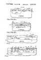
- FIG. 3shows a device of the present invention during processing
- FIG. 3Ashows a preferred manufactured product
- FIG. 4shows the first step in the preferred process of the present invention
- FIG. 5shows the gate oxide covering the active region of the left-hand bulk silicon transistor device being formed surrounded by field oxide
- FIG. 6shows the structure of FIG. 5 covered by undoped, recrystallized polysilicon
- FIG. 7shows masks 1, 2, 6, and 7
- FIG. 7Ashows masks 3, 4, and 5;
- FIG. 8shows the structure in a succeeding step in the process forming the gate for the left-hand region and the active area on the field oxide for the right-hand transistor region;
- FIG. 9shows doping of the source and drain for the left-hand transistor and doping for the right-hand transistor being developed on the field oxide
- FIG. 10depicts doping of the PMOS drain and source
- FIG. 11shows the growing of the P+ gate oxide
- FIG. 12illustrates the opening of contact regions.
- this Stacked Transistor approachhas been documented in the Background of the Invention section.
- this prior artinvolves two layers of polysilicon, i.e., the gate poly 21 and the poly layer 23.
- Poly 21comprises the gate for the first transistor and poly level 23 comprises the second transistor stacked thereabove. Since the NMOS and PMOS have poly gates the PMOS device is not self-aligned, i.e., it will require device size to density and speed compromises, however, there is no latch-up because of the elimination of the PNPN paths. Laser recrystallization of the second poly is required.
- FIGS. 3 through 12show a preferred present device and process for manufacturing the same.
- FIG. 3shows a CMOS device in process of manufacture wherein a single layer of polysilicon has been employed to form the NMOS gate 31 and the body portion 33 of the PMOS device deposited on the field oxide 35 nitride 37 being used to maintain or preserve the N-channel between the source and drain 39 and 41 (FIG. 3A) formed between the steps of FIGS. 3 and 3A.
- FIG. 3Ait may be seen that the NMOS device is formed to the left on the bulk silicon substrate 43 employing the portion 31 of the single poly layer as the gate for this device which is isolated in the cross-over oxide 45.
- the PMOS deviceutilizes another portion of the single poly layer as the source 39, drain 41, and channel 47, all situated on top of the field oxide 35.
- the present inventionoffers the only single poly layer process, which of course simplified the process and renders greater yields.
- the obvious advantage of density improvement over the ubiquitous well approachprovides scalability to submicron dimensions.
- both PMOS and NMOSare self-aligning and can be separately optimized. This improves speed and performance in general.
- By utilizing the silicon field oxide for the PMOS devicethere can be no latch-up because there is no PNPN path.
- the devicescan be reversed in position and manufactured similarly where other devices may be built in the processing according to the principles herein taught, i.e., either N-channel or P-channel can be built on the bulk silicon and two-layer enhancement depletion devices with either FET built on the bulk silicon may be accommodated.
- the silicon wafercomprises the bulk silicon 43 which is oxidized to form a first oxide layer 51 covered by a nitride layer 53 and mask 1 of FIG. 6 is used to define the active area of the left-hand transistor device, shown herein as an NMOS device.
- the resist 55protects the underlying deposited nitride layer 53 and silicon oxide layer 51 during removal of the uncovered nitride and oxide layers.
- field oxide 57is conventionally grown in the regions not covered by the resist 55.
- an underlying nitride layer 53 and oxide layer 51to expose the bare surface of silicon in the active region.
- the next stepis to grow gate oxide in the active region as is illustrated at 61 in FIG. 5.
- Step 1-Grow oxide and deposit nitride
- FIG. 6the structure of FIG. 5 has been covered by undoped polysilicon shown as the layer 63 which is subsequently recrystallized.
- the listing of the preferred processmay be updated as follows:
- Mask 1is shown at 65 as comprising the rectangular opaque outline which reserved the resist portion 55 after exposure of the resist layer to light and development thereof. Reference will be made further to these two figures as the individual masks are employed in the processing to be described hereinafter.
- the polysilicon layer 63 of FIG. 6has been doped N- everywhere and mask 2 of FIG. 7 consisting of the left-hand vertical rectangular opaque region 71 and the right-hand horizontal opaque region 72 has been utilized with conventional masking and etching techniques to outline the N gate 73 of the left-hand NMOS device being formed and the active area 75 for the right-hand PMOS device being formed on the field oxide 57.
- steps 5 through 8 of FIGS. 6 and 7has:
- Step 5deposit undoped polysilicon followed by recrystalliation
- Step 6dope the polysilicon N- everywere
- Step 7use mask 2 for laying down a resist and etching regions of the poly not covered by the resist which are;
- Step 8the N gate region for the NMOS device on the left and the active area on the field oxide for the device for the PMOS device on the right;
- mask 3 of FIG. 7ais incorporated to define the NMOS region of the left-hand device for the purpose of doping the source 81 and drain 83 N+.
- Mask 3is in reality an opening rather than being opaque, and accordingly the deposition or implanting of the N+ doping is ineffective in the field oxide 57 and merely changes the doping of the gate poly 73 from N- to N+. However, it is effective on the bare silicon to dope the source 81 and drain 83.
- the cross-over oxide or Silox 85is deposited over the entire region. Accordingly, the steps of the process now added are:
- Step 11Deposit cross-over oxide.
- mask 4 of FIG. 7Ais utilized to etch the cross-over oxide 57 from the PMOS active area 75.
- Mask 4is an open mask for the entire active area 75.
- the oxide 91is grown and a layer of nitride 93 is deposited thereover.
- mask 5 of FIG. 7Ais employed, being an opaque mask to define the PMOS gate region and to provide hardened resist thereover such that the nitride layer 93 and oxide layer 91 which are uncovered are removed.
- the PMOS source 95 and drain 97are then doped P+ by ion implantation whereas the channel region 99 is protected by the nitride 93.
- the nitride 93 and the oxide 91are removed to permit the subsequent step of oxidation over the PMOS drain-source region as shown in FIG. 11 at 101.
- Step 12use open mask 4 for etching the cross-over oxide from the P active area.
- Step 13grow oxide over region 75 and deposit nitride thereover
- Step 14use mask 5 to define the PMOS gate and remove the oxide and nitride layers except under mask 5.
- the next stepis illustrated by oxidation of the exposed field oxide 57 and the poly region 75 with the oxidation shown at 101.
- the nitride 93 and the oxide 91are removed, followed thereafter by growing the thin field oxide 103 over the gate region of the N- poly body 75.
- Step 15dope the drain and source 95 and 97 P+ (FIG. 10).
- Step 16oxidize over the P+ drain and source areas.
- Step 17remove the nitride and oxide to bare poly and grow the thin gate oxide for the PMOS device.
- the chip being processedhas been prepared for metal deposition by employing contact mask 6 of FIG. 7 to open the source 81 by opening 111, gate 73 by opening 112, and drain 83 by opening 113 through the cross-over oxide 85 for the NMOS device.
- contact mask 6 of FIG. 7to open the source 81 by opening 111, gate 73 by opening 112, and drain 83 by opening 113 through the cross-over oxide 85 for the NMOS device.
- the PMOS deviceit is only necessary to provide openings 114 and 116 to the source 95 and drain 97 because the gate 103 is already open to receive the metal deposits, which results in a metal-gate PMOS device.
- the metallization mask 7is also pictured in FIG. 7 and shows the outline of the metal conductive film preserved to connect in FIG. 3 to the metal contacts 111', 112', 113', 114' and 116'.
- the gate contact 115'is automatically provided by the metal at the location 115 of FIG. 7.
- two NMOS devicesmay be produced utilizing the process outlined for the left-hand NMOS device or similarly two PMOS devices may be produced utilizing the process outlined for the right-hand PMOS device.
- the concept of stackingsimply permits greater density of whichever devices are selected for processing and this includes self-aligned devices due to the use of mask 2.
- CMOS devicesdepletion and/or enhancement FETS or unitary assemblies.
- the gate of the first transistoris self-aligned to its drain and source by use of the poly mask 2.
- the gate of the second transistoris self-aligned to its own drain and source by virtue of mask 5.
- the single layer of polysiliconprovides the first transistor gate 73 and the active body portion 75 for the second transistor.
- Use of the mask 2defines the active body portion of the second transistor while defining the gate of the first transistor.
- mask 5defines the drain, source and gate of the second transistor by virtue of the active polysilicon portion 75. Consequently, inherent alignment is manifested between the two transistors. It should further be noted that all elements of each transistor are in linear alignment, thus, again improving the yield and conserving the space otherwise required.
Landscapes
- Metal-Oxide And Bipolar Metal-Oxide Semiconductor Integrated Circuits (AREA)
Abstract
Description
Claims (2)
Priority Applications (1)
| Application Number | Priority Date | Filing Date | Title |
|---|---|---|---|
| US06/621,773US4593453A (en) | 1982-06-01 | 1984-06-18 | Two-level transistor structures and method utilizing minimal area therefor |
Applications Claiming Priority (2)
| Application Number | Priority Date | Filing Date | Title |
|---|---|---|---|
| US38339582A | 1982-06-01 | 1982-06-01 | |
| US06/621,773US4593453A (en) | 1982-06-01 | 1984-06-18 | Two-level transistor structures and method utilizing minimal area therefor |
Related Parent Applications (1)
| Application Number | Title | Priority Date | Filing Date |
|---|---|---|---|
| US38339582ADivision | 1982-06-01 | 1982-06-01 |
Publications (1)
| Publication Number | Publication Date |
|---|---|
| US4593453Atrue US4593453A (en) | 1986-06-10 |
Family
ID=27010174
Family Applications (1)
| Application Number | Title | Priority Date | Filing Date |
|---|---|---|---|
| US06/621,773Expired - LifetimeUS4593453A (en) | 1982-06-01 | 1984-06-18 | Two-level transistor structures and method utilizing minimal area therefor |
Country Status (1)
| Country | Link |
|---|---|
| US (1) | US4593453A (en) |
Cited By (15)
| Publication number | Priority date | Publication date | Assignee | Title |
|---|---|---|---|---|
| US4740478A (en)* | 1987-01-30 | 1988-04-26 | Motorola Inc. | Integrated circuit method using double implant doping |
| US4799097A (en)* | 1987-07-29 | 1989-01-17 | Ncr Corporation | CMOS integrated devices in seeded islands |
| US4837176A (en)* | 1987-01-30 | 1989-06-06 | Motorola Inc. | Integrated circuit structures having polycrystalline electrode contacts and process |
| DE4038114A1 (en)* | 1989-11-29 | 1991-06-13 | Toshiba Kawasaki Kk | SEMICONDUCTOR STORAGE AND METHOD FOR THE PRODUCTION THEREOF |
| US5028976A (en)* | 1986-10-17 | 1991-07-02 | Canon Kabushiki Kaisha | Complementary MOS integrated circuit device |
| US5067002A (en)* | 1987-01-30 | 1991-11-19 | Motorola, Inc. | Integrated circuit structures having polycrystalline electrode contacts |
| US5072277A (en)* | 1989-07-10 | 1991-12-10 | Nippondenso Co., Ltd. | Semiconductor device with gradually varying doping levels to compensate for thickness variations |
| US5493139A (en)* | 1993-05-27 | 1996-02-20 | Sharp Kabushiki Kaisha | Electrically erasable PROM (E2 PROM) with thin film peripheral transistor |
| US5770892A (en)* | 1989-01-18 | 1998-06-23 | Sgs-Thomson Microelectronics, Inc. | Field effect device with polycrystalline silicon channel |
| US5811865A (en)* | 1993-12-22 | 1998-09-22 | Stmicroelectronics, Inc. | Dielectric in an integrated circuit |
| US5927992A (en)* | 1993-12-22 | 1999-07-27 | Stmicroelectronics, Inc. | Method of forming a dielectric in an integrated circuit |
| US6140684A (en)* | 1997-06-24 | 2000-10-31 | Stmicroelectronic, Inc. | SRAM cell structure with dielectric sidewall spacers and drain and channel regions defined along sidewall spacers |
| US6638824B2 (en) | 1998-12-28 | 2003-10-28 | Fairchild Semiconductor Corporation | Metal gate double diffusion MOSFET with improved switching speed and reduced gate tunnel leakage |
| US7078296B2 (en) | 2002-01-16 | 2006-07-18 | Fairchild Semiconductor Corporation | Self-aligned trench MOSFETs and methods for making the same |
| EP1751794A4 (en)* | 2004-05-28 | 2007-10-03 | Fairchild Semiconductor | FIELD OXIDE ENHANCEMENT METHOD AND ENHANCED FIELD OXIDE INTEGRATED CIRCUIT |
Citations (8)
| Publication number | Priority date | Publication date | Assignee | Title |
|---|---|---|---|---|
| US4057824A (en)* | 1976-04-30 | 1977-11-08 | Rca Corporation | P+ Silicon integrated circuit interconnection lines |
| US4106045A (en)* | 1975-05-20 | 1978-08-08 | The President Of The Agency Of Industrial Science And Technology | Field effect transistors |
| JPS5397384A (en)* | 1977-02-04 | 1978-08-25 | Philips Nv | Semiconductor |
| US4160260A (en)* | 1977-11-17 | 1979-07-03 | Rca Corp. | Planar semiconductor devices and method of making the same |
| JPS5562771A (en)* | 1978-11-02 | 1980-05-12 | Toshiba Corp | Integrated circuit device |
| JPS58142578A (en)* | 1982-02-19 | 1983-08-24 | Hitachi Ltd | semiconductor equipment |
| US4466172A (en)* | 1979-01-08 | 1984-08-21 | American Microsystems, Inc. | Method for fabricating MOS device with self-aligned contacts |
| US4517729A (en)* | 1981-07-27 | 1985-05-21 | American Microsystems, Incorporated | Method for fabricating MOS device with self-aligned contacts |
- 1984
- 1984-06-18USUS06/621,773patent/US4593453A/ennot_activeExpired - Lifetime
Patent Citations (8)
| Publication number | Priority date | Publication date | Assignee | Title |
|---|---|---|---|---|
| US4106045A (en)* | 1975-05-20 | 1978-08-08 | The President Of The Agency Of Industrial Science And Technology | Field effect transistors |
| US4057824A (en)* | 1976-04-30 | 1977-11-08 | Rca Corporation | P+ Silicon integrated circuit interconnection lines |
| JPS5397384A (en)* | 1977-02-04 | 1978-08-25 | Philips Nv | Semiconductor |
| US4160260A (en)* | 1977-11-17 | 1979-07-03 | Rca Corp. | Planar semiconductor devices and method of making the same |
| JPS5562771A (en)* | 1978-11-02 | 1980-05-12 | Toshiba Corp | Integrated circuit device |
| US4466172A (en)* | 1979-01-08 | 1984-08-21 | American Microsystems, Inc. | Method for fabricating MOS device with self-aligned contacts |
| US4517729A (en)* | 1981-07-27 | 1985-05-21 | American Microsystems, Incorporated | Method for fabricating MOS device with self-aligned contacts |
| JPS58142578A (en)* | 1982-02-19 | 1983-08-24 | Hitachi Ltd | semiconductor equipment |
Non-Patent Citations (4)
| Title |
|---|
| Translation of Iizuka JA55 62771.* |
| Translation of Iizuka JA55-62771. |
| Translation of Wada JA54 97384.* |
| Translation of Wada JA54-97384. |
Cited By (18)
| Publication number | Priority date | Publication date | Assignee | Title |
|---|---|---|---|---|
| US5028976A (en)* | 1986-10-17 | 1991-07-02 | Canon Kabushiki Kaisha | Complementary MOS integrated circuit device |
| US5067002A (en)* | 1987-01-30 | 1991-11-19 | Motorola, Inc. | Integrated circuit structures having polycrystalline electrode contacts |
| US4837176A (en)* | 1987-01-30 | 1989-06-06 | Motorola Inc. | Integrated circuit structures having polycrystalline electrode contacts and process |
| US4740478A (en)* | 1987-01-30 | 1988-04-26 | Motorola Inc. | Integrated circuit method using double implant doping |
| US4799097A (en)* | 1987-07-29 | 1989-01-17 | Ncr Corporation | CMOS integrated devices in seeded islands |
| US5770892A (en)* | 1989-01-18 | 1998-06-23 | Sgs-Thomson Microelectronics, Inc. | Field effect device with polycrystalline silicon channel |
| US5072277A (en)* | 1989-07-10 | 1991-12-10 | Nippondenso Co., Ltd. | Semiconductor device with gradually varying doping levels to compensate for thickness variations |
| DE4038114A1 (en)* | 1989-11-29 | 1991-06-13 | Toshiba Kawasaki Kk | SEMICONDUCTOR STORAGE AND METHOD FOR THE PRODUCTION THEREOF |
| DE4038114C2 (en)* | 1989-11-29 | 1999-03-18 | Toshiba Kawasaki Kk | Method of manufacturing a semiconductor memory |
| US5493139A (en)* | 1993-05-27 | 1996-02-20 | Sharp Kabushiki Kaisha | Electrically erasable PROM (E2 PROM) with thin film peripheral transistor |
| US5811865A (en)* | 1993-12-22 | 1998-09-22 | Stmicroelectronics, Inc. | Dielectric in an integrated circuit |
| US5927992A (en)* | 1993-12-22 | 1999-07-27 | Stmicroelectronics, Inc. | Method of forming a dielectric in an integrated circuit |
| US6140684A (en)* | 1997-06-24 | 2000-10-31 | Stmicroelectronic, Inc. | SRAM cell structure with dielectric sidewall spacers and drain and channel regions defined along sidewall spacers |
| US6638824B2 (en) | 1998-12-28 | 2003-10-28 | Fairchild Semiconductor Corporation | Metal gate double diffusion MOSFET with improved switching speed and reduced gate tunnel leakage |
| US7078296B2 (en) | 2002-01-16 | 2006-07-18 | Fairchild Semiconductor Corporation | Self-aligned trench MOSFETs and methods for making the same |
| EP1751794A4 (en)* | 2004-05-28 | 2007-10-03 | Fairchild Semiconductor | FIELD OXIDE ENHANCEMENT METHOD AND ENHANCED FIELD OXIDE INTEGRATED CIRCUIT |
| US20080113482A1 (en)* | 2004-05-28 | 2008-05-15 | Leibiger Steven M | Method for enhancing field oxide |
| US7824999B2 (en) | 2004-05-28 | 2010-11-02 | Fairchild Semiconductor Corporation | Method for enhancing field oxide |
Similar Documents
| Publication | Publication Date | Title |
|---|---|---|
| US5427964A (en) | Insulated gate field effect transistor and method for fabricating | |
| US4435895A (en) | Process for forming complementary integrated circuit devices | |
| US6790781B2 (en) | Dual depth trench isolation | |
| EP0074215B1 (en) | Cmos devices with self-aligned channel stops | |
| US5970338A (en) | Method of producing an EEPROM semiconductor structure | |
| US4306916A (en) | CMOS P-Well selective implant method | |
| EP0178440B1 (en) | Process of making dual well cmos semiconductor structure | |
| US4799098A (en) | MOS/bipolar device with stepped buried layer under active regions | |
| US6514810B1 (en) | Buried channel PMOS transistor in dual gate CMOS with reduced masking steps | |
| US4593453A (en) | Two-level transistor structures and method utilizing minimal area therefor | |
| US5032530A (en) | Split-polysilicon CMOS process incorporating unmasked punchthrough and source/drain implants | |
| US6071767A (en) | High performance/high density BICMOS process | |
| US5441906A (en) | Insulated gate field effect transistor having a partial channel and method for fabricating | |
| US6730555B2 (en) | Transistors having selectively doped channel regions | |
| US5696399A (en) | Process for manufacturing MOS-type integrated circuits | |
| US4784966A (en) | Self-aligned NPN bipolar transistor built in a double polysilicon CMOS technology | |
| US4488348A (en) | Method for making a self-aligned vertically stacked gate MOS device | |
| US5071777A (en) | Method of fabricating implanted wells and islands of cmos circuits | |
| US5005066A (en) | Self-aligned NPN bipolar transistor built in a double polysilicon CMOS technology | |
| US6303420B1 (en) | Integrated bipolar junction transistor for mixed signal circuits | |
| JPS62235769A (en) | Manufacture of transistor | |
| EP0197454A2 (en) | Method for making semiconductor devices comprising insulating regions | |
| US5830789A (en) | CMOS process forming wells after gate formation | |
| US5411900A (en) | Method of fabricating a monolithic integrated circuit with at least one CMOS field-effect transistor and one NPN bipolar transistor | |
| US5850360A (en) | High-voltage N-channel MOS transistor and associated manufacturing process |
Legal Events
| Date | Code | Title | Description |
|---|---|---|---|
| STCF | Information on status: patent grant | Free format text:PATENTED CASE | |
| FPAY | Fee payment | Year of fee payment:4 | |
| FPAY | Fee payment | Year of fee payment:8 | |
| FPAY | Fee payment | Year of fee payment:12 | |
| AS | Assignment | Owner name:CREDIT SUISSE FIRST BOSTON, NEW YORK Free format text:SECURITY INTEREST;ASSIGNORS:CONEXANT SYSTEMS, INC.;BROOKTREE CORPORATION;BROOKTREE WORLDWIDE SALES CORPORATION;AND OTHERS;REEL/FRAME:009719/0537 Effective date:19981221 | |
| AS | Assignment | Owner name:CONEXANT SYSTEMS, INC., CALIFORNIA Free format text:ASSIGNMENT OF ASSIGNORS INTEREST;ASSIGNOR:ROCKWELL SCIENCE CENTER, LLC;REEL/FRAME:010415/0761 Effective date:19981210 | |
| AS | Assignment | Owner name:CONEXANT SYSTEMS, INC., CALIFORNIA Free format text:RELEASE OF SECURITY INTEREST;ASSIGNOR:CREDIT SUISSE FIRST BOSTON;REEL/FRAME:012252/0413 Effective date:20011018 Owner name:BROOKTREE CORPORATION, CALIFORNIA Free format text:RELEASE OF SECURITY INTEREST;ASSIGNOR:CREDIT SUISSE FIRST BOSTON;REEL/FRAME:012252/0413 Effective date:20011018 Owner name:BROOKTREE WORLDWIDE SALES CORPORATION, CALIFORNIA Free format text:RELEASE OF SECURITY INTEREST;ASSIGNOR:CREDIT SUISSE FIRST BOSTON;REEL/FRAME:012252/0413 Effective date:20011018 Owner name:CONEXANT SYSTEMS WORLDWIDE, INC., CALIFORNIA Free format text:RELEASE OF SECURITY INTEREST;ASSIGNOR:CREDIT SUISSE FIRST BOSTON;REEL/FRAME:012252/0413 Effective date:20011018 | |
| AS | Assignment | Owner name:NEWPORT FAB, LLC DBA JAZZ SEMICONDUCTOR, CALIFORNI Free format text:ASSIGNMENT OF ASSIGNORS INTEREST;ASSIGNOR:CONEXANT SYSTEMS, INC.;REEL/FRAME:014337/0787 Effective date:20030623 | |
| AS | Assignment | Owner name:WACHOVIA CAPITAL FINANCE CORPORATION (WESTERN),CAL Free format text:FIRST AMENDMENT TO PATENT SECURITY AGREEMENT;ASSIGNOR:NEWPORT FAB, LLC;REEL/FRAME:019111/0295 Effective date:20070228 Owner name:WACHOVIA CAPITAL FINANCE CORPORATION (WESTERN), CA Free format text:FIRST AMENDMENT TO PATENT SECURITY AGREEMENT;ASSIGNOR:NEWPORT FAB, LLC;REEL/FRAME:019111/0295 Effective date:20070228 | |
| AS | Assignment | Owner name:NEWPORT FAB, LLC DBA JAZZ SEMICONDUCTOR OPERATING COMPANY, CALIFORNIA Free format text:RELEASE BY SECURED PARTY;ASSIGNOR:WELLS FARGO CAPITAL FINANCE, LLC, AS SUCCESSOR BY MERGER TO WACHOVIA CAPITAL FINANCE CORPORATION (WESTERN);REEL/FRAME:065284/0123 Effective date:20230929 |