US4587625A - Processor for simulating digital structures - Google Patents
Processor for simulating digital structuresDownload PDFInfo
- Publication number
- US4587625A US4587625AUS06/510,717US51071783AUS4587625AUS 4587625 AUS4587625 AUS 4587625AUS 51071783 AUS51071783 AUS 51071783AUS 4587625 AUS4587625 AUS 4587625A
- Authority
- US
- United States
- Prior art keywords
- primitive
- input
- bit
- present
- previous
- Prior art date
- Legal status (The legal status is an assumption and is not a legal conclusion. Google has not performed a legal analysis and makes no representation as to the accuracy of the status listed.)
- Expired - Lifetime
Links
Images


Classifications
- G—PHYSICS
- G06—COMPUTING OR CALCULATING; COUNTING
- G06F—ELECTRIC DIGITAL DATA PROCESSING
- G06F11/00—Error detection; Error correction; Monitoring
- G06F11/22—Detection or location of defective computer hardware by testing during standby operation or during idle time, e.g. start-up testing
- G06F11/26—Functional testing
- G06F11/261—Functional testing by simulating additional hardware, e.g. fault simulation
- G—PHYSICS
- G06—COMPUTING OR CALCULATING; COUNTING
- G06F—ELECTRIC DIGITAL DATA PROCESSING
- G06F30/00—Computer-aided design [CAD]
- G06F30/30—Circuit design
- G06F30/32—Circuit design at the digital level
- G06F30/33—Design verification, e.g. functional simulation or model checking
Definitions
- the present inventionrelates, in general, to processors for simulating and/or fault grading digital structures such as VLSI circuits. More particularly, the invention relates to a processor having an improved architecture which can economically perform simulation and fault grading of very large digital structures.
- simulationprocesses which seek to model the performance of a digital structure, such as simulation and fault grading, are referred to generically as simulation.
- a software simulatorwhich performs the simulation.
- Such software simulatorsare currently available, but would require several months to a year of dedicated CPU time to simulate a 100,000 transistor structure. This is obviously too long to be incorporated into a realistic design cycle.
- the other approachis to design a special purpose processor (hereinafter, a hardware simulator) which is loaded by a host computer with a description of the structure to be simulated, which host computer subsequently receives the results of the simulation from the hardware processor.
- a hardware simulatorwhich is loaded by a host computer with a description of the structure to be simulated, which host computer subsequently receives the results of the simulation from the hardware processor.
- the Logic Simulation Machine invented by Cocke et al.requires the dedication of an extremely complicated and costly device comprising a mainframe computer, a minicomputer and the array of basic processors for days, weeks or months at a time to perform a single simulation. Therefore, a need exists for a hardware simulator capable of performing simulations of substantially the same magnitude as the Logic Simulation Machine, but at reduced cost.
- Yet a further object of the present inventionis to provide a hardware simulator utilizing an advanced primitive and an improved primitive evaluation architecture.
- Still a further object of the inventionis to provide a hardware simulator capable of handling very large digital structures utilizing a single processor.
- a preferred embodiment of the present inventioncomprises a hardware simulator for use with a mini-computer host.
- the simulatorcomprises a single, special purpose processor which simulates a structure described in terms of an advanced primitive.
- the advanced primitivehas four inputs and a single output and is capable of representing memory cells as well as simpler logic devices.
- the primitive evaluation processconsiders previous as well as present input states.
- the state of each location, or node, within the structureis represented by a three-bit word having five permitted values.
- a highly efficient primitive evaluation architecture and bus resolver logicdetermine the output state of a given primitive in a minimum number of clock cycles.
- the state memory of the processorincludes the present and previous state of each node in the structure, allowing the evaluation of the advanced primitive.
- the structure descriptionis contained in a writable control store, which provides state memory and primitive evaluator addresses as a program counter is stepped through the structure.
- the state memoryutilizes a ping-pong architecture to avoid the necessity of ordering the structure to be simulated.
- the preferred embodiment of the present inventionis designed to simulate a structure comprising 64K advanced primitives, which corresponds to a circuit including up to approximately 250,000 transistors.
- the processoris intended to be loaded with the structure description and input vector by a dedicated mini-computer host, such as an EXORmacs® development system, which receives the output vector at the conclusion of the simulation.
- a dedicated mini-computer hostsuch as an EXORmacs® development system, which receives the output vector at the conclusion of the simulation.
- the system describedis intended to offer the level of performance similar to other hardware or software simulators at roughly one-tenth the cost, thus allowing the dedication of a single unit to a particular task for the long periods required to simulate very large digital structures.
- FIG. 1is a block diagram of a processor useful for simulating digital structures according to the principles of the present invention
- FIG. 2is a detailed block diagram of a writable control store portion of a simulator processor according to the principles of the present invention
- FIG. 3is a detailed block diagram of a state memory portion of a simulator processor according to the principles of the present invention.
- FIG. 4is a detailed block diagram of a primitive evaluator portion of a simulator processor according to the principles of the present invention
- FIG. 5is a flowchart describing the resolution function of the bus resolver portion of the primitive evaluator of FIG. 4;
- FIG. 6is a timing diagram used to describe the simulation of a two input flip-flop.
- the advanced primitive around which the simulator processor according to the principles of the present invention is designedis a four-input, one-output device which has one possible internal history element.
- the advanced primitiveis capable, by itself, of representing a flip flop or memory cell which would require two or more primitives without an internal history element.
- the structure of the simulator processorallows for 512 different primitive types with which to describe the digital structure to be simulated.
- the functional description of the various primitive types and the compilation of the description of the digital structure in terms of the primitivestake place within a host computer system to which the simulator processor is connected.
- a nodecorresponds to the output of one or more primitives and to an input of one or more primitives.
- a nodemay also represent a point of input or output to the digital structure.
- each nodeis identified by the processor by the number of the primitive at whose output the node is located.
- the simulator processoris a five-state machine. In other words, it requires three bits to specify the state of any node in the digital structure. These three bits are referred to as the data bit, the Z bit and the X bit; or A0, A1 and A2, respectively.
- the five possible states which may be assumed by any node within the digital structure and the corresponding bit patternare found in Table I. All bit patterns other than those found in Table I are prohibited.
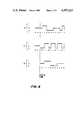
- a simulator processor 10controls the running of the simulation by sequentially stepping through the primitives which are used to describe the digital structure.
- program counter 11supplies a sequential address, or primitive number, to a writable control store (WCS) 12.
- WCSwritable control store
- Program counter 11also supplies an evaluation write address to a state memory (SM) 13.
- the evaluation write addresscorresponds to the location in state memory 13 of the node which is at the output of the current primitive.
- nodesare identified by the number of the primitive at whose output the node appears.
- the evaluation write addresswhich locates the output node of the current primitive, is identical to the primitive number supplied to WCS 12.
- writable control store 12When writable control store 12 receives a new primitive number from program counter 11 it supplies, by means of lines 14, the read addresses for the locations in state memory 13 of the nodes which are at the inputs of the current primitive. Writable control store 12 also supplies, by means of line 15, a primitive type indicator to a primitive evaluator 16.
- state memory 13Once state memory 13 has received the read addresses for the inputs of the current primitive from writable control store 12, it reads the current states of those nodes and communicates that information to primitive evaluator 16 via line 17. Since primitive evaluator 16 now has an indication of the type of the current primitive and the states of all of the inputs thereof, it can evaluate the current state of the output thereof. This is communicated to state memory 13 by means of line 18 and is written in the location specified by the evaluation write address.
- each of the major components of simulator processor 10has an input channel from the host computer system 19. This allows the description of the digital structure to be entered prior to simulation along with the states of the input points of the structure.
- the host computer system 19provides the functional descriptions of the various primitive types to be used in the simulation and may also provide for the alteration, or faulting, of various nodes in the structure. Further, host computer system 19 receives the output of primitive evaluator 16 as an input.
- simulator processor 10is designed to simulate digital structures which are described with up to 64K primitives.
- each of the lines which specify a particular primitive within the structureis a 16 bit line.
- line 15, which carries a primitive type indicatoris a 9-bit line.
- the processoris basically a two cycle device. During one cycle the input states of a primitive are assembled by state memory 13. During the next cycle the primitive is evaluated. During both cycles the read addresses for the next primitive are being accessed in writable control store 12. Furthermore, the architecture of state memory 13 allows the result of the previous evaluation to be written while the inputs for the current primitive are being assembled.
- a simulator processoraccording to the principles of the present invention will be capable of performing as many as four million complete primitive evaluations per second.
- Program counter 11steps through each primitive in the structure repeatedly until the structure settles down or until an oscillation state is identified. It is anticipated that very large digital structures may be simulated in a matter of a few seconds.
- writable control store 12comprises a primitive type block 22 and four input read address blocks 23, 24, 25 and 26.
- Each of the blocks 22-26 which make up writable control store 12is a block of memory which is 64K bits deep.
- Primitive type block 22is nine bits wide and each of the input read address blocks 23-26 is 16 bits wide.
- a 16-bit sequential address, or primitive number, line 27couples the address input of each of the blocks 22-26 to the program counter. Each time the program counter steps to the next sequential primitive number primitive type block 22 puts an indicator of primitive type of the current primitive on 9-bit line 15.
- Each of the input read address blocks 23-26puts a 16 bit address indicating the location in state memory of the node corresponding to that input of the current primitive on one of lines 14.
- input 1 read address block 23provides the address in state memory at which the current state of the node corresponding to input 1 of the current primitive can be found.
- writable control store 12can be readily constructed from standard memory parts. Since the details of the construction will depend upon the particular parts chosen, they will not be discussed herein.
- state memory 13is shown in a detailed block diagram.
- State memory 13primarily comprises an A portion 30, a B portion 31 and a previous state portion 32.
- a portion 30 and B portion 31contain the information regarding the states of the nodes at the inputs of the current primitive and regarding the history of the input states of the current primitive necessary for primitive evaluator 16 to resolve the output state of the current primitive.
- the required informationis read from A portion 30.
- the output informationis written into B portion 31.
- the roles of the A and B portionsare swapped and the evaluation of each primitive is repeated. This is referred to as a ping-pong memory management scheme.
- the newly resolved output state of each primitiveis compared to the previous state of that primitive as is stored in previous state portion 32. If an entire pass through each of the primitives is completed showing agreement between the previous and present states of each primitive, the simulation is declared complete. It is also possible to declare, after a predetermined number of passes through each of the primitives, that a state of oscillation exists in the digital structure being simulated.
- the ping-pong memory management schemeis implemented by means of switch 42 and multiplexer 43.
- multiplexer 43selects the information read from A portion 30 to be passed to the primitive evaluator and switch 42 couples the results produced by primitive evaluator 16 to B block 31 to be written.
- multiplexer 43selects the information read from B portion 31 to be passed to primitive evaluator 16 and switch 42 couples the results to A portion 30 to be written.
- a portion 30comprises an input 1A block 33A, an input 2A block 34A, an input 3A block 35A, an input 4A block 36A, a previous data bit A block 37A and a previous X bit A block 38A.
- Input 1A block 33Ais a block of memory 64K bits deep and two bits wide. It stores, at each of its 64K locations, the data bit and the X bit which specify the state of the node at the output of one of the primitives in the digital structure.
- input 2A block 34Ais a block of memory 64K bits deep and two bits wide and stores the data bits and X bits which specify the states of the nodes at the outputs of each of the primitives.
- Input 3A block 35Ais a block of memory 64K bits deep and two bits wide and stores the data bits and the X bits which specify the states of the nodes at the outputs of each of the primitives.
- input 4A block 36Ais a block of memory 64K bits deep and three bits wide and it stores the data bits, the Z bits and the X bits which specify the states of the nodes at the outputs of each of the primitives. It has been found that sufficient flexibility in specifying primitive function can be achieved with only one input of the primitive being specified with three bits. For simplicity, this is always defined as input 4, and the other inputs are specified using two bits.
- Previous data bit A block 37Ais a block of memory 64K bits deep and four bits wide and it stores the data bits from each of the four inputs of each primitive during the immediately preceding pass through the structure.
- previous X bit A block 38Ais a block of memory 64K bits deep and four bits wide and stores the X bit from each of the four inputs of each primitive during the immediately preceding pass through the structure.
- the appropriate locations in input blocks 33A, 34A, 35A and 36Aare selected by the addresses on lines 14 which were supplied by writable control store 12.
- the address supplied to input 1A block 33Aidentifies the primitive whose output is coupled to input 1 of the current primitive.
- the informationis addressed sequentially, or by primitive number. This is supplied by a sequential address line 39 which carries the 16-bit primitive number of the current primitive.
- the address which specifies the location at which the results of the evaluation of the current primitive are to be writtenis supplied to blocks 33A, 34A, 35A and 36A by write address line 40.
- the address on line 40is identical to the sequential address, or primitive number, on line 39.
- the resolved state of the output of the current primitiveis coupled to switch 42 from primitive evaluator 16 via resolved bus 47. Since A portion 30 is being written to in this pass, switch 42 couples the 3-bit output state to line 41A. This information is written into blocks 33A, 34A, 35A and 36A at the location specified by line 40. In the case of blocks 33A, 34A and 35A, only the data bit and X bit are written.
- the data bits which appeared at each of the inputs of the current primitive during the current evaluation passare coupled from primitive evaluator 16 through switch 42 and line 45A to be written in previous data bit A block 37A at the address specified by line 39.
- the X bits appearing at each of the four inputs of the current primitive during the current passare coupled from primitive evaluator 16 through switch 42 and line 46A to previous X bit A block 38A to be written in the location specified by line 39.
- previous state portion 32is a block of memory which is 64K bits long and three bits wide.
- the addresses which must be supplied by writable control store 12 via lines 14are simply the sequential primitive numbers of the primitives whose outputs are coupled to the four inputs of the current primitive.
- block 23 of writable control store 12supplies the 16 bit equivalent of the number N to input 1A block 33A of state memory 13 when program counter 11 advances to primitive number M.
- the appropriate addresseswere loaded into writeable control store 12 via the link to the host computer system.
- FIG. 3omits the link between state memory 13 and the host computer system. As is apparent, this link allows the host computer system to determine the contents of state memory 13 prior to starting a simulation. The generation of an input vector, which specifies the states of the input points of the digital structure, and the loading of the input vector into state memory 13 are accomplished on the host computer system.
- a 17-bit line 53 from multiplexer 43 of state memory 13is split into four lines 54, 55, 56 and 57.
- Line 54is a 5-bit line carrying the present data bit from each of the four inputs to the current primitive and the Z bit from input 4 of the current primitive.
- Line 55is a 4-bit line carrying the data bits from all four inputs of the current primitive during the immediately preceding pass through the structure.
- Line 56is a 4-bit line carrying the present X bits from all four inputs of the current primitive.
- Line 57is a 4-bit line carrying all four X bits from the input of the current primitive during the immediately preceding pass through the structure.
- Lines 54, 55, 56 and 57are coupled to an input bus controller 58.
- Input bus controller 58is used to artificially control the inputs to primitive evaluator 16 under control of the host computer system, regardless of the information stored in state memory 13. For instance, during the first pass through the structure, input bus controller 58 may be used to generate unknown states, or X states, in all locations except those occupied by the input vector. This may be more efficient than storing X states in all locations in state memory 13 prior to starting the simulation. More importantly, input bus controller 58 may be used to introduce faults into the digital structure at any given point during the simulation for fault grade purposes.
- the next stage of primitive evaluator 16comprises a primitive table 59, a data bit history table 60, a present X table 61 and an X history table 62.
- Each of the tables 59, 60, 61 and 62is actually 512 tables corresponding to the 512 available primitive types.
- the correct one of each of the tablesis selected by the 9-bit primitive type indicator on line 15, which is coupled to each table.
- a line 63 from input bus controller 58 carrying the four data bits which presently appear at the inputs of the current primitiveis coupled to each of the tables 59, 60, 61 and 62.
- Tables 59, 60, 61 and 62are used to answer four questions regarding the current and previous states of the primitive inputs. The answers to these questions depend upon the functional description of the particular primitive type. The answers can be used to unambiguously determine the current output state of the primitive. This architecture represents a significant advance in the evaluation efficiency of hardware simulators.
- the four questions to be answeredare: (1) is the primitive leaving an X condition; (2) does the primitive presently have an X condition at an input; (3) has the primitive transitioned properly; and (4) what is the new result.
- X history table 62present X table 61, data bit history table 60 and primitive table 59, respectively. The details of the evaluation process are discussed more fully below.
- Primitive table 59is input with the Z bit from input 4 of the current primitive by means of line 70 from input bus controller 58.
- Data bit history table 60is input with the four previous data bits from the inputs of the primitive by means of line 71 from input bus controller 58.
- Present X table 61is input with the four present X bits from the inputs from the primitive by means of line 72 from input bus controller 58.
- X history table 62is input with the four previous X bits from the inputs of the primitive by means of line 73 from input bus controller 58.
- the outputs of tables 59, 60, 61 and 62are coupled by means of lines 75, 76, 77 and 78, respectively, to bus resolver logic 64.
- Bus resolver logic 64also has inputs coupled to line 48 from previous state memory portion 32 of state memory 13, to present X bit line 56 and to the four present data bits on line 54. According to a process discussed fully below, bus resolver logic 64 determines the current output state of the current primitive and passes the result by means of line 47 to state memory 13. It also passes the four present data bits by means of line 65 to be stored in previous data bit memory. Also, the four present X bits are passed via line 66 to be stored in previous X bit memory.
- X history table 62produces a two-bit output the definition of which is described in Table II.
- X history table 62is only defined for proper operation when no present X conditions exist. As will be described later, bus resolver logic 64 detects present X conditions and, if appropriate, ignores the output of X history table 62.
- present X table 61produces a two-bit output the definition of which is contained in Table II, above.
- Data bit history table 60produces a three-bit output, of which two bits are defined according to Table III.
- the third bit output by data bit history table 60is used in implementing the conditional X function of the evaluator. This function will be described below in the discussion of bus resolver logic 64.
- bus resolver logic 64is responsible for receiving the outputs of tables 59, 60, 61 and 62 and resolving the current output state of the current primitive therefrom. The logical process by which this result is achieved is described with reference to FIG. 5. First, bus resolver logic 64 determines, from the contents of present X bit line 56, whether there is presently an X condition at one of the inputs of the primitive. If the answer is yes, this indicates that the output of X history table 62 is not necessarily correct and bus resolver logic 64 branches around its consideration of the output of X history table 62. If there is no X condition presently occurring, bus resolver logic 64 proceeds to consider the output of X history table 62.
- the output state of the current primitiveis resolved to be X and resolver logic 64 outputs on resolved bus 47 the three-bit code corresponding to an X state as defined in Table I. If the output of X history table 62 is conditional X, then a "save conditional" operation is performed and bus resolver logic proceeds to the consideration of the output of present X table 61. If the output of X history table 62 is no action, then the consideration of the output of present X table 61 begins immediately.
- bus resolver logic 64checks to see if the third bit produced by data bit history table 60 is set to 1, indicating that previous conditional X results should be acted upon. If bit #3 is equal to one, then a check for previously saved conditional X results is made. If one is found, then an absolute X result is given and the evaluation is terminated. If either of the checks results in a negative answer, then the remainder of data bit history table output is considered.
- bus resolver logic 64resolves the current output state of the primitive to be identical to the previous output state of that primitive and simply transfers the three-bit code on line 48 to resolved bus 47.
- the result of a no-action output from data bit history table 60is that the consideration of the output of primitive table 59 proceeds.
- bus resolver logicmust consider the value of the third bit, or conditional X bit, produced by data bit history table 60.
- bus resolver logic 64proceeds to consider the output of primitive table 59.
- Primitive table 59can produce an absolute X output, whose result is the same as was described above.
- primitive table 59can produce the "0", “1", “Z0” and “Z1” results, in which case the appropriate three-bit codes are placed on resolved bus 47.
- bus resolver logic 64is responsible for comparing the newly resolved output state of the current primitive to the previously resolved state which is present on line 48. If an entire pass through the structure as defined by the primitives results in complete agreement between the current and previous states of each of the primitives, then the simulation is declared complete. It is also possible to define an oscillation condition in which a predetermined number of passes through the structure are completed without achieving a settled condition. Through its link to the host computer system, bus resolver logic 64 can be used to insert faults in the system in much the same way as input bus controller 58.
- FIG. 6In order to more fully understand the function of the primative evaluator of FIG. 4, the reader is referred to FIG. 6 and the tables below. These will be used in describing the manner in which the primitive evaluator of FIG. 4 operates during the simulation of a flip-flop circuit.
- a flip-flopis chosen because it is a relatively complex device from the standpoint of a simulator. For instance, typical prior art simulators using simple primitives require 10 primitives to simulate one flip-flop, whereas a single advanced primitive according to the principles of the present invention is sufficient.
- the flip-flopis assumed to have only data (D) and clock (C) inputs.
- the single outputis designated Q. In the example illustrated, only the data and X bits must be considered in performing the evaluation.
- a subscript X on either the D or Cindicates that the X bit of that particular input is given in that column of the table. Similarly, a superscript -1 indicates that the previous, as opposed to the present, bits are in that column.
- an X stateis arbitrarily shown to have a level lying between the 1 level and 0 level.
- the present and past states of both the D and C inputsare defined to be X states prior to the beginning of the simulation as shown in FIG. 6.
- the D inputremains in an X state and the C input is in a 0 state.
- the X history tablewill be by-passed due to the presence of an X state at the D input.
- the output of the present X tableis considered. Since the D input is in an X state, the X bit is equal to 1 and the data bit is equal to 0. Since the C input is in a 0 state, the X bit is equal to 0 and the data bit is equal to 0. This provides the location in the present X table, which is designated (1000), at which the output of the present X table can be found. As indicated, that output is no action (NA).
- the data bit history tableis considered next. Since both inputs were previously in an X state, the previous data bits are both equal to 0. Again, the current data bits are 0 and 0. Thus, the output of the data bit history table is Q-1. This indicates that the previous output state is to be used as the present output state. Since the previous output state is undefined, the present output state is X. The fact that bit number 3 produced by the data bit history table is equal to 1 is not considered, since no conditional X's were produced earlier. Since a Q-1 result was reached in the data bit history table, the primitive table is not consulted.
- a conditional X resultis received from the present X table. This is a result of the fact that the present D input is in an X state. However, the data bit history table produces a Q-1 output together with a third bit of 0. Since the third bit was not equal to 1, the conditional X is ignored and the resolved state is "0".
- a conditional Xis again produced by the present X table and the data bit history table produces a no action coupled with a third bit of 1. This third bit value triggers the activation of the conditional X and results in an absolute X output.
Landscapes
- Engineering & Computer Science (AREA)
- Computer Hardware Design (AREA)
- Theoretical Computer Science (AREA)
- Physics & Mathematics (AREA)
- General Engineering & Computer Science (AREA)
- General Physics & Mathematics (AREA)
- Evolutionary Computation (AREA)
- Geometry (AREA)
- Quality & Reliability (AREA)
- Management, Administration, Business Operations System, And Electronic Commerce (AREA)
Abstract
Description
The present invention relates, in general, to processors for simulating and/or fault grading digital structures such as VLSI circuits. More particularly, the invention relates to a processor having an improved architecture which can economically perform simulation and fault grading of very large digital structures.
During the design of very large digital structures, such as VLSI circuits comprising upwards of 100,000 transistors, it is crucial to have available relatively quick means for simulating the performance of a current version of the structure. In addition, it is sometimes necessary to perform rigorous fault grading of a proposed structure; that is, to accurately determine the effects of a particular failure within the structure. Hereinafter, all processes which seek to model the performance of a digital structure, such as simulation and fault grading, are referred to generically as simulation.
One approach to the problem is to devise a program to be run on a general purpose computer (hereinafter, a software simulator) which performs the simulation. Such software simulators are currently available, but would require several months to a year of dedicated CPU time to simulate a 100,000 transistor structure. This is obviously too long to be incorporated into a realistic design cycle.
The other approach is to design a special purpose processor (hereinafter, a hardware simulator) which is loaded by a host computer with a description of the structure to be simulated, which host computer subsequently receives the results of the simulation from the hardware processor.
An example of such a hardware processor is described in U.S. Pat. No. 4,306,286, issued to John Cocke et al. on Dec. 15, 1981. This device, designated a Logic Simulation Machine by its inventors, is a very large device comprising a plurality of highly parallel basic processors which are interconnected by means of a switch and a local computer, which is coupled to a mainframe host computer. In the described embodiment, each basic processor simulates 1K (1024) gates. Each gate, also referred to as a primitive, is the basic functional unit with which the structure is described and has 5 inputs and 1 output. While any digital structure can be simulated with very simple primitives (e.g. the Boolean Functions AND, OR and XOR), more primitives are required to describe a given structure if each is excessively simple. The Logic Simulation Machine invented by Cocke et al. requires the dedication of an extremely complicated and costly device comprising a mainframe computer, a minicomputer and the array of basic processors for days, weeks or months at a time to perform a single simulation. Therefore, a need exists for a hardware simulator capable of performing simulations of substantially the same magnitude as the Logic Simulation Machine, but at reduced cost.
Accordingly, it is an object of the present invention to provide an improved processor for simulating digital structures.
It is a further object to provide an improved hardware simulator.
Yet a further object of the present invention is to provide a hardware simulator utilizing an advanced primitive and an improved primitive evaluation architecture.
Still a further object of the invention is to provide a hardware simulator capable of handling very large digital structures utilizing a single processor.
A preferred embodiment of the present invention comprises a hardware simulator for use with a mini-computer host. The simulator comprises a single, special purpose processor which simulates a structure described in terms of an advanced primitive. The advanced primitive has four inputs and a single output and is capable of representing memory cells as well as simpler logic devices. In other words, the primitive evaluation process considers previous as well as present input states. The state of each location, or node, within the structure is represented by a three-bit word having five permitted values. A highly efficient primitive evaluation architecture and bus resolver logic determine the output state of a given primitive in a minimum number of clock cycles. The state memory of the processor includes the present and previous state of each node in the structure, allowing the evaluation of the advanced primitive. The structure description is contained in a writable control store, which provides state memory and primitive evaluator addresses as a program counter is stepped through the structure. The state memory utilizes a ping-pong architecture to avoid the necessity of ordering the structure to be simulated.
The preferred embodiment of the present invention is designed to simulate a structure comprising 64K advanced primitives, which corresponds to a circuit including up to approximately 250,000 transistors. The processor is intended to be loaded with the structure description and input vector by a dedicated mini-computer host, such as an EXORmacs® development system, which receives the output vector at the conclusion of the simulation. The system described is intended to offer the level of performance similar to other hardware or software simulators at roughly one-tenth the cost, thus allowing the dedication of a single unit to a particular task for the long periods required to simulate very large digital structures.
These and other objects and advantages of the present invention will be apparent to one skilled in the art from the detailed description below taken together with the drawings.
FIG. 1 is a block diagram of a processor useful for simulating digital structures according to the principles of the present invention;
FIG. 2 is a detailed block diagram of a writable control store portion of a simulator processor according to the principles of the present invention;
FIG. 3 is a detailed block diagram of a state memory portion of a simulator processor according to the principles of the present invention;
FIG. 4 is a detailed block diagram of a primitive evaluator portion of a simulator processor according to the principles of the present invention;
FIG. 5 is a flowchart describing the resolution function of the bus resolver portion of the primitive evaluator of FIG. 4; and
FIG. 6 is a timing diagram used to describe the simulation of a two input flip-flop.
Digital structures which are to be simulated using the processor disclosed herein are described in terms of basic functional units referred to primitives. The advanced primitive around which the simulator processor according to the principles of the present invention is designed is a four-input, one-output device which has one possible internal history element. In other words, the advanced primitive is capable, by itself, of representing a flip flop or memory cell which would require two or more primitives without an internal history element. In the preferred embodiment of the present invention the structure of the simulator processor allows for 512 different primitive types with which to describe the digital structure to be simulated. The functional description of the various primitive types and the compilation of the description of the digital structure in terms of the primitives take place within a host computer system to which the simulator processor is connected. These processes are well within the knowledge of one skilled in the art of using hardware or software simulators and will not be discussed in detail herein.
Besides the primitives, the other structural features of the digital structure which are discussed herein are the nodes, or the locations within the digital structure the state of which is stored in state memory. In general, a node corresponds to the output of one or more primitives and to an input of one or more primitives. A node may also represent a point of input or output to the digital structure. As will be apparent from the description of the state memory architecture below, each node is identified by the processor by the number of the primitive at whose output the node is located.
In the preferred embodiment of the present invention the simulator processor is a five-state machine. In other words, it requires three bits to specify the state of any node in the digital structure. These three bits are referred to as the data bit, the Z bit and the X bit; or A0, A1 and A2, respectively. The five possible states which may be assumed by any node within the digital structure and the corresponding bit pattern are found in Table I. All bit patterns other than those found in Table I are prohibited.
TABLE I ______________________________________ DATA X BIT Z BIT BIT A2 A1 A0 VALUE DESCRIPTION ______________________________________ 0 0 0 "0" DrivenLow Level 0 0 1 "1" DrivenHigh Level 0 1 0 "Z0" UndrivenLow Level 0 1 1 "Z1" UndrivenHigh Level 1 0 0 "X" Unknown Value ______________________________________
Referring now to FIG. 1, asimulator processor 10 according to the principles of the present invention is shown in a simplified block diagram. A program counter (PC) 11 controls the running of the simulation by sequentially stepping through the primitives which are used to describe the digital structure. At each step,program counter 11 supplies a sequential address, or primitive number, to a writable control store (WCS) 12.Program counter 11 also supplies an evaluation write address to a state memory (SM) 13. The evaluation write address corresponds to the location instate memory 13 of the node which is at the output of the current primitive. In the preferred embodiment, nodes are identified by the number of the primitive at whose output the node appears. Thus, the evaluation write address, which locates the output node of the current primitive, is identical to the primitive number supplied toWCS 12. Whenwritable control store 12 receives a new primitive number fromprogram counter 11 it supplies, by means oflines 14, the read addresses for the locations instate memory 13 of the nodes which are at the inputs of the current primitive.Writable control store 12 also supplies, by means ofline 15, a primitive type indicator to aprimitive evaluator 16. Oncestate memory 13 has received the read addresses for the inputs of the current primitive fromwritable control store 12, it reads the current states of those nodes and communicates that information toprimitive evaluator 16 vialine 17. Sinceprimitive evaluator 16 now has an indication of the type of the current primitive and the states of all of the inputs thereof, it can evaluate the current state of the output thereof. This is communicated tostate memory 13 by means ofline 18 and is written in the location specified by the evaluation write address.
As shown in FIG. 1, each of the major components ofsimulator processor 10 has an input channel from thehost computer system 19. This allows the description of the digital structure to be entered prior to simulation along with the states of the input points of the structure. In addition, thehost computer system 19 provides the functional descriptions of the various primitive types to be used in the simulation and may also provide for the alteration, or faulting, of various nodes in the structure. Further,host computer system 19 receives the output ofprimitive evaluator 16 as an input.
In the preferred embodiment of the presentinvention simulator processor 10 is designed to simulate digital structures which are described with up to 64K primitives. Thus, each of the lines which specify a particular primitive within the structure is a 16 bit line. Since 512 primitive types are to be accommodated,line 15, which carries a primitive type indicator, is a 9-bit line. As will be more apparent from the descriptions of the various elements of the simulator processor, the processor is basically a two cycle device. During one cycle the input states of a primitive are assembled bystate memory 13. During the next cycle the primitive is evaluated. During both cycles the read addresses for the next primitive are being accessed inwritable control store 12. Furthermore, the architecture ofstate memory 13 allows the result of the previous evaluation to be written while the inputs for the current primitive are being assembled. It is anticipated that a simulator processor according to the principles of the present invention will be capable of performing as many as four million complete primitive evaluations per second. Program counter 11 steps through each primitive in the structure repeatedly until the structure settles down or until an oscillation state is identified. It is anticipated that very large digital structures may be simulated in a matter of a few seconds.
Referring now to FIG. 2,writable control store 12 is shown in a detailed block diagram.Writable control store 12 comprises aprimitive type block 22 and four input read address blocks 23, 24, 25 and 26. Each of the blocks 22-26 which make upwritable control store 12 is a block of memory which is 64K bits deep.Primitive type block 22 is nine bits wide and each of the input read address blocks 23-26 is 16 bits wide. A 16-bit sequential address, or primitive number,line 27 couples the address input of each of the blocks 22-26 to the program counter. Each time the program counter steps to the next sequential primitive numberprimitive type block 22 puts an indicator of primitive type of the current primitive on 9-bit line 15. Each of the input read address blocks 23-26 puts a 16 bit address indicating the location in state memory of the node corresponding to that input of the current primitive on one oflines 14. In other words,input 1read address block 23 provides the address in state memory at which the current state of the node corresponding to input 1 of the current primitive can be found. The input from the host computer system towritable control store 12, which is not shown in FIG. 2, simply provides a means for writing information to each of the memory locations inwritable control store 12. As is apparent to one skilled in the art,writable control store 12 can be readily constructed from standard memory parts. Since the details of the construction will depend upon the particular parts chosen, they will not be discussed herein.
Referring now to FIG. 3,state memory 13 is shown in a detailed block diagram.State memory 13 primarily comprises anA portion 30, aB portion 31 and aprevious state portion 32. As will be more apparent from the detailed discussion below, Aportion 30 andB portion 31 contain the information regarding the states of the nodes at the inputs of the current primitive and regarding the history of the input states of the current primitive necessary forprimitive evaluator 16 to resolve the output state of the current primitive. At the start of the simulation process, the required information is read from Aportion 30. As each primitive is resolved, the output information is written intoB portion 31. When each of the primitives has been evaluated once, the roles of the A and B portions are swapped and the evaluation of each primitive is repeated. This is referred to as a ping-pong memory management scheme. At each stage, the newly resolved output state of each primitive is compared to the previous state of that primitive as is stored inprevious state portion 32. If an entire pass through each of the primitives is completed showing agreement between the previous and present states of each primitive, the simulation is declared complete. It is also possible to declare, after a predetermined number of passes through each of the primitives, that a state of oscillation exists in the digital structure being simulated.
The ping-pong memory management scheme is implemented by means ofswitch 42 andmultiplexer 43. In other words, on one pass,multiplexer 43 selects the information read from Aportion 30 to be passed to the primitive evaluator and switch 42 couples the results produced byprimitive evaluator 16 to B block 31 to be written. On the next pass through the primitives,multiplexer 43 selects the information read fromB portion 31 to be passed toprimitive evaluator 16 and switch 42 couples the results to Aportion 30 to be written.
In order for this scheme to work, the structure of Aportion 30 andB portion 31 must be identical. Therefore, only Aportion 30 will be described in detail.
Aportion 30 comprises aninput 1A block 33A, aninput 2A blockinput 3A blockinput 4A blockblock 37A and a previous X bit Ablock 38A.Input 1A block 33A is a block ofmemory 64K bits deep and two bits wide. It stores, at each of its 64K locations, the data bit and the X bit which specify the state of the node at the output of one of the primitives in the digital structure. Similarly,input 2A blockmemory 64K bits deep and two bits wide and stores the data bits and X bits which specify the states of the nodes at the outputs of each of the primitives.Input 3A blockmemory 64K bits deep and two bits wide and stores the data bits and the X bits which specify the states of the nodes at the outputs of each of the primitives. Finally,input 4A blockmemory 64K bits deep and three bits wide and it stores the data bits, the Z bits and the X bits which specify the states of the nodes at the outputs of each of the primitives. It has been found that sufficient flexibility in specifying primitive function can be achieved with only one input of the primitive being specified with three bits. For simplicity, this is always defined asinput 4, and the other inputs are specified using two bits.
Previous data bit Ablock 37A is a block ofmemory 64K bits deep and four bits wide and it stores the data bits from each of the four inputs of each primitive during the immediately preceding pass through the structure. Similarly, previous X bit Ablock 38A is a block ofmemory 64K bits deep and four bits wide and stores the X bit from each of the four inputs of each primitive during the immediately preceding pass through the structure.
During a pass in which Ablock 30 is being read from, the appropriate locations in input blocks 33A, 34A, 35A and 36A are selected by the addresses onlines 14 which were supplied bywritable control store 12. In other words, the address supplied to input1A block 33A identifies the primitive whose output is coupled toinput 1 of the current primitive. In the case ofblocks sequential address line 39 which carries the 16-bit primitive number of the current primitive.
Once the individual data blocks in Aportion 30 have been supplied with the appropriate addresses, the 17 bits which make up the combined outputs of the individual blocks are placed online 44A which couples Aportion 30 tomultiplexer 43. Since Aportion 30 is being read from during this pass,multiplexer 43 will select the 17 bits online 44A to be passed to the primitive evaluator.
During a pass in which Aportion 30 is being written to, the address which specifies the location at which the results of the evaluation of the current primitive are to be written is supplied toblocks write address line 40. As was discussed above, the address online 40 is identical to the sequential address, or primitive number, online 39. The resolved state of the output of the current primitive is coupled to switch 42 fromprimitive evaluator 16 via resolvedbus 47. Since Aportion 30 is being written to in this pass, switch 42 couples the 3-bit output state to line 41A. This information is written intoblocks line 40. In the case ofblocks primitive evaluator 16 throughswitch 42 andline 45A to be written in previous data bit Ablock 37A at the address specified byline 39. The X bits appearing at each of the four inputs of the current primitive during the current pass are coupled fromprimitive evaluator 16 throughswitch 42 andline 46A to previous X bit Ablock 38A to be written in the location specified byline 39. As is apparent, by the time this information is read during the next evaluation pass, it will be the previous bit information which is required.
The resolved state of the output of the current primitive is coupled fromprimitive evaluator 16 toprevious state portion 32 by means of resolvedbus 47 and is written in the location specified bysequential address line 39. When program counter 11 steps to a new primitive number, this will appear onsequential address line 39 and the previous output state of the current primitive will be read fromprevious state portion 32 and passed toprimitive evaluator 16 vialine 48. As is apparent,previous state portion 32 is a block of memory which is 64K bits long and three bits wide.
As will be apparent to one skilled in the art from the detailed description of the architecture ofstate memory 13, the addresses which must be supplied bywritable control store 12 vialines 14 are simply the sequential primitive numbers of the primitives whose outputs are coupled to the four inputs of the current primitive. In other words, if primitive number M hasinput 1 coupled to the output of primitive number N, then block 23 ofwritable control store 12 supplies the 16 bit equivalent of the number N to input 1A block 33A ofstate memory 13 when program counter 11 advances to primitive number M. As was discussed above, the appropriate addresses were loaded intowriteable control store 12 via the link to the host computer system.
FIG. 3 omits the link betweenstate memory 13 and the host computer system. As is apparent, this link allows the host computer system to determine the contents ofstate memory 13 prior to starting a simulation. The generation of an input vector, which specifies the states of the input points of the digital structure, and the loading of the input vector intostate memory 13 are accomplished on the host computer system.
Referring now to FIG. 4,primitive evaluator 16 is shown in a detailed block diagram. A 17-bit line 53 frommultiplexer 43 ofstate memory 13 is split into fourlines Line 54 is a 5-bit line carrying the present data bit from each of the four inputs to the current primitive and the Z bit frominput 4 of the current primitive.Line 55 is a 4-bit line carrying the data bits from all four inputs of the current primitive during the immediately preceding pass through the structure.Line 56 is a 4-bit line carrying the present X bits from all four inputs of the current primitive.Line 57 is a 4-bit line carrying all four X bits from the input of the current primitive during the immediately preceding pass through the structure.Lines input bus controller 58.
The next stage ofprimitive evaluator 16 comprises a primitive table 59, a data bit history table 60, a present X table 61 and an X history table 62. Each of the tables 59, 60, 61 and 62 is actually 512 tables corresponding to the 512 available primitive types. To evaluate each primitive, the correct one of each of the tables is selected by the 9-bit primitive type indicator online 15, which is coupled to each table. In addition, aline 63 frominput bus controller 58 carrying the four data bits which presently appear at the inputs of the current primitive is coupled to each of the tables 59, 60, 61 and 62.
Tables 59, 60, 61 and 62 are used to answer four questions regarding the current and previous states of the primitive inputs. The answers to these questions depend upon the functional description of the particular primitive type. The answers can be used to unambiguously determine the current output state of the primitive. This architecture represents a significant advance in the evaluation efficiency of hardware simulators.
The four questions to be answered are: (1) is the primitive leaving an X condition; (2) does the primitive presently have an X condition at an input; (3) has the primitive transitioned properly; and (4) what is the new result. These questions are answered by X history table 62, present X table 61, data bit history table 60 and primitive table 59, respectively. The details of the evaluation process are discussed more fully below.
Primitive table 59 is input with the Z bit frominput 4 of the current primitive by means ofline 70 frominput bus controller 58. Data bit history table 60 is input with the four previous data bits from the inputs of the primitive by means ofline 71 frominput bus controller 58. Present X table 61 is input with the four present X bits from the inputs from the primitive by means ofline 72 frominput bus controller 58. X history table 62 is input with the four previous X bits from the inputs of the primitive by means ofline 73 frominput bus controller 58. The outputs of tables 59, 60, 61 and 62 are coupled by means oflines bus resolver logic 64.Bus resolver logic 64 also has inputs coupled toline 48 from previousstate memory portion 32 ofstate memory 13, to presentX bit line 56 and to the four present data bits online 54. According to a process discussed fully below,bus resolver logic 64 determines the current output state of the current primitive and passes the result by means ofline 47 tostate memory 13. It also passes the four present data bits by means ofline 65 to be stored in previous data bit memory. Also, the four present X bits are passed vialine 66 to be stored in previous X bit memory.
The first question, whether or not the primitive is leaving an X condition at one of its inputs, is answered by addressing X history table 62 with the previous X bits and the present data bits. Depending on the functional definition of the current primitive and its inputs, X history table 62 produces a two-bit output the definition of which is described in Table II.
TABLE II ______________________________________ TABLE OUTPUT DEFINITION ______________________________________ 00 No Action 01Conditional X 10 Absolute X ______________________________________
It should be noted that X history table 62 is only defined for proper operation when no present X conditions exist. As will be described later,bus resolver logic 64 detects present X conditions and, if appropriate, ignores the output of X history table 62.
The second question, whether the primitive presently has an X condition at an input, is answered by addressing present X table 61 with the present data bits and the present X bits. Present X table 61 produces a two-bit output the definition of which is contained in Table II, above.
The third question, whether the primitive has transitioned properly, is answered by addressing data bit history table 60 with the present data bits and the previous data bits. Data bit history table produces a three-bit output, of which two bits are defined according to Table III.
TABLE III ______________________________________ TABLE OUTPUT DEFINITION ______________________________________ 00 No Action 01 Q-1 10 Absolute X ______________________________________
The third bit output by data bit history table 60 is used in implementing the conditional X function of the evaluator. This function will be described below in the discussion ofbus resolver logic 64.
The fourth question, what is the new result, is answered by addressing primitive table 59 with the present data bits and the single Z bit frominput 4. Primitive table 59 produces a three-bit output which is defined as shown in Table IV.
TABLE IV ______________________________________ TABLE OUTPUT DEFINITION ______________________________________ 000 "0" 001 "1" 010 "Z0" 011 "Z1" 100 Absolute X ______________________________________
In addition to several other functions described below,bus resolver logic 64 is responsible for receiving the outputs of tables 59, 60, 61 and 62 and resolving the current output state of the current primitive therefrom. The logical process by which this result is achieved is described with reference to FIG. 5. First,bus resolver logic 64 determines, from the contents of presentX bit line 56, whether there is presently an X condition at one of the inputs of the primitive. If the answer is yes, this indicates that the output of X history table 62 is not necessarily correct andbus resolver logic 64 branches around its consideration of the output of X history table 62. If there is no X condition presently occurring,bus resolver logic 64 proceeds to consider the output of X history table 62. If the output is absolute X, as defined in Table II, then the output state of the current primitive is resolved to be X andresolver logic 64 outputs on resolvedbus 47 the three-bit code corresponding to an X state as defined in Table I. If the output of X history table 62 is conditional X, then a "save conditional" operation is performed and bus resolver logic proceeds to the consideration of the output of present X table 61. If the output of X history table 62 is no action, then the consideration of the output of present X table 61 begins immediately.
The result of an absolute X output from present X table 61 is the same as that described above for X history table 62. Similarly, the result of a conditional X output from present X table 61 is the same as that described above for X history table 62. Finally, the result of a no-action output from present X table 61 is that the consideration of the output of data bit history table 60 proceeds.
First,bus resolver logic 64 checks to see if the third bit produced by data bit history table 60 is set to 1, indicating that previous conditional X results should be acted upon. Ifbit # 3 is equal to one, then a check for previously saved conditional X results is made. If one is found, then an absolute X result is given and the evaluation is terminated. If either of the checks results in a negative answer, then the remainder of data bit history table output is considered.
Again, the result of an absolute X output from data bit history table 60 is the same as that described above. If the output of data bit history table 60 is Q-1, thenbus resolver logic 64 resolves the current output state of the primitive to be identical to the previous output state of that primitive and simply transfers the three-bit code online 48 to resolvedbus 47. The result of a no-action output from data bit history table 60 is that the consideration of the output of primitive table 59 proceeds. During the consideration of data bit history table 60, bus resolver logic must consider the value of the third bit, or conditional X bit, produced by data bit history table 60.
Finally, unless an absolute X or Q-1 result has been achieved previously,bus resolver logic 64 proceeds to consider the output of primitive table 59. Primitive table 59 can produce an absolute X output, whose result is the same as was described above. In addition, primitive table 59 can produce the "0", "1", "Z0" and "Z1" results, in which case the appropriate three-bit codes are placed on resolvedbus 47.
The above described function of the tables and the bus resolver logic will be more clear from the detailed example given below. In addition to this function,bus resolver logic 64 is responsible for comparing the newly resolved output state of the current primitive to the previously resolved state which is present online 48. If an entire pass through the structure as defined by the primitives results in complete agreement between the current and previous states of each of the primitives, then the simulation is declared complete. It is also possible to define an oscillation condition in which a predetermined number of passes through the structure are completed without achieving a settled condition. Through its link to the host computer system,bus resolver logic 64 can be used to insert faults in the system in much the same way asinput bus controller 58.
In order to more fully understand the function of the primative evaluator of FIG. 4, the reader is referred to FIG. 6 and the tables below. These will be used in describing the manner in which the primitive evaluator of FIG. 4 operates during the simulation of a flip-flop circuit. A flip-flop is chosen because it is a relatively complex device from the standpoint of a simulator. For instance, typical prior art simulators using simple primitives require 10 primitives to simulate one flip-flop, whereas a single advanced primitive according to the principles of the present invention is sufficient. For purposes of simplifying the example, the flip-flop is assumed to have only data (D) and clock (C) inputs. The single output is designated Q. In the example illustrated, only the data and X bits must be considered in performing the evaluation. A subscript X on either the D or C indicates that the X bit of that particular input is given in that column of the table. Similarly, a superscript -1 indicates that the previous, as opposed to the present, bits are in that column. In the timing diagram of FIG. 6, an X state is arbitrarily shown to have a level lying between the 1 level and 0 level.
To follow the simulation example, find the current input states of the flip-flop by referring to FIG. 6. Follow the process defined by the flowchart of FIG. 5 by referring to the X history table, the present X table, the data bit history table and the primitive table shown below. The entire simulation is summarized in the simulation table below.
As would be the case in an actual simulation, the present and past states of both the D and C inputs are defined to be X states prior to the beginning of the simulation as shown in FIG. 6. On the first evaluation cycle the D input remains in an X state and the C input is in a 0 state. Following the flow chart of FIG. 5, it is apparent that the X history table will be by-passed due to the presence of an X state at the D input. Next, the output of the present X table is considered. Since the D input is in an X state, the X bit is equal to 1 and the data bit is equal to 0. Since the C input is in a 0 state, the X bit is equal to 0 and the data bit is equal to 0. This provides the location in the present X table, which is designated (1000), at which the output of the present X table can be found. As indicated, that output is no action (NA).
Thus, the data bit history table is considered next. Since both inputs were previously in an X state, the previous data bits are both equal to 0. Again, the current data bits are 0 and 0. Thus, the output of the data bit history table is Q-1. This indicates that the previous output state is to be used as the present output state. Since the previous output state is undefined, the present output state is X. The fact thatbit number 3 produced by the data bit history table is equal to 1 is not considered, since no conditional X's were produced earlier. Since a Q-1 result was reached in the data bit history table, the primitive table is not consulted.
This cycle is summarized in the first line of the simulation table which follows the primitive table below. This shows that the X history table was by-passed, the present X table was consulted at line (1000), the data bit history table was consulted at line (0000), the primitive table was by-passed and the resolved state was X.
By following through the timing diagram of FIG. 6 and the tables below, the operation of the primitive evaluator of FIG. 4 while evaluating a relatively complex advanced primitive type can be readily understood. From this understanding one skilled in the art can generate the primitive tables needed to use the simulator described above with a wide range of primitive types. It is possible, for instance, to simulate simple gates, latches, flip-flops, RAM cells and ROM cells. The latter will occupy a large portion of the available space for storing primitive types. For instance, an 8-bit by 1-bit ROM cell requires 256 primitive types to account for each of the possible states of that cell.
Several items of note in the simulation table should be pointed out. For instance, at cycle 7 a conditional X result is received from the present X table. This is a result of the fact that the present D input is in an X state. However, the data bit history table produces a Q-1 output together with a third bit of 0. Since the third bit was not equal to 1, the conditional X is ignored and the resolved state is "0". At cycle 9 a conditional X is again produced by the present X table and the data bit history table produces a no action coupled with a third bit of 1. This third bit value triggers the activation of the conditional X and results in an absolute X output.
______________________________________ X HISTORY TABLE D.sub.X.sup.-1 C.sub.X.sup.-1 D C OUTPUT ______________________________________ 0 0 0 0NA 0 0 0 1NA 0 0 1 0NA 0 0 1 1NA 0 1 0 0NA 0 1 0 1 ABS.X 0 1 1 0NA 0 1 1 1 ABS.X 1 0 0 0NA 1 0 0 1 COND.X 1 0 1 0NA 1 0 1 1NA 1 1 0 0 ABS.X 1 1 0 1 ABS.X 1 1 1 0 ABS.X 1 1 1 1 ABS. X ______________________________________
______________________________________ PRESENT X TABLE D.sub.X C.sub.X D C OUTPUT ______________________________________CYCLE # 1 0 0 0 0NA 0 0 0 1NA 0 0 1 0NA 0 0 1 1NA 0 1 0 0 COND.X 0 1 0 1 -- 0 1 1 0 COND.X 0 1 1 1 -- 1 0 0 0NA 1 0 0 1 COND.X 1 0 1 0 -- 1 0 1 1 -- 1 1 0 0 ABS.X 1 1 0 1 -- 1 1 1 0 -- 1 1 1 1 -- ______________________________________
______________________________________ DATA BIT HISTORY TABLE D.sup.-1 C.sup.-1 D COUTPUT Bit # 3 ______________________________________CYCLE # 1 0 0 0 0 Q-1 1 0 0 0 1NA 1 0 0 1 0 Q-1 0 0 0 1 1 ABS.X 0 0 1 0 0 Q-1 0 0 1 0 1A-1 0 0 1 1 0 ABS.X 0 0 1 1 1 Q-1 0 1 0 0 0 Q-1 0 1 0 0 1 ABS.X 0 1 0 1 0 Q-1 1 1 0 1 1NA 0 1 1 0 0 Q-1 0 1 1 0 1 Q-1 0 1 1 1 0 Q-1 0 1 1 1 1 Q-1 0 ______________________________________
______________________________________ PRIMITIVE TABLE D C OUTPUT ______________________________________ 0 0 -- 0 1 "0" 1 0 -- 1 1 "1" ______________________________________
______________________________________ SIMULATION TABLE DATA X HIST. PRES. X HIST. PRIM. RES. CYCLE TABLE TABLE TABLE TABLE ST. ______________________________________ 1 -- (1000) (0000) -- X NA Q-1 2 (1010) (0010) (0010) -- X NA NA Q-1 3 (0011) (0011) (1011) (11)"1" "1" NA NA NA 4 (0001) (0001) (1101) -- "1" NA NA Q-1 5 (0000) (0000) (0100) -- "1" NA NA Q-1 6 (0001) (0001) (0001) (01)"0" "0" NA NA NA 7 -- (1001) (0101) -- "0" COND X Q-1 0 8 -- (1000) (0101) -- "0" NA Q-1 9 -- (1001) (0001) -- XCOND X NA 1 10 (1001) (0001) (0101) -- X COND X NA Q-1 0 11 (0010) (0010) (0110) -- X NANA ABS X 12 -- (1001) (1001) -- X COND X ABS X ______________________________________
Claims (25)
1. A processor for simulating a digital structure comprising:
first memory means for storing a description of said digital structure in terms of a list of primitives and interconnections therebetween;
second memory means for storing present and previous state data, said second memory means being coupled to said first memory means to receive at least one input state read address therefrom corresponding to a current primitive;
primitive evaluator means coupled to said second memory means to receive at least one input state therefrom and to said first memory means to receive a primitive type indicator therefrom, said primitive evaluator means producing a plurality of evaluator outputs;
resolver logic means coupled to said primitive evaluator to receive said evaluator outputs therefrom for producing an output state of said current primitive, said resolver logic means being coupled to said second memory means to provide said output state thereto; and
program counter means coupled to said first and second memory means for sequentially stepping through said list of primitives and, for each primitive, to provide a primitive number to said first memory means and an output state write address to said second memory means.
2. A processor according to claim 1 wherein the state of each location in said structure is represented by a three bit word having five permitted values, said three bits comprising a data bit, a Z-bit and an X-bit, and wherein said primitive evaluator means further comprises:
means for determining if a present or previous input of said current primitive was undefined;
means for determining if said data bit of an input of said current primitive has undergone a valid transition; and
means for determining a partial output state of said current primitive.
3. A processor according to claim 1 wherein said first memory means comprises:
a memory array having a number of records equal to a maximum number of primitives to be simulated, each said record storing a primitive type indicator and at least one address corresponding to a location in said second memory means at which input states are stored.
4. A processor according to claim 1 wherein said second memory means comprises:
a first portion having a first number of blocks storing present states of locations in said structure and a second number of blocks storing previous states of locations in said structure;
a second portion identical to said first portion;
a third portion storing previous output states of said primitives; and
means for selectably writing to one of said first and second portions and reading from the other of said portions.
5. A processor according to claim 2 wherein said means for determining if a present or previous input of said current primitive was undefined further comprises:
first table means for receiving a present data bit and a previous X-bit from each input of said current primitive and for producing one of a no action, a conditional X and an absolute X response thereto; and
second table means for receiving a present data bit and a present X-bit from each input of said current primitive and for producing one of a no action, a conditional X and an absolute X response thereto.
6. A processor according to claim 2 wherein said means for determining if said data bit of an input of said current primitive has undergone a valid transition further comprises:
third table means for receiving a present data bit and a previous data bit from each input of said current primitive and for producing one of a no action, an immediate previous state output and an absolute X response thereto, said third table means also producing a conditional X activating output.
7. A processor according to claim 2 wherein said means for determining a partial output state of said current primitive further comprises:
fourth table means for receiving a present data bit from each input of said current primitive and a present Z-bit from one input of said current primitive and for producing one of a hard 0, a hard 1, an undriven 0, an undriven 1 and an absolute X response thereto.
8. A processor according to claim 1 wherein the state of each location in said structure is represented by a three bit word having five permitted values, said three bits comprising a data bit, a Z-bit and an X-bit, and wherein said primitive evaluator further comprises:
first table means for receiving a present data bit and a previous X-bit from each input of said current primitive and for producing one of a no action, a conditional X and an absolute X response thereto;
second table means for receiving a present data bit and a present X-bit from each input of said current primitive and for producing one of a no action, a conditional X and an absolute X response thereto;
third table means for receiving a present data bit and a previous data bit from each input of said current primitive and for producing one of a no action, an immediate output and an absolute X response thereto, said third table means also producing a conditional X activating output; and
fourth table means for receiving a present data bit from each input of said current primitive and a present Z-bit from one input of said current primitive and for producing one of a hard 0, a hard 1, an undriven 0, an undriven 1 and an absolute X response thereto.
9. A processor according to claim 8 wherein said second memory means further comprises:
a first portion having a first number of blocks storing present states of locations in said structure and a second number of blocks storing previous states of locations in said structure;
a second portion identical to said first portion;
a third portion storing previous output states of said primitives; and
means for selectably writing to one of said first and second portions and reading from the other of said portions.
10. A system for simulating digital structures comprising:
host computer means for creating a description of a digital structure in terms of an advanced primitive and for creating input vectors;
first memory means for storing said description;
second memory means for storing present and previous state data, said second memory means being coupled to said first memory means to receive at least one input state read address therefrom corresponding to a current primitive, said second memory means storing said input vectors;
primitive evaluator means coupled to said second memory means to receive at least one input state therefrom and to said first memory means to receive a primitive type indicator therefrom, said primitive evaluator means producing a plurality of evaluator outputs;
resolver logic means coupled to said primitive evaluator means to receive said evaluator outputs therefrom for producing an output state of said current primitive, said resolver logic means being coupled to said second memory means to provide said output state thereto; and
program counter means coupled to said first and second memory means to provide a primitive number to said first memory means and an output state write address to said second memory means, said program counter being under the control of said host computer means.
11. A system according to claim 10 wherein the state of each location in said structure is represented by a three bit word having five permitted values, said three bits comprising a data bit, a Z-bit and an X-bit, and wherein said primitive evaluator means further comprises:
means for determining if a present or previous input of said current primitive was undefined;
means for determining if said data bit of an input of said current primitive has undergone a valid transition; and
means for determining a partial output state of said current primitive.
12. A system according to claim 10 wherein said first memory means comprises:
a memory array having a number of records equal to a maximum number of primitives to be simulated, each said record storing a primitive type indicator and at least one address corresponding to a location in said second memory means at which input states are stored.
13. A system according to claim 10 wherein said second memory means comprises:
a first portion having a first number of blocks and a second number of blocks, each of said first number of blocks storing at least partial present state data corresponding to each location in said structure and each of said second blocks storing at least partial previous input state data corresponding to each primitive in said structure;
a second portion identical to said first portion;
a third portion storing previous state data for each primitive in said structure; and
means for selectably writing to one of said first and second portions and for reading from the other of said first and second portions.
14. A system according to claim 11 wherein said means for determining if a present or previous input of said current primitive was undefined further comprises:
first table means for receiving a present data bit and a previous X-bit from each input of said current primitive and for producing one of a no action, a conditional X and an absolute X response thereto; and
second table means for receiving a present data bit and a present X-bit from each input of said current primitive and for producing one of a no action, a conditional X and an absolute X response thereto.
15. A system according to claim 11 wherein said means for determining if said data bit of an input of said current primitive has undergone a valid transition further comprises:
third table means for receiving a present data bit and a previous data bit from each input of said current primitive and for producing one of a no action, an immediate output and an absolute X response thereto, said third table means also producing a conditional X activating output.
16. A system according to claim 11 wherein said means for determining a partial output state of said current primitive further comprises:
fourth table means for receiving a present data bit from each input of said current primitive and a present Z-bit from at least one input thereof and for producing one of a hard 0, a hard 1, an undriven 0, an undriven 1 and an absolute X response thereto.
17. A system according to claim 10 wherein the state of each location in said structure is represented by a three bit word having five permitted values, said three bits comprising a data bit, a Z-bit and an X-bit, and wherein said primitive evaluator further comprises:
first table means for receiving a present data bit and a previous X-bit from each input of said current primitive and for producing one of a no action, a conditional X and an absolute X response thereto;
second table means for receiving a present data bit and a present X-bit from each input of said current primitive and for producing one of a no action, a conditional X and an absolute X response thereto;
third table means for receiving a present data bit and a previous data bit from each input of said current primitive and for producing one of a no action, an immediate output and an absolute X response thereto said third table means also producing a conditional X activating output; and
fourth table means for receiving a present data bit from each input of said current primitive and a Z-bit from at least one input thereof and for producing one of a hard 0, a hard 1, an undriven 0, an undriven 1 and an absolute X response thereto.
18. A system according to claim 17 wherein said second memory means further comprises:
a first portion having a first number of blocks and a second number of blocks, each of said first number of blocks storing at least partial present state data corresponding to each location in said structure and each of said second blocks storing at least partial previous input state data corresponding to each primitive in said structure;
a second portion identical to said first portion;
a third portion storing previous state data for each primitive in said structure; and
means for selectably writing to one of said first and second portions and for reading from the other of said first and second portions.
19. In a simulation processor, a primitive evaluator comprising:
first table means for receiving a primitive type indicator, previous X bits and present data bits from each input of a primitive and for producing an output;
second table means for receiving a primitive type indicator, present X bits and present data bits from each input of said primitive and for producing an output;
third table means for receiving a primitive type indicator, previous data bits and present data bits from each input of said primitive and for producing an output;
fourth table means for receiving a primitive type indicator, present data bits from each input and Z bits from at least one input of said primitive and for producing an output; and
logic means coupled to each of said table means for receiving said outputs and determining a present output state of said primitive.
20. A primitive evaluator according to claim 19 wherein:
said logic means further receives a previous output state of said primitive and compares said present and previous output states.
21. A method of simulating a digital structure comprising the steps of:
loading a first memory with a description of said digital structure in terms of a list of primitives and interconnections therebetween;
loading a second memory with indicators of the present and previous logic states of each of the inputs of each of said primitives; and
sequentially stepping through said list of primitives and, for each step in said sequence:
supplying a primitive evaluator with a primitive type indicator for a current primitive from said first memory;
supplying said primitive evaluator with the present and previous logic states of each of the inputs of said current primitive from said second memory;
operating said primitive evaluator to determine a next output logic state of said current primitive: and
loading said next output logic state of said current primitive into said second memory.
22. A method according to claim 21 further comprising the step of:
continuing to sequentially step through said list of primitives until either said present and previous logic states of each of said inputs of each of said primitives fails to change from one pass through said list to the next or until a race condition is identified.
23. A method according to claim 21 wherein said step of operating said primitive evaluator further comprises the steps of:
examining previous X bits and present data bits of said inputs and producing one of a no action, a conditional X and an absolute X response thereto;
examining present X bits and present data bits of said inputs and producing one of a no action, a conditional X and an absolute X response thereto;
examining previous data bits and present data bits of said inputs and producing one of a no action, an output previous state and an absolute X response thereto and also producing an activate conditional response; and
examining present data bits and at least one present Z bit of said inputs and producing one of a "0", a "1", a "Z1", a "Z0" and an absolute X response thereto.
24. A method according to claim 23 further comprising the step of:
skipping said examination of said previous X bits and present data bits if a present X bit is equal to one.
25. A method according to claim 23 further comprising the steps of:
producing an X output if any of said responses are absolute X;
producing an X output if a conditional X and an activate conditional X response are present;
producing an output identical to a previous output of said primitive if an output previous state response is present; and
producing an ouput identical to the response to the examination of said present data bit and at least one present Z bit if none of the above occur.
Priority Applications (1)
| Application Number | Priority Date | Filing Date | Title |
|---|---|---|---|
| US06/510,717US4587625A (en) | 1983-07-05 | 1983-07-05 | Processor for simulating digital structures |
Applications Claiming Priority (1)
| Application Number | Priority Date | Filing Date | Title |
|---|---|---|---|
| US06/510,717US4587625A (en) | 1983-07-05 | 1983-07-05 | Processor for simulating digital structures |
Publications (1)
| Publication Number | Publication Date |
|---|---|
| US4587625Atrue US4587625A (en) | 1986-05-06 |
Family
ID=24031894
Family Applications (1)
| Application Number | Title | Priority Date | Filing Date |
|---|---|---|---|
| US06/510,717Expired - LifetimeUS4587625A (en) | 1983-07-05 | 1983-07-05 | Processor for simulating digital structures |
Country Status (1)
| Country | Link |
|---|---|
| US (1) | US4587625A (en) |
Cited By (60)
| Publication number | Priority date | Publication date | Assignee | Title |
|---|---|---|---|---|
| WO1987004278A1 (en)* | 1985-12-27 | 1987-07-16 | Thinking Machines Corporation | Method and apparatus for simulating systems described by partial differential equations |
| US4725971A (en)* | 1983-11-03 | 1988-02-16 | Prime Computer, Inc. | Digital system simulation method and apparatus |
| US4727545A (en)* | 1986-09-02 | 1988-02-23 | Digital Equipment Corporation | Method and apparatus for isolating faults in a digital logic circuit |
| US4736338A (en)* | 1986-10-07 | 1988-04-05 | Silicon Solutions Corporation | Programmable look up system |
| US4744084A (en)* | 1986-02-27 | 1988-05-10 | Mentor Graphics Corporation | Hardware modeling system and method for simulating portions of electrical circuits |
| US4769817A (en)* | 1986-01-31 | 1988-09-06 | Zycad Corporation | Concurrent fault simulation for logic designs |
| US4782440A (en)* | 1984-08-03 | 1988-11-01 | Nec Corporation | Logic simulator using small capacity memories for storing logic states, connection patterns, and logic functions |
| US4787062A (en)* | 1986-06-26 | 1988-11-22 | Ikos Systems, Inc. | Glitch detection by forcing the output of a simulated logic device to an undefined state |
| US4791578A (en)* | 1986-12-30 | 1988-12-13 | Eta Systems, Inc. | Logic gate system design |
| US4819150A (en)* | 1985-04-05 | 1989-04-04 | Unisys Corporation | Array for simulating computer functions for large computer systems |
| US4821173A (en)* | 1986-06-30 | 1989-04-11 | Motorola, Inc. | Wired "OR" bus evaluator for logic simulation |
| US4862347A (en)* | 1986-04-22 | 1989-08-29 | International Business Machine Corporation | System for simulating memory arrays in a logic simulation machine |
| US4866663A (en)* | 1987-02-13 | 1989-09-12 | Sanders Associates, Inc. | Simulation system |
| US4891773A (en)* | 1986-04-25 | 1990-01-02 | Hitachi, Ltd. | Logic simulation |
| US4907180A (en)* | 1987-05-04 | 1990-03-06 | Hewlett-Packard Company | Hardware switch level simulator for MOS circuits |
| US4945503A (en)* | 1986-10-21 | 1990-07-31 | Nec Corporation | Hardware simulator capable of reducing an amount of information |
| US4982361A (en)* | 1984-10-26 | 1991-01-01 | Hitachi, Ltd. | Multiple loop parallel pipelined logic simulation system |
| US5038307A (en)* | 1989-10-30 | 1991-08-06 | At&T Bell Laboratories | Measurement of performance of an extended finite state machine |
| US5051938A (en)* | 1989-06-23 | 1991-09-24 | Hyduke Stanley M | Simulation of selected logic circuit designs |
| US5051941A (en)* | 1986-09-26 | 1991-09-24 | Hitachi, Ltd. | Method and apparatus for logical simulation |
| US5126966A (en)* | 1986-06-25 | 1992-06-30 | Ikos Systems, Inc. | High speed logic simulation system with stimulus engine using independent event channels selectively driven by independent stimulus programs |
| US5163016A (en)* | 1990-03-06 | 1992-11-10 | At&T Bell Laboratories | Analytical development and verification of control-intensive systems |
| US5220512A (en)* | 1990-04-19 | 1993-06-15 | Lsi Logic Corporation | System for simultaneous, interactive presentation of electronic circuit diagrams and simulation data |
| US5353243A (en)* | 1989-05-31 | 1994-10-04 | Synopsys Inc. | Hardware modeling system and method of use |
| US5483470A (en)* | 1990-03-06 | 1996-01-09 | At&T Corp. | Timing verification by successive approximation |
| US5511011A (en)* | 1992-05-08 | 1996-04-23 | Fujitsu Limited | Method and apparatus for logic simulation of logic system including multi-port memory |
| US5526517A (en)* | 1992-05-15 | 1996-06-11 | Lsi Logic Corporation | Concurrently operating design tools in an electronic computer aided design system |
| US5526277A (en)* | 1990-04-06 | 1996-06-11 | Lsi Logic Corporation | ECAD system for deriving executable low-level structural descriptions and valid physical implementations of circuits and systems from high-level semantic descriptions thereof |
| US5541849A (en)* | 1990-04-06 | 1996-07-30 | Lsi Logic Corporation | Method and system for creating and validating low level description of electronic design from higher level, behavior-oriented description, including estimation and comparison of timing parameters |
| US5544066A (en)* | 1990-04-06 | 1996-08-06 | Lsi Logic Corporation | Method and system for creating and validating low level description of electronic design from higher level, behavior-oriented description, including estimation and comparison of low-level design constraints |
| US5544067A (en)* | 1990-04-06 | 1996-08-06 | Lsi Logic Corporation | Method and system for creating, deriving and validating structural description of electronic system from higher level, behavior-oriented description, including interactive schematic design and simulation |
| US5553002A (en)* | 1990-04-06 | 1996-09-03 | Lsi Logic Corporation | Method and system for creating and validating low level description of electronic design from higher level, behavior-oriented description, using milestone matrix incorporated into user-interface |
| US5555201A (en)* | 1990-04-06 | 1996-09-10 | Lsi Logic Corporation | Method and system for creating and validating low level description of electronic design from higher level, behavior-oriented description, including interactive system for hierarchical display of control and dataflow information |
| US5557531A (en)* | 1990-04-06 | 1996-09-17 | Lsi Logic Corporation | Method and system for creating and validating low level structural description of electronic design from higher level, behavior-oriented description, including estimating power dissipation of physical implementation |
| US5572436A (en)* | 1990-04-06 | 1996-11-05 | Lsi Logic Corporation | Method and system for creating and validating low level description of electronic design |
| US5572437A (en)* | 1990-04-06 | 1996-11-05 | Lsi Logic Corporation | Method and system for creating and verifying structural logic model of electronic design from behavioral description, including generation of logic and timing models |
| US5598344A (en)* | 1990-04-06 | 1997-01-28 | Lsi Logic Corporation | Method and system for creating, validating, and scaling structural description of electronic device |
| US5613062A (en)* | 1990-01-12 | 1997-03-18 | Tokyo Electron Limited | Logic simulator |
| US5623418A (en)* | 1990-04-06 | 1997-04-22 | Lsi Logic Corporation | System and method for creating and validating structural description of electronic system |
| US5623419A (en)* | 1994-04-28 | 1997-04-22 | Cadence Design Systems, Inc. | Modeling of multi-disciplinary signals |
| US5673295A (en)* | 1995-04-13 | 1997-09-30 | Synopsis, Incorporated | Method and apparatus for generating and synchronizing a plurality of digital signals |
| US5680583A (en)* | 1994-02-16 | 1997-10-21 | Arkos Design, Inc. | Method and apparatus for a trace buffer in an emulation system |
| US5706476A (en)* | 1995-06-05 | 1998-01-06 | Synopsys, Inc. | Method and apparatus for use of the undefined logic state and mixed multiple-state abstractions in digital logic simulation |
| US5819065A (en)* | 1995-06-28 | 1998-10-06 | Quickturn Design Systems, Inc. | System and method for emulating memory |
| US5822564A (en)* | 1996-06-03 | 1998-10-13 | Quickturn Design Systems, Inc. | Checkpointing in an emulation system |
| US5838908A (en)* | 1994-11-14 | 1998-11-17 | Texas Instruments Incorporated | Device for having processors each having interface for transferring delivery units specifying direction and distance and operable to emulate plurality of field programmable gate arrays |
| US5867399A (en)* | 1990-04-06 | 1999-02-02 | Lsi Logic Corporation | System and method for creating and validating structural description of electronic system from higher-level and behavior-oriented description |
| US5870308A (en)* | 1990-04-06 | 1999-02-09 | Lsi Logic Corporation | Method and system for creating and validating low-level description of electronic design |
| US5920712A (en)* | 1994-05-13 | 1999-07-06 | Quickturn Design Systems, Inc. | Emulation system having multiple emulator clock cycles per emulated clock cycle |
| US5923865A (en)* | 1995-06-28 | 1999-07-13 | Quickturn Design Systems, Inc. | Emulation system having multiple emulated clock cycles per emulator clock cycle and improved signal routing |
| US5960191A (en)* | 1997-05-30 | 1999-09-28 | Quickturn Design Systems, Inc. | Emulation system with time-multiplexed interconnect |
| US5970240A (en)* | 1997-06-25 | 1999-10-19 | Quickturn Design Systems, Inc. | Method and apparatus for configurable memory emulation |
| US6053948A (en)* | 1995-06-07 | 2000-04-25 | Synopsys, Inc. | Method and apparatus using a memory model |
| US6148275A (en)* | 1989-05-31 | 2000-11-14 | Synopsys, Inc. | System for and method of connecting a hardware modeling element to a hardware modeling system |
| US6377911B1 (en)* | 1988-12-02 | 2002-04-23 | Quickturn Design Systems, Inc. | Apparatus for emulation of electronic hardware system |
| ES2167209A1 (en)* | 2000-02-14 | 2002-05-01 | Univ Vigo | DIGITAL CIRCUIT EMULATOR |
| US20030046053A1 (en)* | 2001-08-29 | 2003-03-06 | Wheeler William R. | Logic simulation |
| KR100436472B1 (en)* | 1996-03-20 | 2004-07-16 | 알테라 코포레이션 | Method for implementing circuit designs in physical circuits |
| US6789242B1 (en)* | 2001-02-05 | 2004-09-07 | Cadence Design Systems, Inc. | Method and system for integrated circuit design and diagnosis |
| US7555424B2 (en) | 2006-03-16 | 2009-06-30 | Quickturn Design Systems, Inc. | Method and apparatus for rewinding emulated memory circuits |
Citations (6)
| Publication number | Priority date | Publication date | Assignee | Title |
|---|---|---|---|---|
| US3961250A (en)* | 1974-05-08 | 1976-06-01 | International Business Machines Corporation | Logic network test system with simulator oriented fault test generator |
| US4205383A (en)* | 1978-11-13 | 1980-05-27 | Bakanovich Eduard A | Method of testing objects for random actions thereon and digital simulator-computer system for effecting same |
| US4306286A (en)* | 1979-06-29 | 1981-12-15 | International Business Machines Corporation | Logic simulation machine |
| US4342093A (en)* | 1979-05-15 | 1982-07-27 | Hitachi, Ltd. | Method of digital logic simulation |
| US4433414A (en)* | 1981-09-30 | 1984-02-21 | Fairchild Camera And Instrument Corporation | Digital tester local memory data storage system |
| US4472804A (en)* | 1981-04-09 | 1984-09-18 | Electric Power Research Institute, Inc. | Method and means for reliability and maintainability analysis |
- 1983
- 1983-07-05USUS06/510,717patent/US4587625A/ennot_activeExpired - Lifetime
Patent Citations (6)
| Publication number | Priority date | Publication date | Assignee | Title |
|---|---|---|---|---|
| US3961250A (en)* | 1974-05-08 | 1976-06-01 | International Business Machines Corporation | Logic network test system with simulator oriented fault test generator |
| US4205383A (en)* | 1978-11-13 | 1980-05-27 | Bakanovich Eduard A | Method of testing objects for random actions thereon and digital simulator-computer system for effecting same |
| US4342093A (en)* | 1979-05-15 | 1982-07-27 | Hitachi, Ltd. | Method of digital logic simulation |
| US4306286A (en)* | 1979-06-29 | 1981-12-15 | International Business Machines Corporation | Logic simulation machine |
| US4472804A (en)* | 1981-04-09 | 1984-09-18 | Electric Power Research Institute, Inc. | Method and means for reliability and maintainability analysis |
| US4433414A (en)* | 1981-09-30 | 1984-02-21 | Fairchild Camera And Instrument Corporation | Digital tester local memory data storage system |
Cited By (70)
| Publication number | Priority date | Publication date | Assignee | Title |
|---|---|---|---|---|
| US4725971A (en)* | 1983-11-03 | 1988-02-16 | Prime Computer, Inc. | Digital system simulation method and apparatus |
| US4782440A (en)* | 1984-08-03 | 1988-11-01 | Nec Corporation | Logic simulator using small capacity memories for storing logic states, connection patterns, and logic functions |
| US4982361A (en)* | 1984-10-26 | 1991-01-01 | Hitachi, Ltd. | Multiple loop parallel pipelined logic simulation system |
| US4819150A (en)* | 1985-04-05 | 1989-04-04 | Unisys Corporation | Array for simulating computer functions for large computer systems |
| WO1987004278A1 (en)* | 1985-12-27 | 1987-07-16 | Thinking Machines Corporation | Method and apparatus for simulating systems described by partial differential equations |
| US4809202A (en)* | 1985-12-27 | 1989-02-28 | Thinking Machines Corporation | Method and apparatus for simulating systems described by partial differential equations |
| US4769817A (en)* | 1986-01-31 | 1988-09-06 | Zycad Corporation | Concurrent fault simulation for logic designs |
| US4744084A (en)* | 1986-02-27 | 1988-05-10 | Mentor Graphics Corporation | Hardware modeling system and method for simulating portions of electrical circuits |
| US4862347A (en)* | 1986-04-22 | 1989-08-29 | International Business Machine Corporation | System for simulating memory arrays in a logic simulation machine |
| US4891773A (en)* | 1986-04-25 | 1990-01-02 | Hitachi, Ltd. | Logic simulation |
| US5126966A (en)* | 1986-06-25 | 1992-06-30 | Ikos Systems, Inc. | High speed logic simulation system with stimulus engine using independent event channels selectively driven by independent stimulus programs |
| US4787062A (en)* | 1986-06-26 | 1988-11-22 | Ikos Systems, Inc. | Glitch detection by forcing the output of a simulated logic device to an undefined state |
| US4821173A (en)* | 1986-06-30 | 1989-04-11 | Motorola, Inc. | Wired "OR" bus evaluator for logic simulation |
| US4727545A (en)* | 1986-09-02 | 1988-02-23 | Digital Equipment Corporation | Method and apparatus for isolating faults in a digital logic circuit |
| US5051941A (en)* | 1986-09-26 | 1991-09-24 | Hitachi, Ltd. | Method and apparatus for logical simulation |
| US4736338A (en)* | 1986-10-07 | 1988-04-05 | Silicon Solutions Corporation | Programmable look up system |
| US4945503A (en)* | 1986-10-21 | 1990-07-31 | Nec Corporation | Hardware simulator capable of reducing an amount of information |
| US4791578A (en)* | 1986-12-30 | 1988-12-13 | Eta Systems, Inc. | Logic gate system design |
| US4866663A (en)* | 1987-02-13 | 1989-09-12 | Sanders Associates, Inc. | Simulation system |
| US4907180A (en)* | 1987-05-04 | 1990-03-06 | Hewlett-Packard Company | Hardware switch level simulator for MOS circuits |
| US6842729B2 (en) | 1988-12-02 | 2005-01-11 | Quickturn Design Systems, Inc. | Apparatus for emulation of electronic systems |
| US6377911B1 (en)* | 1988-12-02 | 2002-04-23 | Quickturn Design Systems, Inc. | Apparatus for emulation of electronic hardware system |
| US5353243A (en)* | 1989-05-31 | 1994-10-04 | Synopsys Inc. | Hardware modeling system and method of use |
| US6148275A (en)* | 1989-05-31 | 2000-11-14 | Synopsys, Inc. | System for and method of connecting a hardware modeling element to a hardware modeling system |
| US5625580A (en)* | 1989-05-31 | 1997-04-29 | Synopsys, Inc. | Hardware modeling system and method of use |
| US5051938A (en)* | 1989-06-23 | 1991-09-24 | Hyduke Stanley M | Simulation of selected logic circuit designs |
| US5038307A (en)* | 1989-10-30 | 1991-08-06 | At&T Bell Laboratories | Measurement of performance of an extended finite state machine |
| US5613062A (en)* | 1990-01-12 | 1997-03-18 | Tokyo Electron Limited | Logic simulator |
| US5163016A (en)* | 1990-03-06 | 1992-11-10 | At&T Bell Laboratories | Analytical development and verification of control-intensive systems |
| US5483470A (en)* | 1990-03-06 | 1996-01-09 | At&T Corp. | Timing verification by successive approximation |
| US5557531A (en)* | 1990-04-06 | 1996-09-17 | Lsi Logic Corporation | Method and system for creating and validating low level structural description of electronic design from higher level, behavior-oriented description, including estimating power dissipation of physical implementation |
| US5623418A (en)* | 1990-04-06 | 1997-04-22 | Lsi Logic Corporation | System and method for creating and validating structural description of electronic system |
| US5553002A (en)* | 1990-04-06 | 1996-09-03 | Lsi Logic Corporation | Method and system for creating and validating low level description of electronic design from higher level, behavior-oriented description, using milestone matrix incorporated into user-interface |
| US5555201A (en)* | 1990-04-06 | 1996-09-10 | Lsi Logic Corporation | Method and system for creating and validating low level description of electronic design from higher level, behavior-oriented description, including interactive system for hierarchical display of control and dataflow information |
| US5544066A (en)* | 1990-04-06 | 1996-08-06 | Lsi Logic Corporation | Method and system for creating and validating low level description of electronic design from higher level, behavior-oriented description, including estimation and comparison of low-level design constraints |
| US5572436A (en)* | 1990-04-06 | 1996-11-05 | Lsi Logic Corporation | Method and system for creating and validating low level description of electronic design |
| US5572437A (en)* | 1990-04-06 | 1996-11-05 | Lsi Logic Corporation | Method and system for creating and verifying structural logic model of electronic design from behavioral description, including generation of logic and timing models |
| US5598344A (en)* | 1990-04-06 | 1997-01-28 | Lsi Logic Corporation | Method and system for creating, validating, and scaling structural description of electronic device |
| US5541849A (en)* | 1990-04-06 | 1996-07-30 | Lsi Logic Corporation | Method and system for creating and validating low level description of electronic design from higher level, behavior-oriented description, including estimation and comparison of timing parameters |
| US5870308A (en)* | 1990-04-06 | 1999-02-09 | Lsi Logic Corporation | Method and system for creating and validating low-level description of electronic design |
| US5867399A (en)* | 1990-04-06 | 1999-02-02 | Lsi Logic Corporation | System and method for creating and validating structural description of electronic system from higher-level and behavior-oriented description |
| US5526277A (en)* | 1990-04-06 | 1996-06-11 | Lsi Logic Corporation | ECAD system for deriving executable low-level structural descriptions and valid physical implementations of circuits and systems from high-level semantic descriptions thereof |
| US6470482B1 (en)* | 1990-04-06 | 2002-10-22 | Lsi Logic Corporation | Method and system for creating, deriving and validating structural description of electronic system from higher level, behavior-oriented description, including interactive schematic design and simulation |
| US5933356A (en)* | 1990-04-06 | 1999-08-03 | Lsi Logic Corporation | Method and system for creating and verifying structural logic model of electronic design from behavioral description, including generation of logic and timing models |
| US6324678B1 (en)* | 1990-04-06 | 2001-11-27 | Lsi Logic Corporation | Method and system for creating and validating low level description of electronic design |
| US5801958A (en)* | 1990-04-06 | 1998-09-01 | Lsi Logic Corporation | Method and system for creating and validating low level description of electronic design from higher level, behavior-oriented description, including interactive system for hierarchical display of control and dataflow information |
| US6216252B1 (en)* | 1990-04-06 | 2001-04-10 | Lsi Logic Corporation | Method and system for creating, validating, and scaling structural description of electronic device |
| US5544067A (en)* | 1990-04-06 | 1996-08-06 | Lsi Logic Corporation | Method and system for creating, deriving and validating structural description of electronic system from higher level, behavior-oriented description, including interactive schematic design and simulation |
| US5220512A (en)* | 1990-04-19 | 1993-06-15 | Lsi Logic Corporation | System for simultaneous, interactive presentation of electronic circuit diagrams and simulation data |
| US5511011A (en)* | 1992-05-08 | 1996-04-23 | Fujitsu Limited | Method and apparatus for logic simulation of logic system including multi-port memory |
| US5526517A (en)* | 1992-05-15 | 1996-06-11 | Lsi Logic Corporation | Concurrently operating design tools in an electronic computer aided design system |
| US5884066A (en)* | 1994-02-16 | 1999-03-16 | Quickturn Design Systems, Inc. | Method and apparatus for a trace buffer in an emulation system |
| US5680583A (en)* | 1994-02-16 | 1997-10-21 | Arkos Design, Inc. | Method and apparatus for a trace buffer in an emulation system |
| US5623419A (en)* | 1994-04-28 | 1997-04-22 | Cadence Design Systems, Inc. | Modeling of multi-disciplinary signals |
| US5920712A (en)* | 1994-05-13 | 1999-07-06 | Quickturn Design Systems, Inc. | Emulation system having multiple emulator clock cycles per emulated clock cycle |
| US5838908A (en)* | 1994-11-14 | 1998-11-17 | Texas Instruments Incorporated | Device for having processors each having interface for transferring delivery units specifying direction and distance and operable to emulate plurality of field programmable gate arrays |
| US5673295A (en)* | 1995-04-13 | 1997-09-30 | Synopsis, Incorporated | Method and apparatus for generating and synchronizing a plurality of digital signals |
| US5706476A (en)* | 1995-06-05 | 1998-01-06 | Synopsys, Inc. | Method and apparatus for use of the undefined logic state and mixed multiple-state abstractions in digital logic simulation |
| US6053948A (en)* | 1995-06-07 | 2000-04-25 | Synopsys, Inc. | Method and apparatus using a memory model |
| US5819065A (en)* | 1995-06-28 | 1998-10-06 | Quickturn Design Systems, Inc. | System and method for emulating memory |
| US5923865A (en)* | 1995-06-28 | 1999-07-13 | Quickturn Design Systems, Inc. | Emulation system having multiple emulated clock cycles per emulator clock cycle and improved signal routing |
| KR100436472B1 (en)* | 1996-03-20 | 2004-07-16 | 알테라 코포레이션 | Method for implementing circuit designs in physical circuits |
| US5822564A (en)* | 1996-06-03 | 1998-10-13 | Quickturn Design Systems, Inc. | Checkpointing in an emulation system |
| US5960191A (en)* | 1997-05-30 | 1999-09-28 | Quickturn Design Systems, Inc. | Emulation system with time-multiplexed interconnect |
| US5970240A (en)* | 1997-06-25 | 1999-10-19 | Quickturn Design Systems, Inc. | Method and apparatus for configurable memory emulation |
| ES2167209A1 (en)* | 2000-02-14 | 2002-05-01 | Univ Vigo | DIGITAL CIRCUIT EMULATOR |
| US6789242B1 (en)* | 2001-02-05 | 2004-09-07 | Cadence Design Systems, Inc. | Method and system for integrated circuit design and diagnosis |
| US20030046053A1 (en)* | 2001-08-29 | 2003-03-06 | Wheeler William R. | Logic simulation |
| US7130784B2 (en)* | 2001-08-29 | 2006-10-31 | Intel Corporation | Logic simulation |
| US7555424B2 (en) | 2006-03-16 | 2009-06-30 | Quickturn Design Systems, Inc. | Method and apparatus for rewinding emulated memory circuits |
Similar Documents
| Publication | Publication Date | Title |
|---|---|---|
| US4587625A (en) | Processor for simulating digital structures | |
| US5068812A (en) | Event-controlled LCC stimulation | |
| US4541071A (en) | Dynamic gate array whereby an assembly of gates is simulated by logic operations on variables selected according to the gates | |
| US5051938A (en) | Simulation of selected logic circuit designs | |
| US4782440A (en) | Logic simulator using small capacity memories for storing logic states, connection patterns, and logic functions | |
| US5202889A (en) | Dynamic process for the generation of biased pseudo-random test patterns for the functional verification of hardware designs | |
| US5490266A (en) | Process oriented logic simulation having stability checking | |
| US3940601A (en) | Apparatus for locating faults in a working storage | |
| US4922445A (en) | Logic circuit simulation method | |
| US4821173A (en) | Wired "OR" bus evaluator for logic simulation | |
| US5331570A (en) | Method for generating test access procedures | |
| US5097151A (en) | Sequential finite-state machine circuit and integrated circuit | |
| US6847927B2 (en) | Efficient array tracing in a logic simulator machine | |
| US5590135A (en) | Testing a sequential circuit | |
| US5526514A (en) | Method for circuit verification and multi-level circuit optimization based on structural implications | |
| Parasch et al. | Development and application of a designer oriented cyclic simulator | |
| US5245549A (en) | Gate addressing system for logic simulation machine | |
| Case et al. | SALOGS-IV A Program to Perform Logic Simulation and Fault Diagnosis | |
| US5910901A (en) | Logic simulator | |
| EP0592076B1 (en) | Compilation mechanism for a simulation model | |
| US7089538B1 (en) | High speed software driven emulator comprised of a plurality of emulation processors with a method to allow memory read/writes without interrupting the emulation | |
| KR19990068124A (en) | Method and apparatus for preparing a logic simulation model and recording medium for storing the same | |
| JP2824853B2 (en) | Pattern data writing method | |
| SU610114A1 (en) | Digital object simulating device | |
| JP2581214B2 (en) | Logic simulator |
Legal Events
| Date | Code | Title | Description |
|---|---|---|---|
| AS | Assignment | Owner name:MOTOROLA INC SCHUAUMBRT IL A DE CORP Free format text:ASSIGNMENT OF ASSIGNORS INTEREST.;ASSIGNORS:MARINO, JOSEPH T. JR.;CHANDOS, RONALD V.;REEL/FRAME:004150/0972 Effective date:19830629 | |
| STCF | Information on status: patent grant | Free format text:PATENTED CASE | |
| FEPP | Fee payment procedure | Free format text:PAYOR NUMBER ASSIGNED (ORIGINAL EVENT CODE: ASPN); ENTITY STATUS OF PATENT OWNER: LARGE ENTITY | |
| FPAY | Fee payment | Year of fee payment:4 | |
| FPAY | Fee payment | Year of fee payment:8 | |
| FPAY | Fee payment | Year of fee payment:12 | |
| AS | Assignment | Owner name:GENERAL DYNAMICS DECISION SYSTEMS, INC., ARIZONA Free format text:ASSIGNMENT OF ASSIGNORS INTEREST;ASSIGNOR:MOTOROLA, INC.;REEL/FRAME:012435/0219 Effective date:20010928 |