US4585490A - Method of making a conductive path in multi-layer metal structures by low power laser beam - Google Patents
Method of making a conductive path in multi-layer metal structures by low power laser beamDownload PDFInfo
- Publication number
- US4585490A US4585490AUS06/657,128US65712884AUS4585490AUS 4585490 AUS4585490 AUS 4585490AUS 65712884 AUS65712884 AUS 65712884AUS 4585490 AUS4585490 AUS 4585490A
- Authority
- US
- United States
- Prior art keywords
- metal
- link
- layer
- link point
- conductive path
- Prior art date
- Legal status (The legal status is an assumption and is not a legal conclusion. Google has not performed a legal analysis and makes no representation as to the accuracy of the status listed.)
- Expired - Fee Related
Links
- 229910052751metalInorganic materials0.000titleclaimsabstractdescription71
- 239000002184metalSubstances0.000titleclaimsabstractdescription71
- 238000004519manufacturing processMethods0.000title1
- 239000012212insulatorSubstances0.000claimsabstractdescription23
- 230000004888barrier functionEffects0.000claimsabstractdescription7
- 238000009792diffusion processMethods0.000claimsabstractdescription7
- 238000000034methodMethods0.000claimsdescription7
- 239000000758substrateSubstances0.000claimsdescription6
- 229910021417amorphous siliconInorganic materials0.000claimsdescription5
- 238000005275alloyingMethods0.000claimsdescription4
- 229910052732germaniumInorganic materials0.000claimsdescription4
- GNPVGFCGXDBREM-UHFFFAOYSA-Ngermanium atomChemical compound[Ge]GNPVGFCGXDBREM-UHFFFAOYSA-N0.000claimsdescription4
- 239000000463materialSubstances0.000claimsdescription4
- 229910021420polycrystalline siliconInorganic materials0.000claimsdescription2
- 229920005591polysiliconPolymers0.000claimsdescription2
- KFZMGEQAYNKOFK-UHFFFAOYSA-NIsopropanolChemical compoundCC(C)OKFZMGEQAYNKOFK-UHFFFAOYSA-N0.000description9
- VYPSYNLAJGMNEJ-UHFFFAOYSA-NSilicium dioxideChemical compoundO=[Si]=OVYPSYNLAJGMNEJ-UHFFFAOYSA-N0.000description8
- 229910052710siliconInorganic materials0.000description8
- XUIMIQQOPSSXEZ-UHFFFAOYSA-NSiliconChemical compound[Si]XUIMIQQOPSSXEZ-UHFFFAOYSA-N0.000description6
- 239000010703siliconSubstances0.000description6
- 229910052782aluminiumInorganic materials0.000description5
- 229910045601alloyInorganic materials0.000description4
- 239000000956alloySubstances0.000description4
- 150000002739metalsChemical class0.000description4
- 235000012239silicon dioxideNutrition0.000description4
- 239000000377silicon dioxideSubstances0.000description4
- XAGFODPZIPBFFR-UHFFFAOYSA-NaluminiumChemical compound[Al]XAGFODPZIPBFFR-UHFFFAOYSA-N0.000description3
- XKRFYHLGVUSROY-UHFFFAOYSA-NArgonChemical compound[Ar]XKRFYHLGVUSROY-UHFFFAOYSA-N0.000description2
- 239000004642PolyimideSubstances0.000description2
- 230000015572biosynthetic processEffects0.000description2
- 238000005229chemical vapour depositionMethods0.000description2
- 229920001721polyimidePolymers0.000description2
- 238000004544sputter depositionMethods0.000description2
- -1tungsten nitrideChemical class0.000description2
- JBRZTFJDHDCESZ-UHFFFAOYSA-NAsGaChemical compound[As]#[Ga]JBRZTFJDHDCESZ-UHFFFAOYSA-N0.000description1
- 229910000881Cu alloyInorganic materials0.000description1
- LFQSCWFLJHTTHZ-UHFFFAOYSA-NEthanolChemical compoundCCOLFQSCWFLJHTTHZ-UHFFFAOYSA-N0.000description1
- 229910001218Gallium arsenideInorganic materials0.000description1
- 229910018594Si-CuInorganic materials0.000description1
- 229910052581Si3N4Inorganic materials0.000description1
- 229910008465Si—CuInorganic materials0.000description1
- NRTOMJZYCJJWKI-UHFFFAOYSA-NTitanium nitrideChemical compound[Ti]#NNRTOMJZYCJJWKI-UHFFFAOYSA-N0.000description1
- 229910052786argonInorganic materials0.000description1
- 229910052802copperInorganic materials0.000description1
- 229910021419crystalline siliconInorganic materials0.000description1
- 239000007789gasSubstances0.000description1
- 239000011810insulating materialSubstances0.000description1
- 230000005012migrationEffects0.000description1
- 238000013508migrationMethods0.000description1
- 239000000203mixtureSubstances0.000description1
- 150000004767nitridesChemical class0.000description1
- 229910021332silicideInorganic materials0.000description1
- HQVNEWCFYHHQES-UHFFFAOYSA-Nsilicon nitrideChemical compoundN12[Si]34N5[Si]62N3[Si]51N64HQVNEWCFYHHQES-UHFFFAOYSA-N0.000description1
- 229910052721tungstenInorganic materials0.000description1
- 239000010937tungstenSubstances0.000description1
Images


Classifications
- H—ELECTRICITY
- H01—ELECTRIC ELEMENTS
- H01L—SEMICONDUCTOR DEVICES NOT COVERED BY CLASS H10
- H01L21/00—Processes or apparatus adapted for the manufacture or treatment of semiconductor or solid state devices or of parts thereof
- H01L21/02—Manufacture or treatment of semiconductor devices or of parts thereof
- H01L21/04—Manufacture or treatment of semiconductor devices or of parts thereof the devices having potential barriers, e.g. a PN junction, depletion layer or carrier concentration layer
- H01L21/18—Manufacture or treatment of semiconductor devices or of parts thereof the devices having potential barriers, e.g. a PN junction, depletion layer or carrier concentration layer the devices having semiconductor bodies comprising elements of Group IV of the Periodic Table or AIIIBV compounds with or without impurities, e.g. doping materials
- H01L21/26—Bombardment with radiation
- H01L21/263—Bombardment with radiation with high-energy radiation
- H01L21/268—Bombardment with radiation with high-energy radiation using electromagnetic radiation, e.g. laser radiation
- H—ELECTRICITY
- H01—ELECTRIC ELEMENTS
- H01L—SEMICONDUCTOR DEVICES NOT COVERED BY CLASS H10
- H01L21/00—Processes or apparatus adapted for the manufacture or treatment of semiconductor or solid state devices or of parts thereof
- H01L21/70—Manufacture or treatment of devices consisting of a plurality of solid state components formed in or on a common substrate or of parts thereof; Manufacture of integrated circuit devices or of parts thereof
- H01L21/71—Manufacture of specific parts of devices defined in group H01L21/70
- H01L21/768—Applying interconnections to be used for carrying current between separate components within a device comprising conductors and dielectrics
- H01L21/76838—Applying interconnections to be used for carrying current between separate components within a device comprising conductors and dielectrics characterised by the formation and the after-treatment of the conductors
- H01L21/76886—Modifying permanently or temporarily the pattern or the conductivity of conductive members, e.g. formation of alloys, reduction of contact resistances
- H01L21/76892—Modifying permanently or temporarily the pattern or the conductivity of conductive members, e.g. formation of alloys, reduction of contact resistances modifying the pattern
- H01L21/76894—Modifying permanently or temporarily the pattern or the conductivity of conductive members, e.g. formation of alloys, reduction of contact resistances modifying the pattern using a laser, e.g. laser cutting, laser direct writing, laser repair
- Y—GENERAL TAGGING OF NEW TECHNOLOGICAL DEVELOPMENTS; GENERAL TAGGING OF CROSS-SECTIONAL TECHNOLOGIES SPANNING OVER SEVERAL SECTIONS OF THE IPC; TECHNICAL SUBJECTS COVERED BY FORMER USPC CROSS-REFERENCE ART COLLECTIONS [XRACs] AND DIGESTS
- Y10—TECHNICAL SUBJECTS COVERED BY FORMER USPC
- Y10S—TECHNICAL SUBJECTS COVERED BY FORMER USPC CROSS-REFERENCE ART COLLECTIONS [XRACs] AND DIGESTS
- Y10S438/00—Semiconductor device manufacturing: process
- Y10S438/94—Laser ablative material removal
Definitions
- This inventionrelates to novel interconnect wiring arrangements on a silicon wafer and to methods for producing the same. More particularly, the present invention relates to methods for interconnecting a plurality of metal layers on a silicon wafer after transistors and wiring have been patterned and fabricated.
- metal layers each positioned on a different vertical height, separated by an insulating layer and positioned on a silicon waferhad been connected by means of relatively high power lasers such as dye lasers utilizing one or more pulses, each a few nanoseconds wide.
- the laser poweris sufficiently high as to effect opening of the top metal layer, usually aluminum, removal of the intermediate silicon-containing layer by microexplosions and migration of metal into the opening through the insulating layer thickness to effect electrical contact between the metal layers.
- the laser power utilizedis several kilowatts and the width of each pulse is between about 2 and 6 nanoseconds.
- the present inventionprovides an integrated circuit device which includes a plurality of metal layers with a link insulator layer interposed between the metal layers.
- the composition of the link insulatoris capable of alloying with the metal in the metal layers to form a conductive path between the metal layers.
- a link point comprising the two metal layers and the link insulator layercan be set apart from a first main conductive path formed of the first metal and a second main conductive path formed of the second metal so that the metal layers in the link point can be interconnected or one or more of the metal layers in the link point can be electrically disconnected from the main conductive paths.
- the metal layers of the link pointcan each comprise the first main conductive path of the second main conductive.
- Interconnection of the metal layers in the link pointis achieved by exposing the link point to a low power laser having a pulse in the order of about 1 millisecond.
- a low power laserhaving a pulse in the order of about 1 millisecond.
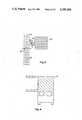
- FIG. 1is a top view of a section of an integrated circuit device of this invention with the link point set apart from the main conductive paths.
- FIG. 2is a cross-sectional view of FIG. 1 taken along line 2--2.
- FIG. 3is a top view of the first metal layer of the device of FIG. 1.
- FIG. 4is a top view of the link insulator of the device of FIG. 1.
- FIG. 5is a top view of the surface of the device of FIG. 1 lacking polyimide.
- FIG. 6is a top view of the second metal layer of the device of FIG. 1.
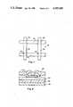
- FIG. 7is a top view of an integrated circuit device with the link point corresponding to the main conductive paths.
- FIG. 8is a cross-sectional view taken along line 8--8 of FIG. 7.
- the integrated circuit device 10 of this inventioncomprises a first metal layer 12, a link insulator layer 14 and a second metal layer 16 which is supported on a base oxide 18 and a substrate 20.
- the first metal layer 12is configured so that it includes a first main conductive path 22.
- the second metal layer 16includes a second main conductive path 24.
- the first main conductive path 22 and the second main conductive path 24provide means for electrically connecting the integrated circuit device of this invention to other electrical components into which the device is incorporated by any conventional means.
- a link point 26is comprised of a sandwich of the first metal 12, the link insulator 14 and the second metal 16.
- the link point 26is set apart from the first main conductive path 24 so that electrical connection between the first metal layer 12 and the second metal layer 16 can be effective without interrupting the main conductive paths 22 and 24.
- the first metal section 28 which forms part of the link point 26is electrically connected to the first main conductive path 22 by means of bridge 30 formed of the first metal.
- the second metal 16 which forms a part of the link point 26is electrically connected to the second main conductive path 24 by means of bridge 32 formed of the second metal.
- the polyimide layer 34can be formed on all sections of the integrated circuit device with the exception of the link point so that, at the link point, the second metal 16 directly contacts the link insulator material 14.
- the first metal layer 12 and the second metal layer 16can be formed of any electrically conducting metal or alloy capable of interacting with the link insulator layer to form an electrically conductive path including aluminum.
- Al-Si-Cu alloys or the like metals capable of forming silicides or the likemay be formed from insulating materials capable of being doped by mixing or alloying with the first metal 12 and the second metal 16 to form an electrically conductive path through the thickness of the link insulator layer 14.
- Suitable link insulator layersinclude amorphous germanium, amorphous silicon, undoped polysilicon, polycrystalline germanium or the like.
- a barrier layeris interposed between the link insulator layer 14 and each of the metal layers 12 and 16 in order to prevent diffusion of metal into the link insulator.
- Suitable diffusion barriersinclude silicon dioxide, silicon nitride, refractory nitrides such as tungsten nitride, titanium nitride or the like.
- Typical thicknesses for the diffusion barrier layeris between 0.1 ⁇ and 1 ⁇ which permits formation of the electrical path between the first and second metals and provides the diffusion barrier. It is preferred that the first and second metals comprise aluminum or its alloys and that the link insulator material comprise amorphous silicon.
- the electrically conductive path through the link insulator layer 14is formed by means of a low-power laser opening in the 0.2 ⁇ to 1 ⁇ range, such as an argon laser or the like, laser operating at a power between about 1 and about 3 watts, preferably between about 1 and about 1.5 watts for a light beam about 3 microns in diameter. For light beams having a smaller diameter, lower power lasers can be utilized to obtain equivalent power densities.
- the link pointis exposed to the laser for a period of time of between about 0.01 and about 10 milliseconds, preferably about 0.1 and about 1 milliseconds.
- the exposed second metal surface 16 of the link point 26is exposed to the laser to form a hole through the link insulator layer 14 while permitting alloying along the exposed surface of the hole, thereby connecting the first and second metals.
- the thickness of the link insulator materialshould be between about 0.2 ⁇ and about 2 ⁇ , preferably between about 0.5 ⁇ and 1 ⁇ while the first and second metal layers should have a thickness of between and 0.3 ⁇ and about 2 ⁇ , preferably between about 0.5 ⁇ and about 1 ⁇ .
- the base oxidetypically comprises silicon dioxide, and can have a thickness between about 0.4 ⁇ and about 2 ⁇ .
- the substratecan comprise crystalline silicon, GaAs, or silicon on insulator.
- Electrical connection to the link point 26 from the main conductive paths 22 and 24 through bridges 30 and/or 32can be cut by exposing the bridges 30 or 32 to a laser under the same condition set forth above for forming the link point.
- the bridges 30 and/or 32can be cut by the laser at cut points 36 and 38.
- the main conductive paths 22 and 24can be cut with a laser under these same conditions at cut points 40 and 42 when desired. Only one metal layer 12 or 16 is positioned at cut points 36, 38, 40 and 42. If more than one metal layer were present at the cut points 36, 38, 40 and 42, the undesirable possibility of electrically connecting the metal layers would be present.
- the integrated circuit device 48includes first main conductive paths 50 and second main conductive paths 52 and link points 54.
- Each link point 54includes the second metal layer 56, the insulator layer 58, the barrier diffusion layers 60 and 62, the first metal layer 64, the base oxide 66 and the substrate 68.
- the alloye.g., Al, Si, Cu is deposited by sputter typically to a thickness of about 0.5 ⁇ m.
- the waferthen is annealed at about 450° C. for about 10 minutes in forming gas.
- the metal surfacethen is spin cleaned in isopropyl alcohol.
- Silicon dioxide(10 nm ⁇ 2 nm) then is deposited by chemical vapor deposition at 425° C.
- the waferthen is spun cleaned in isopropyl alcohol.
- Amorphous silicon of 0.7 ⁇ mthen is deposited by sputter deposition.
- the amorphous silicon surfacethen is spin cleaned in isoproply alcohol.
- Silicon dioxide, e.g., 10 nm ⁇ 2 nmthen is deposited by chemical vapor deposition at 425° C.
- the waferthen is spin cleaned in isopropyl alcohol and about 0.7 ⁇ m of an Al, Si, Cu alloy is deposited by sputter deposition.
Landscapes
- Physics & Mathematics (AREA)
- Engineering & Computer Science (AREA)
- High Energy & Nuclear Physics (AREA)
- Optics & Photonics (AREA)
- Condensed Matter Physics & Semiconductors (AREA)
- General Physics & Mathematics (AREA)
- Manufacturing & Machinery (AREA)
- Computer Hardware Design (AREA)
- Microelectronics & Electronic Packaging (AREA)
- Power Engineering (AREA)
- Health & Medical Sciences (AREA)
- Toxicology (AREA)
- Electromagnetism (AREA)
- Internal Circuitry In Semiconductor Integrated Circuit Devices (AREA)
Abstract
Description
The Government has rights in this invention pursuant to Contract No. F19628-80-C-0002 awarded by the Department of the Air Force.
this is a division of application Ser. No. 328,356 filed Dec. 7, 1981 abandoned.
This invention relates to novel interconnect wiring arrangements on a silicon wafer and to methods for producing the same. More particularly, the present invention relates to methods for interconnecting a plurality of metal layers on a silicon wafer after transistors and wiring have been patterned and fabricated.
Prior to the present invention, metal layers each positioned on a different vertical height, separated by an insulating layer and positioned on a silicon wafer had been connected by means of relatively high power lasers such as dye lasers utilizing one or more pulses, each a few nanoseconds wide. The laser power is sufficiently high as to effect opening of the top metal layer, usually aluminum, removal of the intermediate silicon-containing layer by microexplosions and migration of metal into the opening through the insulating layer thickness to effect electrical contact between the metal layers. Typically, the laser power utilized is several kilowatts and the width of each pulse is between about 2 and 6 nanoseconds. The major problem with this prior technique for forming interconnections is that the high-powered laser causes microexplosions which, in turn, cause splatter of metal to occur. This results in poor control in forming electrically conductive paths in the desired pattern. In addition, this technique is generally unsuitable for cutting established conductive paths because of this metal splattering which many times creates new undesirable conductive paths.
It would be highly desirable to provide a means for interconnecting different metal layers positioned on a silicon wafer in a manner which provides relatively uniform conduction paths without the formation of new undesirable conductive paths. In addition, it would be desirable to provide such means which also is useful for cutting established conductive paths without creating new undesirable conductive paths.
The present invention provides an integrated circuit device which includes a plurality of metal layers with a link insulator layer interposed between the metal layers. The composition of the link insulator is capable of alloying with the metal in the metal layers to form a conductive path between the metal layers. A link point comprising the two metal layers and the link insulator layer can be set apart from a first main conductive path formed of the first metal and a second main conductive path formed of the second metal so that the metal layers in the link point can be interconnected or one or more of the metal layers in the link point can be electrically disconnected from the main conductive paths. Alternatively, the metal layers of the link point can each comprise the first main conductive path of the second main conductive. Interconnection of the metal layers in the link point is achieved by exposing the link point to a low power laser having a pulse in the order of about 1 millisecond. When utilizing these laser conditions, low resistivity connections can be achieved without damage to the base oxide, thereby avoiding exposure to the substrate.
FIG. 1 is a top view of a section of an integrated circuit device of this invention with the link point set apart from the main conductive paths.
FIG. 2 is a cross-sectional view of FIG. 1 taken alongline 2--2.
FIG. 3 is a top view of the first metal layer of the device of FIG. 1.
FIG. 4 is a top view of the link insulator of the device of FIG. 1.
FIG. 5 is a top view of the surface of the device of FIG. 1 lacking polyimide.
FIG. 6 is a top view of the second metal layer of the device of FIG. 1.
FIG. 7 is a top view of an integrated circuit device with the link point corresponding to the main conductive paths.
FIG. 8 is a cross-sectional view taken along line 8--8 of FIG. 7.
Referring to FIGS. 1 through 6, theintegrated circuit device 10 of this invention comprises afirst metal layer 12, alink insulator layer 14 and asecond metal layer 16 which is supported on abase oxide 18 and asubstrate 20. Thefirst metal layer 12 is configured so that it includes a first mainconductive path 22. Thesecond metal layer 16 includes a second mainconductive path 24. The first mainconductive path 22 and the second mainconductive path 24 provide means for electrically connecting the integrated circuit device of this invention to other electrical components into which the device is incorporated by any conventional means. Alink point 26 is comprised of a sandwich of thefirst metal 12, thelink insulator 14 and thesecond metal 16. Thelink point 26 is set apart from the first mainconductive path 24 so that electrical connection between thefirst metal layer 12 and thesecond metal layer 16 can be effective without interrupting the mainconductive paths first metal section 28 which forms part of thelink point 26 is electrically connected to the first mainconductive path 22 by means ofbridge 30 formed of the first metal. Similarly, thesecond metal 16 which forms a part of thelink point 26 is electrically connected to the second mainconductive path 24 by means ofbridge 32 formed of the second metal. Thepolyimide layer 34 can be formed on all sections of the integrated circuit device with the exception of the link point so that, at the link point, thesecond metal 16 directly contacts thelink insulator material 14.
Thefirst metal layer 12 and thesecond metal layer 16 can be formed of any electrically conducting metal or alloy capable of interacting with the link insulator layer to form an electrically conductive path including aluminum. Al-Si-Cu alloys or the like metals capable of forming silicides or the like may be formed from insulating materials capable of being doped by mixing or alloying with thefirst metal 12 and thesecond metal 16 to form an electrically conductive path through the thickness of thelink insulator layer 14. Suitable link insulator layers include amorphous germanium, amorphous silicon, undoped polysilicon, polycrystalline germanium or the like. A barrier layer is interposed between thelink insulator layer 14 and each of themetal layers link insulator layer 14 is formed by means of a low-power laser opening in the 0.2μ to 1μ range, such as an argon laser or the like, laser operating at a power between about 1 and about 3 watts, preferably between about 1 and about 1.5 watts for a light beam about 3 microns in diameter. For light beams having a smaller diameter, lower power lasers can be utilized to obtain equivalent power densities. The link point is exposed to the laser for a period of time of between about 0.01 and about 10 milliseconds, preferably about 0.1 and about 1 milliseconds. In forming the link point, the exposedsecond metal surface 16 of thelink point 26 is exposed to the laser to form a hole through thelink insulator layer 14 while permitting alloying along the exposed surface of the hole, thereby connecting the first and second metals. In order to achieve this desired electrical path, without disturbing thebase oxide 18, the thickness of the link insulator material should be between about 0.2μ and about 2μ, preferably between about 0.5μ and 1μ while the first and second metal layers should have a thickness of between and 0.3μ and about 2μ, preferably between about 0.5μ and about 1μ. The base oxide typically comprises silicon dioxide, and can have a thickness between about 0.4μ and about 2μ. The substrate can comprise crystalline silicon, GaAs, or silicon on insulator. Electrical connection to thelink point 26 from the mainconductive paths bridges 30 and/or 32 can be cut by exposing thebridges bridges 30 and/or 32 can be cut by the laser atcut points 36 and 38. In addition, the mainconductive paths cut points metal layer cut points cut points
Referring to FIGS. 7 and 8, theintegrated circuit device 48 includes first mainconductive paths 50 and second mainconductive paths 52 andlink points 54. Eachlink point 54 includes thesecond metal layer 56, theinsulator layer 58, thebarrier diffusion layers first metal layer 64, thebase oxide 66 and thesubstrate 68.
The alloy, e.g., Al, Si, Cu is deposited by sputter typically to a thickness of about 0.5 μm. The wafer then is annealed at about 450° C. for about 10 minutes in forming gas. The metal surface then is spin cleaned in isopropyl alcohol. Silicon dioxide (10 nm±2 nm) then is deposited by chemical vapor deposition at 425° C. The wafer then is spun cleaned in isopropyl alcohol. Amorphous silicon of 0.7 μm then is deposited by sputter deposition. The amorphous silicon surface then is spin cleaned in isoproply alcohol. Silicon dioxide, e.g., 10 nm±2 nm then is deposited by chemical vapor deposition at 425° C. The wafer then is spin cleaned in isopropyl alcohol and about 0.7 μm of an Al, Si, Cu alloy is deposited by sputter deposition.
Claims (3)
1. The process for forming an electrically conductive path between a first metal layer and a second metal layer in an integrated circuit device which comprises providing a substrate, a layer of base oxide on said substrate, a first metal layer on at least a portion of said base oxide having at least one first main conductive path, at least one first link point portion and at least one bridge portion extending between said first main conductive path and said link point portion, a layer of link insulator selected from the group consisting of amorphous germanium, amorphous silicon undoped polysilicon and polycrystalline germanium overlying at least said first link point portion, a second metal layer overlying said link insulator at a second link point portion at least in a region that also generally overlies said first link point portion to form a link point and including at least one second main conductive path and at least one bridge portion extending between said second means conductive path and said second link point, and an insulating metal diffusion barrier layer between said link insulator layer and each of said first metal layer and said second metal layer, and
exposing the second metal layer of said link point to a laser pulse between about one and about three watts for a time period between about 0.01 and about 10 milliseconds to effect alloying between the first metal, said second metal and the link insulator material.
2. The process of claim 1 wherin said time period is between about 0.1 and about 1 millisecond.
3. The process of claim 1 wherein said laser pulse is between about 1 amd 1.5 watts.
Priority Applications (1)
| Application Number | Priority Date | Filing Date | Title |
|---|---|---|---|
| US06/657,128US4585490A (en) | 1981-12-07 | 1984-10-03 | Method of making a conductive path in multi-layer metal structures by low power laser beam |
Applications Claiming Priority (2)
| Application Number | Priority Date | Filing Date | Title |
|---|---|---|---|
| US32835681A | 1981-12-07 | 1981-12-07 | |
| US06/657,128US4585490A (en) | 1981-12-07 | 1984-10-03 | Method of making a conductive path in multi-layer metal structures by low power laser beam |
Related Parent Applications (1)
| Application Number | Title | Priority Date | Filing Date |
|---|---|---|---|
| US32835681ADivision | 1981-12-07 | 1981-12-07 |
Publications (1)
| Publication Number | Publication Date |
|---|---|
| US4585490Atrue US4585490A (en) | 1986-04-29 |
Family
ID=26986339
Family Applications (1)
| Application Number | Title | Priority Date | Filing Date |
|---|---|---|---|
| US06/657,128Expired - Fee RelatedUS4585490A (en) | 1981-12-07 | 1984-10-03 | Method of making a conductive path in multi-layer metal structures by low power laser beam |
Country Status (1)
| Country | Link |
|---|---|
| US (1) | US4585490A (en) |
Cited By (68)
| Publication number | Priority date | Publication date | Assignee | Title |
|---|---|---|---|---|
| US4692190A (en)* | 1984-12-27 | 1987-09-08 | Kabushiki Kaisha Toshiba | Trimming of metal interconnection layer by selective migration of metal atoms by energy beams |
| US4708747A (en)* | 1986-10-16 | 1987-11-24 | Harris Corporation | Dielectric for laser trimming |
| US4723197A (en)* | 1985-12-16 | 1988-02-02 | National Semiconductor Corporation | Bonding pad interconnection structure |
| US4751197A (en)* | 1984-07-18 | 1988-06-14 | Texas Instruments Incorporated | Make-link programming of semiconductor devices using laser enhanced thermal breakdown of insulator |
| US4839711A (en)* | 1986-10-16 | 1989-06-13 | Harris Corporation | Dielectric for laser trimming |
| US4843034A (en)* | 1987-06-12 | 1989-06-27 | Massachusetts Institute Of Technology | Fabrication of interlayer conductive paths in integrated circuits |
| US4873201A (en)* | 1987-12-10 | 1989-10-10 | Minnesota Mining And Manufacturing Company | Method for fabricating an interconnected array of semiconductor devices |
| US4875971A (en)* | 1987-04-05 | 1989-10-24 | Elron Electronic Industries, Ltd. | Fabrication of customized integrated circuits |
| US4914055A (en)* | 1989-08-24 | 1990-04-03 | Advanced Micro Devices, Inc. | Semiconductor antifuse structure and method |
| US4924287A (en)* | 1985-01-20 | 1990-05-08 | Avner Pdahtzur | Personalizable CMOS gate array device and technique |
| US4960729A (en)* | 1987-03-10 | 1990-10-02 | Elron Electronic Industries Ltd. | Integrated circuits and a method for manufacture thereof |
| US4965655A (en)* | 1987-12-10 | 1990-10-23 | Minnesota Mining And Manufacturing Company | Interconnected semiconductor devices |
| US4968643A (en)* | 1986-08-12 | 1990-11-06 | Fujitsu Limited | Method for fabricating an activatable conducting link for metallic conductive wiring in a semiconductor device |
| US5155565A (en)* | 1988-02-05 | 1992-10-13 | Minnesota Mining And Manufacturing Company | Method for manufacturing an amorphous silicon thin film solar cell and Schottky diode on a common substrate |
| US5166556A (en)* | 1991-01-22 | 1992-11-24 | Myson Technology, Inc. | Programmable antifuse structure, process, logic cell and architecture for programmable integrated circuits |
| US5258643A (en)* | 1991-07-25 | 1993-11-02 | Massachusetts Institute Of Technology | Electrically programmable link structures and methods of making same |
| US5270251A (en)* | 1993-02-25 | 1993-12-14 | Massachusetts Institute Of Technology | Incoherent radiation regulated voltage programmable link |
| US5322812A (en)* | 1991-03-20 | 1994-06-21 | Crosspoint Solutions, Inc. | Improved method of fabricating antifuses in an integrated circuit device and resulting structure |
| US5485031A (en)* | 1993-11-22 | 1996-01-16 | Actel Corporation | Antifuse structure suitable for VLSI application |
| US5485032A (en)* | 1992-12-18 | 1996-01-16 | International Business Machines Corporation | Antifuse element with electrical or optical programming |
| US5537108A (en)* | 1994-02-08 | 1996-07-16 | Prolinx Labs Corporation | Method and structure for programming fuses |
| US5557137A (en)* | 1992-09-23 | 1996-09-17 | Massachusetts Institute Of Technology | Voltage programmable link having reduced capacitance |
| US5572409A (en)* | 1994-02-08 | 1996-11-05 | Prolinx Labs Corporation | Apparatus including a programmable socket adapter for coupling an electronic component to a component socket on a printed circuit board |
| US5614756A (en)* | 1990-04-12 | 1997-03-25 | Actel Corporation | Metal-to-metal antifuse with conductive |
| US5641703A (en)* | 1991-07-25 | 1997-06-24 | Massachusetts Institute Of Technology | Voltage programmable links for integrated circuits |
| US5726482A (en)* | 1994-02-08 | 1998-03-10 | Prolinx Labs Corporation | Device-under-test card for a burn-in board |
| US5767575A (en)* | 1995-10-17 | 1998-06-16 | Prolinx Labs Corporation | Ball grid array structure and method for packaging an integrated circuit chip |
| US5780323A (en)* | 1990-04-12 | 1998-07-14 | Actel Corporation | Fabrication method for metal-to-metal antifuses incorporating a tungsten via plug |
| US5808351A (en)* | 1994-02-08 | 1998-09-15 | Prolinx Labs Corporation | Programmable/reprogramable structure using fuses and antifuses |
| US5813881A (en)* | 1994-02-08 | 1998-09-29 | Prolinx Labs Corporation | Programmable cable and cable adapter using fuses and antifuses |
| US5834824A (en)* | 1994-02-08 | 1998-11-10 | Prolinx Labs Corporation | Use of conductive particles in a nonconductive body as an integrated circuit antifuse |
| US5872338A (en)* | 1996-04-10 | 1999-02-16 | Prolinx Labs Corporation | Multilayer board having insulating isolation rings |
| US5906043A (en)* | 1995-01-18 | 1999-05-25 | Prolinx Labs Corporation | Programmable/reprogrammable structure using fuses and antifuses |
| US5906042A (en)* | 1995-10-04 | 1999-05-25 | Prolinx Labs Corporation | Method and structure to interconnect traces of two conductive layers in a printed circuit board |
| US5917229A (en)* | 1994-02-08 | 1999-06-29 | Prolinx Labs Corporation | Programmable/reprogrammable printed circuit board using fuse and/or antifuse as interconnect |
| US5920789A (en)* | 1994-10-11 | 1999-07-06 | Massachusetts Institute Of Technology | Technique for producing interconnecting conductive links |
| US5932487A (en)* | 1998-03-12 | 1999-08-03 | Worldwide Semiconductor Manufacturing Corporation | Method for forming a planar intermetal dielectric layer |
| US5940727A (en)* | 1994-10-11 | 1999-08-17 | Massachusetts Institute Of Technology | Technique for producing interconnecting conductive links |
| US6034427A (en)* | 1998-01-28 | 2000-03-07 | Prolinx Labs Corporation | Ball grid array structure and method for packaging an integrated circuit chip |
| US6191486B1 (en) | 1994-03-10 | 2001-02-20 | Massachusetts Institute Of Technology | Technique for producing interconnecting conductive links |
| US6329272B1 (en) | 1999-06-14 | 2001-12-11 | Technologies Ltrim Inc. | Method and apparatus for iteratively, selectively tuning the impedance of integrated semiconductor devices using a focussed heating source |
| US6459032B1 (en) | 1995-05-15 | 2002-10-01 | Daniel Luch | Substrate structures for integrated series connected photovoltaic arrays and process of manufacture of such arrays |
| US20060180195A1 (en)* | 1999-03-30 | 2006-08-17 | Daniel Luch | Substrate and collector grid structures for integrated photovoltaic arrays and process of manufacture of such arrays |
| US20070117227A1 (en)* | 2005-11-23 | 2007-05-24 | Gsi Group Corporation | Method And System for Iteratively, Selectively Tuning A Parameter Of A Doped Workpiece Using A Pulsed Laser |
| US20070164320A1 (en)* | 2006-01-19 | 2007-07-19 | Technologies Ltrim Inc. | Tunable semiconductor component provided with a current barrier |
| US20080011350A1 (en)* | 1999-03-30 | 2008-01-17 | Daniel Luch | Collector grid, electrode structures and interconnect structures for photovoltaic arrays and other optoelectric devices |
| US20080227236A1 (en)* | 1995-05-15 | 2008-09-18 | Daniel Luch | Substrate structures for integrated series connected photovoltaic arrays and process of manufacture of such arrays |
| US20080314433A1 (en)* | 1995-05-15 | 2008-12-25 | Daniel Luch | Substrate structures for integrated series connected photovoltaic arrays and process of manufacture of such arrays |
| US7507903B2 (en) | 1999-03-30 | 2009-03-24 | Daniel Luch | Substrate and collector grid structures for integrated series connected photovoltaic arrays and process of manufacture of such arrays |
| US20090107538A1 (en)* | 2007-10-29 | 2009-04-30 | Daniel Luch | Collector grid and interconnect structures for photovoltaic arrays and modules |
| US20090111206A1 (en)* | 1999-03-30 | 2009-04-30 | Daniel Luch | Collector grid, electrode structures and interrconnect structures for photovoltaic arrays and methods of manufacture |
| US20100218824A1 (en)* | 2000-02-04 | 2010-09-02 | Daniel Luch | Substrate structures for integrated series connected photovoltaic arrays and process of manufacture of such arrays |
| US20100224230A1 (en)* | 2006-04-13 | 2010-09-09 | Daniel Luch | Collector grid and interconnect structures for photovoltaic arrays and modules |
| US20100229942A1 (en)* | 2000-02-04 | 2010-09-16 | Daniel Luch | Substrate structures for integrated series connected photovoltaic arrays and process of manufacture of such arrays |
| US20100269902A1 (en)* | 2006-04-13 | 2010-10-28 | Daniel Luch | Collector grid and interconnect structures for photovoltaic arrays and modules |
| US20110067754A1 (en)* | 2000-02-04 | 2011-03-24 | Daniel Luch | Substrate structures for integrated series connected photovoltaic arrays and process of manufacture of such arrays |
| US20110212344A1 (en)* | 2010-02-26 | 2011-09-01 | Qing Gong | Metalized Plastic Articles and Methods Thereof |
| US8198696B2 (en) | 2000-02-04 | 2012-06-12 | Daniel Luch | Substrate structures for integrated series connected photovoltaic arrays and process of manufacture of such arrays |
| US8222513B2 (en) | 2006-04-13 | 2012-07-17 | Daniel Luch | Collector grid, electrode structures and interconnect structures for photovoltaic arrays and methods of manufacture |
| US8664030B2 (en) | 1999-03-30 | 2014-03-04 | Daniel Luch | Collector grid and interconnect structures for photovoltaic arrays and modules |
| US8729385B2 (en) | 2006-04-13 | 2014-05-20 | Daniel Luch | Collector grid and interconnect structures for photovoltaic arrays and modules |
| US8822810B2 (en) | 2006-04-13 | 2014-09-02 | Daniel Luch | Collector grid and interconnect structures for photovoltaic arrays and modules |
| US8841000B2 (en) | 2010-08-19 | 2014-09-23 | Byd Company Limited | Metalized plastic articles and methods thereof |
| US8884155B2 (en) | 2006-04-13 | 2014-11-11 | Daniel Luch | Collector grid and interconnect structures for photovoltaic arrays and modules |
| US8920936B2 (en) | 2010-01-15 | 2014-12-30 | Byd Company Limited | Metalized plastic articles and methods thereof |
| US9006563B2 (en) | 2006-04-13 | 2015-04-14 | Solannex, Inc. | Collector grid and interconnect structures for photovoltaic arrays and modules |
| US9236512B2 (en) | 2006-04-13 | 2016-01-12 | Daniel Luch | Collector grid and interconnect structures for photovoltaic arrays and modules |
| US9865758B2 (en) | 2006-04-13 | 2018-01-09 | Daniel Luch | Collector grid and interconnect structures for photovoltaic arrays and modules |
Citations (26)
| Publication number | Priority date | Publication date | Assignee | Title |
|---|---|---|---|---|
| US3771026A (en)* | 1970-03-25 | 1973-11-06 | Hitachi Ltd | Conductive region for semiconductor device and method for making the same |
| US4023005A (en)* | 1975-04-21 | 1977-05-10 | Raytheon Company | Laser welding high reflectivity metals |
| CA1010156A (en)* | 1973-12-03 | 1977-05-10 | Nippon Electric Company | Multi-layer wiring structure |
| JPS52135865A (en)* | 1976-05-10 | 1977-11-14 | Tokyo Shibaura Electric Co | Method and device for forming branced pipe |
| JPS5326689A (en)* | 1976-08-25 | 1978-03-11 | Hitachi Ltd | Semiconductor integrated circuit unit |
| US4151545A (en)* | 1976-10-29 | 1979-04-24 | Robert Bosch Gmbh | Semiconductor electric circuit device with plural-layer aluminum base metallization |
| JPS5485122A (en)* | 1977-12-21 | 1979-07-06 | Nippon Steel Corp | Top pouring casting apparatus |
| US4168444A (en)* | 1976-08-19 | 1979-09-18 | U.S. Philips Corporation | Imaging devices |
| US4177474A (en)* | 1977-05-18 | 1979-12-04 | Energy Conversion Devices, Inc. | High temperature amorphous semiconductor member and method of making the same |
| US4190855A (en)* | 1976-08-11 | 1980-02-26 | Sharp Kabushiki Kaisha | Installation of a semiconductor chip on a glass substrate |
| US4270137A (en)* | 1977-12-15 | 1981-05-26 | U.S. Philips Corporation | Field-effect devices |
| US4270960A (en)* | 1978-10-23 | 1981-06-02 | U.S. Philips Corporation | Method of manufacturing a semiconductor device utilizing a mono-polycrystalline deposition on a predeposited amorphous layer |
| US4272775A (en)* | 1978-07-03 | 1981-06-09 | National Semiconductor Corporation | Laser trim protection process and structure |
| US4275410A (en)* | 1978-11-29 | 1981-06-23 | Hughes Aircraft Company | Three-dimensionally structured microelectronic device |
| US4289834A (en)* | 1977-10-20 | 1981-09-15 | Ibm Corporation | Dense dry etched multi-level metallurgy with non-overlapped vias |
| US4335362A (en)* | 1978-11-17 | 1982-06-15 | Institut Fur Angewandte Physik Der Universitat Bern | Semiconductor device and a method of contacting a partial region of a semiconductor surface |
| US4372989A (en)* | 1979-06-20 | 1983-02-08 | Siemens Aktiengesellschaft | Process for producing coarse-grain crystalline/mono-crystalline metal and alloy films |
| US4387503A (en)* | 1981-08-13 | 1983-06-14 | Mostek Corporation | Method for programming circuit elements in integrated circuits |
| US4398343A (en)* | 1980-05-26 | 1983-08-16 | Shunpei Yamazaki | Method of making semi-amorphous semiconductor device |
| US4413272A (en)* | 1979-09-05 | 1983-11-01 | Fujitsu Limited | Semiconductor devices having fuses |
| US4437109A (en)* | 1980-11-07 | 1984-03-13 | General Electric Company | Silicon-on-sapphire body with conductive paths therethrough |
| US4438450A (en)* | 1979-11-30 | 1984-03-20 | Bell Telephone Laboratories, Incorporated | Solid state device with conductors having chain-shaped grain structure |
| US4446613A (en)* | 1981-10-19 | 1984-05-08 | Intel Corporation | Integrated circuit resistor and method of fabrication |
| US4456490A (en)* | 1983-03-09 | 1984-06-26 | Westinghouse Electric Corp. | Laser annealing of MIS devices by back surface laser treatment |
| US4462150A (en)* | 1981-11-10 | 1984-07-31 | Tokyo Shibaura Denki Kabushiki Kaisha | Method of forming energy beam activated conductive regions between circuit elements |
| US4467312A (en)* | 1980-12-23 | 1984-08-21 | Tokyo Shibaura Denki Kabushiki Kaisha | Semiconductor resistor device |
- 1984
- 1984-10-03USUS06/657,128patent/US4585490A/ennot_activeExpired - Fee Related
Patent Citations (26)
| Publication number | Priority date | Publication date | Assignee | Title |
|---|---|---|---|---|
| US3771026A (en)* | 1970-03-25 | 1973-11-06 | Hitachi Ltd | Conductive region for semiconductor device and method for making the same |
| CA1010156A (en)* | 1973-12-03 | 1977-05-10 | Nippon Electric Company | Multi-layer wiring structure |
| US4023005A (en)* | 1975-04-21 | 1977-05-10 | Raytheon Company | Laser welding high reflectivity metals |
| JPS52135865A (en)* | 1976-05-10 | 1977-11-14 | Tokyo Shibaura Electric Co | Method and device for forming branced pipe |
| US4190855A (en)* | 1976-08-11 | 1980-02-26 | Sharp Kabushiki Kaisha | Installation of a semiconductor chip on a glass substrate |
| US4168444A (en)* | 1976-08-19 | 1979-09-18 | U.S. Philips Corporation | Imaging devices |
| JPS5326689A (en)* | 1976-08-25 | 1978-03-11 | Hitachi Ltd | Semiconductor integrated circuit unit |
| US4151545A (en)* | 1976-10-29 | 1979-04-24 | Robert Bosch Gmbh | Semiconductor electric circuit device with plural-layer aluminum base metallization |
| US4177474A (en)* | 1977-05-18 | 1979-12-04 | Energy Conversion Devices, Inc. | High temperature amorphous semiconductor member and method of making the same |
| US4289834A (en)* | 1977-10-20 | 1981-09-15 | Ibm Corporation | Dense dry etched multi-level metallurgy with non-overlapped vias |
| US4270137A (en)* | 1977-12-15 | 1981-05-26 | U.S. Philips Corporation | Field-effect devices |
| JPS5485122A (en)* | 1977-12-21 | 1979-07-06 | Nippon Steel Corp | Top pouring casting apparatus |
| US4272775A (en)* | 1978-07-03 | 1981-06-09 | National Semiconductor Corporation | Laser trim protection process and structure |
| US4270960A (en)* | 1978-10-23 | 1981-06-02 | U.S. Philips Corporation | Method of manufacturing a semiconductor device utilizing a mono-polycrystalline deposition on a predeposited amorphous layer |
| US4335362A (en)* | 1978-11-17 | 1982-06-15 | Institut Fur Angewandte Physik Der Universitat Bern | Semiconductor device and a method of contacting a partial region of a semiconductor surface |
| US4275410A (en)* | 1978-11-29 | 1981-06-23 | Hughes Aircraft Company | Three-dimensionally structured microelectronic device |
| US4372989A (en)* | 1979-06-20 | 1983-02-08 | Siemens Aktiengesellschaft | Process for producing coarse-grain crystalline/mono-crystalline metal and alloy films |
| US4413272A (en)* | 1979-09-05 | 1983-11-01 | Fujitsu Limited | Semiconductor devices having fuses |
| US4438450A (en)* | 1979-11-30 | 1984-03-20 | Bell Telephone Laboratories, Incorporated | Solid state device with conductors having chain-shaped grain structure |
| US4398343A (en)* | 1980-05-26 | 1983-08-16 | Shunpei Yamazaki | Method of making semi-amorphous semiconductor device |
| US4437109A (en)* | 1980-11-07 | 1984-03-13 | General Electric Company | Silicon-on-sapphire body with conductive paths therethrough |
| US4467312A (en)* | 1980-12-23 | 1984-08-21 | Tokyo Shibaura Denki Kabushiki Kaisha | Semiconductor resistor device |
| US4387503A (en)* | 1981-08-13 | 1983-06-14 | Mostek Corporation | Method for programming circuit elements in integrated circuits |
| US4446613A (en)* | 1981-10-19 | 1984-05-08 | Intel Corporation | Integrated circuit resistor and method of fabrication |
| US4462150A (en)* | 1981-11-10 | 1984-07-31 | Tokyo Shibaura Denki Kabushiki Kaisha | Method of forming energy beam activated conductive regions between circuit elements |
| US4456490A (en)* | 1983-03-09 | 1984-06-26 | Westinghouse Electric Corp. | Laser annealing of MIS devices by back surface laser treatment |
Non-Patent Citations (21)
| Title |
|---|
| Aggarwal, B. K., IBM TDB, 21 (1979) 3271.* |
| Aggarwal, B. K., IBM-TDB, 21 (1979) 3271. |
| Drowley et al. in Laser Solid Interactions . . . Materials Ed (J. Narayan et al.), North Holland, N.Y. 1982, p. 529.* |
| Drowley et al. in Laser-Solid Interactions . . . Materials Ed (J. Narayan et al.), North-Holland, N.Y. 1982, p. 529. |
| E. E. Conrad, "Aluminum-Copper-Silicon Semiconductor Metallurgy", IBM Technical Disclosure Bulletin, vol. 13 (1971), p. 3661. |
| E. E. Conrad, Aluminum Copper Silicon Semiconductor Metallurgy , IBM Technical Disclosure Bulletin, vol. 13 (1971), p. 3661.* |
| G. H. Chapman et al., "A Laser Linking Process for Restructurable VLSI*", MIT, CLEO '82, 4/14-16/82, Phoenix, Ariz. |
| G. H. Chapman et al., A Laser Linking Process for Restructurable VLSI* , MIT, CLEO 82, 4/14 16/82, Phoenix, Ariz.* |
| J. F. Smith et al., "Laser Induced Personalization & Alterations of LSI & VLSI Circuits", IBM Corporation. |
| J. F. Smith et al., Laser Induced Personalization & Alterations of LSI & VLSI Circuits , IBM Corporation.* |
| J. G. Posa, "Redundancy-What to do When the Bits go Out", 7/28/81, pp. 117-120, Electronics. |
| J. G. Posa, Redundancy What to do When the Bits go Out , 7/28/81, pp. 117 120, Electronics.* |
| J. I. Raffel et al., "Laser Programmed Vias for Restructurable VLSI*", pp. 132-135, Int'l Electron Devices Meeting, 12/1980. |
| J. I. Raffel et al., Laser Programmed Vias for Restructurable VLSI* , pp. 132 135, Int l Electron Devices Meeting, 12/1980.* |
| J. Leff, "Aluminum-Silicon Conductor Formation", IBM Technical Disclosure Bulletin, vol. 12 (1970), p. 1996. |
| J. Leff, Aluminum Silicon Conductor Formation , IBM Technical Disclosure Bulletin, vol. 12 (1970), p. 1996.* |
| J. M. Harris et al., "Solid-Phase Crystallization of Si Films in Contact with Al Layers", pp. 2897-2904, Journal of Applied Physics, V. 48, No. 7, Jul., 1977. |
| J. M. Harris et al., Solid Phase Crystallization of Si Films in Contact with Al Layers , pp. 2897 2904, Journal of Applied Physics, V. 48, No. 7, Jul., 1977.* |
| M. Hongo, et al., THD2 Connecting Conductors on Semiconductor Devices by Lasers Hitachi, Ltd. 4/15/82.* |
| O. Minato, et al., "A High-Speed Hi-CMOSII 4K Static RAM", pp. 449-453, IEEE Journal of Solid-State Circuits, v. SC-16, No. 5, Oct. 1981. |
| O. Minato, et al., A High Speed Hi CMOSII 4K Static RAM , pp. 449 453, IEEE Journal of Solid State Circuits, v. SC 16, No. 5, Oct. 1981.* |
Cited By (99)
| Publication number | Priority date | Publication date | Assignee | Title |
|---|---|---|---|---|
| US4751197A (en)* | 1984-07-18 | 1988-06-14 | Texas Instruments Incorporated | Make-link programming of semiconductor devices using laser enhanced thermal breakdown of insulator |
| US4692190A (en)* | 1984-12-27 | 1987-09-08 | Kabushiki Kaisha Toshiba | Trimming of metal interconnection layer by selective migration of metal atoms by energy beams |
| US4924287A (en)* | 1985-01-20 | 1990-05-08 | Avner Pdahtzur | Personalizable CMOS gate array device and technique |
| US4723197A (en)* | 1985-12-16 | 1988-02-02 | National Semiconductor Corporation | Bonding pad interconnection structure |
| US4968643A (en)* | 1986-08-12 | 1990-11-06 | Fujitsu Limited | Method for fabricating an activatable conducting link for metallic conductive wiring in a semiconductor device |
| US4839711A (en)* | 1986-10-16 | 1989-06-13 | Harris Corporation | Dielectric for laser trimming |
| US4708747A (en)* | 1986-10-16 | 1987-11-24 | Harris Corporation | Dielectric for laser trimming |
| US4960729A (en)* | 1987-03-10 | 1990-10-02 | Elron Electronic Industries Ltd. | Integrated circuits and a method for manufacture thereof |
| US4875971A (en)* | 1987-04-05 | 1989-10-24 | Elron Electronic Industries, Ltd. | Fabrication of customized integrated circuits |
| US4843034A (en)* | 1987-06-12 | 1989-06-27 | Massachusetts Institute Of Technology | Fabrication of interlayer conductive paths in integrated circuits |
| US4873201A (en)* | 1987-12-10 | 1989-10-10 | Minnesota Mining And Manufacturing Company | Method for fabricating an interconnected array of semiconductor devices |
| US4965655A (en)* | 1987-12-10 | 1990-10-23 | Minnesota Mining And Manufacturing Company | Interconnected semiconductor devices |
| US5155565A (en)* | 1988-02-05 | 1992-10-13 | Minnesota Mining And Manufacturing Company | Method for manufacturing an amorphous silicon thin film solar cell and Schottky diode on a common substrate |
| US4914055A (en)* | 1989-08-24 | 1990-04-03 | Advanced Micro Devices, Inc. | Semiconductor antifuse structure and method |
| EP0414361A3 (en)* | 1989-08-24 | 1991-09-18 | Advanced Micro Devices, Inc. | Semiconductor antifuse structure and method |
| US5780323A (en)* | 1990-04-12 | 1998-07-14 | Actel Corporation | Fabrication method for metal-to-metal antifuses incorporating a tungsten via plug |
| US5614756A (en)* | 1990-04-12 | 1997-03-25 | Actel Corporation | Metal-to-metal antifuse with conductive |
| US5763898A (en)* | 1990-04-12 | 1998-06-09 | Actel Corporation | Above via metal-to-metal antifuses incorporating a tungsten via plug |
| US5166556A (en)* | 1991-01-22 | 1992-11-24 | Myson Technology, Inc. | Programmable antifuse structure, process, logic cell and architecture for programmable integrated circuits |
| US5322812A (en)* | 1991-03-20 | 1994-06-21 | Crosspoint Solutions, Inc. | Improved method of fabricating antifuses in an integrated circuit device and resulting structure |
| US5258643A (en)* | 1991-07-25 | 1993-11-02 | Massachusetts Institute Of Technology | Electrically programmable link structures and methods of making same |
| US5304508A (en)* | 1991-07-25 | 1994-04-19 | Massachusetts Institute Of Technology | Method of making electrically programmable link structures |
| US5641703A (en)* | 1991-07-25 | 1997-06-24 | Massachusetts Institute Of Technology | Voltage programmable links for integrated circuits |
| US5557137A (en)* | 1992-09-23 | 1996-09-17 | Massachusetts Institute Of Technology | Voltage programmable link having reduced capacitance |
| US5485032A (en)* | 1992-12-18 | 1996-01-16 | International Business Machines Corporation | Antifuse element with electrical or optical programming |
| US5270251A (en)* | 1993-02-25 | 1993-12-14 | Massachusetts Institute Of Technology | Incoherent radiation regulated voltage programmable link |
| US5485031A (en)* | 1993-11-22 | 1996-01-16 | Actel Corporation | Antifuse structure suitable for VLSI application |
| US6111302A (en)* | 1993-11-22 | 2000-08-29 | Actel Corporation | Antifuse structure suitable for VLSI application |
| US5572409A (en)* | 1994-02-08 | 1996-11-05 | Prolinx Labs Corporation | Apparatus including a programmable socket adapter for coupling an electronic component to a component socket on a printed circuit board |
| US5726482A (en)* | 1994-02-08 | 1998-03-10 | Prolinx Labs Corporation | Device-under-test card for a burn-in board |
| US5813881A (en)* | 1994-02-08 | 1998-09-29 | Prolinx Labs Corporation | Programmable cable and cable adapter using fuses and antifuses |
| US5808351A (en)* | 1994-02-08 | 1998-09-15 | Prolinx Labs Corporation | Programmable/reprogramable structure using fuses and antifuses |
| US5917229A (en)* | 1994-02-08 | 1999-06-29 | Prolinx Labs Corporation | Programmable/reprogrammable printed circuit board using fuse and/or antifuse as interconnect |
| US5834824A (en)* | 1994-02-08 | 1998-11-10 | Prolinx Labs Corporation | Use of conductive particles in a nonconductive body as an integrated circuit antifuse |
| US5537108A (en)* | 1994-02-08 | 1996-07-16 | Prolinx Labs Corporation | Method and structure for programming fuses |
| US6541868B2 (en) | 1994-03-10 | 2003-04-01 | Massachusetts Institute Of Technology | Interconnecting conductive links |
| US6191486B1 (en) | 1994-03-10 | 2001-02-20 | Massachusetts Institute Of Technology | Technique for producing interconnecting conductive links |
| US5920789A (en)* | 1994-10-11 | 1999-07-06 | Massachusetts Institute Of Technology | Technique for producing interconnecting conductive links |
| US5940727A (en)* | 1994-10-11 | 1999-08-17 | Massachusetts Institute Of Technology | Technique for producing interconnecting conductive links |
| US5906043A (en)* | 1995-01-18 | 1999-05-25 | Prolinx Labs Corporation | Programmable/reprogrammable structure using fuses and antifuses |
| US5962815A (en)* | 1995-01-18 | 1999-10-05 | Prolinx Labs Corporation | Antifuse interconnect between two conducting layers of a printed circuit board |
| US6459032B1 (en) | 1995-05-15 | 2002-10-01 | Daniel Luch | Substrate structures for integrated series connected photovoltaic arrays and process of manufacture of such arrays |
| US20080227236A1 (en)* | 1995-05-15 | 2008-09-18 | Daniel Luch | Substrate structures for integrated series connected photovoltaic arrays and process of manufacture of such arrays |
| US7732243B2 (en) | 1995-05-15 | 2010-06-08 | Daniel Luch | Substrate structures for integrated series connected photovoltaic arrays and process of manufacture of such arrays |
| US20080314433A1 (en)* | 1995-05-15 | 2008-12-25 | Daniel Luch | Substrate structures for integrated series connected photovoltaic arrays and process of manufacture of such arrays |
| US5906042A (en)* | 1995-10-04 | 1999-05-25 | Prolinx Labs Corporation | Method and structure to interconnect traces of two conductive layers in a printed circuit board |
| US5767575A (en)* | 1995-10-17 | 1998-06-16 | Prolinx Labs Corporation | Ball grid array structure and method for packaging an integrated circuit chip |
| US5987744A (en)* | 1996-04-10 | 1999-11-23 | Prolinx Labs Corporation | Method for supporting one or more electronic components |
| US5872338A (en)* | 1996-04-10 | 1999-02-16 | Prolinx Labs Corporation | Multilayer board having insulating isolation rings |
| US6034427A (en)* | 1998-01-28 | 2000-03-07 | Prolinx Labs Corporation | Ball grid array structure and method for packaging an integrated circuit chip |
| US5932487A (en)* | 1998-03-12 | 1999-08-03 | Worldwide Semiconductor Manufacturing Corporation | Method for forming a planar intermetal dielectric layer |
| CN1093688C (en)* | 1998-03-12 | 2002-10-30 | 台湾积体电路制造股份有限公司 | Fabrication method of via window |
| US8319097B2 (en) | 1999-03-30 | 2012-11-27 | Daniel Luch | Substrate and collector grid structures for integrated series connected photovoltaic arrays and process of manufacture of such arrays |
| US8110737B2 (en) | 1999-03-30 | 2012-02-07 | Daniel Luch | Collector grid, electrode structures and interrconnect structures for photovoltaic arrays and methods of manufacture |
| US8664030B2 (en) | 1999-03-30 | 2014-03-04 | Daniel Luch | Collector grid and interconnect structures for photovoltaic arrays and modules |
| US7868249B2 (en) | 1999-03-30 | 2011-01-11 | Daniel Luch | Substrate and collector grid structures for integrated series connected photovoltaic arrays and process of manufacture of such arrays |
| US7507903B2 (en) | 1999-03-30 | 2009-03-24 | Daniel Luch | Substrate and collector grid structures for integrated series connected photovoltaic arrays and process of manufacture of such arrays |
| US8304646B2 (en) | 1999-03-30 | 2012-11-06 | Daniel Luch | Substrate and collector grid structures for integrated series connected photovoltaic arrays and process of manufacture of such arrays |
| US20090111206A1 (en)* | 1999-03-30 | 2009-04-30 | Daniel Luch | Collector grid, electrode structures and interrconnect structures for photovoltaic arrays and methods of manufacture |
| US20090145551A1 (en)* | 1999-03-30 | 2009-06-11 | Daniel Luch | Substrate and collector grid structures for integrated series connected photovoltaic arrays and process of manufacture of such arrays |
| US20090173374A1 (en)* | 1999-03-30 | 2009-07-09 | Daniel Luch | Substrate and collector grid structures for integrated series connected photovoltaic arrays and process of manufacture of such arrays |
| US20110056537A1 (en)* | 1999-03-30 | 2011-03-10 | Daniel Luch | Substrate and collector grid structures for integrated series connected photovoltaic arrays and process of manufacturing of such arrays |
| US7635810B2 (en) | 1999-03-30 | 2009-12-22 | Daniel Luch | Substrate and collector grid structures for integrated photovoltaic arrays and process of manufacture of such arrays |
| US20060180195A1 (en)* | 1999-03-30 | 2006-08-17 | Daniel Luch | Substrate and collector grid structures for integrated photovoltaic arrays and process of manufacture of such arrays |
| US20080011350A1 (en)* | 1999-03-30 | 2008-01-17 | Daniel Luch | Collector grid, electrode structures and interconnect structures for photovoltaic arrays and other optoelectric devices |
| US7989692B2 (en) | 1999-03-30 | 2011-08-02 | Daniel Luch | Substrate and collector grid structures for integrated series connected photovoltaic arrays and process of manufacturing of such arrays |
| US7989693B2 (en) | 1999-03-30 | 2011-08-02 | Daniel Luch | Substrate and collector grid structures for integrated series connected photovoltaic arrays and process of manufacture of such arrays |
| US20110070678A1 (en)* | 1999-03-30 | 2011-03-24 | Daniel Luch | Substrate and collector grid structures for integrated series connected photovoltaic arrays and process of manufacture of such arrays |
| US7851700B2 (en) | 1999-03-30 | 2010-12-14 | Daniel Luch | Substrate and collector grid structures for integrated series connected photovoltaic arrays and process of manufacture of such arrays |
| US6329272B1 (en) | 1999-06-14 | 2001-12-11 | Technologies Ltrim Inc. | Method and apparatus for iteratively, selectively tuning the impedance of integrated semiconductor devices using a focussed heating source |
| US20100218824A1 (en)* | 2000-02-04 | 2010-09-02 | Daniel Luch | Substrate structures for integrated series connected photovoltaic arrays and process of manufacture of such arrays |
| US7898053B2 (en) | 2000-02-04 | 2011-03-01 | Daniel Luch | Substrate structures for integrated series connected photovoltaic arrays and process of manufacture of such arrays |
| US20110067754A1 (en)* | 2000-02-04 | 2011-03-24 | Daniel Luch | Substrate structures for integrated series connected photovoltaic arrays and process of manufacture of such arrays |
| US20100229942A1 (en)* | 2000-02-04 | 2010-09-16 | Daniel Luch | Substrate structures for integrated series connected photovoltaic arrays and process of manufacture of such arrays |
| US8198696B2 (en) | 2000-02-04 | 2012-06-12 | Daniel Luch | Substrate structures for integrated series connected photovoltaic arrays and process of manufacture of such arrays |
| US7898054B2 (en) | 2000-02-04 | 2011-03-01 | Daniel Luch | Substrate structures for integrated series connected photovoltaic arrays and process of manufacture of such arrays |
| US20070117227A1 (en)* | 2005-11-23 | 2007-05-24 | Gsi Group Corporation | Method And System for Iteratively, Selectively Tuning A Parameter Of A Doped Workpiece Using A Pulsed Laser |
| US7564078B2 (en) | 2006-01-19 | 2009-07-21 | Cadeka Microcircuits, Llc | Tunable semiconductor component provided with a current barrier |
| US20070164320A1 (en)* | 2006-01-19 | 2007-07-19 | Technologies Ltrim Inc. | Tunable semiconductor component provided with a current barrier |
| US8076568B2 (en) | 2006-04-13 | 2011-12-13 | Daniel Luch | Collector grid and interconnect structures for photovoltaic arrays and modules |
| US9006563B2 (en) | 2006-04-13 | 2015-04-14 | Solannex, Inc. | Collector grid and interconnect structures for photovoltaic arrays and modules |
| US9865758B2 (en) | 2006-04-13 | 2018-01-09 | Daniel Luch | Collector grid and interconnect structures for photovoltaic arrays and modules |
| US8222513B2 (en) | 2006-04-13 | 2012-07-17 | Daniel Luch | Collector grid, electrode structures and interconnect structures for photovoltaic arrays and methods of manufacture |
| US9236512B2 (en) | 2006-04-13 | 2016-01-12 | Daniel Luch | Collector grid and interconnect structures for photovoltaic arrays and modules |
| US20100224230A1 (en)* | 2006-04-13 | 2010-09-09 | Daniel Luch | Collector grid and interconnect structures for photovoltaic arrays and modules |
| US20100269902A1 (en)* | 2006-04-13 | 2010-10-28 | Daniel Luch | Collector grid and interconnect structures for photovoltaic arrays and modules |
| US8729385B2 (en) | 2006-04-13 | 2014-05-20 | Daniel Luch | Collector grid and interconnect structures for photovoltaic arrays and modules |
| US8822810B2 (en) | 2006-04-13 | 2014-09-02 | Daniel Luch | Collector grid and interconnect structures for photovoltaic arrays and modules |
| US8138413B2 (en) | 2006-04-13 | 2012-03-20 | Daniel Luch | Collector grid and interconnect structures for photovoltaic arrays and modules |
| US8884155B2 (en) | 2006-04-13 | 2014-11-11 | Daniel Luch | Collector grid and interconnect structures for photovoltaic arrays and modules |
| US20090107538A1 (en)* | 2007-10-29 | 2009-04-30 | Daniel Luch | Collector grid and interconnect structures for photovoltaic arrays and modules |
| US8920936B2 (en) | 2010-01-15 | 2014-12-30 | Byd Company Limited | Metalized plastic articles and methods thereof |
| US9435035B2 (en) | 2010-01-15 | 2016-09-06 | Byd Company Limited | Metalized plastic articles and methods thereof |
| US10392708B2 (en) | 2010-01-15 | 2019-08-27 | Byd Company Limited | Metalized plastic articles and methods thereof |
| US9103020B2 (en) | 2010-02-26 | 2015-08-11 | Byd Company Limited | Metalized plastic articles and methods thereof |
| US20110212344A1 (en)* | 2010-02-26 | 2011-09-01 | Qing Gong | Metalized Plastic Articles and Methods Thereof |
| US8846151B2 (en) | 2010-08-19 | 2014-09-30 | Byd Company Limited | Metalized plastic articles and methods thereof |
| US8841000B2 (en) | 2010-08-19 | 2014-09-23 | Byd Company Limited | Metalized plastic articles and methods thereof |
| US9770887B2 (en) | 2010-08-19 | 2017-09-26 | Byd Company Limited | Metalized plastic articles and methods thereof |
Similar Documents
| Publication | Publication Date | Title |
|---|---|---|
| US4585490A (en) | Method of making a conductive path in multi-layer metal structures by low power laser beam | |
| US4810663A (en) | Method of forming conductive path by low power laser pulse | |
| US4448636A (en) | Laser assisted lift-off | |
| US5663590A (en) | Product of process for formation of vias (or contact openings) and fuses in the same insulation layer with minimal additional steps | |
| US4561906A (en) | Laser activated polysilicon connections for redundancy | |
| US5380678A (en) | Bilayer barrier metal method for obtaining 100% step-coverage in contact vias without junction degradation | |
| US4916809A (en) | Method for programmable laser connection of two superimposed conductors of the interconnect system of an integrated circuit | |
| US4843034A (en) | Fabrication of interlayer conductive paths in integrated circuits | |
| US5244828A (en) | Method of fabricating a quantum device | |
| US4960729A (en) | Integrated circuits and a method for manufacture thereof | |
| JPH10270566A (en) | Solid circuit having laser fusing conductor and its manufacture | |
| US4968643A (en) | Method for fabricating an activatable conducting link for metallic conductive wiring in a semiconductor device | |
| US6191486B1 (en) | Technique for producing interconnecting conductive links | |
| US5288664A (en) | Method of forming wiring of semiconductor device | |
| JPH04229618A (en) | Contacts of integrated circuit devices and methods of forming them | |
| US5557137A (en) | Voltage programmable link having reduced capacitance | |
| EP0189598B1 (en) | Method for manufacturing a semiconductor device | |
| US5308794A (en) | Aluminum-germanium alloys for VLSI metallization | |
| US4673592A (en) | Metal planarization process | |
| US5861325A (en) | Technique for producing interconnecting conductive links | |
| US5920789A (en) | Technique for producing interconnecting conductive links | |
| US5940727A (en) | Technique for producing interconnecting conductive links | |
| EP0415526A2 (en) | Semiconductor device having wiring layers | |
| JPS63174336A (en) | Method for forming a dispersion barrier layer in contacts between multilayer interconnects | |
| JPS61174767A (en) | semiconductor device electrode |
Legal Events
| Date | Code | Title | Description |
|---|---|---|---|
| FEPP | Fee payment procedure | Free format text:PAYOR NUMBER ASSIGNED (ORIGINAL EVENT CODE: ASPN); ENTITY STATUS OF PATENT OWNER: LARGE ENTITY | |
| FEPP | Fee payment procedure | Free format text:PAT HLDR NO LONGER CLAIMS SMALL ENT STAT AS INDIV INVENTOR (ORIGINAL EVENT CODE: LSM1); ENTITY STATUS OF PATENT OWNER: LARGE ENTITY | |
| FPAY | Fee payment | Year of fee payment:4 | |
| REMI | Maintenance fee reminder mailed | ||
| REMI | Maintenance fee reminder mailed | ||
| LAPS | Lapse for failure to pay maintenance fees | ||
| FP | Lapsed due to failure to pay maintenance fee | Effective date:19940501 | |
| STCH | Information on status: patent discontinuation | Free format text:PATENT EXPIRED DUE TO NONPAYMENT OF MAINTENANCE FEES UNDER 37 CFR 1.362 |