US4583111A - Integrated circuit chip wiring arrangement providing reduced circuit inductance and controlled voltage gradients - Google Patents
Integrated circuit chip wiring arrangement providing reduced circuit inductance and controlled voltage gradientsDownload PDFInfo
- Publication number
- US4583111A US4583111AUS06/530,636US53063683AUS4583111AUS 4583111 AUS4583111 AUS 4583111AUS 53063683 AUS53063683 AUS 53063683AUS 4583111 AUS4583111 AUS 4583111A
- Authority
- US
- United States
- Prior art keywords
- bus
- gates
- chip
- current
- busses
- Prior art date
- Legal status (The legal status is an assumption and is not a legal conclusion. Google has not performed a legal analysis and makes no representation as to the accuracy of the status listed.)
- Expired - Lifetime
Links
- 239000004020conductorSubstances0.000claimsdescription37
- 230000001965increasing effectEffects0.000claimsdescription7
- 238000000034methodMethods0.000claimsdescription7
- 230000007423decreaseEffects0.000claimsdescription6
- 230000001939inductive effectEffects0.000claimsdescription6
- 230000000295complement effectEffects0.000claimsdescription3
- 230000003467diminishing effectEffects0.000claims3
- 238000009826distributionMethods0.000abstractdescription3
- 230000009467reductionEffects0.000abstractdescription3
- 230000003292diminished effectEffects0.000abstractdescription2
- 238000002955isolationMethods0.000abstractdescription2
- 230000008859changeEffects0.000description13
- 230000015654memoryEffects0.000description13
- 238000013461designMethods0.000description11
- VYPSYNLAJGMNEJ-UHFFFAOYSA-NSilicium dioxideChemical compoundO=[Si]=OVYPSYNLAJGMNEJ-UHFFFAOYSA-N0.000description8
- 238000009792diffusion processMethods0.000description7
- 230000004048modificationEffects0.000description7
- 238000012986modificationMethods0.000description7
- 238000005516engineering processMethods0.000description6
- 238000010586diagramMethods0.000description5
- 230000000694effectsEffects0.000description4
- 239000002184metalSubstances0.000description4
- 235000012239silicon dioxideNutrition0.000description4
- 239000000377silicon dioxideSubstances0.000description4
- 239000000758substrateSubstances0.000description4
- 238000013459approachMethods0.000description3
- 230000008901benefitEffects0.000description2
- 238000011960computer-aided designMethods0.000description2
- 230000001276controlling effectEffects0.000description2
- 230000003247decreasing effectEffects0.000description2
- 230000001419dependent effectEffects0.000description2
- 238000009413insulationMethods0.000description2
- 239000000463materialSubstances0.000description2
- 238000001465metallisationMethods0.000description2
- 230000001105regulatory effectEffects0.000description2
- 230000011664signalingEffects0.000description2
- 230000009471actionEffects0.000description1
- 230000002411adverseEffects0.000description1
- 238000010276constructionMethods0.000description1
- 230000004907fluxEffects0.000description1
- 238000002347injectionMethods0.000description1
- 239000007924injectionSubstances0.000description1
- 239000011810insulating materialSubstances0.000description1
- 239000012212insulatorSubstances0.000description1
- 230000010354integrationEffects0.000description1
- 238000004519manufacturing processMethods0.000description1
- 238000004377microelectronicMethods0.000description1
- 238000012856packingMethods0.000description1
- 230000035699permeabilityEffects0.000description1
- 230000008569processEffects0.000description1
- 238000000926separation methodMethods0.000description1
- 238000009827uniform distributionMethods0.000description1
Images


Classifications
- H—ELECTRICITY
- H01—ELECTRIC ELEMENTS
- H01L—SEMICONDUCTOR DEVICES NOT COVERED BY CLASS H10
- H01L23/00—Details of semiconductor or other solid state devices
- H01L23/52—Arrangements for conducting electric current within the device in operation from one component to another, i.e. interconnections, e.g. wires, lead frames
- H01L23/522—Arrangements for conducting electric current within the device in operation from one component to another, i.e. interconnections, e.g. wires, lead frames including external interconnections consisting of a multilayer structure of conductive and insulating layers inseparably formed on the semiconductor body
- H01L23/528—Layout of the interconnection structure
- H—ELECTRICITY
- H10—SEMICONDUCTOR DEVICES; ELECTRIC SOLID-STATE DEVICES NOT OTHERWISE PROVIDED FOR
- H10B—ELECTRONIC MEMORY DEVICES
- H10B20/00—Read-only memory [ROM] devices
- H—ELECTRICITY
- H01—ELECTRIC ELEMENTS
- H01L—SEMICONDUCTOR DEVICES NOT COVERED BY CLASS H10
- H01L2924/00—Indexing scheme for arrangements or methods for connecting or disconnecting semiconductor or solid-state bodies as covered by H01L24/00
- H01L2924/0001—Technical content checked by a classifier
- H01L2924/0002—Not covered by any one of groups H01L24/00, H01L24/00 and H01L2224/00
Definitions
- the present inventionis directed to large scale integrated circuit chips, and more particularly to wiring arrangements for such chips that reduce inductive crosstalk which might lead to signalling errors on the chip and provide for more uniform voltage distribution to the gates on the chip.
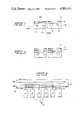
- an integrated circuit chip 10can comprise a multiplicity of logic gates 12 which are each connected in parallel with one another between a power bus 14 and a ground bus 16. As depicted in FIG.
- the logic gates 12are divided into two rows and the power and ground busses are also divided into two parallel conductive runs, that are respectively connected to the two rows.
- the chipmight have only one row of logic gates or a multiplicity of rows each being supplied by a separate conductive run.
- the particular number of rows of parallel connected logic gateswill be determined by the circuit to be incorporated in the chip and the design layout principles that are utilized.
- the chip of FIG. 1embodies a conventional wiring arrangement for supplying current to, and sinking it from, the individual logic gates. More particularly, the power supply bus 14 is connected to a bonding pad 18 that is disposed at one corner of the chip. This pad is in turn connected to one of the pins in the chip package which is supplied with current from a suitable supply source.
- the ground bus 16is similarly connected to a bonding pad 20 located on the diagonally opposite corner of the chip from the pad 18.
- the pad 20is connected to a suitable ground reference potential through a connecting pin on the chip package.
- the current supply pad 18can be located closer to the center of the top edge of the chip, and the current sinking pad can be located closer to the center of the bottom edge of the chip, rather than the pads being disposed on diagonally opposite corners.
- the currentflows from the bonding pad 18 through the various logic gates which are in a conductive state to the ground bus 16 and the bonding pad 20.
- the return path for the currentis from the bonding pad 20 back to the pad 18 which are separated by at least the length of the diagonal dimension of the chip package.
- This current flow pathis schematically indicated by the dashed lines in FIG. 1 for the case when one of the gates in the upper row of logic gates is conducting.
- Each gate which is at a conductive statewill also establish a similar flow path.
- this return pathis formed by the conductive runs on a printed circuit board (not shown) on which the chip is mounted. These runs lead from the connecting pins associated with the bonding pads 18 and 20 to edge connectors on the board which are hooked up to the power supply.
- the area that is encompassed by the current loopcomprises, at a minimum, a substantial portion of the area of the integrated circuit chip.
- the change in switching states of the logic gates on the chipmight be substantial enough to cause a significant change in the amount of current flowing from the pad 18 to the pad 20, and the current induced in other on-chip conductors by the changing magnetic field could be substantial enough to generate logic errors.
- a number of gatescan successively change states. A switching which occurs in a later stage of the series of gates can inductively trigger a change in state in an earlier stage during the same clock cycle, thus generating a logic error.
- the inductance L generated by a current loopcan be defined as follows: ##EQU1## where: ⁇ o is the effective permeability of the region on the chip in which the associated magnetic field is present,
- Ais the area circumscribed by the current loop
- Ris the mean radius of the loop.
- the area circumscribed by the current path on the chipis reduced by changing the conventional location of the bonding pads through which the current source and current sink are respectively connected to the logic gates. These pads are disposed physically adjacent to one another in accordance with the invention, rather than on opposite sides of the chip, for example.
- a further reduction in the area of the current loopis obtained by locating power and ground busses adjacent to one another relative to the logic gates. Ideally, these two busses can be superposed one over the other on different metallic layers of the chip, so that the space between them is only the thickness of the isolation layer which separates the two metallic layers.
- the voltage gradient across the gates on the chipis regulated to be the same for each gate by ensuring that the total length of the current path is the same for current flowing through each gate, and by varying the cross-sectional area of the power and ground busses in accordance with the magnitude of the current carried in each portion of the conductors.
- FIG. 1is a schematic and block diagram of a prior art wiring arrangement for an integrated circuit chip
- FIG. 2is a schematic and block diagram illustrating a first embodiment of a wiring arrangement for an integrated circuit chip incorporating the present invention
- FIG. 3is a schematic and block diagram of a modification of the wiring arrangement illustrated in FIG. 2;
- FIG. 4is a second embodiment of a wiring arrangement according to the present invention.
- FIG. 5is a top view of a portion of an integrated circuit (IC) chip implementing some of the principles of the present invention
- FIG. 6is an equivalent schematic electrical diagram of the circuit illustrated in FIG. 5;
- FIG. 7is a cross-sectional side view of the IC chip illustrated in FIG. 5, taken along the section line 7--7;
- FIG. 8is a sectional side view of an alternative embodiment of the construction of the chip illustrated in FIG. 5;
- FIG. 9is a diagram of a wiring arrangement showing design considerations for controlling the voltage gradient across the gates.
- one facet of the present inventionis concerned with alleviating the potentially error-producing noise that can be inductively generated during a switching cycle that produces a net change in current flow on the integrated circuit chip.
- a reduction of the area of the current loop on the chipis accomplished, in one aspect of the invention, by bringing the location of the current sinking pad 20 closer to that of the current supply pad 18 on the chip.
- An implementation of this principleis illustrated in FIG. 2.
- the wiring topology of the chipis generally similar to that illustrated in FIG. 1 except for the physical location of the bonding pad 20. In this instance, it is located physically adjacent to pad 18.
- the effect of the changeis to bring the source and sinking current paths closer together to thereby reduce the area between them.
- the area on the chip that is encompassed by the current loopis substantially reduced, as shown by the dashed line.
- the term "physically adjacent"does not necessarily imply that the bonding pads 18 and 20 are two pads which are next to each other on the chip. Rather, it is interpreted in a somewhat broader sense to refer to the location of the two pads relative to the logic gates.
- the most preferred implementation of this aspect of the inventionis to have the current supply and current sinking pads be successive pads on the same side of the chip, in practice certain design limitations may require that the source and ground pins be separated by at least one other pin. Under such circumstances the present invention would provide that the bonding pads be located as close as practically possible to one another and on the same side of the chip relative to the placement of the logic gates, even though they are not next to one another.
- FIG. 3A modification of this first feature of the invention is illustrated in FIG. 3.
- the bonding pad 18 for the power sourceis disposed at approximately the middle of one edge of the chip.
- the ground bus 16is connected at opposite ends thereof to two bonding pads 20 and 21. These pads are respectively disposed on opposite sides of the power source pad 18.
- the advantage of this layoutis that it balances the current flow paths on the chip. In other words, the magnetic field generated as a result of the flow of current in one of the paths illustrated by the dashed lines will diminish the effect of the magnetic field generated by the flow of current in the other illustrated path, since current flows in opposite directions in the two loops.
- ground bus 16could be connected to a single pad and the power bus connected to two pads respectively disposed on opposite sides of the grounded pad, to achieve the same effect.
- the power and ground busses 14 and 16are respectively located on opposite sides of the logic gates. This separation by the width of the gates results in a spacing between the supply and sink busses that accounts for a substantial portion of the reduced area encompassed by the current loop.
- FIGS. 2 and 3offers a significant decrease in current loop area over the conventional practice depicted in FIG. 1, additional modifications can be made to further decrease the inductance of the circuit.
- FIG. 4An embodiment which accomplishes this latter objective is illustrated in FIG. 4.
- further modification from conventional practiceresides in the placement of both current busses on the same side of the logic gates, so that they run adjacent to one another. With this embodiment, it can be seen that the area encompassed by the individual current loops is further decreased.
- the inductance of the circuitis likewise reduced, and is therefore less likely to result in the generation of logic errors.
- the area encompassed by the current loopsis at a minimum.
- minimization of the current loop areamay not be possible without adversely affecting other parameters.
- a practical implementation of the inventive conceptis to reduce the area of the current loop to the extent possible without seriously compromising other design considerations.
- FIG. 5A more detailed illustration of an integrated circuit chip implementing some of the principles of the invention is illustrated in FIG. 5.
- the circuit incorporated in the chip of FIG. 5is an MOS memory circuit, e.g., a ROM, such as that schematically illustrated in FIG. 6.
- the MOS memory circuitis used here to illustrate the invention because it lends itself to a relatively simple and straightforward explanation.
- the inventionis not so limited, but rather is applicable to practically any type of circuit, not just memories, and other types of integration techniques, e.g., bipolar, I 2 L, etc.
- a particularly appropriate application of the present inventionmay be in the area of high-speed bipolar logic gate chips, since these types of gates are more susceptible to voltage transients than those of other technologies.
- the memory circuitcomprises bit lines 22 and 24, and word lines 26, 28 and 30.
- Each bit lineis connected to the power supply through a load FET 32.
- Each lineis also connected to a data output, or read, terminal 34.
- the memory elementswhose location and connection determine the information stored in the chip are comprised of FETs Q1-Q4 having their gates connected to the respective word lines 26-30, their drain terminals connected to the bit lines 22 and 24, and their source terminals connected in common to the ground reference potential.
- the binary signals impressed on the word lines 26-30comprise an input address, and the output data is read on the bit line terminals 34. More specifically, if it is assumed that a binary one is represented by a high voltage level, e.g., 5.0 volt, and a binary zero is represented by a low voltage level, e.g., 0-0.1 volt, each word line on which a binary one appears will cause the memory FETs whose gates are connected to that line to become conductive. This action in turn causes the bit lines connected to the drain terminals of those FETs to be grounded, thereby representing binary zeros at their respective output terminals.
- a binary oneis represented by a high voltage level, e.g., 5.0 volt
- a binary zerois represented by a low voltage level, e.g., 0-0.1 volt
- the drain and source elements of the various FETsare formed by diffusion tracks 36 in a substrate 38.
- the diffusion tracksmight be of N-type of material and the substrate can comprise a P-type material.
- These diffusion tracksare parallel to one another and run substantially along the length of the chip, except for a break in every other track which is used to form the load FETs.
- a layer 39 of a suitable insulator, such as silicon dioxide,is deposited over the substrate and diffused tracks, and then appropriately etched in accordance with well known techniques to reduce their thickness in areas overlapping two adjacent diffusion tracks and thereby provide the gates of the FETs.
- the silicon dioxide layeris then overlaid with parallel rows of conductive runs 40 which comprise the word lines of the circuit.
- Each word lineis connected to a suitable bonding pad 42 disposed adjacent one edge of the chip.
- Every other diffusion track 36i.e., each unbroken one, forms a bit line of the circuit.
- These tracksare appropriately connected to bonding pads 44 disposed on the bottom edge of the chip so that the stored logic data can be read therefrom.
- two additional runs 46 and 48are disposed on the chip and respectively provide the power bus and ground bus.
- the ground buswhich is connected to the other diffusion tracks of the circuit, i.e., those which do not form the bit lines, might be located at the bottom of the chip as viewed in FIG. 5.
- the power bus 46is disposed adjacent the power bus 46.
- This latter busis connected to the short broken sections of the alternate diffusion tracks, which comprise the drain terminals of the load FETs, as well as to the gates of these FETs.
- FIG. 7A cross-sectional side view of the chip, taken through the length of the power bus 46, is illustrated in FIG. 7.
- FIGS. 4 and 5help to substantially diminish the area of the current loops that are established on the chip
- the best case approachis to overlay the power and ground busses so that there is no space between them in the plane of the chip.
- This modificationcan be easily accomplished when two layer or multi-layer metallization is utilized during chip fabrication.
- FIG. 8One example of such a modification is illustrated in FIG. 8, wherein the power bus 46 is overlaid with a second layer of silicon dioxide 47 or other suitable insulating material, and this insulation layer is then overlaid with the conductive run forming the ground bus 48. While the embodiment of FIG.
- the underlying principle of the foregoing facet of the inventioni.e. to reduce the area of current loops on a chip to thereby decrease circuit inductance, in comparison with conventional practices, and diminish the probability of inductively generated digital errors, is applicable to any type of integrated circuit technology and is limited only by the particular design criteria for that technology and for the specific circuit incorporated in the chip. For example, a particular technology may require minimum space in between the power and ground busses, and certain designs may require the busses to be spaced so that signal lines can be appropriately accommodated. However, within such limitations it will still be practical to employ the disclosed concepts.
- the voltage gradient in the power and ground bussesis controlled so that the same amount of current flows through each of the logic gates, or stages. Since the resistance to flow of a current is proportional to the length of a conductor through which the current must flow, it will be appreciated that a voltage gradient will be established along each of the power and ground busses. If this voltage gradient is not controlled or otherwise accounted for in the design of the chip, it is possible that different magnitudes of current will flow through the various logic gates connected along the lengths of the power and ground busses. In some circumstances, a current differential between gates could lead to logic errors or other failures.
- the current in a grounded emitter switching transistor or in a grounded base current injector transistorcan be exponentially proportional to the voltage difference between the power and ground busses.
- the direction of current flowis the same in both busses at their points of connection to the gates.
- the combined lengths of the power and ground busses through which the current must flowis the same for every gate. Referring to FIG. 9, the direction of current flow in the power bus 14 is from left to right as viewed in the Figure. Similarly, the current flows in the same direction in that portion of the ground bus 16 which is connected to the gates 12.
- the current path in the power bus 16 for current supplied to the right-hand gate G6exceeds that for the left-hand gate G1 by five unit lengths, with a unit conductor length l in this case being equal to the distance between the connections of two adjacent gates to the power bus.
- the current path for current from the right-hand gate G6is shorter than that for the left-hand gate G1 by the same five unit lengths. The same relationship holds true for all other pairs of gates.
- the total current path from the power bonding pad to the ground bonding padis the same for all gates connected to the power and ground busses.
- the ground bus 16is looped back on itself after the last connection in the direction of current flow.
- this return portion of the ground conductoris illustrated in FIG. 9 as being located in the same layer of the chip as the gates, it will be appreciated that it can overlay the connection portion of the ground bus in a separate layer, as illustrated with respect to FIG. 8.
- the second design principle that is employed to control the voltage gradientrelates to the cross-sectional area of the busses. More particularly, the cross-sectional area of each unit length is proportional to the amount of current carried by that unit length. Referring again to FIG. 9, the width of each of the power and ground busses is stepped so that each conductor is widest where the magnitude of current is greatest and narrowest where the current is smallest. With this arrangement, the current density in each conductor is constant throughout the length of the conductor. Therefore, the voltage drop along each unit length of the conductors will be the same, so that the voltage gradient from gate to gate is uniform.
- each conductorwill remain the same throughout the entirety of its length, due to the metallization process that is employed to deposit the metal layer on the substrate. Therefore, the control of the cross-sectional area of the conductor is obtained by regulating its width. In other words, the width of each unit length of the conductors is proportional to the current carried in that portion of the conductor.
- the variation in the width of each conductoris provided by means of discrete steps located along the length of the conductor.
- discrete step approachis preferred because it lends itself more readily to computer-aided design (CAD) of integrated circuit chips.
- CADcomputer-aided design
- the changes in current magnitude within the conductoroccur at discrete points, i.e. the points where the gates are connected, rather than continously.
- the width changes of these two bussesare complementary to one another. Consequently, it is possible to "nest" the two conductors with one another, achieving a savings in space on the surface of the chip. More particularly, the total width of the area occupied by the two busses along the portion of their lengths which is connected to the gates comprises the width of one of the busses at its widest point, the distance of the spacing between the conductors, and the width of the other conductor at its narrowest point. In contrast, two busses of constant width would occupy an area having a width equal to their total width plus the space between them.
- FIG. 9illustrates that the current is conducted between each gate 12 and the busses 14 and 16 by means of a second set of conductors 50 and 52.
- the total length of the current path along these conductorsshould also be the same for each gate.
- the conductor 50 to the power bus 14is connected to this bus along its edge that is closest to the gates, since that edge is the same distance from each gate.
- the conductor 52 to the ground bus 16is connected to the edge of bus that is farthest from the gates, since this edge is also a constant distance from each gate.
- each pair of conductors 50 and 52has the same length for all gates.
- the conductors 50 and 52be connected to the edges of the busses, or that all conductors connected between one of the busses and the various gates have the same length. Rather, the criterion that is controlling is that the total current path from the power source to the ground reference be the same for each gate.
Landscapes
- Physics & Mathematics (AREA)
- Geometry (AREA)
- Condensed Matter Physics & Semiconductors (AREA)
- General Physics & Mathematics (AREA)
- Engineering & Computer Science (AREA)
- Computer Hardware Design (AREA)
- Microelectronics & Electronic Packaging (AREA)
- Power Engineering (AREA)
- Semiconductor Integrated Circuits (AREA)
- Design And Manufacture Of Integrated Circuits (AREA)
- Semiconductor Memories (AREA)
Abstract
Description
Claims (25)
Priority Applications (7)
| Application Number | Priority Date | Filing Date | Title |
|---|---|---|---|
| US06/530,636US4583111A (en) | 1983-09-09 | 1983-09-09 | Integrated circuit chip wiring arrangement providing reduced circuit inductance and controlled voltage gradients |
| EP84401771AEP0138650B1 (en) | 1983-09-09 | 1984-09-07 | Integrated circuit chip wiring arrangement providing reduced circuit inductance and controlled voltage gradients |
| CA000462640ACA1223670A (en) | 1983-09-09 | 1984-09-07 | Integrated circuit chip wiring arrangement providing reduced circuit inductance and controlled voltage gradients |
| EP88108180AEP0306620B1 (en) | 1983-09-09 | 1984-09-07 | Bus structure for integrated circuit chip |
| DE8484401771TDE3478172D1 (en) | 1983-09-09 | 1984-09-07 | Integrated circuit chip wiring arrangement providing reduced circuit inductance and controlled voltage gradients |
| DE3486286TDE3486286T2 (en) | 1983-09-09 | 1984-09-07 | Bus structure for an integrated circuit. |
| JP59188256AJPS60143647A (en) | 1983-09-09 | 1984-09-10 | Integrated circuit chip structure for reducing inductance ofcircuit and provicing voltage gradient controlled |
Applications Claiming Priority (1)
| Application Number | Priority Date | Filing Date | Title |
|---|---|---|---|
| US06/530,636US4583111A (en) | 1983-09-09 | 1983-09-09 | Integrated circuit chip wiring arrangement providing reduced circuit inductance and controlled voltage gradients |
Publications (1)
| Publication Number | Publication Date |
|---|---|
| US4583111Atrue US4583111A (en) | 1986-04-15 |
Family
ID=24114369
Family Applications (1)
| Application Number | Title | Priority Date | Filing Date |
|---|---|---|---|
| US06/530,636Expired - LifetimeUS4583111A (en) | 1983-09-09 | 1983-09-09 | Integrated circuit chip wiring arrangement providing reduced circuit inductance and controlled voltage gradients |
Country Status (5)
| Country | Link |
|---|---|
| US (1) | US4583111A (en) |
| EP (2) | EP0138650B1 (en) |
| JP (1) | JPS60143647A (en) |
| CA (1) | CA1223670A (en) |
| DE (2) | DE3486286T2 (en) |
Cited By (25)
| Publication number | Priority date | Publication date | Assignee | Title |
|---|---|---|---|---|
| US4656370A (en)* | 1983-07-28 | 1987-04-07 | Kabushiki Kaisha Toshiba | Integrated circuit with divided power supply wiring |
| US4748494A (en)* | 1985-04-19 | 1988-05-31 | Hitachi, Ltd. | Lead arrangement for reducing voltage variation |
| US4937649A (en)* | 1986-09-12 | 1990-06-26 | Nec Corporation | Semiconductor integrated circuit having a capacitor for stabilizing a voltage at a power supplying wiring |
| USH842H (en) | 1989-06-30 | 1990-11-06 | American Telephone And Telegraph Company | Metal conductor structure having low electro-migration at high currents for semiconductor devices |
| US5006918A (en)* | 1989-07-24 | 1991-04-09 | International Business Machines Corporation | Floating orthogonal line structure for X-Y wiring planes |
| US5165086A (en)* | 1985-02-20 | 1992-11-17 | Hitachi, Ltd. | Microprocessor chip using two-level metal lines technology |
| US5202751A (en)* | 1984-03-30 | 1993-04-13 | Kabushiki Kaisha Toshiba | Semiconductor integrated circuit |
| US5289036A (en)* | 1991-01-22 | 1994-02-22 | Nec Corporation | Resin sealed semiconductor integrated circuit |
| US5289040A (en)* | 1991-08-12 | 1994-02-22 | National Semiconductor Corporation | Compensating lead structure for distributed IC components |
| US5332923A (en)* | 1991-08-06 | 1994-07-26 | Nec Corporation | Semiconductor memory |
| US5517015A (en)* | 1990-11-19 | 1996-05-14 | Dallas Semiconductor Corporation | Communication module |
| US5517447A (en)* | 1991-07-10 | 1996-05-14 | Dallas Semiconductor Corporation | Electronic module energy storage circuitry |
| US5537328A (en)* | 1992-01-14 | 1996-07-16 | Nec Corporation | Method for laying out power supply wiring conductors in integrated circuits |
| US5539224A (en)* | 1991-03-18 | 1996-07-23 | Fujitsu Limited | Semiconductor device having unit circuit-blocks in a common chip as a first layer with electrical interconnections therebetween provided exclusively in a second, upper, interconnection layer formed on the first layer |
| US5576575A (en)* | 1992-11-18 | 1996-11-19 | Fuji Electric Co., Ltd. | Semiconductor conversion device |
| US5604343A (en)* | 1994-05-24 | 1997-02-18 | Dallas Semiconductor Corporation | Secure storage of monetary equivalent data systems and processes |
| US5615130A (en)* | 1994-12-14 | 1997-03-25 | Dallas Semiconductor Corp. | Systems and methods to gather, store and transfer information from electro/mechanical tools and instruments |
| US5679944A (en)* | 1994-06-15 | 1997-10-21 | Dallas Semiconductor Corporation | Portable electronic module having EPROM memory, systems and processes |
| US5831827A (en)* | 1994-04-28 | 1998-11-03 | Dallas Semiconductor Corporation | Token shaped module for housing an electronic circuit |
| US5848541A (en)* | 1994-03-30 | 1998-12-15 | Dallas Semiconductor Corporation | Electrical/mechanical access control systems |
| US5994770A (en)* | 1991-07-09 | 1999-11-30 | Dallas Semiconductor Corporation | Portable electronic data carrier |
| US6274896B1 (en) | 2000-01-14 | 2001-08-14 | Lexmark International, Inc. | Drive transistor with fold gate |
| US6344667B1 (en)* | 1998-03-02 | 2002-02-05 | Kabushiki Kaisha Toshiba | Wiring board with reduced radiation of undesired electromagnetic waves |
| US20030125922A1 (en)* | 2001-12-28 | 2003-07-03 | Grochowski Edward T. | Mechanism for estimating and controlling di/dt-induced power supply voltage variations |
| US20070012870A1 (en)* | 2005-06-17 | 2007-01-18 | Bedabrata Pain | Analog bus driver and multiplexer |
Families Citing this family (7)
| Publication number | Priority date | Publication date | Assignee | Title |
|---|---|---|---|---|
| JPS6230367U (en)* | 1985-08-07 | 1987-02-24 | ||
| JPH0815202B2 (en)* | 1986-03-31 | 1996-02-14 | 株式会社東芝 | Semiconductor integrated circuit device |
| JPH01139437U (en)* | 1988-03-18 | 1989-09-22 | ||
| US5126822A (en)* | 1989-02-14 | 1992-06-30 | North American Philips Corporation | Supply pin rearrangement for an I.C. |
| DE69109468T2 (en)* | 1991-05-23 | 1995-12-14 | Ansaldo Trasporti Spa | Electronic power arrangement realized by a series of elementary semiconductor components in parallel connection and related manufacturing process. |
| WO1993012540A1 (en)* | 1991-12-10 | 1993-06-24 | Vlsi Technology, Inc. | Integrated circuit with variable pad pitch |
| EP3313989B1 (en) | 2015-06-29 | 2024-12-25 | Ionis Pharmaceuticals, Inc. | Modified crispr rna and modified single crispr rna and uses thereof |
Citations (7)
| Publication number | Priority date | Publication date | Assignee | Title |
|---|---|---|---|---|
| US3365707A (en)* | 1967-06-23 | 1968-01-23 | Rca Corp | Lsi array and standard cells |
| US3808475A (en)* | 1972-07-10 | 1974-04-30 | Amdahl Corp | Lsi chip construction and method |
| US4021838A (en)* | 1974-11-20 | 1977-05-03 | International Business Machines Corporation | Semiconductor integrated circuit devices |
| US4255672A (en)* | 1977-12-30 | 1981-03-10 | Fujitsu Limited | Large scale semiconductor integrated circuit device |
| US4475119A (en)* | 1981-04-14 | 1984-10-02 | Fairchild Camera & Instrument Corporation | Integrated circuit power transmission array |
| US4499484A (en)* | 1981-09-10 | 1985-02-12 | Fujitsu Limited | Integrated circuit manufactured by master slice method |
| US4511914A (en)* | 1982-07-01 | 1985-04-16 | Motorola, Inc. | Power bus routing for providing noise isolation in gate arrays |
Family Cites Families (4)
| Publication number | Priority date | Publication date | Assignee | Title |
|---|---|---|---|---|
| JPS53140983A (en)* | 1977-05-16 | 1978-12-08 | Hitachi Ltd | Semiconductor integrated circuit |
| JPS5543840A (en)* | 1978-09-25 | 1980-03-27 | Hitachi Ltd | Power distributing structure of iil element |
| JPS5858751A (en)* | 1981-10-05 | 1983-04-07 | Hitachi Ltd | Integrated circuit device |
| JPS58124262A (en)* | 1982-01-20 | 1983-07-23 | Nec Corp | integrated circuit device |
- 1983
- 1983-09-09USUS06/530,636patent/US4583111A/ennot_activeExpired - Lifetime
- 1984
- 1984-09-07EPEP84401771Apatent/EP0138650B1/ennot_activeExpired
- 1984-09-07CACA000462640Apatent/CA1223670A/ennot_activeExpired
- 1984-09-07DEDE3486286Tpatent/DE3486286T2/ennot_activeExpired - Fee Related
- 1984-09-07DEDE8484401771Tpatent/DE3478172D1/ennot_activeExpired
- 1984-09-07EPEP88108180Apatent/EP0306620B1/ennot_activeExpired - Lifetime
- 1984-09-10JPJP59188256Apatent/JPS60143647A/enactivePending
Patent Citations (7)
| Publication number | Priority date | Publication date | Assignee | Title |
|---|---|---|---|---|
| US3365707A (en)* | 1967-06-23 | 1968-01-23 | Rca Corp | Lsi array and standard cells |
| US3808475A (en)* | 1972-07-10 | 1974-04-30 | Amdahl Corp | Lsi chip construction and method |
| US4021838A (en)* | 1974-11-20 | 1977-05-03 | International Business Machines Corporation | Semiconductor integrated circuit devices |
| US4255672A (en)* | 1977-12-30 | 1981-03-10 | Fujitsu Limited | Large scale semiconductor integrated circuit device |
| US4475119A (en)* | 1981-04-14 | 1984-10-02 | Fairchild Camera & Instrument Corporation | Integrated circuit power transmission array |
| US4499484A (en)* | 1981-09-10 | 1985-02-12 | Fujitsu Limited | Integrated circuit manufactured by master slice method |
| US4511914A (en)* | 1982-07-01 | 1985-04-16 | Motorola, Inc. | Power bus routing for providing noise isolation in gate arrays |
Non-Patent Citations (2)
| Title |
|---|
| Journal of Digital Systems, vol. 6, No. 1, 1982, Maryland, US; Syed et al, "Single Layer Routing of Power and Ground Networks in Integrated Circuits", pp. 53-63. |
| Journal of Digital Systems, vol. 6, No. 1, 1982, Maryland, US; Syed et al, Single Layer Routing of Power and Ground Networks in Integrated Circuits , pp. 53 63.* |
Cited By (37)
| Publication number | Priority date | Publication date | Assignee | Title |
|---|---|---|---|---|
| US4656370A (en)* | 1983-07-28 | 1987-04-07 | Kabushiki Kaisha Toshiba | Integrated circuit with divided power supply wiring |
| US5202751A (en)* | 1984-03-30 | 1993-04-13 | Kabushiki Kaisha Toshiba | Semiconductor integrated circuit |
| US5165086A (en)* | 1985-02-20 | 1992-11-17 | Hitachi, Ltd. | Microprocessor chip using two-level metal lines technology |
| US4748494A (en)* | 1985-04-19 | 1988-05-31 | Hitachi, Ltd. | Lead arrangement for reducing voltage variation |
| US4937649A (en)* | 1986-09-12 | 1990-06-26 | Nec Corporation | Semiconductor integrated circuit having a capacitor for stabilizing a voltage at a power supplying wiring |
| USH842H (en) | 1989-06-30 | 1990-11-06 | American Telephone And Telegraph Company | Metal conductor structure having low electro-migration at high currents for semiconductor devices |
| US5006918A (en)* | 1989-07-24 | 1991-04-09 | International Business Machines Corporation | Floating orthogonal line structure for X-Y wiring planes |
| US6217213B1 (en) | 1990-05-15 | 2001-04-17 | Dallas Semiconductor Corporation | Temperature sensing systems and methods |
| US6112275A (en)* | 1990-05-15 | 2000-08-29 | Dallas Semiconductor Corporation | Method of communicating over a single wire bus between a host device and a module device which measures thermal accumulation over time |
| US5619066A (en)* | 1990-05-15 | 1997-04-08 | Dallas Semiconductor Corporation | Memory for an electronic token |
| US5761697A (en)* | 1990-11-19 | 1998-06-02 | Dallas Semiconductor Corporation | Identifiable modules on a serial bus system and corresponding identification methods |
| US5517015A (en)* | 1990-11-19 | 1996-05-14 | Dallas Semiconductor Corporation | Communication module |
| US5289036A (en)* | 1991-01-22 | 1994-02-22 | Nec Corporation | Resin sealed semiconductor integrated circuit |
| US5539224A (en)* | 1991-03-18 | 1996-07-23 | Fujitsu Limited | Semiconductor device having unit circuit-blocks in a common chip as a first layer with electrical interconnections therebetween provided exclusively in a second, upper, interconnection layer formed on the first layer |
| US5696013A (en)* | 1991-03-18 | 1997-12-09 | Fujitsu Limited | Method of manufacturing semiconductor device having unit circuit-blocks |
| US5994770A (en)* | 1991-07-09 | 1999-11-30 | Dallas Semiconductor Corporation | Portable electronic data carrier |
| US5517447A (en)* | 1991-07-10 | 1996-05-14 | Dallas Semiconductor Corporation | Electronic module energy storage circuitry |
| US5332923A (en)* | 1991-08-06 | 1994-07-26 | Nec Corporation | Semiconductor memory |
| US5289040A (en)* | 1991-08-12 | 1994-02-22 | National Semiconductor Corporation | Compensating lead structure for distributed IC components |
| US5537328A (en)* | 1992-01-14 | 1996-07-16 | Nec Corporation | Method for laying out power supply wiring conductors in integrated circuits |
| US5576575A (en)* | 1992-11-18 | 1996-11-19 | Fuji Electric Co., Ltd. | Semiconductor conversion device |
| US5848541A (en)* | 1994-03-30 | 1998-12-15 | Dallas Semiconductor Corporation | Electrical/mechanical access control systems |
| US5831827A (en)* | 1994-04-28 | 1998-11-03 | Dallas Semiconductor Corporation | Token shaped module for housing an electronic circuit |
| US5604343A (en)* | 1994-05-24 | 1997-02-18 | Dallas Semiconductor Corporation | Secure storage of monetary equivalent data systems and processes |
| US5679944A (en)* | 1994-06-15 | 1997-10-21 | Dallas Semiconductor Corporation | Portable electronic module having EPROM memory, systems and processes |
| US5787018A (en)* | 1994-12-14 | 1998-07-28 | Dallas Semiconductor Corporation | Systems and methods to gather, store, and transfer information from electro/mechanical tools and instruments |
| US5615130A (en)* | 1994-12-14 | 1997-03-25 | Dallas Semiconductor Corp. | Systems and methods to gather, store and transfer information from electro/mechanical tools and instruments |
| US6344667B1 (en)* | 1998-03-02 | 2002-02-05 | Kabushiki Kaisha Toshiba | Wiring board with reduced radiation of undesired electromagnetic waves |
| US6274896B1 (en) | 2000-01-14 | 2001-08-14 | Lexmark International, Inc. | Drive transistor with fold gate |
| US20030125922A1 (en)* | 2001-12-28 | 2003-07-03 | Grochowski Edward T. | Mechanism for estimating and controlling di/dt-induced power supply voltage variations |
| US7035785B2 (en)* | 2001-12-28 | 2006-04-25 | Intel Corporation | Mechanism for estimating and controlling di/dt-induced power supply voltage variations |
| US20060100840A1 (en)* | 2001-12-28 | 2006-05-11 | Intel Corporation | Mechanism for estimating and controlling di/dt-induced power supply voltage variations |
| US7236920B2 (en)* | 2001-12-28 | 2007-06-26 | Intel Corporation | Mechanism for estimating and controlling di/dt-induced power supply voltage variations |
| US20070225959A1 (en)* | 2001-12-28 | 2007-09-27 | Grochowski Edward T | Mechanism for estimating and controlling di/dt-induced power supply voltage variations |
| US7742910B2 (en)* | 2001-12-28 | 2010-06-22 | Intel Corporation | Mechanism for estimating and controlling di/dt-induced power supply voltage variations |
| US20070012870A1 (en)* | 2005-06-17 | 2007-01-18 | Bedabrata Pain | Analog bus driver and multiplexer |
| US8164663B2 (en)* | 2005-06-17 | 2012-04-24 | California Institute Of Technology | Analog bus driver and multiplexer |
Also Published As
| Publication number | Publication date |
|---|---|
| DE3478172D1 (en) | 1989-06-15 |
| DE3486286T2 (en) | 1994-09-29 |
| DE3486286D1 (en) | 1994-04-07 |
| EP0306620B1 (en) | 1994-03-02 |
| EP0306620A1 (en) | 1989-03-15 |
| JPS60143647A (en) | 1985-07-29 |
| CA1223670A (en) | 1987-06-30 |
| EP0138650A1 (en) | 1985-04-24 |
| EP0138650B1 (en) | 1989-05-10 |
Similar Documents
| Publication | Publication Date | Title |
|---|---|---|
| US4583111A (en) | Integrated circuit chip wiring arrangement providing reduced circuit inductance and controlled voltage gradients | |
| US10510774B2 (en) | Integrated circuit power distribution network | |
| US5119169A (en) | Semiconductor integrated circuit device | |
| US5135889A (en) | Method for forming a shielding structure for decoupling signal traces in a semiconductor | |
| US5309024A (en) | Multilayer package | |
| US4499484A (en) | Integrated circuit manufactured by master slice method | |
| US4811073A (en) | Gate array arrangement | |
| US5341049A (en) | Integrated circuit having alternate rows of logic cells and I/O cells | |
| EP0374842B1 (en) | Semiconductor integrated circuit device of standard cell system | |
| KR0142570B1 (en) | Semiconductor integrated circuit device | |
| US5388055A (en) | Semiconductor integrated circuit having polycell structure and method of designing the same | |
| US5216280A (en) | Semiconductor integrated circuit device having pads at periphery of semiconductor chip | |
| US5223733A (en) | Semiconductor integrated circuit apparatus and method for designing the same | |
| US4979016A (en) | Split lead package | |
| US5160995A (en) | Semiconductor IC device with dummy wires | |
| US6335494B1 (en) | Multiple power distribution for delta-I noise reduction | |
| EP0558133B1 (en) | CMOS integrated circuit | |
| US3760384A (en) | Fet memory chip including fet devices therefor and fabrication method | |
| US6885043B2 (en) | ASIC routing architecture | |
| US7002253B2 (en) | Semiconductor device and design method thereof | |
| US7392497B2 (en) | Regular routing for deep sub-micron chip design | |
| US6269280B1 (en) | Semiconductor device and method of fabricating the same | |
| US5952684A (en) | Chip layout of semiconductor integrated circuit | |
| US5006918A (en) | Floating orthogonal line structure for X-Y wiring planes | |
| Yao et al. | An efficient power routing technique to resolve the current crowding effect in the power grid structure of gate arrays |
Legal Events
| Date | Code | Title | Description |
|---|---|---|---|
| AS | Assignment | Owner name:FAIRCHILD CAMERA & INSTRUMENT CORP., 464 ELLIS ST. Free format text:ASSIGNMENT OF ASSIGNORS INTEREST.;ASSIGNOR:EARLY, JAMES M.;REEL/FRAME:004173/0589 Effective date:19830831 | |
| STCF | Information on status: patent grant | Free format text:PATENTED CASE | |
| FEPP | Fee payment procedure | Free format text:PAYOR NUMBER ASSIGNED (ORIGINAL EVENT CODE: ASPN); ENTITY STATUS OF PATENT OWNER: LARGE ENTITY | |
| FPAY | Fee payment | Year of fee payment:4 | |
| REFU | Refund | Free format text:REFUND PROCESSED. MAINTENANCE FEE HAS ALREADY BEEN PAID (ORIGINAL EVENT CODE: R160); ENTITY STATUS OF PATENT OWNER: LARGE ENTITY | |
| FEPP | Fee payment procedure | Free format text:PAYER NUMBER DE-ASSIGNED (ORIGINAL EVENT CODE: RMPN); ENTITY STATUS OF PATENT OWNER: LARGE ENTITY Free format text:PAYOR NUMBER ASSIGNED (ORIGINAL EVENT CODE: ASPN); ENTITY STATUS OF PATENT OWNER: LARGE ENTITY | |
| FPAY | Fee payment | Year of fee payment:8 | |
| AS | Assignment | Owner name:NATIONAL SEMICONDUCTOR CORPORATION, CALIFORNIA Free format text:ASSIGNMENT OF ASSIGNORS INTEREST;ASSIGNOR:FAIRCHILD SEMICONDUCTOR CORPORATION;REEL/FRAME:008059/0846 Effective date:19960726 | |
| FPAY | Fee payment | Year of fee payment:12 | |
| FEPP | Fee payment procedure | Free format text:PETITION RELATED TO MAINTENANCE FEES FILED (ORIGINAL EVENT CODE: PMFP); ENTITY STATUS OF PATENT OWNER: LARGE ENTITY |