US4580866A - Electrical connector assembly having electromagnetic interference filter - Google Patents
Electrical connector assembly having electromagnetic interference filterDownload PDFInfo
- Publication number
- US4580866A US4580866AUS06/488,958US48895883AUS4580866AUS 4580866 AUS4580866 AUS 4580866AUS 48895883 AUS48895883 AUS 48895883AUS 4580866 AUS4580866 AUS 4580866A
- Authority
- US
- United States
- Prior art keywords
- layer
- groove
- holes
- side face
- set forth
- Prior art date
- Legal status (The legal status is an assumption and is not a legal conclusion. Google has not performed a legal analysis and makes no representation as to the accuracy of the status listed.)
- Expired - Lifetime
Links
- 239000003990capacitorSubstances0.000claimsabstractdescription38
- 239000004020conductorSubstances0.000claimsabstractdescription16
- 238000007747platingMethods0.000claimsdescription16
- 238000005476solderingMethods0.000claimsdescription4
- 239000000853adhesiveSubstances0.000claimsdescription2
- 230000001070adhesive effectEffects0.000claimsdescription2
- 230000008878couplingEffects0.000claims4
- 238000010168coupling processMethods0.000claims4
- 238000005859coupling reactionMethods0.000claims4
- 238000001914filtrationMethods0.000abstractdescription42
- 239000000463materialSubstances0.000description4
- 238000000034methodMethods0.000description4
- 238000010276constructionMethods0.000description2
- 229920003023plasticPolymers0.000description2
- 239000004033plasticSubstances0.000description2
- 229910000679solderInorganic materials0.000description2
- RYGMFSIKBFXOCR-UHFFFAOYSA-NCopperChemical compound[Cu]RYGMFSIKBFXOCR-UHFFFAOYSA-N0.000description1
- 229920004738ULTEM®Polymers0.000description1
- 229910052802copperInorganic materials0.000description1
- 239000010949copperSubstances0.000description1
- 230000009977dual effectEffects0.000description1
- 230000000694effectsEffects0.000description1
- 239000002184metalSubstances0.000description1
- 229910052751metalInorganic materials0.000description1
- 239000007769metal materialSubstances0.000description1
Images
Classifications
- H—ELECTRICITY
- H01—ELECTRIC ELEMENTS
- H01R—ELECTRICALLY-CONDUCTIVE CONNECTIONS; STRUCTURAL ASSOCIATIONS OF A PLURALITY OF MUTUALLY-INSULATED ELECTRICAL CONNECTING ELEMENTS; COUPLING DEVICES; CURRENT COLLECTORS
- H01R13/00—Details of coupling devices of the kinds covered by groups H01R12/70 or H01R24/00 - H01R33/00
- H01R13/66—Structural association with built-in electrical component
- H01R13/719—Structural association with built-in electrical component specially adapted for high frequency, e.g. with filters
- H01R13/7195—Structural association with built-in electrical component specially adapted for high frequency, e.g. with filters with planar filters with openings for contacts
- H—ELECTRICITY
- H03—ELECTRONIC CIRCUITRY
- H03H—IMPEDANCE NETWORKS, e.g. RESONANT CIRCUITS; RESONATORS
- H03H1/00—Constructional details of impedance networks whose electrical mode of operation is not specified or applicable to more than one type of network
- H03H1/0007—Constructional details of impedance networks whose electrical mode of operation is not specified or applicable to more than one type of network of radio frequency interference filters
Definitions
- the present inventionrelates to improvements in electrical connectors of the type having multiple pins or traces and, more particularly, to a connector assembly having an improved filter for filtering electromagnetic signal frequencies to ground.
- the present inventionprovides an improved electrical connector assembly of the multiple pin type wherein the assembly has a filter interface means associated therewith for filtering electromagnetic signal frequencies in an efficient manner while keeping the size of the overall assembly small and keeping the pins out of electrical contact with each other.
- the inventionis suitable for use with wire harnesses or can be separate from a connector body.
- a unique feature of the present inventionis the simple and rugged interconnection achieved between individual pins of a connector and the capacitors and ground connection of the interface means itself.
- This interconnectionis achieved by plating certain surfaces of the electrically non-conducting body of the interface means, the plated surfaces defining current flow paths to a ground plane defined by one side face of the interface body. The plating of all surfaces is accomplished at the same time using conventional plating techniques to minimize costs.
- the filteringis achieved by way of filtering capacitors.
- the filtering interfacewhen used separately from a connector member with pins, comprises a body of electrically non-conducting material having a pair of opposed faces between which a number of holes extend, the holes being adapted to receive the pins of the connector.
- One of the end faceshas a groove for each hole, respectively, and the grooves generally are parallel with each other and extend to one side face of the interface body.
- the holes, the grooves, and the one side faceare plated to form electrical path segments from the holes to the side face, the plating layers in each groove being interrupted so that, when the groove is fitted with a leadless capacitor, the capacitor bridges the plating segments in the groove so as to complete the path from the layer of plating in an adjacent hole or on an adjacent pin and the plating at the side face.
- the metal on the plating at the side faceextends to one end of the interface body and is adapted to make electrical contact with a mounting screw which mounts the body to ground, such as a chassis or the ground plane of a printed circuit board.
- the primary object of the present inventionis to provide an improved filtering interface means for a multiple pin electrical connector wherein the filtering of signals on the pins of the connector can be quickly and easily achieved yet the dimensions of the overall assembly can remain small so as to minimize costs and space requirements.
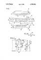
- FIG. 1is a perspective view of a first embodiment a multiple pin connector assembly having a filtering interface incorporating a filter for electromagnetic interference;
- FIG. 1ais a side elevational view of a leadless capacitor used with the filtering interface.
- FIG. 2is an enlarged, fragmentary, top plan view of the filtering interface of FIG. 1.
- the first embodiment of the electrical connector assembly of the present inventionis broadly denoted by the numeral 10 and includes a filtering interface or interface member 12 between a pair of electrical connector members 14 and 16 of generally conventional construction.
- the purpose of filtering interface 12is to filter electromagnetic signal frequencies to ground through capacitors carried by the interface member 12 in a manner hereinafter described.
- Connector members 14 and 16can be any type of connector. They serve as the connection between the filtering interface and the outside world. The construction of each connector is not important to the teachings of the present invention only inasmuch as it either:
- the connector pinswill make electrical contact with plating in each hole of the filtering interface, by either a press fit or solder connection in the hole of the filtering interface.
- Filtering interface 12is comprised of a body 26 of electrically non-conducting material.
- the bodycan be of any shape but, for purposes of illustration, it is rectangular and has four flat, outer faces, including a pair of opposed end faces 28, only one of which is shown in FIG. 1, and a pair of side faces 30 (FIG. 2).
- Filtering interface 12has a plurality of holes 32 extending therethrough between end faces 28. These holes are located in the same arrangement as pins 20 of connectors members 14 and 16 so that the holes receive pins 20 as connector members 14 and 16 are moved into operative positions continguous to respective end faces 28. When the connector members 14 and 16 are in their operative positions adjacent to filtering interface 12, the three components are interconnected by screws 25 passing through holes 24 of members 14 and 16 and holes 33 in filtering interface 12. In lieu of using screws, the frictional engagement between pins 20 and interface member 12 when the pins are in holes 32 may be enough to releasably couple connectors 14 and 16 to filtering interface 12.
- One end face 28 of filtering interface 12has a plurality of generally parallel grooves 36, there being a groove 36 for each hole 32, respectively.
- the grooves 36extend from the respective hole 32 to the adjacent side face 30 as shown in FIG. 2.
- the depth of each grooveis sufficient so that the groove can receive a leadless capacitor 38 (FIG. 1a) which is to be press fitted into the groove.
- Leadless capacitorsare well known and are commercially available.
- Such a capacitorincludes a capacitor body 40 having a pair of end terminals 42 and 44 of electrically conductive material. Leadless capacitors can be extremely small in size such as 1/4 inch in length and about 0.050 inch in diameter.
- a number of surfaces of filtering interface 12are plated with a metallic material which has good electrical conductivity, such as copper or the like.
- Each of the side faces 30is plated to provide layer 46 (FIG. 2).
- each groove 36is plated to present layers 48 and layers 50 which are separated from each other. When a leadless capacitor 38 is placed in a groove 36, it will bridge the gap between layers 48 and 50 so as to provide a current flow path therebetween.
- each hole 32is provided with a plating 52 which extends from one face 28 to the opposite end face 28.
- each layer 52is integral with the adjacent layer 48, and each layer 46 is integral with adjacent layers 50.
- leadless capacitors 38are placed in grooves 36 in the manner shown in the upper right-hand portion of FIG. 2. Then, connector members 14 and 16 are coupled to filtering interface 12 by forcing pins 20 into respective holes 32 or by soldering. When this occurs, the pins make electrical contact with adjacent layers 52 which, through layers 50 and 48, make electrical contact with layers 46.
- Layer 46shown in FIG. 2, is in electrical contact with a layer 54 on each end portion 56 of filtering interface 12.
- Each layer 54makes electrical contact through a screw (not shown) to a grounded chassis or other element in some suitable fashion.
- each pin 20will be filtered by way of a respective leadless capacitor 38 in a corresponding groove 36. All capacitors have a common ground connection; however, the pins 20, when they are in respective holes 32 of filtering interface 12, will be electrically isolated from each other.
- the purpose and use of the present inventionis to filter electromagnetic signal frequencies to ground through capacitors 38.
- the unique feature of the present inventionis the simple and rugged interconnection achieved between individual pins and ground.
- the filteringis achieved through the use of filtering interface 12 which assures that each pin 20 is filtered while the pins are electrically insulated from each other.
- the electrically non-conducting material forming body 26 of filtering interface 12is a platable plastic material.
- a suitable material for this purposeis one identified as Ultem and made by General Electric Company.
- Another suitable materialis one taken from the 1700, 1800 or 8000 series materials of Union Carbide Corporation.
- Other platable plasticscould be used, if desired.
- the filtering capacitors 38can be quickly and easily assembled into grooves 36 and held in place by a press fit, by an adhesive or solder paste, by heat staking or by any other suitable technique to provide a fixed mechanical attachment during or after plating. An electrical connection is obtained between the plated groove and the capacitors either by plating by soldering.
- filtering interface 12When the filter capacitors are press-fitted in place, filtering interface 12 provides a dual function. It provides an insulated, conductive path from each pin 20 through a respective capacitor to ground. It also provides a firm mechanical attachment for the capacitor by interference fit before, during and after plating.
- Assembly of the capacitorscan be achieved before plating. In such as a case, the capacitors are plated in place. If the capacitors are assembled after plating, then either the press fit or a subsequent soldering operation will provide the electrical connection.
- the capacitorswill vary in capacitance depending upon the application to provide the filtering effect.
- leadless capacitors and the filtering interface methodconsiderable space saving is achieved as opposed to conventional filter methods.
- the filter interface member 12can be adapted to existing equipment applications where space is at a premium or where standard connector devices need to be interchangeable with existing equipment.
Landscapes
- Details Of Connecting Devices For Male And Female Coupling (AREA)
Abstract
Description
Claims (16)
Priority Applications (1)
| Application Number | Priority Date | Filing Date | Title |
|---|---|---|---|
| US06/488,958US4580866A (en) | 1983-04-27 | 1983-04-27 | Electrical connector assembly having electromagnetic interference filter |
Applications Claiming Priority (1)
| Application Number | Priority Date | Filing Date | Title |
|---|---|---|---|
| US06/488,958US4580866A (en) | 1983-04-27 | 1983-04-27 | Electrical connector assembly having electromagnetic interference filter |
Publications (1)
| Publication Number | Publication Date |
|---|---|
| US4580866Atrue US4580866A (en) | 1986-04-08 |
Family
ID=23941820
Family Applications (1)
| Application Number | Title | Priority Date | Filing Date |
|---|---|---|---|
| US06/488,958Expired - LifetimeUS4580866A (en) | 1983-04-27 | 1983-04-27 | Electrical connector assembly having electromagnetic interference filter |
Country Status (1)
| Country | Link |
|---|---|
| US (1) | US4580866A (en) |
Cited By (28)
| Publication number | Priority date | Publication date | Assignee | Title |
|---|---|---|---|---|
| US4695115A (en)* | 1986-08-29 | 1987-09-22 | Corcom, Inc. | Telephone connector with bypass capacitor |
| US4726638A (en)* | 1985-07-26 | 1988-02-23 | Amp Incorporated | Transient suppression assembly |
| US4729752A (en)* | 1985-07-26 | 1988-03-08 | Amp Incorporated | Transient suppression device |
| US4729743A (en)* | 1985-07-26 | 1988-03-08 | Amp Incorporated | Filtered electrical connector |
| WO1988005218A1 (en)* | 1986-12-24 | 1988-07-14 | Amp Incorporated | Filtered electrical device and method for making same |
| US4804332A (en)* | 1986-12-24 | 1989-02-14 | Amp Incorporated | Filtered electrical device and method for making same |
| US4806124A (en)* | 1987-05-01 | 1989-02-21 | Labinal Components And Systems, Inc. | Electrical connections |
| EP0317116A1 (en)* | 1987-11-19 | 1989-05-24 | The Whitaker Corporation | Electrical connector and terminal for serially mounting electrical circuit components |
| US4858313A (en)* | 1987-05-01 | 1989-08-22 | Labinal Components And Systems, Inc. | Method of forming a connector |
| US4916576A (en)* | 1989-02-27 | 1990-04-10 | Fmtt, Inc. | Matrix capacitor |
| US4930200A (en)* | 1989-07-28 | 1990-06-05 | Thomas & Betts Corporation | Method of making an electrical filter connector |
| US4992061A (en)* | 1989-07-28 | 1991-02-12 | Thomas & Betts Corporation | Electrical filter connector |
| US5224878A (en)* | 1992-03-31 | 1993-07-06 | Amp Incorporated | Connector filter with integral surge protection |
| US5236376A (en)* | 1991-03-04 | 1993-08-17 | Amir Cohen | Connector |
| US5331505A (en)* | 1993-01-08 | 1994-07-19 | Honeywell Inc. | Multi-coplanar capacitor for electrical connector |
| US5340334A (en)* | 1993-07-19 | 1994-08-23 | The Whitaker Corporation | Filtered electrical connector |
| US5399099A (en)* | 1993-08-12 | 1995-03-21 | The Whitaker Corporation | EMI protected tap connector |
| US5414587A (en)* | 1991-04-29 | 1995-05-09 | Trw Inc. | Surge suppression device |
| US5428288A (en)* | 1991-04-29 | 1995-06-27 | Trw Inc. | Microelectric monitoring device |
| US5455734A (en)* | 1991-04-29 | 1995-10-03 | Trw Inc. | Insert device for electrical relays, solenoids, motors, controllers, and the like |
| WO1996013883A1 (en)* | 1994-10-31 | 1996-05-09 | Berg Technology Inc. | Low cost filtered shielded electronic connector and method of use |
| US5590058A (en)* | 1991-04-29 | 1996-12-31 | Trw Inc. | Battery monitor for unobstrusive installation with a battery connector |
| US5692917A (en)* | 1991-04-29 | 1997-12-02 | Trw Inc. | Computer hardware insert device for software authorization |
| US5823827A (en)* | 1996-02-29 | 1998-10-20 | Berg Technology, Inc. | Low cost filtered and shielded electronic connector |
| US20080127490A1 (en)* | 2006-12-01 | 2008-06-05 | Lotes Co., Ltd. | Manufacture process of connector |
| US20110003510A1 (en)* | 2008-03-12 | 2011-01-06 | D Amico Sebastiano | Power supply connector |
| US20140057494A1 (en)* | 2012-08-22 | 2014-02-27 | Amphenol Corporation | High-frequency electrical connector |
| US20140147192A1 (en)* | 2012-04-26 | 2014-05-29 | California Institute Of Technology | Silicon alignment pins: an easy way to realize a wafer-to-wafer alignment |
Citations (3)
| Publication number | Priority date | Publication date | Assignee | Title |
|---|---|---|---|---|
| US4126840A (en)* | 1977-03-14 | 1978-11-21 | International Telephone And Telegraph Corporation | Filter connector |
| US4144509A (en)* | 1977-01-12 | 1979-03-13 | Bunker Ramo Corporation | Filter connector |
| US4371226A (en)* | 1980-10-20 | 1983-02-01 | International Telephone And Telegraph Corporation | Filter connector and method of assembly thereof |
- 1983
- 1983-04-27USUS06/488,958patent/US4580866A/ennot_activeExpired - Lifetime
Patent Citations (3)
| Publication number | Priority date | Publication date | Assignee | Title |
|---|---|---|---|---|
| US4144509A (en)* | 1977-01-12 | 1979-03-13 | Bunker Ramo Corporation | Filter connector |
| US4126840A (en)* | 1977-03-14 | 1978-11-21 | International Telephone And Telegraph Corporation | Filter connector |
| US4371226A (en)* | 1980-10-20 | 1983-02-01 | International Telephone And Telegraph Corporation | Filter connector and method of assembly thereof |
Cited By (39)
| Publication number | Priority date | Publication date | Assignee | Title |
|---|---|---|---|---|
| US4726638A (en)* | 1985-07-26 | 1988-02-23 | Amp Incorporated | Transient suppression assembly |
| US4729752A (en)* | 1985-07-26 | 1988-03-08 | Amp Incorporated | Transient suppression device |
| US4729743A (en)* | 1985-07-26 | 1988-03-08 | Amp Incorporated | Filtered electrical connector |
| US4695115A (en)* | 1986-08-29 | 1987-09-22 | Corcom, Inc. | Telephone connector with bypass capacitor |
| WO1988005218A1 (en)* | 1986-12-24 | 1988-07-14 | Amp Incorporated | Filtered electrical device and method for making same |
| US4804332A (en)* | 1986-12-24 | 1989-02-14 | Amp Incorporated | Filtered electrical device and method for making same |
| US4806124A (en)* | 1987-05-01 | 1989-02-21 | Labinal Components And Systems, Inc. | Electrical connections |
| US4858313A (en)* | 1987-05-01 | 1989-08-22 | Labinal Components And Systems, Inc. | Method of forming a connector |
| EP0317116A1 (en)* | 1987-11-19 | 1989-05-24 | The Whitaker Corporation | Electrical connector and terminal for serially mounting electrical circuit components |
| US4916576A (en)* | 1989-02-27 | 1990-04-10 | Fmtt, Inc. | Matrix capacitor |
| US4930200A (en)* | 1989-07-28 | 1990-06-05 | Thomas & Betts Corporation | Method of making an electrical filter connector |
| US4992061A (en)* | 1989-07-28 | 1991-02-12 | Thomas & Betts Corporation | Electrical filter connector |
| US5236376A (en)* | 1991-03-04 | 1993-08-17 | Amir Cohen | Connector |
| US5428288A (en)* | 1991-04-29 | 1995-06-27 | Trw Inc. | Microelectric monitoring device |
| US5590058A (en)* | 1991-04-29 | 1996-12-31 | Trw Inc. | Battery monitor for unobstrusive installation with a battery connector |
| US5414587A (en)* | 1991-04-29 | 1995-05-09 | Trw Inc. | Surge suppression device |
| US5455734A (en)* | 1991-04-29 | 1995-10-03 | Trw Inc. | Insert device for electrical relays, solenoids, motors, controllers, and the like |
| US5568348A (en)* | 1991-04-29 | 1996-10-22 | Trw Inc. | Insert device for electrical relays, solenoids, motors, controllers, and the like |
| US5692917A (en)* | 1991-04-29 | 1997-12-02 | Trw Inc. | Computer hardware insert device for software authorization |
| US5224878A (en)* | 1992-03-31 | 1993-07-06 | Amp Incorporated | Connector filter with integral surge protection |
| US5331505A (en)* | 1993-01-08 | 1994-07-19 | Honeywell Inc. | Multi-coplanar capacitor for electrical connector |
| US5340334A (en)* | 1993-07-19 | 1994-08-23 | The Whitaker Corporation | Filtered electrical connector |
| US5399099A (en)* | 1993-08-12 | 1995-03-21 | The Whitaker Corporation | EMI protected tap connector |
| WO1996013883A1 (en)* | 1994-10-31 | 1996-05-09 | Berg Technology Inc. | Low cost filtered shielded electronic connector and method of use |
| US5842888A (en)* | 1994-10-31 | 1998-12-01 | Berg Technology, Inc. | Low cost filtered and shielded electronic connector |
| US5639264A (en)* | 1994-10-31 | 1997-06-17 | Berg Technology, Inc. | Low cost filtered and shielded electronic connector and method of use |
| US5580279A (en)* | 1994-10-31 | 1996-12-03 | Berg Technology, Inc. | Low cost filtered and shielded electronic connector and method of use |
| US5769667A (en)* | 1994-10-31 | 1998-06-23 | Berg Technology, Inc. | Low cost filtered and shielded electronic connector |
| US5803769A (en)* | 1994-10-31 | 1998-09-08 | Berg Technology, Inc. | Low cost filtered and shielded electronic connector and method of use |
| US5816857A (en)* | 1994-10-31 | 1998-10-06 | Berg Technology, Inc. | Low cost filtered and shielded electronic connector |
| US5626494A (en)* | 1994-10-31 | 1997-05-06 | Berg Technology, Inc. | Low cost filtered and shielded electronic connector and method of use |
| US5823827A (en)* | 1996-02-29 | 1998-10-20 | Berg Technology, Inc. | Low cost filtered and shielded electronic connector |
| US20080127490A1 (en)* | 2006-12-01 | 2008-06-05 | Lotes Co., Ltd. | Manufacture process of connector |
| US20110003510A1 (en)* | 2008-03-12 | 2011-01-06 | D Amico Sebastiano | Power supply connector |
| US8292665B2 (en)* | 2008-03-12 | 2012-10-23 | Sumuto S.R.L. | Power supply connector |
| US20140147192A1 (en)* | 2012-04-26 | 2014-05-29 | California Institute Of Technology | Silicon alignment pins: an easy way to realize a wafer-to-wafer alignment |
| US9512863B2 (en)* | 2012-04-26 | 2016-12-06 | California Institute Of Technology | Silicon alignment pins: an easy way to realize a wafer-to-wafer alignment |
| US20140057494A1 (en)* | 2012-08-22 | 2014-02-27 | Amphenol Corporation | High-frequency electrical connector |
| US9240644B2 (en)* | 2012-08-22 | 2016-01-19 | Amphenol Corporation | High-frequency electrical connector |
Similar Documents
| Publication | Publication Date | Title |
|---|---|---|
| US4580866A (en) | Electrical connector assembly having electromagnetic interference filter | |
| CA1236187A (en) | Backplane-daughter board connector | |
| US5236376A (en) | Connector | |
| US3790858A (en) | Electrical connector with component grounding plate | |
| US4144509A (en) | Filter connector | |
| US4116516A (en) | Multiple layered connector | |
| US4418972A (en) | Electrical connector for printed wiring board | |
| US4838800A (en) | High density interconnect system | |
| US6364713B1 (en) | Electrical connector adapter assembly | |
| US3587028A (en) | Coaxial connector guide and grounding structure | |
| US4673902A (en) | Dielectric material coaxial resonator filter directly mountable on a circuit board | |
| JP2801915B2 (en) | Filter unit for connector | |
| US4710133A (en) | Electrical connectors | |
| EP0752739A1 (en) | Connector, preferably a right angle connector, with integrated pcb assembly | |
| US5211567A (en) | Metallized connector block | |
| EP0305186A3 (en) | Screened electrical connectors | |
| WO2002058191A3 (en) | Shielded electrical connector | |
| US4755145A (en) | Electrically connecting circuit board system | |
| CN101529650A (en) | Impedance matched circuit board | |
| WO2002101883B1 (en) | High-density, impedance tuned connector | |
| US4606598A (en) | Grounding plate connector | |
| GB2184882A (en) | High capacitance bus bar including multilayer ceramic capacitors | |
| US3702422A (en) | Filters for interconnection systems | |
| US3746932A (en) | Panel board systems and components therefor | |
| US4589720A (en) | Planar electronic filter element and a connector embodying such a filter |
Legal Events
| Date | Code | Title | Description |
|---|---|---|---|
| AS | Assignment | Owner name:TOPOCON, INC.; 500 ENDLICH DR., SANTA CRUZ, CA. 95 Free format text:ASSIGNMENT OF ASSIGNORS INTEREST.;ASSIGNOR:HAGNER, GEORGE;REEL/FRAME:004123/0286 Effective date:19830426 | |
| STCF | Information on status: patent grant | Free format text:PATENTED CASE | |
| AS | Assignment | Owner name:TRW INC., ONE SPACE PARK, REDONDO BEACH, CA A CORP Free format text:ASSIGNMENT OF ASSIGNORS INTEREST.;ASSIGNOR:HANSET, RICHARD;REEL/FRAME:004647/0812 Effective date:19860818 | |
| AS | Assignment | Owner name:LABINAL COMPONENTS AND SYSTEMS, INC., A DE CORP. Free format text:ASSIGNMENT OF ASSIGNORS INTEREST.;ASSIGNOR:TRW INC., A CORP. OF OH;REEL/FRAME:004853/0501 Effective date:19871224 | |
| FEPP | Fee payment procedure | Free format text:PAYOR NUMBER ASSIGNED (ORIGINAL EVENT CODE: ASPN); ENTITY STATUS OF PATENT OWNER: LARGE ENTITY | |
| FEPP | Fee payment procedure | Free format text:MAINTENANCE FEE HAS ALREADY BEEN PAID. REFUND IS SCHEDULED (ORIGINAL EVENT CODE: F160); ENTITY STATUS OF PATENT OWNER: LARGE ENTITY | |
| FPAY | Fee payment | Year of fee payment:4 | |
| FEPP | Fee payment procedure | Free format text:PAT HLDR NO LONGER CLAIMS SMALL ENT STAT AS SMALL BUSINESS (ORIGINAL EVENT CODE: LSM2); ENTITY STATUS OF PATENT OWNER: LARGE ENTITY | |
| FEPP | Fee payment procedure | Free format text:PAYER NUMBER DE-ASSIGNED (ORIGINAL EVENT CODE: RMPN); ENTITY STATUS OF PATENT OWNER: LARGE ENTITY Free format text:PAYOR NUMBER ASSIGNED (ORIGINAL EVENT CODE: ASPN); ENTITY STATUS OF PATENT OWNER: LARGE ENTITY | |
| FPAY | Fee payment | Year of fee payment:8 | |
| FPAY | Fee payment | Year of fee payment:12 | |
| AS | Assignment | Owner name:CINCH CONNECTORS, INC., ILLINOIS Free format text:ASSIGNMENT OF ASSIGNORS INTEREST;ASSIGNOR:LABINAL COMPONENTS AND SYSTEMS, INC.;REEL/FRAME:011511/0595 Effective date:20001212 |