US4580331A - PNP-type lateral transistor with minimal substrate operation interference and method for producing same - Google Patents
PNP-type lateral transistor with minimal substrate operation interference and method for producing sameDownload PDFInfo
- Publication number
- US4580331A US4580331AUS06/558,072US55807283AUS4580331AUS 4580331 AUS4580331 AUS 4580331AUS 55807283 AUS55807283 AUS 55807283AUS 4580331 AUS4580331 AUS 4580331A
- Authority
- US
- United States
- Prior art keywords
- substrate
- slots
- regions
- active regions
- doping
- Prior art date
- Legal status (The legal status is an assumption and is not a legal conclusion. Google has not performed a legal analysis and makes no representation as to the accuracy of the status listed.)
- Expired - Fee Related
Links
- 239000000758substrateSubstances0.000titleclaimsabstractdescription50
- 238000004519manufacturing processMethods0.000titleabstractdescription3
- 238000005530etchingMethods0.000claimsabstractdescription6
- 238000001704evaporationMethods0.000claimsabstractdescription5
- 238000000034methodMethods0.000claimsdescription14
- 238000003491arrayMethods0.000claimsdescription3
- 230000001590oxidative effectEffects0.000claims4
- 230000000873masking effectEffects0.000claims2
- 230000001419dependent effectEffects0.000claims1
- 238000000992sputter etchingMethods0.000claims1
- 229910052698phosphorusInorganic materials0.000abstractdescription9
- 230000003647oxidationEffects0.000abstractdescription7
- 238000007254oxidation reactionMethods0.000abstractdescription7
- 238000002955isolationMethods0.000abstractdescription5
- 230000008020evaporationEffects0.000abstractdescription4
- 230000000694effectsEffects0.000abstractdescription3
- 230000003071parasitic effectEffects0.000abstractdescription3
- 238000007796conventional methodMethods0.000abstractdescription2
- XUIMIQQOPSSXEZ-UHFFFAOYSA-NSiliconChemical compound[Si]XUIMIQQOPSSXEZ-UHFFFAOYSA-N0.000description8
- 229910052710siliconInorganic materials0.000description8
- 239000010703siliconSubstances0.000description8
- 239000010410layerSubstances0.000description7
- 229920002120photoresistant polymerPolymers0.000description6
- ZOXJGFHDIHLPTG-UHFFFAOYSA-NBoronChemical compound[B]ZOXJGFHDIHLPTG-UHFFFAOYSA-N0.000description5
- VYPSYNLAJGMNEJ-UHFFFAOYSA-NSilicium dioxideChemical compoundO=[Si]=OVYPSYNLAJGMNEJ-UHFFFAOYSA-N0.000description5
- 229910052796boronInorganic materials0.000description5
- 239000007943implantSubstances0.000description3
- 229910052814silicon oxideInorganic materials0.000description3
- BHEPBYXIRTUNPN-UHFFFAOYSA-Nhydridophosphorus(.) (triplet)Chemical compound[PH]BHEPBYXIRTUNPN-UHFFFAOYSA-N0.000description2
- 150000002500ionsChemical class0.000description2
- 238000001465metallisationMethods0.000description2
- OAICVXFJPJFONN-UHFFFAOYSA-NPhosphorusChemical compound[P]OAICVXFJPJFONN-UHFFFAOYSA-N0.000description1
- 238000001015X-ray lithographyMethods0.000description1
- 229910052785arsenicInorganic materials0.000description1
- RQNWIZPPADIBDY-UHFFFAOYSA-Narsenic atomChemical compound[As]RQNWIZPPADIBDY-UHFFFAOYSA-N0.000description1
- 229910052681coesiteInorganic materials0.000description1
- 229910052906cristobaliteInorganic materials0.000description1
- 238000000609electron-beam lithographyMethods0.000description1
- 238000012986modificationMethods0.000description1
- 230000004048modificationEffects0.000description1
- 238000000059patterningMethods0.000description1
- -1phosphorous ionChemical class0.000description1
- 239000011574phosphorusSubstances0.000description1
- 230000001681protective effectEffects0.000description1
- 239000011241protective layerSubstances0.000description1
- 230000005855radiationEffects0.000description1
- 238000009877renderingMethods0.000description1
- 239000000377silicon dioxideSubstances0.000description1
- 239000002210silicon-based materialSubstances0.000description1
- 229910052682stishoviteInorganic materials0.000description1
- 229910052905tridymiteInorganic materials0.000description1
Images


Classifications
- H—ELECTRICITY
- H10—SEMICONDUCTOR DEVICES; ELECTRIC SOLID-STATE DEVICES NOT OTHERWISE PROVIDED FOR
- H10D—INORGANIC ELECTRIC SEMICONDUCTOR DEVICES
- H10D10/00—Bipolar junction transistors [BJT]
- H10D10/311—Thin-film BJTs
- H—ELECTRICITY
- H01—ELECTRIC ELEMENTS
- H01L—SEMICONDUCTOR DEVICES NOT COVERED BY CLASS H10
- H01L21/00—Processes or apparatus adapted for the manufacture or treatment of semiconductor or solid state devices or of parts thereof
- H01L21/02—Manufacture or treatment of semiconductor devices or of parts thereof
- H01L21/04—Manufacture or treatment of semiconductor devices or of parts thereof the devices having potential barriers, e.g. a PN junction, depletion layer or carrier concentration layer
- H01L21/18—Manufacture or treatment of semiconductor devices or of parts thereof the devices having potential barriers, e.g. a PN junction, depletion layer or carrier concentration layer the devices having semiconductor bodies comprising elements of Group IV of the Periodic Table or AIIIBV compounds with or without impurities, e.g. doping materials
- H01L21/26—Bombardment with radiation
- H01L21/263—Bombardment with radiation with high-energy radiation
- H01L21/265—Bombardment with radiation with high-energy radiation producing ion implantation
- H—ELECTRICITY
- H01—ELECTRIC ELEMENTS
- H01L—SEMICONDUCTOR DEVICES NOT COVERED BY CLASS H10
- H01L21/00—Processes or apparatus adapted for the manufacture or treatment of semiconductor or solid state devices or of parts thereof
- H01L21/70—Manufacture or treatment of devices consisting of a plurality of solid state components formed in or on a common substrate or of parts thereof; Manufacture of integrated circuit devices or of parts thereof
- H01L21/71—Manufacture of specific parts of devices defined in group H01L21/70
- H01L21/76—Making of isolation regions between components
- H01L21/762—Dielectric regions, e.g. EPIC dielectric isolation, LOCOS; Trench refilling techniques, SOI technology, use of channel stoppers
- H01L21/76224—Dielectric regions, e.g. EPIC dielectric isolation, LOCOS; Trench refilling techniques, SOI technology, use of channel stoppers using trench refilling with dielectric materials
- H01L21/76237—Dielectric regions, e.g. EPIC dielectric isolation, LOCOS; Trench refilling techniques, SOI technology, use of channel stoppers using trench refilling with dielectric materials introducing impurities in trench side or bottom walls, e.g. for forming channel stoppers or alter isolation behavior
- H—ELECTRICITY
- H10—SEMICONDUCTOR DEVICES; ELECTRIC SOLID-STATE DEVICES NOT OTHERWISE PROVIDED FOR
- H10D—INORGANIC ELECTRIC SEMICONDUCTOR DEVICES
- H10D84/00—Integrated devices formed in or on semiconductor substrates that comprise only semiconducting layers, e.g. on Si wafers or on GaAs-on-Si wafers
- H10D84/01—Manufacture or treatment
- H10D84/0112—Integrating together multiple components covered by H10D8/00, H10D10/00 or H10D18/00, e.g. integrating multiple BJTs
- H—ELECTRICITY
- H10—SEMICONDUCTOR DEVICES; ELECTRIC SOLID-STATE DEVICES NOT OTHERWISE PROVIDED FOR
- H10D—INORGANIC ELECTRIC SEMICONDUCTOR DEVICES
- H10D84/00—Integrated devices formed in or on semiconductor substrates that comprise only semiconducting layers, e.g. on Si wafers or on GaAs-on-Si wafers
- H10D84/01—Manufacture or treatment
- H10D84/02—Manufacture or treatment characterised by using material-based technologies
- H10D84/03—Manufacture or treatment characterised by using material-based technologies using Group IV technology, e.g. silicon technology or silicon-carbide [SiC] technology
- H10D84/038—Manufacture or treatment characterised by using material-based technologies using Group IV technology, e.g. silicon technology or silicon-carbide [SiC] technology using silicon technology, e.g. SiGe
- H—ELECTRICITY
- H10—SEMICONDUCTOR DEVICES; ELECTRIC SOLID-STATE DEVICES NOT OTHERWISE PROVIDED FOR
- H10D—INORGANIC ELECTRIC SEMICONDUCTOR DEVICES
- H10D86/00—Integrated devices formed in or on insulating or conducting substrates, e.g. formed in silicon-on-insulator [SOI] substrates or on stainless steel or glass substrates
- H10D86/201—Integrated devices formed in or on insulating or conducting substrates, e.g. formed in silicon-on-insulator [SOI] substrates or on stainless steel or glass substrates the substrates comprising an insulating layer on a semiconductor body, e.g. SOI
Definitions
- This inventionis a novel structure and method for forming a VLSI PNP type lateral dielectrically isolated transistor utilizing VLSI chip processing steps to fabricate hundreds of such devices simultaneously.
- the inventionis a novel lateral PNP type transistor formed on a substrate by orthogonal slots which define each active region and permit doping of the active regions via opposed slots while supported by oxidation achieved through underlying etching of each active region in a semi-array of regions supported at spaced apart positions and totally isolated from the substrate by substrate oxidation. Electrical connections are conventionally made to the P emitter, N+N base and P collector.
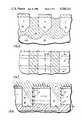
- FIG. 1is a view in section through an N type substrate with photoresist applied through a slotted mask
- FIG. 2shows the structure of FIG. 1 with slots formed in the substrate where not protected by the resist
- FIG. 3is a perspective view of the substrate showing the first set of longitudinal slots
- FIG. 4is a view in section showing the application of an angle evaporation etch resist layer partially protecting the edges of the slots;
- FIG. 5is a view in section with the etch resist layer in place and showing the effects of the etch having been applied via the slots to undercut the longitudinal regions which will become active regions of the transistors being formed;
- FIG. 6shows the structure of FIG. 5 after the etch resist has been removed and following oxidation of the substrate to fill in the voids created by the etch;
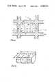
- FIG. 7is a view in plan of the structure of FIG. 6 showing the orthogonal set of slots relative to the original set of slots;
- FIG. 8is a view in section taken across the orthogonal set of slots showing the phosphorous ion implant step to produce the N+doping shown;
- FIG. 9shows the structure of FIG. 8 taken after phosphorous drive-in and the application of boron deposit or implant
- FIG. 10shows the structure of FIG. 9 following boron drive-in from both sides to produce the P regions and following oxidation of the substrate to fill the slots and protect the top;
- FIG. 11is a top plan view of the completed structure showing in dashed outline the electrode connections for the emitter, base and collector for a single active region of a single transistor;
- FIG. 12is a view in perspective of the transistor active region, per se.
- FIG. 13shows an alternate embodiment using substrate doping change in lieu of oxide for device isolation
- FIG. 14shows you the steps of the process of FIG. 13.
- the effects of the substrateare minimized relative to the operation of the device.
- the active regionmay be completely contained with the surface of area of 3d ⁇ 5d or 15d 2 wherein d is only a few micrometers or less.
- the isolated regionis completely separated from the substrate by oxidation and the parasitic capacitances and resistances are almost completely reduced to a minimum value attainable because the transistor is reduced essentially to just its electronically active region whereas in the conventional (vertical) transistor, the electrically active region is only a very small fraction of the total transistor area.
- the dielectric isolation between transistors offered by the same substrate oxidationhas advantages with respect to high frequency performance, high voltage integrated circuits, radiation resistance, circuit flexibility, i.e., the process can provide NPN, PNP, JFET, MOSFET's etc. on the same integrated circuit chip.
- FIG. 1there is shown a silicon substrate of the N type, having patterned photoresist applied to an upper surface thereof.
- the patternmay simply comprise longitudinal slots for rendering the photoresist 23 alternately soluble and it may be seen that the soluble photoresist has been removed to provide exposure of the substrate 21 so that the slots 25 and 27 may be milled therein or formed by O.D.E. etching process. These slots 25 and 27 penetrate the upper surface of the silicon substrate 21 sufficiently deeply that they extend beneath the depth of the region which will ultimately become the active regions for the various transistors.
- FIG. 3the photoresist layer 23 has been removed and the structure is shown in perspective thereby showing the slots 25 and 27 extending inwardly of the upper surface of silicon substrate 21.
- the slots 25 and 27are necessary. They permit angle evaporation of etch-resist 31 to the edges of the slots 25 and 27. The result provides a protective covering over the tops of the active regions being formed. Also, it should be noted that due to the angle of evaporation of the etch resist 31, this protective layer only extends to a certain depth within slots 25 and 27, but this depth must be adequate to protect the active regions being formed. Thus, in FIG. 5, it may be seen that the active regions are generally shown at 35, 37 and 39 above the silicon substrate etch level 41 and also above the etch levels 35', 37' and 39' where the etch introduced through the slots 25 and 27 removed the substrate from beneath the active regions 35, 37 and 39.
- FIG. 6it may be seen that the etch resist 31 has been removed and the silicon has been oxidized to SiO 2 shown at 41 as filling or partly filling the voids between regions 35, 37 and 39 and the silicon substrate 21.
- the orthogonally related sets of slots 45 and 47may be formed as illustrated in the top plan view of FIG. 7.
- the procedure for forming these slotsis the same as before, requiring a photoresist layer patterned in the form of spaced apart slots and the silicon material either ion milled away or etched using O.D.E. techniques, as best shown in FIG. 8.
- FIG. 8the application of N+ doping is achieved by phosphorous implant shown by the arrows 49 to produce the N+ region 51. It should be noted that this implanting is done only into the corresponding right hand edges of slots 45 and 47 to provide the N+layers 51 and 53.
- N+ regionshave been driven in, such as by using high heat so that they are expanded as shown by 51' and 53'. Also, a further N+ region is visible to the left at 55', having been produced by a slot to the left of the margin of the page.
- the boron P or P+ regions 62 and 63have now been driven in to comprise the expanded regions 62' and 63'. Accordingly the N+ region has been changed in size and is now designated 51" as is also true of the remaining N region now identified as 21"".
- the region 62'will comprise the emitter with the regions 51" and 21"" comprising a graded base region and finally region 63' being the collector region.
- the substratehas again been oxidized to fill in the slots 45 and 47 and provide a covering over the active region of the electrodes generally shown at 75.
- the doping gradient in the base regionis similar to convention double diffused transistors.
- FIG. 11A finished transistor is shown in FIG. 11 wherein the contacts 101, 102 and 103 are provided from a metallization layer for the emitter 111, base 112 and collector 113, respectively. These contacts are fabricated simply by conventional techniques for patterning or metallization.
- the transistor comprising these three electrodesis surrounded by moats of silicon oxide formed in the slots 25, 27 and 45 47. Thus, the transistor is isolated from its substrate, adjacent transistors or other elements.
- the active region of the transistoris visible in FIG. 12 in the perspective view showing the emitter 111 base 112 and collector 113.
- a P substratecan be doped N in the active regions and the use of O.D.E. avoided by skipping from FIG. 3 to FIG. 8.
- the active regionsare doped N (see FIG. 13) via the slots 45 and 47; and next, phosphorus or arsenic is ion angle implanted so only regions 51', 53' become N+ doped.
- boronis implanted from all edges of slots 45' and 47' (FIG. 14) to form P+ regions 61', 62', 63' and 64'. Thereafter, the slots 45' and 47' are deepened original P substrate and filled with oxide.
- each active regionis P+N+N and P+doped in an N doped region but is underlaid by P doped substrate for total isolation without using etching techniques.
- the principles of the present inventionare compatible with use of the Perkin Elmer Projection Printer equipment for 2 micron dimensions, the 10:1 stepper for 1 micron rated dimensions, and electron beam or X-ray lithography for under 1 micron dimensions, even utilizing a portion of a line as a contact, all utilizing accepted existing registration and alignment techniques.
Landscapes
- Physics & Mathematics (AREA)
- Engineering & Computer Science (AREA)
- Condensed Matter Physics & Semiconductors (AREA)
- General Physics & Mathematics (AREA)
- Manufacturing & Machinery (AREA)
- Computer Hardware Design (AREA)
- Microelectronics & Electronic Packaging (AREA)
- Power Engineering (AREA)
- High Energy & Nuclear Physics (AREA)
- Health & Medical Sciences (AREA)
- Toxicology (AREA)
- Element Separation (AREA)
- Bipolar Transistors (AREA)
Abstract
Description
Claims (3)
Priority Applications (1)
| Application Number | Priority Date | Filing Date | Title |
|---|---|---|---|
| US06/558,072US4580331A (en) | 1981-07-01 | 1983-12-05 | PNP-type lateral transistor with minimal substrate operation interference and method for producing same |
Applications Claiming Priority (2)
| Application Number | Priority Date | Filing Date | Title |
|---|---|---|---|
| US27948281A | 1981-07-01 | 1981-07-01 | |
| US06/558,072US4580331A (en) | 1981-07-01 | 1983-12-05 | PNP-type lateral transistor with minimal substrate operation interference and method for producing same |
Related Parent Applications (1)
| Application Number | Title | Priority Date | Filing Date |
|---|---|---|---|
| US27948281AContinuation-In-Part | 1981-07-01 | 1981-07-01 |
Related Child Applications (1)
| Application Number | Title | Priority Date | Filing Date |
|---|---|---|---|
| US69821785ADivision | 1981-07-01 | 1985-01-31 |
Publications (1)
| Publication Number | Publication Date |
|---|---|
| US4580331Atrue US4580331A (en) | 1986-04-08 |
Family
ID=26959691
Family Applications (1)
| Application Number | Title | Priority Date | Filing Date |
|---|---|---|---|
| US06/558,072Expired - Fee RelatedUS4580331A (en) | 1981-07-01 | 1983-12-05 | PNP-type lateral transistor with minimal substrate operation interference and method for producing same |
Country Status (1)
| Country | Link |
|---|---|
| US (1) | US4580331A (en) |
Cited By (28)
| Publication number | Priority date | Publication date | Assignee | Title |
|---|---|---|---|---|
| US4604162A (en)* | 1983-06-13 | 1986-08-05 | Ncr Corporation | Formation and planarization of silicon-on-insulator structures |
| US4691222A (en)* | 1984-03-12 | 1987-09-01 | Harris Corporation | Method to reduce the height of the bird's head in oxide isolated processes |
| US4692996A (en)* | 1984-11-21 | 1987-09-15 | Nec Corporation | Method of fabricating semiconductor devices in dielectrically isolated silicon islands |
| US4756793A (en)* | 1985-10-10 | 1988-07-12 | U.S. Philips Corp. | Method of manufacturing a semiconductor device |
| US4855017A (en)* | 1985-05-03 | 1989-08-08 | Texas Instruments Incorporated | Trench etch process for a single-wafer RIE dry etch reactor |
| US4888300A (en)* | 1985-11-07 | 1989-12-19 | Fairchild Camera And Instrument Corporation | Submerged wall isolation of silicon islands |
| US4897698A (en)* | 1984-10-31 | 1990-01-30 | Texas Instruments Incorporated | Horizontal structure thin film transistor |
| US4916511A (en)* | 1985-05-03 | 1990-04-10 | Texas Instruments Incorporated | Trench structure and process |
| US4947225A (en)* | 1986-04-28 | 1990-08-07 | Rockwell International Corporation | Sub-micron devices with method for forming sub-micron contacts |
| US5021355A (en)* | 1989-05-22 | 1991-06-04 | International Business Machines Corporation | Method of fabricating cross-point lightly-doped drain-source trench transistor |
| US5079615A (en)* | 1985-09-21 | 1992-01-07 | Semiconductor Energy Laboratory Co., Ltd. | Capacitor for a semiconductor |
| US5156985A (en)* | 1990-05-08 | 1992-10-20 | Matsushita Electric Industrial Co., Ltd. | Method for making a charge transfer semiconductor device having an oblong trench |
| US5462767A (en)* | 1985-09-21 | 1995-10-31 | Semiconductor Energy Laboratory Co., Ltd. | CVD of conformal coatings over a depression using alkylmetal precursors |
| US5545290A (en)* | 1987-07-09 | 1996-08-13 | Texas Instruments Incorporated | Etching method |
| US5691230A (en)* | 1996-09-04 | 1997-11-25 | Micron Technology, Inc. | Technique for producing small islands of silicon on insulator |
| US6063694A (en)* | 1997-10-01 | 2000-05-16 | Nec Corporation | Field-effect transistor with a trench isolation structure and a method for manufacturing the same |
| US6093623A (en)* | 1998-08-04 | 2000-07-25 | Micron Technology, Inc. | Methods for making silicon-on-insulator structures |
| US6204145B1 (en)* | 1996-11-12 | 2001-03-20 | Micron Technology, Inc. | Silicon-on-insulator islands and method for their formation |
| US20020151147A1 (en)* | 2001-04-07 | 2002-10-17 | Lothar Strobel | Manufacturing of a lateral bipolar transistor |
| US6498381B2 (en)* | 2001-02-22 | 2002-12-24 | Tru-Si Technologies, Inc. | Semiconductor structures having multiple conductive layers in an opening, and methods for fabricating same |
| US6642090B1 (en)* | 2002-06-03 | 2003-11-04 | International Business Machines Corporation | Fin FET devices from bulk semiconductor and method for forming |
| US20040077178A1 (en)* | 2002-10-17 | 2004-04-22 | Applied Materials, Inc. | Method for laterally etching a semiconductor structure |
| US20040178171A1 (en)* | 2001-05-10 | 2004-09-16 | Ranganathan Nagarajan | Sloped trench etching process |
| US20040203224A1 (en)* | 2003-04-09 | 2004-10-14 | Halahan Patrick A. | Electroplating and electroless plating of conductive materials into openings, and structures obtained thereby |
| US20050124102A1 (en)* | 2003-12-09 | 2005-06-09 | Daniel Wang | Substrate isolation in integrated circuits |
| US20090127615A1 (en)* | 2005-04-14 | 2009-05-21 | Nxp B.V. | Semiconductor device and method for manufacture |
| US10490441B1 (en)* | 2018-08-23 | 2019-11-26 | Nexchip Semiconductor Corporation | Silicon island structure and method of fabricating same |
| US20200020570A1 (en)* | 2018-07-16 | 2020-01-16 | Varian Semiconductor Equipment Associates, Inc. | Increased isolation of diffusion breaks in finfet devices using an angled etch |
Citations (2)
| Publication number | Priority date | Publication date | Assignee | Title |
|---|---|---|---|---|
| US4437226A (en)* | 1981-03-02 | 1984-03-20 | Rockwell International Corporation | Process for producing NPN type lateral transistor with minimal substrate operation interference |
| US4466180A (en)* | 1981-06-25 | 1984-08-21 | Rockwell International Corporation | Method of manufacturing punch through voltage regulator diodes utilizing shaping and selective doping |
- 1983
- 1983-12-05USUS06/558,072patent/US4580331A/ennot_activeExpired - Fee Related
Patent Citations (2)
| Publication number | Priority date | Publication date | Assignee | Title |
|---|---|---|---|---|
| US4437226A (en)* | 1981-03-02 | 1984-03-20 | Rockwell International Corporation | Process for producing NPN type lateral transistor with minimal substrate operation interference |
| US4466180A (en)* | 1981-06-25 | 1984-08-21 | Rockwell International Corporation | Method of manufacturing punch through voltage regulator diodes utilizing shaping and selective doping |
Cited By (44)
| Publication number | Priority date | Publication date | Assignee | Title |
|---|---|---|---|---|
| US4604162A (en)* | 1983-06-13 | 1986-08-05 | Ncr Corporation | Formation and planarization of silicon-on-insulator structures |
| US4691222A (en)* | 1984-03-12 | 1987-09-01 | Harris Corporation | Method to reduce the height of the bird's head in oxide isolated processes |
| US4897698A (en)* | 1984-10-31 | 1990-01-30 | Texas Instruments Incorporated | Horizontal structure thin film transistor |
| US4692996A (en)* | 1984-11-21 | 1987-09-15 | Nec Corporation | Method of fabricating semiconductor devices in dielectrically isolated silicon islands |
| US4855017A (en)* | 1985-05-03 | 1989-08-08 | Texas Instruments Incorporated | Trench etch process for a single-wafer RIE dry etch reactor |
| US4916511A (en)* | 1985-05-03 | 1990-04-10 | Texas Instruments Incorporated | Trench structure and process |
| US5462767A (en)* | 1985-09-21 | 1995-10-31 | Semiconductor Energy Laboratory Co., Ltd. | CVD of conformal coatings over a depression using alkylmetal precursors |
| US5079615A (en)* | 1985-09-21 | 1992-01-07 | Semiconductor Energy Laboratory Co., Ltd. | Capacitor for a semiconductor |
| US4756793A (en)* | 1985-10-10 | 1988-07-12 | U.S. Philips Corp. | Method of manufacturing a semiconductor device |
| US4888300A (en)* | 1985-11-07 | 1989-12-19 | Fairchild Camera And Instrument Corporation | Submerged wall isolation of silicon islands |
| US4947225A (en)* | 1986-04-28 | 1990-08-07 | Rockwell International Corporation | Sub-micron devices with method for forming sub-micron contacts |
| US5545290A (en)* | 1987-07-09 | 1996-08-13 | Texas Instruments Incorporated | Etching method |
| US5021355A (en)* | 1989-05-22 | 1991-06-04 | International Business Machines Corporation | Method of fabricating cross-point lightly-doped drain-source trench transistor |
| US5156985A (en)* | 1990-05-08 | 1992-10-20 | Matsushita Electric Industrial Co., Ltd. | Method for making a charge transfer semiconductor device having an oblong trench |
| US6174784B1 (en) | 1996-09-04 | 2001-01-16 | Micron Technology, Inc. | Technique for producing small islands of silicon on insulator |
| US5691230A (en)* | 1996-09-04 | 1997-11-25 | Micron Technology, Inc. | Technique for producing small islands of silicon on insulator |
| US6204145B1 (en)* | 1996-11-12 | 2001-03-20 | Micron Technology, Inc. | Silicon-on-insulator islands and method for their formation |
| US6211039B1 (en) | 1996-11-12 | 2001-04-03 | Micron Technology, Inc. | Silicon-on-insulator islands and method for their formation |
| US6319333B1 (en) | 1996-11-12 | 2001-11-20 | Micron Technology, Inc. | Silicon-on-insulator islands |
| US6063694A (en)* | 1997-10-01 | 2000-05-16 | Nec Corporation | Field-effect transistor with a trench isolation structure and a method for manufacturing the same |
| US6093623A (en)* | 1998-08-04 | 2000-07-25 | Micron Technology, Inc. | Methods for making silicon-on-insulator structures |
| US6309950B1 (en) | 1998-08-04 | 2001-10-30 | Micron Technology, Inc. | Methods for making silicon-on-insulator structures |
| US6538330B1 (en) | 1998-08-04 | 2003-03-25 | Micron Technology, Inc. | Multilevel semiconductor-on-insulator structures and circuits |
| US6844241B2 (en) | 2001-02-22 | 2005-01-18 | Tru-Si Technologies, Inc. | Fabrication of semiconductor structures having multiple conductive layers in an opening |
| US6498381B2 (en)* | 2001-02-22 | 2002-12-24 | Tru-Si Technologies, Inc. | Semiconductor structures having multiple conductive layers in an opening, and methods for fabricating same |
| US7001825B2 (en) | 2001-02-22 | 2006-02-21 | Tru-Si Technologies, Inc. | Semiconductor structures having multiple conductive layers in an opening, and methods for fabricating same |
| US20050106845A1 (en)* | 2001-02-22 | 2005-05-19 | Halahan Patrick B. | Semiconductor structures having multiple conductive layers in an opening, and methods for fabricating same |
| US20020151147A1 (en)* | 2001-04-07 | 2002-10-17 | Lothar Strobel | Manufacturing of a lateral bipolar transistor |
| US20040178171A1 (en)* | 2001-05-10 | 2004-09-16 | Ranganathan Nagarajan | Sloped trench etching process |
| US6642090B1 (en)* | 2002-06-03 | 2003-11-04 | International Business Machines Corporation | Fin FET devices from bulk semiconductor and method for forming |
| US20040077178A1 (en)* | 2002-10-17 | 2004-04-22 | Applied Materials, Inc. | Method for laterally etching a semiconductor structure |
| US6897148B2 (en) | 2003-04-09 | 2005-05-24 | Tru-Si Technologies, Inc. | Electroplating and electroless plating of conductive materials into openings, and structures obtained thereby |
| US7521360B2 (en) | 2003-04-09 | 2009-04-21 | Tru-Si Technologies, Inc. | Electroplating and electroless plating of conductive materials into openings, and structures obtained thereby |
| US20050170647A1 (en)* | 2003-04-09 | 2005-08-04 | Halahan Patrick A. | Electroplating and electroless plating of conductive materials into openings, and structures obtained thereby |
| US20040203224A1 (en)* | 2003-04-09 | 2004-10-14 | Halahan Patrick A. | Electroplating and electroless plating of conductive materials into openings, and structures obtained thereby |
| US7358149B2 (en) | 2003-12-09 | 2008-04-15 | Promos Technologies, Inc. | Substrate isolation in integrated circuits |
| US20050266628A1 (en)* | 2003-12-09 | 2005-12-01 | Daniel Wang | Substrate isolation in integrated circuits |
| US7387942B2 (en)* | 2003-12-09 | 2008-06-17 | Promos Technologies Inc. | Substrate isolation in integrated circuits |
| US20050124102A1 (en)* | 2003-12-09 | 2005-06-09 | Daniel Wang | Substrate isolation in integrated circuits |
| US20090127615A1 (en)* | 2005-04-14 | 2009-05-21 | Nxp B.V. | Semiconductor device and method for manufacture |
| US7906388B2 (en)* | 2005-04-14 | 2011-03-15 | Nxp B.V. | Semiconductor device and method for manufacture |
| US20200020570A1 (en)* | 2018-07-16 | 2020-01-16 | Varian Semiconductor Equipment Associates, Inc. | Increased isolation of diffusion breaks in finfet devices using an angled etch |
| US10811304B2 (en)* | 2018-07-16 | 2020-10-20 | Varian Semiconductor Equipment Associates, Inc. | Increased isolation of diffusion breaks in FinFET devices using an angled etch |
| US10490441B1 (en)* | 2018-08-23 | 2019-11-26 | Nexchip Semiconductor Corporation | Silicon island structure and method of fabricating same |
Similar Documents
| Publication | Publication Date | Title |
|---|---|---|
| US4580331A (en) | PNP-type lateral transistor with minimal substrate operation interference and method for producing same | |
| US4437226A (en) | Process for producing NPN type lateral transistor with minimal substrate operation interference | |
| US5027184A (en) | NPN type lateral transistor with minimal substrate operation interference | |
| JP3564039B2 (en) | Device, semiconductor device, trench forming method, and semiconductor device forming method | |
| EP0256315B1 (en) | Integrated circuit containing bipolar and cmos transistors on a common substrate, and process for its production | |
| KR100490180B1 (en) | Integrated circuits having a dummy structure and manufacturing method thereof | |
| US4419150A (en) | Method of forming lateral bipolar transistors | |
| US4522682A (en) | Method for producing PNP type lateral transistor separated from substrate by O.D.E. for minimal interference therefrom | |
| KR100328710B1 (en) | Inductor and fabricating method thereof | |
| US4466180A (en) | Method of manufacturing punch through voltage regulator diodes utilizing shaping and selective doping | |
| US6027963A (en) | Method and mask structure for self-aligning ion implanting to form various device structures | |
| US5300454A (en) | Method for forming doped regions within a semiconductor substrate | |
| EP0059264A1 (en) | NPN Type lateral transistor with minimal substrate operation interference and method for producing same | |
| EP0068073A2 (en) | PNP type lateral transistor with minimal substrate operation interference and method for producing same | |
| US4485551A (en) | NPN Type lateral transistor separated from substrate by O.D.E. for minimal interference therefrom and method for producing same | |
| JP3074708B2 (en) | Semiconductor structures for high power integrated circuits. | |
| US4611387A (en) | Process for producing NPN type lateral transistors | |
| EP0637838A2 (en) | Integrated circuit with self-aligned isolation | |
| US4584762A (en) | Lateral transistor separated from substrate by intersecting slots filled with substrate oxide for minimal interference therefrom and method for producing same | |
| US5047828A (en) | PNP type lateral transistor with minimal substrate operation interference | |
| US5025302A (en) | PNP type lateral transistor with minimal substrate operation interference | |
| US4497685A (en) | Small area high value resistor with greatly reduced parasitic capacitance | |
| US5031014A (en) | Lateral transistor separated from substrate by intersecting slots filled with substrate oxide for minimal interference therefrom | |
| JP3325692B2 (en) | Method for manufacturing semiconductor device | |
| US5043787A (en) | Extremely small area npn lateral transistor |
Legal Events
| Date | Code | Title | Description |
|---|---|---|---|
| AS | Assignment | Owner name:ROCKWELL INTERNATIONAL CORPORATION 3370 MIRALOMA A Free format text:ASSIGNMENT OF ASSIGNORS INTEREST.;ASSIGNOR:SOCLOF, SIDNEY I.;REEL/FRAME:004465/0324 | |
| CC | Certificate of correction | ||
| FPAY | Fee payment | Year of fee payment:4 | |
| FPAY | Fee payment | Year of fee payment:8 | |
| REMI | Maintenance fee reminder mailed | ||
| LAPS | Lapse for failure to pay maintenance fees | ||
| FP | Lapsed due to failure to pay maintenance fee | Effective date:19980408 | |
| AS | Assignment | Owner name:CREDIT SUISSE FIRST BOSTON, NEW YORK Free format text:SECURITY INTEREST;ASSIGNORS:CONEXANT SYSTEMS, INC.;BROOKTREE CORPORATION;BROOKTREE WORLDWIDE SALES CORPORATION;AND OTHERS;REEL/FRAME:009719/0537 Effective date:19981221 | |
| AS | Assignment | Owner name:CONEXANT SYSTEMS, INC., CALIFORNIA Free format text:ASSIGNMENT OF ASSIGNORS INTEREST;ASSIGNOR:ROCKWELL SCIENCE CENTER, LLC;REEL/FRAME:010415/0761 Effective date:19981210 | |
| AS | Assignment | Owner name:CONEXANT SYSTEMS, INC., CALIFORNIA Free format text:RELEASE OF SECURITY INTEREST;ASSIGNOR:CREDIT SUISSE FIRST BOSTON;REEL/FRAME:012252/0413 Effective date:20011018 Owner name:BROOKTREE CORPORATION, CALIFORNIA Free format text:RELEASE OF SECURITY INTEREST;ASSIGNOR:CREDIT SUISSE FIRST BOSTON;REEL/FRAME:012252/0413 Effective date:20011018 Owner name:BROOKTREE WORLDWIDE SALES CORPORATION, CALIFORNIA Free format text:RELEASE OF SECURITY INTEREST;ASSIGNOR:CREDIT SUISSE FIRST BOSTON;REEL/FRAME:012252/0413 Effective date:20011018 Owner name:CONEXANT SYSTEMS WORLDWIDE, INC., CALIFORNIA Free format text:RELEASE OF SECURITY INTEREST;ASSIGNOR:CREDIT SUISSE FIRST BOSTON;REEL/FRAME:012252/0413 Effective date:20011018 | |
| STCH | Information on status: patent discontinuation | Free format text:PATENT EXPIRED DUE TO NONPAYMENT OF MAINTENANCE FEES UNDER 37 CFR 1.362 |