US4579812A - Process for forming slots of different types in self-aligned relationship using a latent image mask - Google Patents
Process for forming slots of different types in self-aligned relationship using a latent image maskDownload PDFInfo
- Publication number
- US4579812A US4579812AUS06/576,658US57665884AUS4579812AUS 4579812 AUS4579812 AUS 4579812AUS 57665884 AUS57665884 AUS 57665884AUS 4579812 AUS4579812 AUS 4579812A
- Authority
- US
- United States
- Prior art keywords
- layer
- slots
- type
- masking material
- etching
- Prior art date
- Legal status (The legal status is an assumption and is not a legal conclusion. Google has not performed a legal analysis and makes no representation as to the accuracy of the status listed.)
- Expired - Lifetime
Links
- 238000000034methodMethods0.000titleclaimsdescription58
- 239000010410layerSubstances0.000claimsabstractdescription141
- 239000000463materialSubstances0.000claimsabstractdescription105
- VYPSYNLAJGMNEJ-UHFFFAOYSA-NSilicium dioxideChemical compoundO=[Si]=OVYPSYNLAJGMNEJ-UHFFFAOYSA-N0.000claimsabstractdescription61
- 230000000873masking effectEffects0.000claimsabstractdescription50
- 235000012239silicon dioxideNutrition0.000claimsabstractdescription30
- 239000000377silicon dioxideSubstances0.000claimsabstractdescription30
- 239000004065semiconductorSubstances0.000claimsabstractdescription21
- 238000004519manufacturing processMethods0.000claimsabstractdescription6
- 238000005530etchingMethods0.000claimsdescription41
- 239000000758substrateSubstances0.000claimsdescription38
- 239000000945fillerSubstances0.000claimsdescription33
- 229910052581Si3N4Inorganic materials0.000claimsdescription7
- HQVNEWCFYHHQES-UHFFFAOYSA-Nsilicon nitrideChemical compoundN12[Si]34N5[Si]62N3[Si]51N64HQVNEWCFYHHQES-UHFFFAOYSA-N0.000claimsdescription7
- 239000011241protective layerSubstances0.000claims2
- 238000000059patterningMethods0.000claims1
- 239000002355dual-layerSubstances0.000abstractdescription5
- -1e.g.Substances0.000abstract1
- XUIMIQQOPSSXEZ-UHFFFAOYSA-NSiliconChemical compound[Si]XUIMIQQOPSSXEZ-UHFFFAOYSA-N0.000description18
- 229910052710siliconInorganic materials0.000description18
- 239000010703siliconSubstances0.000description18
- 238000002955isolationMethods0.000description10
- 230000015572biosynthetic processEffects0.000description5
- 229920002120photoresistant polymerPolymers0.000description5
- 244000309464bullSpecies0.000description3
- 229910052751metalInorganic materials0.000description3
- 239000002184metalSubstances0.000description3
- 238000001020plasma etchingMethods0.000description3
- 239000003990capacitorSubstances0.000description2
- 238000005516engineering processMethods0.000description2
- 230000006870functionEffects0.000description2
- 229910044991metal oxideInorganic materials0.000description2
- 150000004706metal oxidesChemical class0.000description2
- 150000002739metalsChemical class0.000description2
- 238000012986modificationMethods0.000description2
- 230000004048modificationEffects0.000description2
- 239000011368organic materialSubstances0.000description2
- 229910021420polycrystalline siliconInorganic materials0.000description2
- 235000012431wafersNutrition0.000description2
- 229910000838Al alloyInorganic materials0.000description1
- JBRZTFJDHDCESZ-UHFFFAOYSA-NAsGaChemical compound[As]#[Ga]JBRZTFJDHDCESZ-UHFFFAOYSA-N0.000description1
- 229910001218Gallium arsenideInorganic materials0.000description1
- GPXJNWSHGFTCBW-UHFFFAOYSA-NIndium phosphideChemical compound[In]#PGPXJNWSHGFTCBW-UHFFFAOYSA-N0.000description1
- 239000004020conductorSubstances0.000description1
- 238000005755formation reactionMethods0.000description1
- 238000004868gas analysisMethods0.000description1
- 239000011810insulating materialSubstances0.000description1
- 150000002500ionsChemical class0.000description1
- 230000001788irregularEffects0.000description1
- 238000004949mass spectrometryMethods0.000description1
- 230000007246mechanismEffects0.000description1
- 238000007254oxidation reactionMethods0.000description1
- 238000000926separation methodMethods0.000description1
- 229910052814silicon oxideInorganic materials0.000description1
- 239000002356single layerSubstances0.000description1
- 239000007787solidSubstances0.000description1
- 238000012876topographyMethods0.000description1
- 210000003462veinAnatomy0.000description1
- 238000007704wet chemistry methodMethods0.000description1
Images


Classifications
- H—ELECTRICITY
- H01—ELECTRIC ELEMENTS
- H01L—SEMICONDUCTOR DEVICES NOT COVERED BY CLASS H10
- H01L21/00—Processes or apparatus adapted for the manufacture or treatment of semiconductor or solid state devices or of parts thereof
- H01L21/70—Manufacture or treatment of devices consisting of a plurality of solid state components formed in or on a common substrate or of parts thereof; Manufacture of integrated circuit devices or of parts thereof
- H01L21/71—Manufacture of specific parts of devices defined in group H01L21/70
- H01L21/76—Making of isolation regions between components
- H01L21/762—Dielectric regions, e.g. EPIC dielectric isolation, LOCOS; Trench refilling techniques, SOI technology, use of channel stoppers
- H01L21/76224—Dielectric regions, e.g. EPIC dielectric isolation, LOCOS; Trench refilling techniques, SOI technology, use of channel stoppers using trench refilling with dielectric materials
- H01L21/76229—Concurrent filling of a plurality of trenches having a different trench shape or dimension, e.g. rectangular and V-shaped trenches, wide and narrow trenches, shallow and deep trenches
- H—ELECTRICITY
- H01—ELECTRIC ELEMENTS
- H01L—SEMICONDUCTOR DEVICES NOT COVERED BY CLASS H10
- H01L21/00—Processes or apparatus adapted for the manufacture or treatment of semiconductor or solid state devices or of parts thereof
- H01L21/02—Manufacture or treatment of semiconductor devices or of parts thereof
- H01L21/04—Manufacture or treatment of semiconductor devices or of parts thereof the devices having potential barriers, e.g. a PN junction, depletion layer or carrier concentration layer
- H01L21/18—Manufacture or treatment of semiconductor devices or of parts thereof the devices having potential barriers, e.g. a PN junction, depletion layer or carrier concentration layer the devices having semiconductor bodies comprising elements of Group IV of the Periodic Table or AIIIBV compounds with or without impurities, e.g. doping materials
- H01L21/30—Treatment of semiconductor bodies using processes or apparatus not provided for in groups H01L21/20 - H01L21/26
- H01L21/302—Treatment of semiconductor bodies using processes or apparatus not provided for in groups H01L21/20 - H01L21/26 to change their surface-physical characteristics or shape, e.g. etching, polishing, cutting
- H01L21/306—Chemical or electrical treatment, e.g. electrolytic etching
- H01L21/308—Chemical or electrical treatment, e.g. electrolytic etching using masks
- H—ELECTRICITY
- H01—ELECTRIC ELEMENTS
- H01L—SEMICONDUCTOR DEVICES NOT COVERED BY CLASS H10
- H01L21/00—Processes or apparatus adapted for the manufacture or treatment of semiconductor or solid state devices or of parts thereof
- H01L21/70—Manufacture or treatment of devices consisting of a plurality of solid state components formed in or on a common substrate or of parts thereof; Manufacture of integrated circuit devices or of parts thereof
- H01L21/71—Manufacture of specific parts of devices defined in group H01L21/70
- H01L21/76—Making of isolation regions between components
- H01L21/763—Polycrystalline semiconductor regions
Definitions
- This inventionrelates to a process for fabricating slots of different types in a semiconductor material and, more particularly, relates to a process for fabricating slots of different types in self-aligned relationship
- slotsare also being considered for use as active elements.
- a slotmay be filled with appropriate materials so that it functions as a capacitor, see, e.g. K. Minegishi et al, "A Submicron CMOS Megabit Level Dynamic RAM Technology Using a Doped Face Trench Capacitor Cell", Proceedings IEDM 1983, p. 319.
- slots of various types and shapesmay be fabricated on the same integrated circuit.
- an array of isolation slotsmay be intermixed with an array of active element slots.
- an array of one type of isolation slotmay be intermixed with an array of another type of isolation slot.
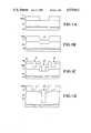
- FIGS. 1a-1kare cross-sections showing a process sequence where silicon dioxide is used as a latent image mask for different types of slots to be formed and in which particularly:
- FIG. 1ais a cross-section of a patterned layer of silicon dioxide which exposes a region in which a slot is to be formed;
- FIG. 1bis a cross-section showing FIG. 1a after additional oxide growth
- FIG. 1cis a cross-sectional view of FIG. 1b after definition by masking of slot regions to be formed and etching of silicon dioxide until it is fully removed in control region 15;
- FIG. 1dis a cross-sectional view of FIG. 1c after etching the first type of slot in region 15';
- FIG. 1eis a cross-section of FIG. 1d after the first type of slot has been filled
- FIG. 1fis a cross-section of FIG. 1e after excess filler material has been removed and a layer of silicon dioxide has been applied;
- FIG. 1gis a cross-section of FIG. 1f after a layer of photoresist has been applied and patterned to expose with a margin the second type of slot region to be formed;
- FIG. 1his a cross-section of FIG. 1g after portions of the overlying silicon dioxide layer have been removed as well as the excess filler material in the second type slot regions to be formed;
- FIG. 1iis a successor cross-section to FIG. 1h after the silicon dioxide above the second slot regions has been fully removed;
- FIG. 1jis a successor cross-section to FIG. 1i after the second type slot regions have been etched in the silicon substrate.
- FIG. 1kis a successor cross-section to FIG. 1j after the second type slots have been filled, the excess filler material has been removed and the oxide mask has been stripped.
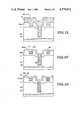
- FIGS. 2a-2iare a series of cross-sectional views showing a process utilizing a dual layer mask wherein the layers have differential etch properties;
- FIG. 2ais a cross-section of a silicon substrate having a first layer of masking material patterned to define a region in which a slot is to be formed;
- FIG. 2bis a successor cross-section to FIG. 2a in which a second mask layer having an etch property different than the property of said first layer has been applied;
- FIG. 2cis a successor cross-section to FIG. 2b in which the second mask layer has been masked and etched to open up a first type slot to be formed and images for second type slots;
- FIG. 2dis a successor cross-section to FIG. 2c after the first type slot has been etched in the silicon substrate;
- FIG. 2eis a successor cross-section to FIG. 2d after the first slot type has been filled with filler material
- FIG. 2fis a successor cross-section to FIG. 2e after excess filler material has been removed;
- FIG. 2gis a successor cross-section to FIG. 2f after the first layer of masking material has been etched to expose the substrate where second type slots are to be formed;
- FIG. 2his a successor cross-section to FIG. 2g after second type slots have been formed and filler material has been universally applied;
- FIG. 2iis a successor cross-section to FIG. 2h after the excess filler material has been removed exposing slots of a first and second type.
- slots of different typesare fabricated using a single latent image mask.
- the slots of different typesare thus located with respect to each other in a self-aligned relationship.
- an oxide of the semiconductor materiale.g. silicon dioxide
- the slots of various typesare defined as latent images in the mask and are fabricated in succession.
- the thickness of the oxide over the substrate regions in which slots of a first type are to be formedis different from the thickness of the oxide over the substrate regions where slots of the second type are to be formed so that substrate regions associated with slots of a particular type may be selectively exposed by a universal etch of known etch rate.
- the slotsare formed they are filled with a suitable material to provide structural integrity for overlying layers.
- a dual layer latent image maskis used in which the two materials have different etch properties. One layer is used as a stop etch layer during fabrication of one of the slot types.
- the purpose of the process of the present inventionis to fabricate slots of various types in self-aligned relationship.
- the slot typewill be determined by the ultimate application, i.e., whether the slot is to be used for purposes of isolation or is to be used as an active element. See, e.g., the co-pending application of R. Bower, "A Bipolar Transistor With Active Elements Formed In Slots", Ser. No. 576,659, filed Feb. 3, 1984.
- a near vertical sidewallis desired or at most a sidewall with no more than several degrees of variation from vertical. If concavities, overhangs or bottle-shapes are present then the slots may be imperfectly filled and contain voids which lead to irregular topographies.
- the depthwill vary based on the intended application. For example, for isolation of memory active elements the slot may only need to be 5 microns deep but for isolation of linear bipolar devices a slot may need to be as deep as 70 microns.
- the widthswill vary in accordance with the quality of the lithographic equipment available to fabricate the integrated circuits. Typical widths will be on the order of several microns to one micron.
- a latent image maskis employed which will harbor the images of all slot types and thereby produce self-alignment for the slot types as they are formed.
- a layer of silicon dioxideis used as a single layer latent image mask. This is designated the Oxide Step Process.
- a dual layer of masking materialsis selected from the group of materials such as silicon nitride, silicon dioxide, organic materials, metals, polycrystalline silicon and other metal oxides.
- one layerserves as the latent image mask to define the slot types to be formed.
- the other layerserves as a stop etch layer to prevent the etching of a second type of slot while the first type of slot is being etched. This is designated the Differential Etch Stop Process.
- FIGS. 1a-1kThe oxide step embodiment of the process of the present invention may be seen with reference to FIGS. 1a-1k.
- the processis shown as implemented in a silicon semiconductor substrate.
- the latent image mask principleapplies to any semiconductor system, e.g., to gallium arsenide, indium phosphide, etc.
- a silicon substrate 10has a layer of silicon dioxide 11 applied thereon.
- the layermay be masked and opened up by conventional lithographic, masking and etching techniques as well as anisotropic etching techniques.
- the regions that are opened upwill establish the areas where a first type of slot is to be formed.
- additional oxideis grown by conventional thermal techniques.
- the layer 11 of silicon dioxide over wafer portions 10is made thicker and a layer 14 forms over step 13.
- a layer of photoresist 12is applied over the silicon dioxide layer 11.
- Photoresist layer 12is patterned and opened up to allow the etching of silicon dioxide layer 11 to define a slot region 15 of a first type and slot regions 16 of a second type. Since the first type slot in substrate region 15 will be formed first, the silicon oxide is completely removed, i.e., is removed down to the exposed surface of silicon substrate 10. Some thickness of silicon dioxide continues to separate the slot region 16 to be formed from the upper surface of silicon substrate 10.
- the end point of the etching processis determined either by knowing the thickness and measuring etch rate and time, or by periodically looking at the color of the layer of silicon dioxide in slot 15 until it disappears. It is desirable to have well controlled etch rates so that the oxide in region 15 can be removed without significant overetching in region 16. Alternately, the end point of etching can be detected by conventional means such as mass spectrometry, trace gas analysis or conductivity should such sophisticated means be available. It is the differential thickness of the oxide layers over regions 15 and 16 that distinguishes slots of the first type from slots of the second type and allows them to be fabricated separately with their own unique specifications.
- the photoresist layer 12is stripped and, as shown in FIG. 1d, the first type slot 15' is etched using a conventional silicon etch.
- the depthwill be determined by the length of etch and will be selected in accordance with the intended application, i.e., isolation, separation or formation of active regions, for which slot region 15 is formed.
- the intended applicationi.e., isolation, separation or formation of active regions, for which slot region 15 is formed.
- a suitable filler materialis deposited over the integrated circuit thereby filling slot 15' as well as all other depressions on the surface including the openings 16 for the second type slots to be formed subsequently.
- the filler materialis selected from classes of conductive and insulating materials and including such materials as silicon nitride, polycrystalline silicon, metal oxides, silicon, etc. The material must readily flow into the slots and preferably isotropically deposits on the surfaces of the slot. The choice of filler material will be based on desired function (isolation versus active device), the size and shape of the slot and on the prospect of avoiding the use of an additional mask.
- the filler materialis etched back by an isotropic etch such as a fluorinated plasma leaving pockets of filler material 18 in the region 16 of silicon dioxide layer 11 over the second type of slots to be formed and a plug 19 in the first type slot region.
- an isotropic etchsuch as a fluorinated plasma leaving pockets of filler material 18 in the region 16 of silicon dioxide layer 11 over the second type of slots to be formed and a plug 19 in the first type slot region.
- this etchbackis one micron or less for a slot that may have a depth of 5 to 70 microns.
- a layer of silicon dioxide 9is universally applied over the exposed surface of the integrated circuit in process, as shown in FIG. 1f.
- a layer of photoresist 8is applied over silicon dioxide 9 and patterned to expose the regions where second type slots are to be formed.
- the exposed regionsare shown in FIG. 1g to be larger than the slot widths in order to ensure that all filler material is removed.
- the exposed portions of silicon dioxide layer 9are etched to expose pockets 18 of filler material.
- the filler materialis etched and a small portion of the upper regions of silicon dioxide layer 11 thereby defining the regions for second type slots will be etched.
- the remaining silicon dioxidehas been etched away.
- the second type slotshave been formed.
- the slot region of the second typeis more shallow than the slot region of the first type.
- slotsmay have varying depths, widths and aspect ratios.
- the second type slotsare filled with a suitable filler material and the surfaces etched back to expose the plug 19 in the first type slot and plugs 24 in the second type slots.
- a planar surfacewill subsequently be produced which will permit the application of overlying layers.
- the second type filler materialcould be the same or of different type than the first type filler material and will be chosen in accordance with the desired application.
- the result of using the unitary latent image maskis that the slots of the first type are arrayed in self-aligned relationship with slots of the second type.
- FIGS. 2a-2iA process which utilizes selective etching to simplify the process sequence for fabricating slots of different types is shown in FIGS. 2a-2i. Fewer mask steps are required if the inherent etch selectivity of one material with respect to another may be employed in order to selectively fabricate one region in lieu of another region. The material with the lowest etch rate can serve as a stop layer while the other layer is being etched through. Thus, dual layers of masking materials having different etch rates are used to fabricate slots of different types. The latent images can still be produced in one of the layers or can be produced in both of the layers. In the embodiment described in the Figures, the latent images of two types of slots are formed in a single masking layer. In FIG.
- a semiconductor substratedescribed for purposes of illustration herein to be a silicon substrate 30, has a layer of a first masking material 31 applied thereon and patterned.
- the exposed region 29defines the location where a slot region of a first type will be formed.
- the first masking layer 31is selected from the class of materials which are compatible with the semiconductor substrate and have an etch property which is different from that of a second masking layer to be applied subsequently.
- Typical materials for layer 31include silicon nitride, silicon dioxide, organic materials and metals.
- a layer of a second masking materialis applied over the first layer 31 and the exposed regions of silicon substrate 30.
- Layer 32will be selected from the same class as layer 31 but will have different etch properties. The differential etch properties of layer 31 with respect to second layer 32 are useful at a later stage in the process to differentiate between slots of the first type and slots of the second type, as shown in FIG. 2d and described subsequently.
- the second masking layer 32is itself masked and defined to produce a latent image 33 of slots of a first type and a latent image 34 of slots of a second type.
- the region 33overlies silicon substrate 30 through the opening in first layer 31 whereas regions 34 of the second slot type overlie solid portions of the masking layer 31.
- layer 31is also resistant to an etch which etches the silicon substrate 30 so that the slot 33' of the first type may be formed, as shown in FIG.
- slot 33'is formed it is filled with a filler material 35 as shown in FIG. 2e.
- the filler materialis selected from the same class of materials described above for the Oxide Step Process.
- the excess filler materialis etched back to a height which defines plug 36 which will permanently reside in the slot region 33'.
- an etchis used which selectively etches through layer 31 but does not significantly etch layer 32.
- the channels 34' over slot regions of the second typeare formed down to the surface of the silicon substrate 30.
- the slot regions 34" of the second typeare formed, as shown in FIG. 2g.
- the etch regions 34" of the second typeare deeper than the etch region 33' of the first type.
- slotsmay have variable depths, widths and aspect ratios.
- the filler material 37which may be the same or different than the other filler material forming plug 36 in the first type slot, is etched back to leave plugs 38 in slot regions 34" of the second type and plug 36 near the surface of slot region 33' of the first type, as shown in FIG. 2i.
- the filler materialmay be nonconducting while for active slots the filler material may be conductive.
- the residual portions of layer 32 and 31may then be removed and a relatively planar surface (not shown) is exposed for subsequent processing. This surface will include veins of exposed portions of plugs 38 and plugs 36 intermixed with residual regions of semiconductor substrate 30.
Landscapes
- Engineering & Computer Science (AREA)
- Physics & Mathematics (AREA)
- Condensed Matter Physics & Semiconductors (AREA)
- General Physics & Mathematics (AREA)
- Manufacturing & Machinery (AREA)
- Computer Hardware Design (AREA)
- Microelectronics & Electronic Packaging (AREA)
- Power Engineering (AREA)
- Chemical & Material Sciences (AREA)
- Crystallography & Structural Chemistry (AREA)
- Drying Of Semiconductors (AREA)
- Element Separation (AREA)
- Local Oxidation Of Silicon (AREA)
- Internal Circuitry In Semiconductor Integrated Circuit Devices (AREA)
- Crystals, And After-Treatments Of Crystals (AREA)
- Bipolar Transistors (AREA)
- Semiconductor Memories (AREA)
- Exposure Of Semiconductors, Excluding Electron Or Ion Beam Exposure (AREA)
Abstract
Description
Claims (24)
Priority Applications (6)
| Application Number | Priority Date | Filing Date | Title |
|---|---|---|---|
| US06/576,658US4579812A (en) | 1984-02-03 | 1984-02-03 | Process for forming slots of different types in self-aligned relationship using a latent image mask |
| JP60500704AJPH0714001B2 (en) | 1984-02-03 | 1985-02-01 | How to form different types of slots in a self-aligned relationship |
| DE3587829TDE3587829T2 (en) | 1984-02-03 | 1985-02-01 | METHOD FOR PRODUCING SELF-ALIGNED TRENCHES WITH USING A MASK. |
| AT85900934TATE105973T1 (en) | 1984-02-03 | 1985-02-01 | METHOD OF MAKING SELF-ALIGNED TRECHES USING A MASK. |
| PCT/US1985/000170WO1985003580A1 (en) | 1984-02-03 | 1985-02-01 | Process for forming slots of different types in self-aligned relationship using a latent image mask |
| EP85900934AEP0172192B1 (en) | 1984-02-03 | 1985-02-01 | Process for forming slots of different types in self-aligned relationship using a mask |
Applications Claiming Priority (1)
| Application Number | Priority Date | Filing Date | Title |
|---|---|---|---|
| US06/576,658US4579812A (en) | 1984-02-03 | 1984-02-03 | Process for forming slots of different types in self-aligned relationship using a latent image mask |
Publications (1)
| Publication Number | Publication Date |
|---|---|
| US4579812Atrue US4579812A (en) | 1986-04-01 |
Family
ID=24305393
Family Applications (1)
| Application Number | Title | Priority Date | Filing Date |
|---|---|---|---|
| US06/576,658Expired - LifetimeUS4579812A (en) | 1984-02-03 | 1984-02-03 | Process for forming slots of different types in self-aligned relationship using a latent image mask |
Country Status (6)
| Country | Link |
|---|---|
| US (1) | US4579812A (en) |
| EP (1) | EP0172192B1 (en) |
| JP (1) | JPH0714001B2 (en) |
| AT (1) | ATE105973T1 (en) |
| DE (1) | DE3587829T2 (en) |
| WO (1) | WO1985003580A1 (en) |
Cited By (27)
| Publication number | Priority date | Publication date | Assignee | Title |
|---|---|---|---|---|
| US4866004A (en)* | 1985-10-05 | 1989-09-12 | Fujitsu Limited | Method of forming groove isolation filled with dielectric for semiconductor device |
| US4895790A (en)* | 1987-09-21 | 1990-01-23 | Massachusetts Institute Of Technology | High-efficiency, multilevel, diffractive optical elements |
| US4911783A (en)* | 1987-04-15 | 1990-03-27 | Bbc Brown Boveri Ag | Process for etching recesses in a silicon substrate |
| US4997746A (en)* | 1988-11-22 | 1991-03-05 | Greco Nancy A | Method of forming conductive lines and studs |
| US5143820A (en)* | 1989-10-31 | 1992-09-01 | International Business Machines Corporation | Method for fabricating high circuit density, self-aligned metal linens to contact windows |
| US5161059A (en)* | 1987-09-21 | 1992-11-03 | Massachusetts Institute Of Technology | High-efficiency, multilevel, diffractive optical elements |
| US5308722A (en)* | 1992-09-24 | 1994-05-03 | Advanced Micro Devices | Voting technique for the manufacture of defect-free printing phase shift lithography |
| US5320932A (en)* | 1990-05-09 | 1994-06-14 | Kabushiki Kaisha Toshiba | Method of forming contact holes |
| US5348828A (en)* | 1990-02-26 | 1994-09-20 | Canon Kabushiki Kaisha | Process for producing electrode substrate |
| US5374503A (en)* | 1992-02-18 | 1994-12-20 | International Business Machines Corporation | Method of forming patterned polyimide films |
| US5429911A (en)* | 1991-03-01 | 1995-07-04 | Teijin Seiki Co., Ltd. | Method of manufacturing a medium having a magnetic pattern |
| US5859469A (en)* | 1997-07-18 | 1999-01-12 | Advanced Micro Devices, Inc. | Use of tungsten filled slots as ground plane in integrated circuit structure |
| US5895253A (en)* | 1997-08-22 | 1999-04-20 | Micron Technology, Inc. | Trench isolation for CMOS devices |
| US5912501A (en)* | 1997-07-18 | 1999-06-15 | Advanced Micro Devices, Inc. | Elimination of radius of curvature effects of p-n junction avalanche breakdown using slots |
| US6011297A (en)* | 1997-07-18 | 2000-01-04 | Advanced Micro Devices,Inc. | Use of multiple slots surrounding base region of a bipolar junction transistor to increase cumulative breakdown voltage |
| US6093641A (en)* | 1997-04-24 | 2000-07-25 | Lg Semicon Co., Ltd. | Method for fabricating semiconductor device with an increased process tolerance |
| US6127276A (en)* | 1998-06-02 | 2000-10-03 | United Microelectronics Corp | Method of formation for a via opening |
| US6175144B1 (en)* | 1998-05-15 | 2001-01-16 | Advanced Micro Devices, Inc. | Advanced isolation structure for high density semiconductor devices |
| US6399449B1 (en)* | 1996-08-09 | 2002-06-04 | Nec Corporation | Semiconductor circuit using trench isolation and method of fabrication a trench isolator |
| US6413835B1 (en)* | 1999-09-17 | 2002-07-02 | Telefonaktiebolaget Lm Ericsson (Publ) | Semiconductor structure and fabrication method of shallow and deep trenches |
| US20040026788A1 (en)* | 2002-08-09 | 2004-02-12 | Kim Deok-Yong | Method for manufacturing a semiconductor wafer |
| US20040056324A1 (en)* | 2002-09-23 | 2004-03-25 | Ning Xian J. | MIM capacitor structures and fabrication methods in dual-damascene structures |
| US20040212086A1 (en)* | 2003-04-28 | 2004-10-28 | Sharp Kabushiki Kaisha | Semiconductor apparatus and production method thereof |
| US6818138B2 (en)* | 2001-06-22 | 2004-11-16 | Hewlett-Packard Development Company, L.P. | Slotted substrate and slotting process |
| US20060040491A1 (en)* | 2004-08-21 | 2006-02-23 | Lim Yeow K | Slot designs in wide metal lines |
| US20060094200A1 (en)* | 2004-10-29 | 2006-05-04 | Leith Steven D | Methods for controlling feature dimensions in crystalline substrates |
| US20120018840A1 (en)* | 2010-07-20 | 2012-01-26 | Yang-Beom Kang | Element isolation structure of semiconductor and method for forming the same |
Families Citing this family (2)
| Publication number | Priority date | Publication date | Assignee | Title |
|---|---|---|---|---|
| US4863560A (en)* | 1988-08-22 | 1989-09-05 | Xerox Corp | Fabrication of silicon structures by single side, multiple step etching process |
| EP0425787A3 (en)* | 1989-10-31 | 1993-04-14 | International Business Machines Corporation | Method for fabricating high circuit density, self-aligned metal lines to contact windows |
Citations (1)
| Publication number | Priority date | Publication date | Assignee | Title |
|---|---|---|---|---|
| US3542551A (en)* | 1968-07-01 | 1970-11-24 | Trw Semiconductors Inc | Method of etching patterns into solid state devices |
Family Cites Families (7)
| Publication number | Priority date | Publication date | Assignee | Title |
|---|---|---|---|---|
| US3479237A (en)* | 1966-04-08 | 1969-11-18 | Bell Telephone Labor Inc | Etch masks on semiconductor surfaces |
| US4139442A (en)* | 1977-09-13 | 1979-02-13 | International Business Machines Corporation | Reactive ion etching method for producing deep dielectric isolation in silicon |
| JPS5626450A (en)* | 1979-08-13 | 1981-03-14 | Hitachi Ltd | Manufacture of semiconductor device |
| JPS5681968A (en)* | 1979-12-07 | 1981-07-04 | Toshiba Corp | Manufacture of semiconductor device |
| JPS59124141A (en)* | 1982-12-28 | 1984-07-18 | Toshiba Corp | Manufacturing method of semiconductor device |
| JPH0665225B2 (en)* | 1984-01-13 | 1994-08-22 | 株式会社東芝 | Method of manufacturing semiconductor memory device |
| US4495025A (en)* | 1984-04-06 | 1985-01-22 | Advanced Micro Devices, Inc. | Process for forming grooves having different depths using a single masking step |
- 1984
- 1984-02-03USUS06/576,658patent/US4579812A/ennot_activeExpired - Lifetime
- 1985
- 1985-02-01DEDE3587829Tpatent/DE3587829T2/ennot_activeExpired - Fee Related
- 1985-02-01EPEP85900934Apatent/EP0172192B1/ennot_activeExpired - Lifetime
- 1985-02-01WOPCT/US1985/000170patent/WO1985003580A1/enactiveIP Right Grant
- 1985-02-01ATAT85900934Tpatent/ATE105973T1/ennot_activeIP Right Cessation
- 1985-02-01JPJP60500704Apatent/JPH0714001B2/ennot_activeExpired - Fee Related
Patent Citations (1)
| Publication number | Priority date | Publication date | Assignee | Title |
|---|---|---|---|---|
| US3542551A (en)* | 1968-07-01 | 1970-11-24 | Trw Semiconductors Inc | Method of etching patterns into solid state devices |
Non-Patent Citations (14)
| Title |
|---|
| Betz et al., "Self-Aligned Contact Holes", IBM Technical Disclosure Bulletin, v. 24, No. 9, Feb. 1982, pp. 4643-4644. |
| Betz et al., Self Aligned Contact Holes , IBM Technical Disclosure Bulletin, v. 24, No. 9, Feb. 1982, pp. 4643 4644.* |
| Ephrath, "Reactive Ion Etching for VLSI", IEEE Transactions on Electron Devices, v. ED-28(11), Nov. 1981, p. 1315-1319. |
| Ephrath, Reactive Ion Etching for VLSI , IEEE Transactions on Electron Devices, v. ED 28(11), Nov. 1981, p. 1315 1319.* |
| Kendall, "Vertical Etching of Silicon at Very High Aspect Ratios", Annual Review of Material Science, vol. 9, 1979, pp. 373-403. |
| Kendall, Vertical Etching of Silicon at Very High Aspect Ratios , Annual Review of Material Science, vol. 9, 1979, pp. 373 403.* |
| Magdo et al., "Self-Aligned ROI to SAM Structure", IBM Technical Disclosure Bull., vol. 24, No. 10, Mar. 1982, pp. 5115-5118. |
| Magdo et al., Self Aligned ROI to SAM Structure , IBM Technical Disclosure Bull., vol. 24, No. 10, Mar. 1982, pp. 5115 5118.* |
| Malaviya, "Self-Aligned Deep Trench Isolation for Bipolar Transistors", IBM Tech. Disclosure Bull., vol. 25(5), Oct. 1982, pp. 2292-2293. |
| Malaviya, Self Aligned Deep Trench Isolation for Bipolar Transistors , IBM Tech. Disclosure Bull., vol. 25(5), Oct. 1982, pp. 2292 2293.* |
| Minegishi et al., "A Submicron CMOS Megabit Level Dynamic RAM Technology Using a DFTC Cell", Proceedings IEDM, 1983, pp. 319-322. |
| Minegishi et al., A Submicron CMOS Megabit Level Dynamic RAM Technology Using a DFTC Cell , Proceedings IEDM, 1983, pp. 319 322.* |
| Wang et al., "Reactive-Ion Etching Eases Restrictions on Materials and Feature Sizes", Electronics, Nov. 1983, pp. 157-161. |
| Wang et al., Reactive Ion Etching Eases Restrictions on Materials and Feature Sizes , Electronics, Nov. 1983, pp. 157 161.* |
Cited By (39)
| Publication number | Priority date | Publication date | Assignee | Title |
|---|---|---|---|---|
| US4866004A (en)* | 1985-10-05 | 1989-09-12 | Fujitsu Limited | Method of forming groove isolation filled with dielectric for semiconductor device |
| US4911783A (en)* | 1987-04-15 | 1990-03-27 | Bbc Brown Boveri Ag | Process for etching recesses in a silicon substrate |
| US5218471A (en)* | 1987-09-21 | 1993-06-08 | Massachusetts Institute Of Technology | High-efficiency, multilevel, diffractive optical elements |
| US4895790A (en)* | 1987-09-21 | 1990-01-23 | Massachusetts Institute Of Technology | High-efficiency, multilevel, diffractive optical elements |
| USRE36352E (en)* | 1987-09-21 | 1999-10-26 | Massachusetts Institute Of Technology | High-efficiency, multilevel, diffractive optical elements |
| US5161059A (en)* | 1987-09-21 | 1992-11-03 | Massachusetts Institute Of Technology | High-efficiency, multilevel, diffractive optical elements |
| US4997746A (en)* | 1988-11-22 | 1991-03-05 | Greco Nancy A | Method of forming conductive lines and studs |
| US5143820A (en)* | 1989-10-31 | 1992-09-01 | International Business Machines Corporation | Method for fabricating high circuit density, self-aligned metal linens to contact windows |
| US5348828A (en)* | 1990-02-26 | 1994-09-20 | Canon Kabushiki Kaisha | Process for producing electrode substrate |
| US5568291A (en)* | 1990-02-26 | 1996-10-22 | Cannon Kabushiki Kaisha | Electrode substrate with light shielding film having upper surface coplanar with upper surface of laminate electrodes |
| US5320932A (en)* | 1990-05-09 | 1994-06-14 | Kabushiki Kaisha Toshiba | Method of forming contact holes |
| US5429911A (en)* | 1991-03-01 | 1995-07-04 | Teijin Seiki Co., Ltd. | Method of manufacturing a medium having a magnetic pattern |
| US5374503A (en)* | 1992-02-18 | 1994-12-20 | International Business Machines Corporation | Method of forming patterned polyimide films |
| US5308722A (en)* | 1992-09-24 | 1994-05-03 | Advanced Micro Devices | Voting technique for the manufacture of defect-free printing phase shift lithography |
| US6399449B1 (en)* | 1996-08-09 | 2002-06-04 | Nec Corporation | Semiconductor circuit using trench isolation and method of fabrication a trench isolator |
| US6093641A (en)* | 1997-04-24 | 2000-07-25 | Lg Semicon Co., Ltd. | Method for fabricating semiconductor device with an increased process tolerance |
| US6011297A (en)* | 1997-07-18 | 2000-01-04 | Advanced Micro Devices,Inc. | Use of multiple slots surrounding base region of a bipolar junction transistor to increase cumulative breakdown voltage |
| US5859469A (en)* | 1997-07-18 | 1999-01-12 | Advanced Micro Devices, Inc. | Use of tungsten filled slots as ground plane in integrated circuit structure |
| US5912501A (en)* | 1997-07-18 | 1999-06-15 | Advanced Micro Devices, Inc. | Elimination of radius of curvature effects of p-n junction avalanche breakdown using slots |
| US5895253A (en)* | 1997-08-22 | 1999-04-20 | Micron Technology, Inc. | Trench isolation for CMOS devices |
| US6365952B1 (en) | 1997-08-22 | 2002-04-02 | Micron Technology, Inc. | Trench isolation for CMOS devices |
| US6175144B1 (en)* | 1998-05-15 | 2001-01-16 | Advanced Micro Devices, Inc. | Advanced isolation structure for high density semiconductor devices |
| US6127276A (en)* | 1998-06-02 | 2000-10-03 | United Microelectronics Corp | Method of formation for a via opening |
| US6413835B1 (en)* | 1999-09-17 | 2002-07-02 | Telefonaktiebolaget Lm Ericsson (Publ) | Semiconductor structure and fabrication method of shallow and deep trenches |
| US6818138B2 (en)* | 2001-06-22 | 2004-11-16 | Hewlett-Packard Development Company, L.P. | Slotted substrate and slotting process |
| US20040026788A1 (en)* | 2002-08-09 | 2004-02-12 | Kim Deok-Yong | Method for manufacturing a semiconductor wafer |
| US6995074B2 (en)* | 2002-08-09 | 2006-02-07 | Samsung Electronics Co., Ltd. | Method for manufacturing a semiconductor wafer |
| WO2004027834A3 (en)* | 2002-09-23 | 2004-07-01 | Ibm | Mim capacitor structures and fabrication methods in dual-damascene structures |
| US6794262B2 (en)* | 2002-09-23 | 2004-09-21 | Infineon Technologies Ag | MIM capacitor structures and fabrication methods in dual-damascene structures |
| US20040056324A1 (en)* | 2002-09-23 | 2004-03-25 | Ning Xian J. | MIM capacitor structures and fabrication methods in dual-damascene structures |
| US20040212086A1 (en)* | 2003-04-28 | 2004-10-28 | Sharp Kabushiki Kaisha | Semiconductor apparatus and production method thereof |
| US20060040491A1 (en)* | 2004-08-21 | 2006-02-23 | Lim Yeow K | Slot designs in wide metal lines |
| US9318378B2 (en)* | 2004-08-21 | 2016-04-19 | Globalfoundries Singapore Pte. Ltd. | Slot designs in wide metal lines |
| US20060094200A1 (en)* | 2004-10-29 | 2006-05-04 | Leith Steven D | Methods for controlling feature dimensions in crystalline substrates |
| US7105456B2 (en) | 2004-10-29 | 2006-09-12 | Hewlett-Packard Development Company, Lp. | Methods for controlling feature dimensions in crystalline substrates |
| US20060264055A1 (en)* | 2004-10-29 | 2006-11-23 | Leith Steven D | Methods for controlling feature dimensions in crystalline substrates |
| US7473649B2 (en) | 2004-10-29 | 2009-01-06 | Steven D Leith | Methods for controlling feature dimensions in crystalline substrates |
| US20120018840A1 (en)* | 2010-07-20 | 2012-01-26 | Yang-Beom Kang | Element isolation structure of semiconductor and method for forming the same |
| US9396985B2 (en)* | 2010-07-20 | 2016-07-19 | Magnachip Semiconductor, Ltd. | Element isolation structure of semiconductor and method for forming the same |
Also Published As
| Publication number | Publication date |
|---|---|
| JPH0714001B2 (en) | 1995-02-15 |
| DE3587829D1 (en) | 1994-06-23 |
| EP0172192A4 (en) | 1989-08-30 |
| JPS61501235A (en) | 1986-06-19 |
| EP0172192B1 (en) | 1994-05-18 |
| EP0172192A1 (en) | 1986-02-26 |
| DE3587829T2 (en) | 1994-11-10 |
| ATE105973T1 (en) | 1994-06-15 |
| WO1985003580A1 (en) | 1985-08-15 |
Similar Documents
| Publication | Publication Date | Title |
|---|---|---|
| US4579812A (en) | Process for forming slots of different types in self-aligned relationship using a latent image mask | |
| US4495025A (en) | Process for forming grooves having different depths using a single masking step | |
| US6033980A (en) | Method of forming submicron contacts and vias in an integrated circuit | |
| US5455194A (en) | Encapsulation method for localized oxidation of silicon with trench isolation | |
| US5880004A (en) | Trench isolation process | |
| US5677237A (en) | Process for removing seams in tungsten plugs | |
| GB2128400A (en) | Isolation and wiring of a semiconductor integrated circuit device and method of manufacturing the same | |
| US6825544B1 (en) | Method for shallow trench isolation and shallow trench isolation structure | |
| US6180517B1 (en) | Method of forming submicron contacts and vias in an integrated circuit | |
| US5747383A (en) | Method for forming conductive lines and stacked vias | |
| JP3214475B2 (en) | Method of forming dual damascene wiring | |
| US4609934A (en) | Semiconductor device having grooves of different depths for improved device isolation | |
| US5231046A (en) | Method for fabricating an interconnection pattern on a BPSG-filled trench isolation structure | |
| JPH08335634A (en) | Method for manufacturing semiconductor device | |
| US6107191A (en) | Method of creating an interconnect in a substrate and semiconductor device employing the same | |
| JP3407023B2 (en) | Method for manufacturing semiconductor device | |
| US5620930A (en) | Trench etching in an integrated-circuit semiconductor device | |
| JPS60226136A (en) | Complementary metal-insulator semiconductor device and its manufacturing method | |
| US5913133A (en) | Method of forming isolation layer for semiconductor device | |
| JPH0729971A (en) | Method for manufacturing semiconductor device | |
| US7537990B2 (en) | Method of manufacturing semiconductor devices | |
| JP3190144B2 (en) | Manufacturing method of semiconductor integrated circuit | |
| US6599825B2 (en) | Method for forming wiring in semiconductor device | |
| JPH023303B2 (en) | ||
| JPH06104334A (en) | Semiconductor device |
Legal Events
| Date | Code | Title | Description |
|---|---|---|---|
| AS | Assignment | Owner name:ADVANCED MICRO DEVICES, INC., 901 THOMPSON PLACE, Free format text:ASSIGNMENT OF ASSIGNORS INTEREST.;ASSIGNOR:BOWER, ROBERT W.;REEL/FRAME:004226/0729 Effective date:19840203 | |
| STCF | Information on status: patent grant | Free format text:PATENTED CASE | |
| FPAY | Fee payment | Year of fee payment:4 | |
| FEPP | Fee payment procedure | Free format text:PAYOR NUMBER ASSIGNED (ORIGINAL EVENT CODE: ASPN); ENTITY STATUS OF PATENT OWNER: LARGE ENTITY | |
| FPAY | Fee payment | Year of fee payment:8 | |
| FPAY | Fee payment | Year of fee payment:12 | |
| AS | Assignment | Owner name:MORGAN STANLEY & CO. INCORPORATED, NEW YORK Free format text:SECURITY INTEREST;ASSIGNOR:LEGERITY, INC.;REEL/FRAME:011601/0539 Effective date:20000804 | |
| AS | Assignment | Owner name:LEGERITY, INC., TEXAS Free format text:ASSIGNMENT OF ASSIGNORS INTEREST;ASSIGNOR:ADVANCED MICRO DEVICES, INC.;REEL/FRAME:011700/0686 Effective date:20000731 | |
| AS | Assignment | Owner name:MORGAN STANLEY & CO. INCORPORATED, AS FACILITY COL Free format text:SECURITY AGREEMENT;ASSIGNORS:LEGERITY, INC.;LEGERITY HOLDINGS, INC.;LEGERITY INTERNATIONAL, INC.;REEL/FRAME:013372/0063 Effective date:20020930 | |
| AS | Assignment | Owner name:SAXON IP ASSETS LLC, TEXAS Free format text:ASSIGNMENT OF ASSIGNORS INTEREST;ASSIGNOR:LEGERITY, INC.;REEL/FRAME:017537/0307 Effective date:20060324 | |
| AS | Assignment | Owner name:LEGERITY HOLDINGS, INC., TEXAS Free format text:RELEASE OF SECURITY INTEREST;ASSIGNOR:MORGAN STANLEY SENIOR FUNDING INC., AS ADMINISTRATIVE AGENT, SUCCESSOR TO MORGAN STANLEY & CO. INCORPORATED, AS FACILITY COLLATERAL AGENT;REEL/FRAME:019699/0854 Effective date:20070727 Owner name:LEGERITY, INC., TEXAS Free format text:RELEASE OF SECURITY INTEREST;ASSIGNOR:MORGAN STANLEY SENIOR FUNDING INC., AS ADMINISTRATIVE AGENT, SUCCESSOR TO MORGAN STANLEY & CO. INCORPORATED;REEL/FRAME:019690/0647 Effective date:20070727 Owner name:LEGERITY INTERNATIONAL, INC., TEXAS Free format text:RELEASE OF SECURITY INTEREST;ASSIGNOR:MORGAN STANLEY SENIOR FUNDING INC., AS ADMINISTRATIVE AGENT, SUCCESSOR TO MORGAN STANLEY & CO. INCORPORATED, AS FACILITY COLLATERAL AGENT;REEL/FRAME:019699/0854 Effective date:20070727 Owner name:LEGERITY, INC., TEXAS Free format text:RELEASE OF SECURITY INTEREST;ASSIGNOR:MORGAN STANLEY SENIOR FUNDING INC., AS ADMINISTRATIVE AGENT, SUCCESSOR TO MORGAN STANLEY & CO. INCORPORATED, AS FACILITY COLLATERAL AGENT;REEL/FRAME:019699/0854 Effective date:20070727 | |
| AS | Assignment | Owner name:SAXON INNOVATIONS, LLC, TEXAS Free format text:ASSIGNMENT OF ASSIGNORS INTEREST;ASSIGNOR:SAXON IP ASSETS, LLC;REEL/FRAME:020156/0053 Effective date:20071016 | |
| AS | Assignment | Owner name:RPX CORPORATION,CALIFORNIA Free format text:ASSIGNMENT OF ASSIGNORS INTEREST;ASSIGNOR:SAXON INNOVATIONS, LLC;REEL/FRAME:024202/0302 Effective date:20100324 |