US4579455A - Photomask inspection apparatus and method with improved defect detection - Google Patents
Photomask inspection apparatus and method with improved defect detectionDownload PDFInfo
- Publication number
- US4579455A US4579455AUS06/492,658US49265883AUS4579455AUS 4579455 AUS4579455 AUS 4579455AUS 49265883 AUS49265883 AUS 49265883AUS 4579455 AUS4579455 AUS 4579455A
- Authority
- US
- United States
- Prior art keywords
- pixel
- matrix
- comparison
- error
- window
- Prior art date
- Legal status (The legal status is an assumption and is not a legal conclusion. Google has not performed a legal analysis and makes no representation as to the accuracy of the status listed.)
- Expired - Lifetime
Links
Images


Classifications
- G—PHYSICS
- G06—COMPUTING OR CALCULATING; COUNTING
- G06T—IMAGE DATA PROCESSING OR GENERATION, IN GENERAL
- G06T7/00—Image analysis
- G06T7/0002—Inspection of images, e.g. flaw detection
- G06T7/0004—Industrial image inspection
- G06T7/001—Industrial image inspection using an image reference approach
- G—PHYSICS
- G03—PHOTOGRAPHY; CINEMATOGRAPHY; ANALOGOUS TECHNIQUES USING WAVES OTHER THAN OPTICAL WAVES; ELECTROGRAPHY; HOLOGRAPHY
- G03F—PHOTOMECHANICAL PRODUCTION OF TEXTURED OR PATTERNED SURFACES, e.g. FOR PRINTING, FOR PROCESSING OF SEMICONDUCTOR DEVICES; MATERIALS THEREFOR; ORIGINALS THEREFOR; APPARATUS SPECIALLY ADAPTED THEREFOR
- G03F1/00—Originals for photomechanical production of textured or patterned surfaces, e.g., masks, photo-masks, reticles; Mask blanks or pellicles therefor; Containers specially adapted therefor; Preparation thereof
- G03F1/68—Preparation processes not covered by groups G03F1/20 - G03F1/50
- G03F1/82—Auxiliary processes, e.g. cleaning or inspecting
- G03F1/84—Inspecting
- G—PHYSICS
- G06—COMPUTING OR CALCULATING; COUNTING
- G06T—IMAGE DATA PROCESSING OR GENERATION, IN GENERAL
- G06T2207/00—Indexing scheme for image analysis or image enhancement
- G06T2207/30—Subject of image; Context of image processing
- G06T2207/30108—Industrial image inspection
- G06T2207/30148—Semiconductor; IC; Wafer
Definitions
- This inventionrelates generally to object inspection apparatus, and relates more particularly to an apparatus and a method for inspecting photomasks having duplicate die patterns thereupon for defects by utilizing an area subtraction technique to identify defects as differences between otherwise duplicate die patterns.
- Photomask inspection systemsthat form pixel images of a photomask to be inspected are known in the prior art.
- Levy patentslisted above, disclose a system that optically projected an image of two die patterns onto photosensitive sensors. The sensors were scanned periodically as the photomask moved to form a two-dimensional pixel representation of the die patterns. These pixel representations were stored in digital form and processed by defect detection circuitry to locate and identify defects.
- One method of processing such two-dimensional pixel representations of die patternswould be to first formulate and store both pixel representations in their entirety in a memory, then to shift the pixel representations to correct for alignment errors, and then to perform a comparison between the two pixel representations to identify regions where they do not match.
- a significant drawback to this methodis the huge memory that would be required for the billions of bits of information necessary to represent die patterns with sufficient precision for state-of-the-art integrated circuits.
- Another method of processing two-dimensional pixel representations of die patterns to determine defectswould use a computer to process the sensor outputs as they are generated by the sensors. While this method would substantially reduce the memory requirements as compared to the method mentioned immediately above, the execution time of the programmed instructions necessary to process the sensor data would be prohibitively lengthy.
- an inspection systemincluding carriage means, illumination means, optical means, detector means, and signal processing means.
- the illumination meansilluminates a photomask to be inspected, while the optical means projects images of two duplicate die patterns of the photomask onto a one-dimensional multi-element detector means.
- the carriage meansmoves the photomask at a constant velocity in a direction normal to the length of the detector means to allow the detector means to sequentially view the entire area to be inspected.
- the detector meansis responsive to the intensity of light incident thereupon and simultaneously generates a plurality of signals that correspond to discrete areas of the photomask and the patterns contained in the images.
- Signal processing meansis provided for processing the signals of the detector means to detect the presence of defects. Included in the signal processing means are pixel memories, a defect detection circuit, timing circuits, a microprocessor, and input and output devices. By periodically scanning the detector means, two-dimensional representations of the die patterns are formed. Digitizers convert the analog signals of the detector means into digital values which are stored temporarily in two pixel memories. Stored at each location in the pixel memories is a pixel value that represents the intensity of light transmitted by a particular area of the photomask.
- Pixel valuesrange from a minimum value which indicates the absence of light impinging upon a sensor and indicates the presence of a pattern feature at the particular area of the photomask, to a maximum value which indicates the full intensity of light impinging upon the sensor and the absence of a pattern feature. Intermediate pixel values indicate a pattern edge within the particular area of the photomask.
- the pixel memorieshold pixel values for only a small number of scans. As the pixel values are shifted through the pixel memories, a defect detector circuit analyzes groups of pixels representing corresponding areas of the two die patterns. Areas of the photomask where defects are indicated by the defect detector circuit are noted and are recorded on magnetic tape or other storage media for later use in photomask visual inspection and repair.
- Defectsare detected by a process of area subtraction between portions of the pixels representing the two die patterns.
- Two square window matrices of seven rows and seven columns of adjacent pixelsare defined for corresponding areas of the two die patterns.
- the center three-by-three matrix of each window matrixis defined as a comparison matrix.
- Each window matrixhas twenty five unique subsets of three-by-three adjacent pixels within its boundaries; one in the center plus twenty-four others that are offset by one or two pixels from the center in one or both directions.
- the process of area subtractioninvolves calculating an error value for each subset of each window matrix.
- the error valueis computed for each subset by summing the squares of the differences between each of the nine pixel values of each subset and the corresonding pixel values of the opposite comparison matrix. If there is no defect and any misalignment between the two representations is less than two pixels in magnitude, at least one error value will be less than a threshold error value. If none of the twenty five error values relating to one comparison matrix are less than the threshold error value, a defect is assumed to be located within that comparison matrix or within the opposite window matrix.
- the magnitude of the threshold error valueis automatically varied according to the number of edges within the window matrices to compensate for errors caused by the different qualitization of edges.
- the present inventiondynamically and accurately inspects the photomask by identifying defects, without requiring two perfectly aligned pixel representations.
- Another advantage of the present inventionis that the sensitivity level of the defect detection circuit is adaptive so as to improve actual defect detection while reducing false defect detection.
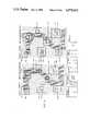
- FIG. 1is a functional block diagram of a photomask inspection apparatus, according to the present invention, for locating and recording areas of non-comparison between duplicate die patterns.
- FIG. 2is an enlarged plan view of two corresponding portions of two die patterns on a photomask to be inspected by the inspection apparatus of FIG. 1.
- FIG. 3is a diagram of a two-dimensional pixel representation of the two die patterns of FIG. 2, with each pixel having a value according to the table at the bottom of FIG. 3.
- FIG. 4is a diagrammatic representation of left and right window and comparison matrices and illustrates pixel labeling nomenclature.
- FIG. 5is a diagrammatic representation of the matrices of FIG. 4 and illustrates misalignment compensation.
- FIG. 6is a diagram of a two-dimensional pixel representation of the two die patterns of FIG. 2 and illustrates the relative positioning of left and right window and comparison matrices.
- FIG. 7is a flow chart that illustrates the operation of the defect detection circuit.
- FIG. 8is a block diagram of the defect detection circuit utilized in the inspection apparatus of FIG. 1.
- FIG. 9is a block diagram of an area subtractor portion of the defect detection circuit of FIG. 8 which determines the existence of a defect within a comparison matrix.
- FIG. 10a, 10b, and 10care diagrammatic representations of the window and comparison matrices at three consecutive points in time.
- FIG. 11is a block diagram of a window matrix latch circuit utilized in the defect detection circuit of FIG. 8.
- FIG. 12is a block diagram of a comparison matrix latch circuit utilized in the defect detection circuit of FIG. 8.
- FIG. 13is a block diagram of a subset difference computation circuit utilized in the defect detection circuit of FIG. 8.
- FIG. 14is a block diagram of a dynamic threshold circuit utilized in the defect detection circuit of FIG. 8.
- the inspection system 20includes an air-bearing stage 22 mounted on a granite table 24 for transporting and positioning a photomask 26 to be inspected.
- the stage 22is movable in the X and Y directions 28 and 30, respectively, by motors that are schematically illustrated at 32 and 34, respectively.
- a photomask holder 36is rotatable in the ⁇ direction by a motor at 38.
- the photomask 26 to be inspectedis mounted on photomask holder 36 which is rotated in the ⁇ direction to align features of the photomask with the X and Y directions.
- Photomask 26is inspected for defects by comparing pixel representations of two duplicate die patterns of the photomask. Defects are identified at those locations where the two pixel representations do not match.
- the pixel representationsare formed by a combination of optical and electronic means.
- the optical meansincludes an illuminator 40, disposed beneath the granite table 24, which illuminates the bottom of photomask 26 through an opening in table 24. Also included are left and right inspection optics 42 and 44, respectively, which project images of light transmitted through the transparent regions of the photomask onto a binocular view head 46, and onto left and right detectors 48 and 50, respectively.
- the binocular view headpermits viewing of a magnified image of the photomask by an operator.
- the task of focusing images of the photomask onto left and right detectors 48 and 50is performed by an automatic focus circuit 52, which responds to the output signals of the detectors.
- Left and right inspection optics 42 and 44are positioned so as to focus identical portions of two die patterns of photomask 26 onto the respective left and right detectors.
- the electronic means for forming pixel representations of the die patternsincludes detectors 48 and 50, which generate analog voltage signals in proportion to the intensity of light impinging thereupon, and left and right digitizers 52 and 54, respectively, which convert the analog voltage signal from the detectors into digital signals.
- the digital signals forming the pixel representations of the die patternsare stored temporarily in left and right pixel memories 56 and 58, respectively.
- the data input to the left pixel memory 56could be taken from a data base 55 which contains an electrically stored replica of the photomask or other object being inspected.
- An example of the use of a data base in a related systemis disclosed in the co-pending U.S. Patent application of Danielson, Wihl, and Joseph, entitled “Reticle Inspection System” Ser. No. 474,461 filed Mar. 11, 1983, and assigned to the assignee of the present application.
- Memories 56 and 58are first-in-first-out (FIFO) type memory circuits that at any one point in time contain only a small fraction of the total pixel representations of the die patterns.
- left and right pixel memories 56 and 58respectively, contain pixel representations for the seven most recent scans of left and right detectors 48 and 50, respectively.
- a system timing control circuit 62provides timing signals to coordinate the sequences of the inspection process. Timing signals and defect results are respectively input to a microprocessor 64 by the system timing control and the defect detector.
- Microprocessor 64controls the position and movement of the air-bearing stage 22 through X, Y, and ⁇ drives 66, 68, and 70, respectively, in response to program instruction and data received from a stage position sensor 72.
- a fine alignment correction circuit 73which responds to data read out of memories 56 and 58 effects fine adjust of left and right pixel data to within plus or minus two pixels.
- 66, 68, and 70are preferably motor controllers and sensor 72 is preferably an optical encoder. Inspection parameters may be prerecorded and input to microprocessor 64 via a tape cassette 74, or may be input manually through manual controls 76. Instructions to the operator or visual display of the photomask may be displayed on a CRT display 78.
- Defect data resulting from the inspection operationis output to the tape cassette.
- the design and operation of those features of the inspection apparatus 20 which are necessary for the formation of the pixel representations of the die patternsare described in U.S. Pat. No. 4,247,203 issued Jan. 27, 1981 to K. Levy and P. Sandland and entitled “Automatic Photomask Inspection System and Apparatus," and U.S. Pat. No. 4,347,001 issued Aug. 31, 1982 K. Levy and P. Sandland and also entitled “Automatic Photomask Inspection Systems and Apparatus,” which are hereby incorporated by reference.
- the microprocessor 64directs the X and Y drives 66 and 68 to move the stage 22 in a serpentine path so that the entire photomask area to be inspected is sequentially viewed by the detectors.
- the inspection operationoccurs during X translations, when the stage 22 is moving at a constant velocity. Between X translations, the stage is indexed in the Y direction to reposition it for the next X translation.
- features on the photomask that are parallel to the X directionare hereinafter referred to as horizontal, and features parallel to the Y direction are hereinafter referred to as vertical.
- the image sensing elements of detectors 48 and 50are preferably photosensors that are responsive to the intensity of light incident thereupon. Photosensors are dispersed at equally spaced positions along a line parallel to the Y direction. The size of the area of the photomask to which each photosensor responds is a function of the magnification of the inspection optics 42 and 44 and the size of the photosensors. At any one time, the photosensors of the left or the right detector view an area of the photomask that is one unit wide in the X direction and is N units long in the Y direction, where N equals the number of photosensors. By moving the stage 22 in the X direction at a constant velocity and by periodically scanning the analog output signals of the photosensors, a two-dimension representation of the photomask is formed.
- the digitized sensor outputs for each scanare stored temporarily in the left and right pixel memories 56 and 58 to form the pixel representations of the die patterns.
- Each scan of the N photosensors of each detectordefines one vertical column of each pixel representation.
- a pixelis the rectangularly shaped element of which the pixel representations are composed.
- Each pixelcorresponds to a small rectangular area of the photomask.
- the Y dimension of each pixelis determined by the photosensor spacing and the optical magnification, while the X dimension is determined by the stage velocity in X and the frequency of scanning the outputs of the photosensors.
- Each pixelhas an X and Y address corresponding to the X and Y coordinate location of the small rectangular area of the photomask that is viewed by its photosensor during the point in time when the photosensor output is scanned.
- Each pixelhas an associated pixel value that is proportional to the intensity of light incident upon its photosensor during the point in time when the photosensor output is scanned.
- the analog output signals of the photosensorsare digitized by digitizers 48 and 50 to one of four values: 3 (white), 2 (white-grey), 1 (black-grey), and 0 (black).
- Whiteindicates that the photomask area imaged on the photosensor is transparent, which allows the full intensity of the illumination light to impinge upon the photosensor.
- Blackindicates that an opaque area of the pattern completely blocks illumination light from reaching the photosensor.
- White-grey and black-greyindicate the presence of both transparent and opaque patterns within the area imaged on the photosensor, caused by the presence of one or more edges.
- a white-grey pixel valueindicates that the photomask area that is imaged on the photosensor contains more transparent area than opaque area.
- a black-grey pixel valueindicates more opaque area than transparent area in the photomask area imaged on the photosensor.
- Defect detection by the inspection apparatus 20involves the comparison of two duplicate die patterns. Defects are indicated in those areas where the die patterns do not match.
- a left pattern 80 and a right pattern 82are portions of duplicate die patterns, and have opaque regions on an otherwise transparent plate forming the photomask 26.
- FIG. 3Complete two-dimensional pixel representations of left and right patterns 80 and 82 are shown in FIG. 3.
- Each pixel of the left and right pixel representations 98 and 100, respectively,has a pixel value as indicated by the symbol table of FIG. 3.
- Pixels 94 and 96, for example, bothare white and have a value of 3, since both represent transparent areas of the left and right patterns.
- the pixel representations shown in FIG. 3do not actually exist at any one time in the left and right pixel memories 56 and 58, since only pixel values from the seven most recent scans of the detectors 48 and 50 are stored. Rather, the pixel representations shown are composites of the digitized output signals of forty photosensors of the left detector 48 and forty photosensors of the right detector 50 during twenty-seven consecutive scans.
- the defects in the right pattern 82are indicated in the right pixel representation 100 as irregularities in pixel values as compared to the left pixel representation 98.
- Spot 84is indicated by a black pixel 102 within a field of white pixels.
- Spot 86is indicated by several adjacent black, black-grey, and white grey pixels 104 within a field of white pixels.
- Void 88is indicated by white, white-grey, and black-grey pixels 106 within a field of black pixels.
- Gap 90is indicated in the right pixel representation as a horizontal line of white pixels 108 across the diagonal feature formed by black pixels.
- Protrusion 92is indicated by two black pixels 110 that extend from an otherwise black-grey edge.
- pixel dimensionsare on the order of one half micrometer to permit inspection of photomask geometries on the order of one and one-half micrometer. Vibration of the stage 22 and the objectives 42 and 44, and the die-to-die registration on the photomask as well as line width variations prohibit, as a practical matter, perfect alignment between pixel representations.
- FIG. 3An example of a quantization error is shown in equivalently positioned pixels 112 and 114 in the left and right pixel representations 98 and 100 (FIG. 3).
- a vertical edge of the left pattern 80is so positioned that it falls between pixel 112 and pixel 116, with the result that pixel 112 is black and pixel 116 is white.
- the vertical edgefalls within pixel 114, so its value is white-grey.
- Residual alignment errors of plus or minus two pixelsmay also occur where no defect is indicated.
- the die patternis shifted downward relative to the left pixel representation by a distance slightly greater than one pixel.
- the lower horizontal edge of the left pixel representationis between pixels 118 and 120, while the lower horizontal edge of the right pixel representation is in pixel 128.
- a pixel to pixel comparison between the equivalently positioned pixels 118 and 124, 120 and 126, 122 and 128would show disagreements between pixels 120 and 126, and between pixels 122 and 128, even though no defect is present. It is necessary, therefore, to provide means for compensating for such misalignment between pixel representations.
- Defect detector 60compensates for alignment errors of up to two pixels in either or both the X and Y directions 28 and 30, while detecting defects by a comparison of equivalently positioned pixels.
- Left and right comparison matricesare defined as square matrices of adjacent pixels in three rows and three columns. The pixels of the left and right comparison matrices are equivalently positioned within the left and right pixel representations, that is they would be identical if the left and right pixel representations were perfectly aligned.
- Left and right window matricesare defined as square matrices of adjacent pixels in seven rows and seven columns having the left and right comparison matrices at the respective centers thereof.
- FIG. 4also illustrates the nomenclature used below in reference to the pixels of the window and comparison matrices. Pixels are referred to as L or R (indicating left or right representation), column number, and row number.
- the comparison matricesare located at the intersection of columns 3, 4, and 5 and rows 3, 4, and 5.
- the defect detector circuit 60compares each comparison matrix to all of the possible subsets of the opposite window matrix that are equal in size to the comparison matrix.
- Each window matrixhas twenty-five unique subsets of adjacent pixels in three rows and three columns.
- One such subset of the left window matrix 130is the left comparison matrix 132.
- Other subsetsare shifted relative to the comparison matrix by either one or two pixels in either or both the X and Y directions.
- the subset containing pixels L(1;1), L(1;2), L(1;3), L(2;1), L(2;2), L(2;3), L(3;1), L(3;2), and L(3;3)is shifted two pixels in the +X direction and two pixels in the +Y direction from the center of the window matrix.
- the defect detector circuitcompensates for alignment errors of up to two pixels in either or both the X or Y directions. If there were no quantization errors, then one of the twenty-five comparisons between the comparison matrix of one side and the subsets of the window matrix of the opposite side will yield an exact match, unless a defect is present within the comparison matrix.
- the right comparison matrix 136 and a subset 140 of the left window matrix 130there is an exact match between the right comparison matrix 136 and a subset 140 of the left window matrix 130.
- the right pixel representationis offset relative to the left pixel representation by two pixels in the +X direction and one pixel in the -Y direction.
- error threshold valuesare utilized in the comparison process.
- the defect detector circuit 60computes an error value for each of the twenty-five comparisons between a comparison matrix and the subsets of the opposite window matrix. Then it compares each error value to an error threshold value, and if at least one error value is less than the error threshold value, no defect is indicated. By setting the error threshold value to a non-zero value, edge quantization effects are compensated for.
- an error valueis computed for each of the twenty-five comparisons between a comparison matrix and the subsets of the opposite window matrix.
- One method of computing the error valueis to sum the absolute values of the differences in pixel value between each pixel of the comparison matrix and the corresponding pixel of the subset.
- the magnitude of the error value computed according to this methodis proportional to the number of pixels that disagree in value and is also proportional to the magnitude of the disagreement.
- the preferable method of error value computationcomputes an error value by summing the squares of the differences between the pixel values of each pixel of the comparison matrix and its corresponding pixel of the subset.
- the error value for the comparison between the right comparison matrix and the lower right subset of the left window matrixis as follows: [L(1;1)-R(3;3)] 2 +[L(1;2)-R(3;4)] 2 +[L(1;3)-R(3;5)] 2 +[L(2;1)-R(4;3)] 2 +[L(2;2)-R(4;4)] 2 +[L(2;3)-R(4;5)] 2 +[L(3;1)-R(5;3)] 2 +[L(3;2)-R(5;4)] 2 +[L(3;3)-R(5;5)] 2 .
- An advantage to this alternative methodis that edge quantization effects which tend to be small are less heavily weighted than are errors due to defects.
- Edge quantization effectsare manifested in the pixel representations by variations in the pixel values at edges of the die patterns. This is determined by where the edge strikes the sampling grid.
- An edge in one pixel representationmay be represented, for example, by a row of pixels that are black, black, and white.
- the sampling and quantization processcan, however, cause the same edge of the opposite pattern to be represented by a row of pixels that are black, black-grey, and white.
- the contribution of the edge effect to the error valueis equal to the square of the difference in pixel values, (1-0) 2 , which equals one.
- the error value of this comparisonis equal to three.
- the error threshold valueis equal to three when one edge is within the window matrix. If, however, the minimum size of the geometry of the die patterns is not greater than the width of two pixels, then two edges could be present within a comparison matrix. It has been found that an error threshold value of six will compensate for quantization errors in such a case.
- the error threshold valueis preferably equal to eight when one vertical and one horizontal edge are within a window matrix.
- the defect detector circuit 60adjusts the error threshold value to zero when no edges exist in a window matrix. This increases defect detection sensitivity since a defect that causes a minimum error value of one or more will be detected.
- a right window matrix 142has one black pixel 144 that represents spot 84 (FIG. 2).
- spot 84does not cause a defect to be detected in the left pixel representation, even though the left and right pixel representations do not match.
- To determine whether a defect exists within the left comparison matrix 150it is compared to all twenty-five subsets of the right window matrix 142. Although nine of the subsets contain the black pixel 144 and do not match with the left comparison matrix, the remaining sixteen subsets do match. Since there is a match between the left comparison matrix 150 and at least one subset of the right window matrix 142, no defect is detected.
- Right comparison matrix 152is compared against all subsets of its corresponding left window 154. No subsets of the left window matrix 154 exactly matches the pixel values of the right comparison matrix.
- the minimum error valueis found at any of the five subsets in rows 1, 2, and 3.
- R(3;3)is black-grey and contributes a value of one to the error value.
- R(5;3)is white-grey and contributes a value of four.
- R(3;4)is white-grey and contributes a value of one.
- R(4;4)is black and contributes a value of nine.
- R(4;3), R(5;4), R(3;5), R(4;5), and R(5;5)all match their corresponding subset pixel values and contribute zero.
- the minimum error value of right comparison matrix 152is therefore equal to fifteen.
- Left window matrix 154has one horizontal line therein, so the error threshold value is equal to six. Clearly the minimum error value of the right comparison matrix 152 exceeds the error threshold value, thus indicating a defect within matrix 152.
- the left window matrix 154has an edge therein, the corresponding right window matrix 156 does not, however the defect has created vertical and horizontal edges so the threshold is set to eight. Even so, no defect is indicated within the left comparison matrix 158 because it matches exactly with several subsets of the right window matrix 156.
- protrusion 92is detected as a defect within right comparison matrix 160.
- the minimum error value found in comparing the right comparison matrix 160 to the twenty-five subsets of its corresponding left window matrix 162is equal to eleven, which clearly exceeds the error threshold value for one edge and indicates a defect.
- the presence of a defect caused by void 88is detected within right comparison matrix 164.
- the minimum error valueis equal to twenty-three. Since the lower left pixel of the left window matrix, L(7;1), is white-grey, there is a corner within the left window matrix. Accordingly, the error threshold value for the left window matrix is equal to eight. The minimum error value of the right comparison matrix 164 is far in excess of the error threshold value, thus indicating the defect.
- the defect caused by gap 90is detected within right comparison matrix 168 when it is compared to the subsets of its corresponding left window matrix 170.
- the minimum error value from the comparisonis found to be twenty-seven, again exceeding the error threshold value of eight and indicating a defect within the right comparison matrix.
- the right comparison matrix 172has three rows of pixels with values of black, white-grey, and white, indicating a vertical edge within column four.
- the corresponding left comparison matrix 174has three rows of pixels with values of black, black, and white, indicating a corresponding vertical edge between columns three and four. Comparing the right comparison matrix to the subsets in columns two, three, and four of the left window matrix 176, yields a minimum error value of three, and thus no defect. Comparing the left comparison matrix to the subsets in columns four, five, and six of the right window matrix 178, also yields a minimum error value of three and, therefore, no defect is indicated.
- the upper left corner of the patternis an example of an edge effect causing a minimum error value equal to eight in the absence of any defects.
- the edges of the cornerare represented within the left window matrix 180 as sharp black to white transitions. Within the right window matrix 182, however, the edges are black-grey with a white-grey corner pixel.
- the minimum error value found in the comparison of the left comparison matrix 184 to the subsets of the right window matrix 182is equal to three.
- the comparison of the right comparison matrix 186 to the subsets of the left window matrix 180yields a minumum error value of eight, since pixels R(5;3), R(5;4), R(4;5) and R(3;5) have contributions of one and pixel R(5;5) has a contribution of four.
- the pixel representations shown in FIGS. 3 and 6do not actually exist at any one time in the left and right pixel memories 56 and 58, since only pixel values from the seven most recent scans of the detectors 48 and 50 are stored. Defect detection is continuously performed by the defect detector circuit 60 on the pixel representations of the seven most recent scans of the output signals of left and right detectors 48 and 50.
- Each pulse of a pixel clockadvances the left and right comparison and window matrices by one row of pixels in the +Y direction.
- the defect detectordetermines whether a defect exists within either the left or the right comparison matrix. This process continues throughout each scan until the window matrices reach the +Y limit of the pixel representations.
- a new scanis then begun with the oldest scan line dropped off and the newest added; the comparison and window matrices are repositioned at the top of the pixel representations.
- Each pixelis utilized in the defect calculations a total of forty-nine times, during seven consecutive scans.
- Each pixelis utilized as a comparison pixel a total of nine times, during the middle three of the seven consecutive scans.
- FIG. 7is a flow chart that generally illustrates the operation of the defect detection circuit 60.
- the left and right window matricesare updated at 188.
- error threshold values, ET l and ET rare computed for the left and right window matrices at 190.
- ET l and ET rare functions of the number of horizontal and vertical edges within their respective window matrices.
- the next step, at 192,is to compute the error values, D l , of the right comparison matrix with each of the twenty-five subsets of the left window matrix and the error values, D r , of the left comparison matrix with each of the twenty-five subsets of the right window matrix.
- Each error valueis equal to the sum of the squares of the differences between each of the nine corresponding pairs of pixels.
- the next step, at 194,is to compare each of the twenty-five D l values to ET l , and if none are less than ET l , then a defect exists. It is not always possible to determine which side is defective.
- the twenty-five D r valuesare compared to ET r , and if none are less than ET r , then a defect exists.
- the pixel clockpulses once again, returning execution to the top of the flow chart.
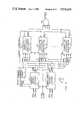
- FIGS. 8, 9, 11, 12, 13, and 14describe the implementation of the defect detector 60 in detail.
- FIG. 8illustrates the division of the defect detector circuit into a first area subtractor subsystem 198 for detecting defects in the right comparison matrix, and a second area subtractor subsystem 200 for detecting defects in the left comparison matrix.
- a first area subtractor subsystem 198for detecting defects in the right comparison matrix
- a second area subtractor subsystem 200for detecting defects in the left comparison matrix.
- MSBmost significant bit
- LSBleast significant bit
- OR gate 202indicates a defect to the microprocessor 64.
- FIG. 9illustrates the circuit of the first and second area subtractor subsystems 198 and 200. Both area subtractor circuits are identical with the exception of the source of the pixel value data. During each period of the pixel clock, the area subtractor circuits 198 and 200 perform the functions listed in the flow chart of FIG. 7. Each area subtractor circuit computes an error threshold value according to the number of edges in the appropriate window matrix, computes error values for each subset of the window matrix in comparison to the opposite comparison matrix, and indicates the existence of a defect if all error values exceed the error threshold value.
- Each area subtractor circuitincludes window matrix latches 204 for temporarily storing pixel values of the window matrix, comparison matrix latches 206 for temporarily storing pixel values of the opposite comparison matrix, dynamic threshold circuit 208 for determining the magnitude of the error threshold value as a function of the number of horizontal and vertical edges within the window matrix, subset difference computation circuits 210, 212, and 214 for calculating error values for each subset with respect to the comparison matrix and for comparing the error values to the error threshold value, and an AND gate 216 for summing the results of the difference computation circuits.
- the subset difference computation circuitsare twenty-five in number, and are wired in parallel to permit simultaneous error computation in all twenty-five subsets.
- Window matrix latches 204, comparison matrix latches 206, subset difference computation circuits 210, 212, and 214, and dynamic threshold circuit 208are all described below in greater detail in relation to FIGS. 11, 12, 13, and 14, respectively.
- FIG. 10illustrates the method utilized to temporarily store the pixel values of a window matrix and a comparison matrix.
- the latches 204 of the window matrixare operable for storing seven columns and five rows of pixels.
- the latches 206 of the comparison matrixare operable for storing three columns and three rows of pixels.
- the window matrix latches 204clears the pixel values of row five, sequentially shifts the pixels of row four to row five, the pixels of row three to row four, the pixels of row two to row three, the pixels of row one to row two, and loads seven new pixel values from one pixel memory into row one.
- the comparison matrix latches 206clears the pixel values of its row three, shifts the pixels of row two to row three and the pixels of row one to row two, and loads three new pixel values from the other pixel memory into row one.
- the three pixels loaded into row one of the comparison matrix latchesare positioned in columns three, four, and five of its companion window matrix. Conversely, the pixels in columns three, four, and five and in row one of the window matrix latches are simultaneously loaded into the comparison matrix latches of the opposite area subtractor circuit.
- FIG. 10illustrates the window matrix latches 204 and the comparison matrix latches 206 at three consecutive points in time.
- the latchesare as shown in FIG. 10a.
- row five of the window matrix at t 0has been shifted out and is located at 218, shown in FIG. 10b in phantom lines as row six.
- row three of the comparison matrix at t 0has been shifted out and is located at 220, shown in phantom lines as row four.
- row five of the window matrix at t 1has been shifted out and is located at 222, shown in phantom lines as row six, and row six at t 1 is shown at 224 in phanton lines as row seven.
- row three of the comparison matrix at t 1has been shifted out and is located at 226, shown in phantom lines as row four, and row four at t 1 is shown at 228 in phantom lines as row five.
- the previously described seven by seven window matrixis represented at t 2 by the five rows of the window matrix latches 204, plus the phantom rows six and seven.
- the previously described three by three comparison matrixis represented at t 2 by row three of the comparison matrix latches 206, plus the phantom rows four and five. Note that the phantom row seven of the window matrix is equal to row five of the window matrix latches at t 0 and that the phantom row is six is equal to row five of the window matrix latches at t 1 .
- the phantom row five of the comparison matrix at t 2is equal to row three of the comparison matrix latches at t 0 and that the phantom row four at t 2 is equal to row three of the comparison matrix latches at t 1 .
- this error valueis identically equal to: [W(1;5)-C(3;3)] 2 at t 0 +[W(2;5)-C(4;3)] 2 at t 0 +[W(3;5)-C(5;3] 2 at t 0 +[W(1;5)-C(3;3)] 2 at t 1 +[W(2;5)-C(4;3)] 2 at t 1 +[W(3;5)-C(5;3)] 2 at t 1 +[W(1;5)-C(3;3)] 2 at t 2 +[W(2;5)-C(4;3)] 2 at t 2 +[W(3;5)-C(5;3)] 2 at t 2 .
- the error values of the three by three subsets of the window matrixmay be calculated. Therefore, the inputs to the twenty-five subset difference computation circuits 210, 212, and 214 (FIG. 9) are the two bit values of the three pixels in row three of the comparison matrix latches 206 and the two bit values of the three pixels of each of the twenty-five combinations of three horizontally adjacent pixels within the window matrix latches 204.
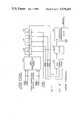
- FIG. 11illustrates the interconnection of the five latches 230, 232, 234, 236, and 238 of the window matrix latches 204.
- Latch 230receives, from a corresponding pixel memory, the seven most significant bits (MSB) and the seven least significant bits (LSB) representing the seven pixels of row one.
- MSBmost significant bits
- LSBleast significant bits
- the pixel values of row oneare input to latch 232 and to five subset difference computation circuits via bus 240.
- the outputs of latch 232are input to latch 234 and to five additional subset difference computation circuits via bus 240.
- the most significant bits of the outputs of latches 230 and 232are input to the dynamic threshold circuit 208 and are used to determine the presence of edges within the window matrix.
- Latches 234, 236, and 238are cascaded together and are also connected to the subset difference computation circuits via bus 240.
- FIG. 12illustrates the interconnections of latches 242, 244, and 246 that form the comparison matrix latches 206.
- Latch 242receives, from the opposite pixel memory, the three most significant bits and the three least significant bits representing row one pixels in columns three, four, and five.
- Latches 242, 244, and 246are cascaded together such that the pixel values transfer to latch 244 and then to latch 246 upon pulses of the pixel clock.
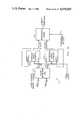
- FIG. 13the circuitry of a representative subset difference computation circuit 210.
- Three MSB and three LSB for three horizontally adjacent pixels of the window matrix plus three MSB and three LSB for the row three pixels of the comparison matrixform twelve address lines for a row subtractor PROM 248.
- Stored at the 212 memory cells of PROM 248are the results of the preliminary error calculation described above: [W(1)-C(1)] 2 +[W(2)-C(2)] 2 +[W(3)-C(3)] 2 .
- the implementation of this calculation in a PROM deviceis advantageous in reducing the amount of circuitry and improving the speed of circuit 210.
- the output of the row subtractor PROM 248is input to a t 2 latch 250, which is cascaded with a t 1 latch 252 and a t 0 latch 254.
- the preliminary error calculation resultsare shifted between latches 250, 252, and 254.
- the preliminary error calculation results of three consecutive time periods that are stored in latches 250, 252, and 254are input to a row summer PROM 256.
- the values stored in latches 250, 252, and 254act as addresses to access memory cells of the row summer PROM 256.
- Stored in the memory cells of PROM 256are error values that are equal to the sums of the preliminary error calculation results.
- PROM 256is operable for summing the three preliminary error results stored in latches 250, 252, and 254.
- the output of PROM 256is stored in latch 258 and is compared to the error threshold value by a threshold comparator 260. If the error value thus calculated is less than or equal to the error threshold value, a match (no defect) is indicated.
- the magnitude of the error threshold valueis determined by the dynamic threshold circuit illustrated in FIG. 14.
- the most significant bits (MSB) from the fourteen pixels in rows one and two of the window matrix latches 204are input to an edge detector PAL (programmable array logic) 262.
- the PALis programmed to return a logic high value on a vertical edge output port 264 if there is a vertical edge within rows one and two, and to return a logic high value on a horizontal edge output port 266 if there is a horizontal edge within rows one and two.
- a vertical edgeis indicated if any two horizontally adjacent pixels are different in value.
- a horizontal edgeis indicated if any two vertically adjacent pixels are different in value.
- Two down counters 268 and 270are utilized to count down from seven once an edge is found. The outputs of counters 268 and 270 are fed back to count enable inputs to prevent the counters from passing zero.
- Outputs from the down counters 268 and 270indicate whether there is a vertical or horizontal edge within the window matrix. These outputs serve as address inputs to a threshold PROM 272 to determine the error threshold value. In addition, an operator may direct the threshold PROM through a threshold select line 274 to select a certain error threshold value.
- the present inventionhas been described above in terms of a preferred embodiment specifically designed to detect defects in photomasks, it will be understood that the apparatus or various parts thereof could be adapted for other applications.
- the source of one of the pixel representationsmay be a stored database, rather than an optically and electronically measured die pattern.
- the inventioncould be used to inspect metal masks and reticles. Alterations and modifications may be made to the disclosed embodiment without departing from the inventive concept thereof.
- the window matricesmay be eight by eight pixels and the comparison matrices may be four by four pixels, without departing from the inventive concept.
- the pixel valuesmay be four bit binary numbers (or any other number) instead of two bit, also without departing from the inventive concept. Accordingly, it is Applicants' intent that the appended claims be interpreted as covering all such alterations, modifications, or other applications as fall within the true scope of the invention.
Landscapes
- Engineering & Computer Science (AREA)
- Physics & Mathematics (AREA)
- General Physics & Mathematics (AREA)
- Quality & Reliability (AREA)
- Computer Vision & Pattern Recognition (AREA)
- Theoretical Computer Science (AREA)
- Investigating Materials By The Use Of Optical Means Adapted For Particular Applications (AREA)
Abstract
Description
Claims (17)
Priority Applications (3)
| Application Number | Priority Date | Filing Date | Title |
|---|---|---|---|
| US06/492,658US4579455A (en) | 1983-05-09 | 1983-05-09 | Photomask inspection apparatus and method with improved defect detection |
| GB848411785AGB8411785D0 (en) | 1983-05-09 | 1984-05-09 | Photomask inspection apparatus |
| GB848411786AGB8411786D0 (en) | 1983-05-09 | 1984-05-09 | Photomask inspection apparatus |
Applications Claiming Priority (1)
| Application Number | Priority Date | Filing Date | Title |
|---|---|---|---|
| US06/492,658US4579455A (en) | 1983-05-09 | 1983-05-09 | Photomask inspection apparatus and method with improved defect detection |
Publications (1)
| Publication Number | Publication Date |
|---|---|
| US4579455Atrue US4579455A (en) | 1986-04-01 |
Family
ID=23957111
Family Applications (1)
| Application Number | Title | Priority Date | Filing Date |
|---|---|---|---|
| US06/492,658Expired - LifetimeUS4579455A (en) | 1983-05-09 | 1983-05-09 | Photomask inspection apparatus and method with improved defect detection |
Country Status (2)
| Country | Link |
|---|---|
| US (1) | US4579455A (en) |
| GB (2) | GB8411785D0 (en) |
Cited By (143)
| Publication number | Priority date | Publication date | Assignee | Title |
|---|---|---|---|---|
| US4737920A (en)* | 1983-11-30 | 1988-04-12 | Nippon Kogaku K. K. | Method and apparatus for correcting rotational errors during inspection of reticles and masks |
| US4791586A (en)* | 1984-12-26 | 1988-12-13 | Hitachi, Ltd. | Method of and apparatus for checking geometry of multi-layer patterns for IC structures |
| US4845558A (en)* | 1987-12-03 | 1989-07-04 | Kla Instruments Corporation | Method and apparatus for detecting defects in repeated microminiature patterns |
| US4851902A (en)* | 1986-10-29 | 1989-07-25 | Electroplating Engineers Of Japan, Limited | Auatomatic inspection system for IC lead frames and visual inspection method thereof |
| US4876727A (en)* | 1986-02-10 | 1989-10-24 | Nukem Gmbh | Method and apparatus for detecting faults in an object |
| EP0225651A3 (en)* | 1985-12-13 | 1990-01-10 | Dainippon Screen Mfg. Co., Ltd. | Method of and apparatus for detecting pattern defects |
| US4898471A (en)* | 1987-06-18 | 1990-02-06 | Tencor Instruments | Particle detection on patterned wafers and the like |
| EP0254644A3 (en)* | 1986-07-22 | 1990-07-18 | Schlumberger Technologies, Inc. | Mask alignment and measurement of critical dimensions in integrated circuits |
| US4949390A (en)* | 1987-04-16 | 1990-08-14 | Applied Vision Systems, Inc. | Interconnect verification using serial neighborhood processors |
| US4991007A (en)* | 1989-05-05 | 1991-02-05 | Corley Ferrand D E | Image evaluation of at least one characteristic of an object, and method of evaluation |
| US5109430A (en)* | 1986-07-22 | 1992-04-28 | Schlumberger Technologies, Inc. | Mask alignment and measurement of critical dimensions in integrated circuits |
| US5125040A (en)* | 1983-06-23 | 1992-06-23 | Fujitsu Ltd. | Inspection method of photomask reticle for semiconductor device fabrication |
| US5127737A (en)* | 1989-01-13 | 1992-07-07 | G. D. Societa Per Azioni | Cigarette end group inspection system |
| US5181081A (en)* | 1990-09-06 | 1993-01-19 | Wea Manufacturing, Inc. | Print scanner |
| US5247585A (en)* | 1988-12-28 | 1993-09-21 | Masaharu Watanabe | Object recognition device |
| EP0573345A1 (en)* | 1992-06-03 | 1993-12-08 | Commissariat A L'energie Atomique | Data stream comparison process and device for carrying out the method |
| US5432600A (en)* | 1992-05-15 | 1995-07-11 | Philip Morris Incorporated | Systems for optically inspecting cylindrical surfaces |
| US5448365A (en)* | 1992-05-15 | 1995-09-05 | Philip Morris Incorporated | Systems for optical inspection |
| US5539752A (en)* | 1995-06-30 | 1996-07-23 | Advanced Micro Devices, Inc. | Method and system for automated analysis of semiconductor defect data |
| US5553168A (en)* | 1994-01-21 | 1996-09-03 | Texas Instruments Incorporated | System and method for recognizing visual indicia |
| US5563702A (en)* | 1991-08-22 | 1996-10-08 | Kla Instruments Corporation | Automated photomask inspection apparatus and method |
| US5572598A (en)* | 1991-08-22 | 1996-11-05 | Kla Instruments Corporation | Automated photomask inspection apparatus |
| US5586058A (en)* | 1990-12-04 | 1996-12-17 | Orbot Instruments Ltd. | Apparatus and method for inspection of a patterned object by comparison thereof to a reference |
| US5619588A (en)* | 1992-07-27 | 1997-04-08 | Orbot Instruments Ltd. | Apparatus and method for comparing and aligning two digital representations of an image |
| US5619429A (en)* | 1990-12-04 | 1997-04-08 | Orbot Instruments Ltd. | Apparatus and method for inspection of a patterned object by comparison thereof to a reference |
| US5649169A (en)* | 1995-06-20 | 1997-07-15 | Advanced Micro Devices, Inc. | Method and system for declustering semiconductor defect data |
| US5767974A (en)* | 1995-02-24 | 1998-06-16 | Mitsubishi Denki Kabushiki Kaisha | Apparatus and method for identifying photomask pattern defects |
| US5777901A (en)* | 1995-09-29 | 1998-07-07 | Advanced Micro Devices, Inc. | Method and system for automated die yield prediction in semiconductor manufacturing |
| US5825482A (en)* | 1995-09-29 | 1998-10-20 | Kla-Tencor Corporation | Surface inspection system with misregistration error correction and adaptive illumination |
| US5864394A (en)* | 1994-06-20 | 1999-01-26 | Kla-Tencor Corporation | Surface inspection system |
| US5913105A (en)* | 1995-11-29 | 1999-06-15 | Advanced Micro Devices Inc | Method and system for recognizing scratch patterns on semiconductor wafers |
| US5917588A (en)* | 1996-11-04 | 1999-06-29 | Kla-Tencor Corporation | Automated specimen inspection system for and method of distinguishing features or anomalies under either bright field or dark field illumination |
| US5923430A (en)* | 1993-06-17 | 1999-07-13 | Ultrapointe Corporation | Method for characterizing defects on semiconductor wafers |
| US5963314A (en)* | 1993-06-17 | 1999-10-05 | Ultrapointe Corporation | Laser imaging system for inspection and analysis of sub-micron particles |
| US5967676A (en)* | 1998-03-31 | 1999-10-19 | Microtech Conversion Systems, Inc. | Image orientation system for disk printing |
| US6040912A (en)* | 1998-09-30 | 2000-03-21 | Advanced Micro Devices, Inc. | Method and apparatus for detecting process sensitivity to integrated circuit layout using wafer to wafer defect inspection device |
| US6072897A (en)* | 1997-09-18 | 2000-06-06 | Applied Materials, Inc. | Dimension error detection in object |
| US6076465A (en)* | 1996-09-20 | 2000-06-20 | Kla-Tencor Corporation | System and method for determining reticle defect printability |
| US6091846A (en)* | 1996-05-31 | 2000-07-18 | Texas Instruments Incorporated | Method and system for anomaly detection |
| US6134014A (en)* | 1999-02-08 | 2000-10-17 | Taiwan Semiconductor Manufacturing Company | Apparatus and method of inspecting phase shift masks using comparison of a mask die image to the mask image database |
| US6137570A (en)* | 1998-06-30 | 2000-10-24 | Kla-Tencor Corporation | System and method for analyzing topological features on a surface |
| US6141038A (en)* | 1995-10-02 | 2000-10-31 | Kla Instruments Corporation | Alignment correction prior to image sampling in inspection systems |
| US6148114A (en)* | 1996-11-27 | 2000-11-14 | Ultrapointe Corporation | Ring dilation and erosion techniques for digital image processing |
| US6188785B1 (en)* | 1997-05-20 | 2001-02-13 | Nec Corporation | Pattern inspecting apparatus and inspecting method |
| US6205239B1 (en) | 1996-05-31 | 2001-03-20 | Texas Instruments Incorporated | System and method for circuit repair |
| US6222935B1 (en)* | 1997-06-25 | 2001-04-24 | Matsushita Electric Works, Ltd. | Pattern inspecting method and pattern inspecting device |
| US6236454B1 (en) | 1997-12-15 | 2001-05-22 | Applied Materials, Inc. | Multiple beam scanner for an inspection system |
| US6282309B1 (en) | 1998-05-29 | 2001-08-28 | Kla-Tencor Corporation | Enhanced sensitivity automated photomask inspection system |
| US6292582B1 (en) | 1996-05-31 | 2001-09-18 | Lin Youling | Method and system for identifying defects in a semiconductor |
| US20020103564A1 (en)* | 2000-09-20 | 2002-08-01 | John Fielden | Methods and systems for determining a composition and a thickness of a specimen |
| US20020107650A1 (en)* | 2000-09-20 | 2002-08-08 | Dan Wack | Methods and systems for determining a critical dimension and a presence of defects on a specimen |
| US20020106848A1 (en)* | 2000-09-20 | 2002-08-08 | Dan Wack | Methods and systems for determining a property of a specimen prior to, during, or subsequent to lithography |
| US6483938B1 (en) | 1996-05-31 | 2002-11-19 | Texas Instruments Incorporated | System and method for classifying an anomaly |
| US6483937B1 (en)* | 1999-06-17 | 2002-11-19 | International Business Machines Corporation | Process for inspecting an object |
| US20020186368A1 (en)* | 2001-06-08 | 2002-12-12 | Eliezer Rosengaus | Systems and methods for inspection of specimen surfaces |
| US20030072481A1 (en)* | 2001-10-11 | 2003-04-17 | Advanced Micro Devices, Inc. | Method for evaluating anomalies in a semiconductor manufacturing process |
| US6587581B1 (en)* | 1997-01-10 | 2003-07-01 | Hitachi, Ltd. | Visual inspection method and apparatus therefor |
| US20030139838A1 (en)* | 2002-01-16 | 2003-07-24 | Marella Paul Frank | Systems and methods for closed loop defect reduction |
| US20030149947A1 (en)* | 2002-02-07 | 2003-08-07 | Applied Materials, Inc. | Method and system for detecting defects |
| US6608676B1 (en) | 1997-08-01 | 2003-08-19 | Kla-Tencor Corporation | System for detecting anomalies and/or features of a surface |
| US20030228050A1 (en)* | 2002-06-10 | 2003-12-11 | Tokyo Seimitsu Israel Ltd. | Method for pattern inspection |
| US6674522B2 (en) | 2001-05-04 | 2004-01-06 | Kla-Tencor Technologies Corporation | Efficient phase defect detection system and method |
| US6673637B2 (en) | 2000-09-20 | 2004-01-06 | Kla-Tencor Technologies | Methods and systems for determining a presence of macro defects and overlay of a specimen |
| US6694284B1 (en) | 2000-09-20 | 2004-02-17 | Kla-Tencor Technologies Corp. | Methods and systems for determining at least four properties of a specimen |
| US20040032581A1 (en)* | 2002-01-15 | 2004-02-19 | Mehrdad Nikoonahad | Systems and methods for inspection of specimen surfaces |
| US6731787B1 (en) | 1996-09-20 | 2004-05-04 | Kla-Tencor Corporation | System and method for determining reticle defect printability |
| US20040086166A1 (en)* | 2002-11-01 | 2004-05-06 | Photon Dynamics, Inc. | Method and apparatus for flat patterned media inspection |
| US20040136665A1 (en)* | 2003-01-15 | 2004-07-15 | Negevtech Ltd. | Fiber optical illumination system |
| US20040146295A1 (en)* | 2003-01-15 | 2004-07-29 | Negevtech Ltd. | System for detection of wafer defects |
| US20040156042A1 (en)* | 2002-02-11 | 2004-08-12 | Mehdi Vaez-Iravani | System for detecting anomalies and/or features of a surface |
| US20040188643A1 (en)* | 2003-03-24 | 2004-09-30 | Photon Dynamics, Inc. | Method and apparatus for high-throughput inspection of large flat patterned media using dynamically programmable optical spatial filtering |
| US6812045B1 (en) | 2000-09-20 | 2004-11-02 | Kla-Tencor, Inc. | Methods and systems for determining a characteristic of a specimen prior to, during, or subsequent to ion implantation |
| US20040218807A1 (en)* | 1990-11-16 | 2004-11-04 | Applied Materials, Inc. | Optical inspection method for substrate defect detection |
| US6836560B2 (en) | 2000-11-13 | 2004-12-28 | Kla - Tencor Technologies Corporation | Advanced phase shift inspection method |
| US6849363B2 (en) | 1997-06-27 | 2005-02-01 | Kabushiki Kaisha Toshiba | Method for repairing a photomask, method for inspecting a photomask, method for manufacturing a photomask, and method for manufacturing a semiconductor device |
| US6850321B1 (en) | 2002-07-09 | 2005-02-01 | Kla-Tencor Technologies Corporation | Dual stage defect region identification and defect detection method and apparatus |
| US20050052644A1 (en)* | 2003-06-24 | 2005-03-10 | Isabella Lewis | Optical system for detecting anomalies and/or features of surfaces |
| US6891627B1 (en) | 2000-09-20 | 2005-05-10 | Kla-Tencor Technologies Corp. | Methods and systems for determining a critical dimension and overlay of a specimen |
| US20050128472A1 (en)* | 2000-07-18 | 2005-06-16 | Yukihiro Shibata | Method for inspecting defects and an apparatus of the same |
| US6919957B2 (en) | 2000-09-20 | 2005-07-19 | Kla-Tencor Technologies Corp. | Methods and systems for determining a critical dimension, a presence of defects, and a thin film characteristic of a specimen |
| US6941007B1 (en)* | 2000-01-28 | 2005-09-06 | Micron Technology, Inc. | Pattern recognition with the use of multiple images |
| US20050259805A1 (en)* | 2000-10-30 | 2005-11-24 | Yoichi Okudera | Telephone directory assistane method and telephone directory assistance system |
| US20060007434A1 (en)* | 2004-07-12 | 2006-01-12 | Dov Furman | Multi mode inspection method and apparatus |
| EP1617373A1 (en)* | 2004-07-13 | 2006-01-18 | International Business Machines Corporation | Optical surface inspection |
| US20060012781A1 (en)* | 2004-07-14 | 2006-01-19 | Negevtech Ltd. | Programmable spatial filter for wafer inspection |
| US20060062445A1 (en)* | 2004-09-14 | 2006-03-23 | Gaurav Verma | Methods, systems, and carrier media for evaluating reticle layout data |
| US7027143B1 (en) | 2002-10-15 | 2006-04-11 | Kla-Tencor Technologies Corp. | Methods and systems for inspecting reticles using aerial imaging at off-stepper wavelengths |
| US20060150841A1 (en)* | 2005-01-07 | 2006-07-13 | Heidelberger Druckmaschinen Ag | Printing press |
| US20060161452A1 (en)* | 2004-01-29 | 2006-07-20 | Kla-Tencor Technologies Corp. | Computer-implemented methods, processors, and systems for creating a wafer fabrication process |
| US20060193507A1 (en)* | 2005-02-28 | 2006-08-31 | Negevtech Ltd. | Method and apparatus for detecting defects in wafers |
| US20060193506A1 (en)* | 2005-02-28 | 2006-08-31 | Negevtech Ltd. | Method and apparatus for detecting defects in wafers including alignment of the wafer images so as to induce the same smear in all images |
| US7106425B1 (en) | 2000-09-20 | 2006-09-12 | Kla-Tencor Technologies Corp. | Methods and systems for determining a presence of defects and a thin film characteristic of a specimen |
| US7123356B1 (en) | 2002-10-15 | 2006-10-17 | Kla-Tencor Technologies Corp. | Methods and systems for inspecting reticles using aerial imaging and die-to-database detection |
| EP1712898A1 (en)* | 2005-04-15 | 2006-10-18 | Leica Microsystems Jena GmbH | Method to inspect a wafer |
| US7130029B2 (en) | 2000-09-20 | 2006-10-31 | Kla-Tencor Technologies Corp. | Methods and systems for determining an adhesion characteristic and a thickness of a specimen |
| US7133119B1 (en) | 2002-12-17 | 2006-11-07 | Kla-Tencor Technologies Corp. | Systems for simulating high NA and polarization effects in aerial images |
| US20070133860A1 (en)* | 2005-12-14 | 2007-06-14 | Lin Jason Z | Methods and systems for binning defects detected on a specimen |
| US20070146694A1 (en)* | 2003-01-15 | 2007-06-28 | Negevtech Ltd. | Fiber optical illumination system |
| US20070153265A1 (en)* | 2002-04-18 | 2007-07-05 | Kla-Tencor Technologies Corporation | Simultaneous Multi-Spot Inspection and Imaging |
| US20070156379A1 (en)* | 2005-11-18 | 2007-07-05 | Ashok Kulkarni | Methods and systems for utilizing design data in combination with inspection data |
| US20070230770A1 (en)* | 2005-11-18 | 2007-10-04 | Ashok Kulkarni | Methods and systems for determining a position of inspection data in design data space |
| US20070247668A1 (en)* | 2006-04-24 | 2007-10-25 | Negevtech Of Rehovot | Printed fourier filtering in optical inspection tools |
| US20070288219A1 (en)* | 2005-11-18 | 2007-12-13 | Khurram Zafar | Methods and systems for utilizing design data in combination with inspection data |
| US20080100844A1 (en)* | 2006-10-31 | 2008-05-01 | Negevtech, Ltd. | Defect detection through image comparison using relative measures |
| US7379175B1 (en) | 2002-10-15 | 2008-05-27 | Kla-Tencor Technologies Corp. | Methods and systems for reticle inspection and defect review using aerial imaging |
| US20080137074A1 (en)* | 2006-11-28 | 2008-06-12 | Negevtech, Ltd. | Image Splitting in Optical Inspection Systems |
| US20080137073A1 (en)* | 2006-11-28 | 2008-06-12 | Negevtech, Ltd. | Image Splitting in Optical Inspection Systems |
| US20080159631A1 (en)* | 2007-01-03 | 2008-07-03 | Collins Dennis G | Algorithm to measure symmetry and positional entropy of a data set |
| US20080205745A1 (en)* | 2007-02-28 | 2008-08-28 | Chen Chien-Huei Adam | Methods for accurate identification of an edge of a care area for an array area formed on a wafer and methods for binning defects detected in an array area formed on a wafer |
| US20080219545A1 (en)* | 2007-03-08 | 2008-09-11 | Chien-Huei Adam Chen | Methods for identifying array areas in dies formed on a wafer and methods for setting up such methods |
| US20080239114A1 (en)* | 2007-03-27 | 2008-10-02 | Samsung Electronics Co., Ltd | Method and apparatus to detect a dead pixel of an image sensor and method and apparatus to capture an image from an image sensor |
| US20080304056A1 (en)* | 2007-05-07 | 2008-12-11 | David Alles | Methods for detecting and classifying defects on a reticle |
| US20090016595A1 (en)* | 2007-05-09 | 2009-01-15 | Peterson Ingrid B | Methods and systems for detecting defects in a reticle design pattern |
| US20090024967A1 (en)* | 2007-05-07 | 2009-01-22 | Bo Su | Computer-implemented methods, systems, and computer-readable media for determining a model for predicting printability of reticle features on a wafer |
| US20090043527A1 (en)* | 2007-08-10 | 2009-02-12 | Allen Park | Computer-implemented methods, carrier media, and systems for generating a metrology sampling plan |
| US20090041332A1 (en)* | 2007-07-20 | 2009-02-12 | Kla-Tencor Corporation | Methods for generating a standard reference die for use in a die to standard reference die inspection and methods for inspecting a wafer |
| US20090055783A1 (en)* | 2007-08-20 | 2009-02-26 | Kla-Tencor Corporation | Computer-implemented methods for determining if actual defects are potentially systematic defects or potentially random defects |
| US7558419B1 (en)* | 2003-08-14 | 2009-07-07 | Brion Technologies, Inc. | System and method for detecting integrated circuit pattern defects |
| US20090257645A1 (en)* | 2008-04-14 | 2009-10-15 | Chen Chien-Huei Adam | Methods and systems for determining a defect criticality index for defects on wafers |
| US7769225B2 (en) | 2005-08-02 | 2010-08-03 | Kla-Tencor Technologies Corp. | Methods and systems for detecting defects in a reticle design pattern |
| US20100235134A1 (en)* | 2009-03-13 | 2010-09-16 | Kla-Tencor Corporation | Methods and systems for generating an inspection process for a wafer |
| US20100253838A1 (en)* | 2009-04-01 | 2010-10-07 | Sanjay Garg | Cadence detection in progressive video |
| US7877722B2 (en) | 2006-12-19 | 2011-01-25 | Kla-Tencor Corp. | Systems and methods for creating inspection recipes |
| US20110187848A1 (en)* | 2008-07-28 | 2011-08-04 | Kla-Tencor Corporation | Computer-implemented methods, computer-readable media, and systems for classifying defects detected in a memory device area on a wafer |
| US20110272382A1 (en)* | 2008-06-18 | 2011-11-10 | Nikon Corporation | Template manufacturing method, template inspecting method and inspecting apparatus, nanoimprint apparatus, nanoimprint system, and device manufacturing method |
| US8194968B2 (en) | 2007-01-05 | 2012-06-05 | Kla-Tencor Corp. | Methods and systems for using electrical information for a device being fabricated on a wafer to perform one or more defect-related functions |
| US8204297B1 (en) | 2009-02-27 | 2012-06-19 | Kla-Tencor Corp. | Methods and systems for classifying defects detected on a reticle |
| USRE43853E1 (en)* | 2004-04-27 | 2012-12-11 | Intellectual Ventures Ii Llc | Method for concealing dark defect in image sensor |
| US8374240B1 (en)* | 2008-07-10 | 2013-02-12 | Marvell International Ltd. | Image frame management |
| US8775101B2 (en) | 2009-02-13 | 2014-07-08 | Kla-Tencor Corp. | Detecting defects on a wafer |
| US8781781B2 (en) | 2010-07-30 | 2014-07-15 | Kla-Tencor Corp. | Dynamic care areas |
| US8826200B2 (en) | 2012-05-25 | 2014-09-02 | Kla-Tencor Corp. | Alteration for wafer inspection |
| US8831334B2 (en) | 2012-01-20 | 2014-09-09 | Kla-Tencor Corp. | Segmentation for wafer inspection |
| US9053527B2 (en) | 2013-01-02 | 2015-06-09 | Kla-Tencor Corp. | Detecting defects on a wafer |
| US9087367B2 (en) | 2011-09-13 | 2015-07-21 | Kla-Tencor Corp. | Determining design coordinates for wafer defects |
| US9092846B2 (en) | 2013-02-01 | 2015-07-28 | Kla-Tencor Corp. | Detecting defects on a wafer using defect-specific and multi-channel information |
| US9134254B2 (en) | 2013-01-07 | 2015-09-15 | Kla-Tencor Corp. | Determining a position of inspection system output in design data space |
| US9170211B2 (en) | 2011-03-25 | 2015-10-27 | Kla-Tencor Corp. | Design-based inspection using repeating structures |
| US9189844B2 (en) | 2012-10-15 | 2015-11-17 | Kla-Tencor Corp. | Detecting defects on a wafer using defect-specific information |
| US9311698B2 (en) | 2013-01-09 | 2016-04-12 | Kla-Tencor Corp. | Detecting defects on a wafer using template image matching |
| US9310320B2 (en) | 2013-04-15 | 2016-04-12 | Kla-Tencor Corp. | Based sampling and binning for yield critical defects |
| US9568435B2 (en) | 2002-04-18 | 2017-02-14 | Kla-Tencor Corporation | Simultaneous multi-spot inspection and imaging |
| US9865512B2 (en) | 2013-04-08 | 2018-01-09 | Kla-Tencor Corp. | Dynamic design attributes for wafer inspection |
Citations (3)
| Publication number | Priority date | Publication date | Assignee | Title |
|---|---|---|---|---|
| US4247203A (en)* | 1978-04-03 | 1981-01-27 | Kla Instrument Corporation | Automatic photomask inspection system and apparatus |
| US4345312A (en)* | 1979-04-13 | 1982-08-17 | Hitachi, Ltd. | Method and device for inspecting the defect of a pattern represented on an article |
| US4347001A (en)* | 1978-04-03 | 1982-08-31 | Kla Instruments Corporation | Automatic photomask inspection system and apparatus |
- 1983
- 1983-05-09USUS06/492,658patent/US4579455A/ennot_activeExpired - Lifetime
- 1984
- 1984-05-09GBGB848411785Apatent/GB8411785D0/enactivePending
- 1984-05-09GBGB848411786Apatent/GB8411786D0/enactivePending
Patent Citations (3)
| Publication number | Priority date | Publication date | Assignee | Title |
|---|---|---|---|---|
| US4247203A (en)* | 1978-04-03 | 1981-01-27 | Kla Instrument Corporation | Automatic photomask inspection system and apparatus |
| US4347001A (en)* | 1978-04-03 | 1982-08-31 | Kla Instruments Corporation | Automatic photomask inspection system and apparatus |
| US4345312A (en)* | 1979-04-13 | 1982-08-17 | Hitachi, Ltd. | Method and device for inspecting the defect of a pattern represented on an article |
Cited By (280)
| Publication number | Priority date | Publication date | Assignee | Title |
|---|---|---|---|---|
| US5125040A (en)* | 1983-06-23 | 1992-06-23 | Fujitsu Ltd. | Inspection method of photomask reticle for semiconductor device fabrication |
| US4737920A (en)* | 1983-11-30 | 1988-04-12 | Nippon Kogaku K. K. | Method and apparatus for correcting rotational errors during inspection of reticles and masks |
| US4791586A (en)* | 1984-12-26 | 1988-12-13 | Hitachi, Ltd. | Method of and apparatus for checking geometry of multi-layer patterns for IC structures |
| EP0225651A3 (en)* | 1985-12-13 | 1990-01-10 | Dainippon Screen Mfg. Co., Ltd. | Method of and apparatus for detecting pattern defects |
| US4876727A (en)* | 1986-02-10 | 1989-10-24 | Nukem Gmbh | Method and apparatus for detecting faults in an object |
| EP0254644A3 (en)* | 1986-07-22 | 1990-07-18 | Schlumberger Technologies, Inc. | Mask alignment and measurement of critical dimensions in integrated circuits |
| US5109430A (en)* | 1986-07-22 | 1992-04-28 | Schlumberger Technologies, Inc. | Mask alignment and measurement of critical dimensions in integrated circuits |
| US4851902A (en)* | 1986-10-29 | 1989-07-25 | Electroplating Engineers Of Japan, Limited | Auatomatic inspection system for IC lead frames and visual inspection method thereof |
| US4949390A (en)* | 1987-04-16 | 1990-08-14 | Applied Vision Systems, Inc. | Interconnect verification using serial neighborhood processors |
| US4898471A (en)* | 1987-06-18 | 1990-02-06 | Tencor Instruments | Particle detection on patterned wafers and the like |
| US4845558A (en)* | 1987-12-03 | 1989-07-04 | Kla Instruments Corporation | Method and apparatus for detecting defects in repeated microminiature patterns |
| US5247585A (en)* | 1988-12-28 | 1993-09-21 | Masaharu Watanabe | Object recognition device |
| US5127737A (en)* | 1989-01-13 | 1992-07-07 | G. D. Societa Per Azioni | Cigarette end group inspection system |
| US4991007A (en)* | 1989-05-05 | 1991-02-05 | Corley Ferrand D E | Image evaluation of at least one characteristic of an object, and method of evaluation |
| US5181081A (en)* | 1990-09-06 | 1993-01-19 | Wea Manufacturing, Inc. | Print scanner |
| US20040218807A1 (en)* | 1990-11-16 | 2004-11-04 | Applied Materials, Inc. | Optical inspection method for substrate defect detection |
| US20040263834A1 (en)* | 1990-11-16 | 2004-12-30 | Applied Materials, Inc. | Optical inspection apparatus for substrate defect detection |
| US7499583B2 (en)* | 1990-11-16 | 2009-03-03 | Applied Materials, Israel, Ltd. | Optical inspection method for substrate defect detection |
| US6360005B1 (en) | 1990-12-04 | 2002-03-19 | Applied Materials, Inc. | Apparatus and method for microscopic inspection of articles |
| US5619429A (en)* | 1990-12-04 | 1997-04-08 | Orbot Instruments Ltd. | Apparatus and method for inspection of a patterned object by comparison thereof to a reference |
| US5586058A (en)* | 1990-12-04 | 1996-12-17 | Orbot Instruments Ltd. | Apparatus and method for inspection of a patterned object by comparison thereof to a reference |
| US5563702A (en)* | 1991-08-22 | 1996-10-08 | Kla Instruments Corporation | Automated photomask inspection apparatus and method |
| US5572598A (en)* | 1991-08-22 | 1996-11-05 | Kla Instruments Corporation | Automated photomask inspection apparatus |
| US6584218B2 (en) | 1991-08-22 | 2003-06-24 | Kla-Tencor Corporation | Automated photomask inspection apparatus |
| US6052478A (en)* | 1991-08-22 | 2000-04-18 | Kla-Tencor Corporation | Automated photomask inspection apparatus |
| US5448365A (en)* | 1992-05-15 | 1995-09-05 | Philip Morris Incorporated | Systems for optical inspection |
| US5432600A (en)* | 1992-05-15 | 1995-07-11 | Philip Morris Incorporated | Systems for optically inspecting cylindrical surfaces |
| FR2692059A1 (en)* | 1992-06-03 | 1993-12-10 | Commissariat Energie Atomique | Method for comparing data streams and implementation device |
| EP0573345A1 (en)* | 1992-06-03 | 1993-12-08 | Commissariat A L'energie Atomique | Data stream comparison process and device for carrying out the method |
| US5619588A (en)* | 1992-07-27 | 1997-04-08 | Orbot Instruments Ltd. | Apparatus and method for comparing and aligning two digital representations of an image |
| US5907628A (en)* | 1992-07-27 | 1999-05-25 | Orbot Instruments Ltd. | Apparatus and method for comparing and aligning two digital representations of an image |
| US6661515B2 (en) | 1993-06-17 | 2003-12-09 | Kla-Tencor Corporation | Method for characterizing defects on semiconductor wafers |
| US20070104357A1 (en)* | 1993-06-17 | 2007-05-10 | Kla-Tencor Corporation | Method for Characterizing Defects on Semiconductor Wafers |
| US7154605B2 (en) | 1993-06-17 | 2006-12-26 | Kla-Tencor Corporation | Method for characterizing defects on semiconductor wafers |
| US5923430A (en)* | 1993-06-17 | 1999-07-13 | Ultrapointe Corporation | Method for characterizing defects on semiconductor wafers |
| US5963314A (en)* | 1993-06-17 | 1999-10-05 | Ultrapointe Corporation | Laser imaging system for inspection and analysis of sub-micron particles |
| US7384806B2 (en) | 1993-06-17 | 2008-06-10 | Kla-Tencor Corporation | Method for characterizing defects on semiconductor wafers |
| US20030203520A1 (en)* | 1993-06-17 | 2003-10-30 | Worster Bruce W. | Method for characterizing defects on semiconductor wafers |
| US6288782B1 (en) | 1993-06-17 | 2001-09-11 | Ultrapointe Corporation | Method for characterizing defects on semiconductor wafers |
| US5553168A (en)* | 1994-01-21 | 1996-09-03 | Texas Instruments Incorporated | System and method for recognizing visual indicia |
| US5703969A (en)* | 1994-01-21 | 1997-12-30 | Texas Instruments Incorporated | System and method for recognizing visual indicia |
| US5864394A (en)* | 1994-06-20 | 1999-01-26 | Kla-Tencor Corporation | Surface inspection system |
| US5767974A (en)* | 1995-02-24 | 1998-06-16 | Mitsubishi Denki Kabushiki Kaisha | Apparatus and method for identifying photomask pattern defects |
| US5649169A (en)* | 1995-06-20 | 1997-07-15 | Advanced Micro Devices, Inc. | Method and system for declustering semiconductor defect data |
| US5831865A (en)* | 1995-06-20 | 1998-11-03 | Advanced Micro Devices, Inc. | Method and system for declusturing semiconductor defect data |
| US5539752A (en)* | 1995-06-30 | 1996-07-23 | Advanced Micro Devices, Inc. | Method and system for automated analysis of semiconductor defect data |
| US5825482A (en)* | 1995-09-29 | 1998-10-20 | Kla-Tencor Corporation | Surface inspection system with misregistration error correction and adaptive illumination |
| US5777901A (en)* | 1995-09-29 | 1998-07-07 | Advanced Micro Devices, Inc. | Method and system for automated die yield prediction in semiconductor manufacturing |
| US6141038A (en)* | 1995-10-02 | 2000-10-31 | Kla Instruments Corporation | Alignment correction prior to image sampling in inspection systems |
| US20080304734A1 (en)* | 1995-10-02 | 2008-12-11 | Kla Instruments Corporation | Alignment correction prio to image sampling in inspection systems |
| US20050254698A1 (en)* | 1995-10-02 | 2005-11-17 | Kla Instruments Corporation | Alignment correction prior to image sampling in inspection systems |
| US20030063190A1 (en)* | 1995-10-02 | 2003-04-03 | Kla Instruments Corporation | Alignment correction prior to image sampling in inspection systems |
| US5913105A (en)* | 1995-11-29 | 1999-06-15 | Advanced Micro Devices Inc | Method and system for recognizing scratch patterns on semiconductor wafers |
| US6205239B1 (en) | 1996-05-31 | 2001-03-20 | Texas Instruments Incorporated | System and method for circuit repair |
| US6091846A (en)* | 1996-05-31 | 2000-07-18 | Texas Instruments Incorporated | Method and system for anomaly detection |
| US6292582B1 (en) | 1996-05-31 | 2001-09-18 | Lin Youling | Method and system for identifying defects in a semiconductor |
| US6483938B1 (en) | 1996-05-31 | 2002-11-19 | Texas Instruments Incorporated | System and method for classifying an anomaly |
| US6076465A (en)* | 1996-09-20 | 2000-06-20 | Kla-Tencor Corporation | System and method for determining reticle defect printability |
| US6731787B1 (en) | 1996-09-20 | 2004-05-04 | Kla-Tencor Corporation | System and method for determining reticle defect printability |
| US6381358B1 (en)* | 1996-09-20 | 2002-04-30 | Kla-Tencor Corporation | System and method for determining reticle defect printability |
| US5917588A (en)* | 1996-11-04 | 1999-06-29 | Kla-Tencor Corporation | Automated specimen inspection system for and method of distinguishing features or anomalies under either bright field or dark field illumination |
| US6148114A (en)* | 1996-11-27 | 2000-11-14 | Ultrapointe Corporation | Ring dilation and erosion techniques for digital image processing |
| US6587581B1 (en)* | 1997-01-10 | 2003-07-01 | Hitachi, Ltd. | Visual inspection method and apparatus therefor |
| US6188785B1 (en)* | 1997-05-20 | 2001-02-13 | Nec Corporation | Pattern inspecting apparatus and inspecting method |
| US6222935B1 (en)* | 1997-06-25 | 2001-04-24 | Matsushita Electric Works, Ltd. | Pattern inspecting method and pattern inspecting device |
| US20060257756A1 (en)* | 1997-06-27 | 2006-11-16 | Kabushiki Kaishi Toshiba | Method for repairing a photomask, method for inspecting a photomask, method for manufacturing a photomask, and method for manufacturing a semiconductor device |
| US7378201B2 (en) | 1997-06-27 | 2008-05-27 | Kabushiki Kaisha Toshiba | Method for repairing a photomask, method for inspecting a photomask, method for manufacturing a photomask, and method for manufacturing a semiconductor device |
| US20050130049A1 (en)* | 1997-06-27 | 2005-06-16 | Kabushiki Kaisha Toshiba | Method for repairing a photomask, method for inspecting a photomask, method for manufacturing a photomask, and method for manufacturing a semiconductor device |
| US6849363B2 (en) | 1997-06-27 | 2005-02-01 | Kabushiki Kaisha Toshiba | Method for repairing a photomask, method for inspecting a photomask, method for manufacturing a photomask, and method for manufacturing a semiconductor device |
| US7070889B2 (en) | 1997-06-27 | 2006-07-04 | Kabushiki Kaisha Toshiba | Method for repairing a photomask, method for inspecting a photomask, method for manufacturing a photomask, and method for manufacturing a semiconductor device |
| US6608676B1 (en) | 1997-08-01 | 2003-08-19 | Kla-Tencor Corporation | System for detecting anomalies and/or features of a surface |
| US20080218762A1 (en)* | 1997-08-01 | 2008-09-11 | Guoheng Zhao | System For Detecting Anomalies And/Or Features of a Surface |
| US7280199B2 (en) | 1997-08-01 | 2007-10-09 | Kla-Tencor Corporation | System for detecting anomalies and/or features of a surface |
| US7869023B2 (en) | 1997-08-01 | 2011-01-11 | Kla-Tencor Corporation | System for detecting anomalies and/or features of a surface |
| US20050036138A1 (en)* | 1997-08-01 | 2005-02-17 | Guoheng Zhao | System for detecting anomalies and / or features of a surface |
| US20080002193A1 (en)* | 1997-08-01 | 2008-01-03 | Guoheng Zhao | System for detecting anomalies and/or features of a surface |
| US6072897A (en)* | 1997-09-18 | 2000-06-06 | Applied Materials, Inc. | Dimension error detection in object |
| US6236454B1 (en) | 1997-12-15 | 2001-05-22 | Applied Materials, Inc. | Multiple beam scanner for an inspection system |
| US6671042B1 (en) | 1997-12-15 | 2003-12-30 | Applied Materials, Inc. | Multiple beam scanner for an inspection system |
| US5967676A (en)* | 1998-03-31 | 1999-10-19 | Microtech Conversion Systems, Inc. | Image orientation system for disk printing |
| US6282309B1 (en) | 1998-05-29 | 2001-08-28 | Kla-Tencor Corporation | Enhanced sensitivity automated photomask inspection system |
| US6137570A (en)* | 1998-06-30 | 2000-10-24 | Kla-Tencor Corporation | System and method for analyzing topological features on a surface |
| US6040912A (en)* | 1998-09-30 | 2000-03-21 | Advanced Micro Devices, Inc. | Method and apparatus for detecting process sensitivity to integrated circuit layout using wafer to wafer defect inspection device |
| US6134014A (en)* | 1999-02-08 | 2000-10-17 | Taiwan Semiconductor Manufacturing Company | Apparatus and method of inspecting phase shift masks using comparison of a mask die image to the mask image database |
| US6483937B1 (en)* | 1999-06-17 | 2002-11-19 | International Business Machines Corporation | Process for inspecting an object |
| US6941007B1 (en)* | 2000-01-28 | 2005-09-06 | Micron Technology, Inc. | Pattern recognition with the use of multiple images |
| US20060002606A1 (en)* | 2000-01-28 | 2006-01-05 | Do Douglas D | Pattern recognition with the use of multiple images |
| US20050128472A1 (en)* | 2000-07-18 | 2005-06-16 | Yukihiro Shibata | Method for inspecting defects and an apparatus of the same |
| US7173693B2 (en)* | 2000-07-18 | 2007-02-06 | Hitachi, Ltd. | Method for inspecting defects and an apparatus of the same |
| US6946394B2 (en) | 2000-09-20 | 2005-09-20 | Kla-Tencor Technologies | Methods and systems for determining a characteristic of a layer formed on a specimen by a deposition process |
| US6673637B2 (en) | 2000-09-20 | 2004-01-06 | Kla-Tencor Technologies | Methods and systems for determining a presence of macro defects and overlay of a specimen |
| US20020103564A1 (en)* | 2000-09-20 | 2002-08-01 | John Fielden | Methods and systems for determining a composition and a thickness of a specimen |
| US6782337B2 (en) | 2000-09-20 | 2004-08-24 | Kla-Tencor Technologies Corp. | Methods and systems for determining a critical dimension an a presence of defects on a specimen |
| US8179530B2 (en) | 2000-09-20 | 2012-05-15 | Kla-Tencor Technologies Corp. | Methods and systems for determining a critical dimension and overlay of a specimen |
| US6806951B2 (en) | 2000-09-20 | 2004-10-19 | Kla-Tencor Technologies Corp. | Methods and systems for determining at least one characteristic of defects on at least two sides of a specimen |
| US6812045B1 (en) | 2000-09-20 | 2004-11-02 | Kla-Tencor, Inc. | Methods and systems for determining a characteristic of a specimen prior to, during, or subsequent to ion implantation |
| US7139083B2 (en) | 2000-09-20 | 2006-11-21 | Kla-Tencor Technologies Corp. | Methods and systems for determining a composition and a thickness of a specimen |
| US6818459B2 (en) | 2000-09-20 | 2004-11-16 | Kla-Tencor Technologies Corp. | Methods and systems for determining a presence of macro defects and overlay of a specimen |
| US6829559B2 (en) | 2000-09-20 | 2004-12-07 | K.L.A.-Tencor Technologies | Methods and systems for determining a presence of macro and micro defects on a specimen |
| US7130029B2 (en) | 2000-09-20 | 2006-10-31 | Kla-Tencor Technologies Corp. | Methods and systems for determining an adhesion characteristic and a thickness of a specimen |
| US20040115843A1 (en)* | 2000-09-20 | 2004-06-17 | Kla-Tencor, Inc. | Methods and systems for determining a presence of macro defects and overlay of a specimen |
| US20020107650A1 (en)* | 2000-09-20 | 2002-08-08 | Dan Wack | Methods and systems for determining a critical dimension and a presence of defects on a specimen |
| US20040092045A1 (en)* | 2000-09-20 | 2004-05-13 | Gary Bultman | Methods and systems for determining a presence of macro and micro defects on a specimen |
| US20020106848A1 (en)* | 2000-09-20 | 2002-08-08 | Dan Wack | Methods and systems for determining a property of a specimen prior to, during, or subsequent to lithography |
| US7751046B2 (en) | 2000-09-20 | 2010-07-06 | Kla-Tencor Technologies Corp. | Methods and systems for determining a critical dimension and overlay of a specimen |
| US6891627B1 (en) | 2000-09-20 | 2005-05-10 | Kla-Tencor Technologies Corp. | Methods and systems for determining a critical dimension and overlay of a specimen |
| US20020179867A1 (en)* | 2000-09-20 | 2002-12-05 | John Fielden | Methods and systems for determining flatness, a presence of defects, and a thin film characteristic of a specimen |
| US6891610B2 (en) | 2000-09-20 | 2005-05-10 | Kla-Tencor Technologies Corp. | Methods and systems for determining an implant characteristic and a presence of defects on a specimen |
| US7106425B1 (en) | 2000-09-20 | 2006-09-12 | Kla-Tencor Technologies Corp. | Methods and systems for determining a presence of defects and a thin film characteristic of a specimen |
| US7196782B2 (en) | 2000-09-20 | 2007-03-27 | Kla-Tencor Technologies Corp. | Methods and systems for determining a thin film characteristic and an electrical property of a specimen |
| US20020190207A1 (en)* | 2000-09-20 | 2002-12-19 | Ady Levy | Methods and systems for determining a characteristic of micro defects on a specimen |
| US20040073398A1 (en)* | 2000-09-20 | 2004-04-15 | Kla-Tencor, Inc. | Methods and systems for determining a critical dimension and a thin film characteristic of a specimen |
| US20030011786A1 (en)* | 2000-09-20 | 2003-01-16 | Ady Levy | Methods and systems for determining overlay and flatness of a specimen |
| US6917433B2 (en) | 2000-09-20 | 2005-07-12 | Kla-Tencor Technologies Corp. | Methods and systems for determining a property of a specimen prior to, during, or subsequent to an etch process |
| US6917419B2 (en) | 2000-09-20 | 2005-07-12 | Kla-Tencor Technologies Corp. | Methods and systems for determining flatness, a presence of defects, and a thin film characteristic of a specimen |
| US6919957B2 (en) | 2000-09-20 | 2005-07-19 | Kla-Tencor Technologies Corp. | Methods and systems for determining a critical dimension, a presence of defects, and a thin film characteristic of a specimen |
| US7349090B2 (en) | 2000-09-20 | 2008-03-25 | Kla-Tencor Technologies Corp. | Methods and systems for determining a property of a specimen prior to, during, or subsequent to lithography |
| US6694284B1 (en) | 2000-09-20 | 2004-02-17 | Kla-Tencor Technologies Corp. | Methods and systems for determining at least four properties of a specimen |
| US8502979B2 (en) | 2000-09-20 | 2013-08-06 | Kla-Tencor Technologies Corp. | Methods and systems for determining a critical dimension and overlay of a specimen |
| US6950196B2 (en) | 2000-09-20 | 2005-09-27 | Kla-Tencor Technologies Corp. | Methods and systems for determining a thickness of a structure on a specimen and at least one additional property of the specimen |
| US7006235B2 (en) | 2000-09-20 | 2006-02-28 | Kla-Tencor Technologies Corp. | Methods and systems for determining overlay and flatness of a specimen |
| US6633831B2 (en) | 2000-09-20 | 2003-10-14 | Kla Tencor Technologies | Methods and systems for determining a critical dimension and a thin film characteristic of a specimen |
| US7460981B2 (en) | 2000-09-20 | 2008-12-02 | Kla-Tencor Technologies Corp. | Methods and systems for determining a presence of macro and micro defects on a specimen |
| US20050259805A1 (en)* | 2000-10-30 | 2005-11-24 | Yoichi Okudera | Telephone directory assistane method and telephone directory assistance system |
| US6836560B2 (en) | 2000-11-13 | 2004-12-28 | Kla - Tencor Technologies Corporation | Advanced phase shift inspection method |
| US7664310B2 (en) | 2000-11-13 | 2010-02-16 | Kla-Tencor Corporation | Advanced phase shift inspection method |
| US20050111727A1 (en)* | 2000-11-13 | 2005-05-26 | Emery David G. | Advanced phase shift inspection method |
| US6674522B2 (en) | 2001-05-04 | 2004-01-06 | Kla-Tencor Technologies Corporation | Efficient phase defect detection system and method |
| US20020186368A1 (en)* | 2001-06-08 | 2002-12-12 | Eliezer Rosengaus | Systems and methods for inspection of specimen surfaces |
| US7072034B2 (en) | 2001-06-08 | 2006-07-04 | Kla-Tencor Corporation | Systems and methods for inspection of specimen surfaces |
| US20030072481A1 (en)* | 2001-10-11 | 2003-04-17 | Advanced Micro Devices, Inc. | Method for evaluating anomalies in a semiconductor manufacturing process |
| US20040032581A1 (en)* | 2002-01-15 | 2004-02-19 | Mehrdad Nikoonahad | Systems and methods for inspection of specimen surfaces |
| US20030139838A1 (en)* | 2002-01-16 | 2003-07-24 | Marella Paul Frank | Systems and methods for closed loop defect reduction |
| US7236847B2 (en) | 2002-01-16 | 2007-06-26 | Kla-Tencor Technologies Corp. | Systems and methods for closed loop defect reduction |
| US6735745B2 (en)* | 2002-02-07 | 2004-05-11 | Applied Materials, Inc. | Method and system for detecting defects |
| US20030149947A1 (en)* | 2002-02-07 | 2003-08-07 | Applied Materials, Inc. | Method and system for detecting defects |
| US7088443B2 (en) | 2002-02-11 | 2006-08-08 | Kla-Tencor Technologies Corporation | System for detecting anomalies and/or features of a surface |
| US20060256327A1 (en)* | 2002-02-11 | 2006-11-16 | Kla-Tencor Technologies Corporation | System for Detecting Anomalies and/or Features of a Surface |
| US20060038984A9 (en)* | 2002-02-11 | 2006-02-23 | Mehdi Vaez-Iravani | System for detecting anomalies and/or features of a surface |
| US20040156042A1 (en)* | 2002-02-11 | 2004-08-12 | Mehdi Vaez-Iravani | System for detecting anomalies and/or features of a surface |
| US7492451B2 (en) | 2002-04-18 | 2009-02-17 | Kla-Tencor Technologies Corporation | Simultaneous multi-spot inspection and imaging |
| US20090161096A1 (en)* | 2002-04-18 | 2009-06-25 | Kla- Tencor Technologies Corporation | Simultaneous Multi-Spot Inspection And Imaging |
| US20070153265A1 (en)* | 2002-04-18 | 2007-07-05 | Kla-Tencor Technologies Corporation | Simultaneous Multi-Spot Inspection and Imaging |
| US9989477B2 (en) | 2002-04-18 | 2018-06-05 | Kla-Tencor Corporation | Simultaneous multi-spot inspection and imaging |
| US9568435B2 (en) | 2002-04-18 | 2017-02-14 | Kla-Tencor Corporation | Simultaneous multi-spot inspection and imaging |
| US8817248B2 (en) | 2002-04-18 | 2014-08-26 | Kla-Tencor Corporation | Simultaneous multi-spot inspection and imaging |
| US7155052B2 (en) | 2002-06-10 | 2006-12-26 | Tokyo Seimitsu (Israel) Ltd | Method for pattern inspection |
| US20030228050A1 (en)* | 2002-06-10 | 2003-12-11 | Tokyo Seimitsu Israel Ltd. | Method for pattern inspection |
| US20060203233A1 (en)* | 2002-07-09 | 2006-09-14 | Kla-Tencor Corporation | Dual stage defect region identification and defect detection method and apparatus |
| US7580124B2 (en) | 2002-07-09 | 2009-08-25 | Kla-Tencor Technologies Corp. | Dual stage defect region identification and defect detection method and apparatus |
| US7046355B2 (en) | 2002-07-09 | 2006-05-16 | Kla-Tencor Technologies Corporation | Dual stage defect region identification and defect detection method and apparatus |
| US20080106740A1 (en)* | 2002-07-09 | 2008-05-08 | Kla-Tencor Technologies Corporation | Dual stage defect region identification and defect detection method and apparatus |
| US6850321B1 (en) | 2002-07-09 | 2005-02-01 | Kla-Tencor Technologies Corporation | Dual stage defect region identification and defect detection method and apparatus |
| US20050134840A1 (en)* | 2002-07-09 | 2005-06-23 | Zongqiang Yu | Dual stage defect region identification and defect detection method and apparatus |
| US7295301B2 (en) | 2002-07-09 | 2007-11-13 | Kla-Tencor Technologies Corporation | Dual stage defect region identification and defect detection method and apparatus |
| US7123356B1 (en) | 2002-10-15 | 2006-10-17 | Kla-Tencor Technologies Corp. | Methods and systems for inspecting reticles using aerial imaging and die-to-database detection |
| US7027143B1 (en) | 2002-10-15 | 2006-04-11 | Kla-Tencor Technologies Corp. | Methods and systems for inspecting reticles using aerial imaging at off-stepper wavelengths |
| US7379175B1 (en) | 2002-10-15 | 2008-05-27 | Kla-Tencor Technologies Corp. | Methods and systems for reticle inspection and defect review using aerial imaging |
| US7386161B2 (en) | 2002-11-01 | 2008-06-10 | Photon Dynamics, Inc. | Method and apparatus for flat patterned media inspection |
| US20040109598A1 (en)* | 2002-11-01 | 2004-06-10 | Photon Dynamics, Inc. | Method and apparatus for flat patterned media inspection |
| US20040086166A1 (en)* | 2002-11-01 | 2004-05-06 | Photon Dynamics, Inc. | Method and apparatus for flat patterned media inspection |
| US7133119B1 (en) | 2002-12-17 | 2006-11-07 | Kla-Tencor Technologies Corp. | Systems for simulating high NA and polarization effects in aerial images |
| US6892013B2 (en) | 2003-01-15 | 2005-05-10 | Negevtech Ltd. | Fiber optical illumination system |
| US7843559B2 (en) | 2003-01-15 | 2010-11-30 | Applied Materials South East Asia Pte. Ltd. | System for detection of wafer defects |
| US20060244956A1 (en)* | 2003-01-15 | 2006-11-02 | Negevtech Ltd. | System for detection of wafer defects |
| US7260298B2 (en) | 2003-01-15 | 2007-08-21 | Negevtech Ltd. | Fiber optical illumination system |
| US20050110987A1 (en)* | 2003-01-15 | 2005-05-26 | Negevtech Ltd. | System for detection of wafer defects |
| US20060244958A1 (en)* | 2003-01-15 | 2006-11-02 | Negevtech Ltd. | System for detection of wafer defects |
| US7525659B2 (en) | 2003-01-15 | 2009-04-28 | Negevtech Ltd. | System for detection of water defects |
| US20040136665A1 (en)* | 2003-01-15 | 2004-07-15 | Negevtech Ltd. | Fiber optical illumination system |
| US20070146694A1 (en)* | 2003-01-15 | 2007-06-28 | Negevtech Ltd. | Fiber optical illumination system |
| US20040146295A1 (en)* | 2003-01-15 | 2004-07-29 | Negevtech Ltd. | System for detection of wafer defects |
| US7180586B2 (en) | 2003-01-15 | 2007-02-20 | Negevtech Ltd. | System for detection of wafer defects |
| US20050180707A1 (en)* | 2003-01-15 | 2005-08-18 | Negevtech Ltd. | Fiber optical illumination system |
| US7633041B2 (en) | 2003-01-15 | 2009-12-15 | Applied Materials South East Asia Pte, Ltd. | Apparatus for determining optimum position of focus of an imaging system |
| US7486861B2 (en) | 2003-01-15 | 2009-02-03 | Negevtech Ltd. | Fiber optical illumination system |
| US7477383B2 (en) | 2003-01-15 | 2009-01-13 | Negevtech Ltd. | System for detection of wafer defects |
| US7961763B2 (en) | 2003-01-15 | 2011-06-14 | Applied Materials South East Asia Pte. Ltd. | System for detection of wafer defects |
| US7041998B2 (en) | 2003-03-24 | 2006-05-09 | Photon Dynamics, Inc. | Method and apparatus for high-throughput inspection of large flat patterned media using dynamically programmable optical spatial filtering |
| US20060186361A1 (en)* | 2003-03-24 | 2006-08-24 | Photon Dynamics, Inc. | Method and apparatus for high-throughput inspection of large flat patterned media using dynamically programmable optical spatial filtering |
| US20040188643A1 (en)* | 2003-03-24 | 2004-09-30 | Photon Dynamics, Inc. | Method and apparatus for high-throughput inspection of large flat patterned media using dynamically programmable optical spatial filtering |
| US7180084B2 (en) | 2003-03-24 | 2007-02-20 | Photon Dynamics, Inc. | Method and apparatus for high-throughput inspection of large flat patterned media using dynamically programmable optical spatial filtering |
| US7365834B2 (en) | 2003-06-24 | 2008-04-29 | Kla-Tencor Technologies Corporation | Optical system for detecting anomalies and/or features of surfaces |
| US7679735B2 (en) | 2003-06-24 | 2010-03-16 | Kla-Tencor Corporation | Optical system for detecting anomalies and/or features of surfaces |
| US20080165343A1 (en)* | 2003-06-24 | 2008-07-10 | Kla-Tencor Technologies Corporation | Optical System For Detecting Anomalies And/Or Features Of Surfaces |
| US20050052644A1 (en)* | 2003-06-24 | 2005-03-10 | Isabella Lewis | Optical system for detecting anomalies and/or features of surfaces |
| US7558419B1 (en)* | 2003-08-14 | 2009-07-07 | Brion Technologies, Inc. | System and method for detecting integrated circuit pattern defects |
| US20060236294A1 (en)* | 2004-01-29 | 2006-10-19 | Saidin Zain K | Computer-implemented methods for detecting defects in reticle design data |
| US7646906B2 (en) | 2004-01-29 | 2010-01-12 | Kla-Tencor Technologies Corp. | Computer-implemented methods for detecting defects in reticle design data |
| US20060161452A1 (en)* | 2004-01-29 | 2006-07-20 | Kla-Tencor Technologies Corp. | Computer-implemented methods, processors, and systems for creating a wafer fabrication process |
| USRE43853E1 (en)* | 2004-04-27 | 2012-12-11 | Intellectual Ventures Ii Llc | Method for concealing dark defect in image sensor |
| US7274444B2 (en) | 2004-07-12 | 2007-09-25 | Negevtech Ltd. | Multi mode inspection method and apparatus |
| US20060007434A1 (en)* | 2004-07-12 | 2006-01-12 | Dov Furman | Multi mode inspection method and apparatus |
| EP1617373A1 (en)* | 2004-07-13 | 2006-01-18 | International Business Machines Corporation | Optical surface inspection |
| US20060012781A1 (en)* | 2004-07-14 | 2006-01-19 | Negevtech Ltd. | Programmable spatial filter for wafer inspection |
| US7689966B2 (en) | 2004-09-14 | 2010-03-30 | Kla-Tencor Technologies Corp. | Methods, systems, and carrier media for evaluating reticle layout data |
| US20060062445A1 (en)* | 2004-09-14 | 2006-03-23 | Gaurav Verma | Methods, systems, and carrier media for evaluating reticle layout data |
| US20060150841A1 (en)* | 2005-01-07 | 2006-07-13 | Heidelberger Druckmaschinen Ag | Printing press |
| US20060193507A1 (en)* | 2005-02-28 | 2006-08-31 | Negevtech Ltd. | Method and apparatus for detecting defects in wafers |
| US7804993B2 (en) | 2005-02-28 | 2010-09-28 | Applied Materials South East Asia Pte. Ltd. | Method and apparatus for detecting defects in wafers including alignment of the wafer images so as to induce the same smear in all images |
| US7813541B2 (en) | 2005-02-28 | 2010-10-12 | Applied Materials South East Asia Pte. Ltd. | Method and apparatus for detecting defects in wafers |
| US20060193506A1 (en)* | 2005-02-28 | 2006-08-31 | Negevtech Ltd. | Method and apparatus for detecting defects in wafers including alignment of the wafer images so as to induce the same smear in all images |
| EP1712898A1 (en)* | 2005-04-15 | 2006-10-18 | Leica Microsystems Jena GmbH | Method to inspect a wafer |
| US20070076943A1 (en)* | 2005-04-15 | 2007-04-05 | Vistec Semiconductor Systems Jena Gmbh | Method and apparatus for inspecting a wafer |
| US7769225B2 (en) | 2005-08-02 | 2010-08-03 | Kla-Tencor Technologies Corp. | Methods and systems for detecting defects in a reticle design pattern |
| US20070288219A1 (en)* | 2005-11-18 | 2007-12-13 | Khurram Zafar | Methods and systems for utilizing design data in combination with inspection data |
| US8923600B2 (en) | 2005-11-18 | 2014-12-30 | Kla-Tencor Technologies Corp. | Methods and systems for utilizing design data in combination with inspection data |
| US20070156379A1 (en)* | 2005-11-18 | 2007-07-05 | Ashok Kulkarni | Methods and systems for utilizing design data in combination with inspection data |
| US20070230770A1 (en)* | 2005-11-18 | 2007-10-04 | Ashok Kulkarni | Methods and systems for determining a position of inspection data in design data space |
| US20090297019A1 (en)* | 2005-11-18 | 2009-12-03 | Kla-Tencor Technologies Corporation | Methods and systems for utilizing design data in combination with inspection data |
| US7570796B2 (en) | 2005-11-18 | 2009-08-04 | Kla-Tencor Technologies Corp. | Methods and systems for utilizing design data in combination with inspection data |
| US8041103B2 (en) | 2005-11-18 | 2011-10-18 | Kla-Tencor Technologies Corp. | Methods and systems for determining a position of inspection data in design data space |
| US7676077B2 (en) | 2005-11-18 | 2010-03-09 | Kla-Tencor Technologies Corp. | Methods and systems for utilizing design data in combination with inspection data |
| US20100119144A1 (en)* | 2005-11-18 | 2010-05-13 | Kla-Tencor Technologies Corporation | Methods and systems for utilizing design data in combination with inspection data |
| US8139843B2 (en) | 2005-11-18 | 2012-03-20 | Kla-Tencor Technologies Corp. | Methods and systems for utilizing design data in combination with inspection data |
| US7570800B2 (en) | 2005-12-14 | 2009-08-04 | Kla-Tencor Technologies Corp. | Methods and systems for binning defects detected on a specimen |
| US20090290784A1 (en)* | 2005-12-14 | 2009-11-26 | Kla-Tencor Technologies Corporation | Methods and systems for binning defects detected on a specimen |
| US20070133860A1 (en)* | 2005-12-14 | 2007-06-14 | Lin Jason Z | Methods and systems for binning defects detected on a specimen |
| US8031931B2 (en) | 2006-04-24 | 2011-10-04 | Applied Materials South East Asia Pte. Ltd. | Printed fourier filtering in optical inspection tools |
| US20070247668A1 (en)* | 2006-04-24 | 2007-10-25 | Negevtech Of Rehovot | Printed fourier filtering in optical inspection tools |
| US20080100844A1 (en)* | 2006-10-31 | 2008-05-01 | Negevtech, Ltd. | Defect detection through image comparison using relative measures |
| US7369236B1 (en) | 2006-10-31 | 2008-05-06 | Negevtech, Ltd. | Defect detection through image comparison using relative measures |
| US20080101686A1 (en)* | 2006-10-31 | 2008-05-01 | Negevtech, Ltd. | Defect Detection Through Image Comparison Using Relative Measures |
| US7916286B2 (en) | 2006-10-31 | 2011-03-29 | Applied Materials South East Asia Pte. Ltd. | Defect detection through image comparison using relative measures |
| US20080137074A1 (en)* | 2006-11-28 | 2008-06-12 | Negevtech, Ltd. | Image Splitting in Optical Inspection Systems |
| US7719674B2 (en) | 2006-11-28 | 2010-05-18 | Applied Materials South East Asia Pte. Ltd. | Image splitting in optical inspection systems |
| US7714998B2 (en) | 2006-11-28 | 2010-05-11 | Applied Materials South East Asia Pte. Ltd. | Image splitting in optical inspection systems |
| US20080137073A1 (en)* | 2006-11-28 | 2008-06-12 | Negevtech, Ltd. | Image Splitting in Optical Inspection Systems |
| US7877722B2 (en) | 2006-12-19 | 2011-01-25 | Kla-Tencor Corp. | Systems and methods for creating inspection recipes |
| US20080159631A1 (en)* | 2007-01-03 | 2008-07-03 | Collins Dennis G | Algorithm to measure symmetry and positional entropy of a data set |
| US7873220B2 (en)* | 2007-01-03 | 2011-01-18 | Collins Dennis G | Algorithm to measure symmetry and positional entropy of a data set |
| US8194968B2 (en) | 2007-01-05 | 2012-06-05 | Kla-Tencor Corp. | Methods and systems for using electrical information for a device being fabricated on a wafer to perform one or more defect-related functions |
| US8213705B2 (en) | 2007-02-28 | 2012-07-03 | Kla-Tencor Technologies Corp. | Methods for accurate identification of an edge of a care area for an array area formed on a wafer and methods for binning defects detected in an array area formed on a wafer |
| US20110142327A1 (en)* | 2007-02-28 | 2011-06-16 | Kla-Tencor Technologies Corporation | Methods for accurate identification of an edge of a care area for an array area formed on a wafer and methods for binning defects detected in an array area formed on a wafer |
| US7894659B2 (en) | 2007-02-28 | 2011-02-22 | Kla-Tencor Technologies Corp. | Methods for accurate identification of an edge of a care area for an array area formed on a wafer and methods for binning defects detected in an array area formed on a wafer |
| US20080205745A1 (en)* | 2007-02-28 | 2008-08-28 | Chen Chien-Huei Adam | Methods for accurate identification of an edge of a care area for an array area formed on a wafer and methods for binning defects detected in an array area formed on a wafer |
| US20080219545A1 (en)* | 2007-03-08 | 2008-09-11 | Chien-Huei Adam Chen | Methods for identifying array areas in dies formed on a wafer and methods for setting up such methods |
| US7925072B2 (en) | 2007-03-08 | 2011-04-12 | Kla-Tencor Technologies Corp. | Methods for identifying array areas in dies formed on a wafer and methods for setting up such methods |
| US8149305B2 (en)* | 2007-03-27 | 2012-04-03 | Samsung Electronics Co., Ltd. | Method and apparatus to detect a dead pixel of an image sensor and method and apparatus to capture an image from an image sensor |
| US20080239114A1 (en)* | 2007-03-27 | 2008-10-02 | Samsung Electronics Co., Ltd | Method and apparatus to detect a dead pixel of an image sensor and method and apparatus to capture an image from an image sensor |
| US7962863B2 (en) | 2007-05-07 | 2011-06-14 | Kla-Tencor Corp. | Computer-implemented methods, systems, and computer-readable media for determining a model for predicting printability of reticle features on a wafer |
| US7738093B2 (en) | 2007-05-07 | 2010-06-15 | Kla-Tencor Corp. | Methods for detecting and classifying defects on a reticle |
| US20080304056A1 (en)* | 2007-05-07 | 2008-12-11 | David Alles | Methods for detecting and classifying defects on a reticle |
| US20090024967A1 (en)* | 2007-05-07 | 2009-01-22 | Bo Su | Computer-implemented methods, systems, and computer-readable media for determining a model for predicting printability of reticle features on a wafer |
| US8213704B2 (en) | 2007-05-09 | 2012-07-03 | Kla-Tencor Corp. | Methods and systems for detecting defects in a reticle design pattern |
| US20090016595A1 (en)* | 2007-05-09 | 2009-01-15 | Peterson Ingrid B | Methods and systems for detecting defects in a reticle design pattern |
| US8204296B2 (en) | 2007-07-20 | 2012-06-19 | Kla-Tencor Corp. | Methods for generating a standard reference die for use in a die to standard reference die inspection and methods for inspecting a wafer |
| US20100329540A1 (en)* | 2007-07-20 | 2010-12-30 | Kla-Tencor Corporation | Methods for generating a standard reference die for use in a die to standard reference die inspection and methods for inspecting a wafer |
| US7796804B2 (en) | 2007-07-20 | 2010-09-14 | Kla-Tencor Corp. | Methods for generating a standard reference die for use in a die to standard reference die inspection and methods for inspecting a wafer |
| US20090041332A1 (en)* | 2007-07-20 | 2009-02-12 | Kla-Tencor Corporation | Methods for generating a standard reference die for use in a die to standard reference die inspection and methods for inspecting a wafer |
| US7711514B2 (en) | 2007-08-10 | 2010-05-04 | Kla-Tencor Technologies Corp. | Computer-implemented methods, carrier media, and systems for generating a metrology sampling plan |
| US20090043527A1 (en)* | 2007-08-10 | 2009-02-12 | Allen Park | Computer-implemented methods, carrier media, and systems for generating a metrology sampling plan |
| US7975245B2 (en) | 2007-08-20 | 2011-07-05 | Kla-Tencor Corp. | Computer-implemented methods for determining if actual defects are potentially systematic defects or potentially random defects |
| US20090055783A1 (en)* | 2007-08-20 | 2009-02-26 | Kla-Tencor Corporation | Computer-implemented methods for determining if actual defects are potentially systematic defects or potentially random defects |
| US8139844B2 (en) | 2008-04-14 | 2012-03-20 | Kla-Tencor Corp. | Methods and systems for determining a defect criticality index for defects on wafers |
| US20090257645A1 (en)* | 2008-04-14 | 2009-10-15 | Chen Chien-Huei Adam | Methods and systems for determining a defect criticality index for defects on wafers |
| US20110272382A1 (en)* | 2008-06-18 | 2011-11-10 | Nikon Corporation | Template manufacturing method, template inspecting method and inspecting apparatus, nanoimprint apparatus, nanoimprint system, and device manufacturing method |
| US8807978B2 (en)* | 2008-06-18 | 2014-08-19 | Nikon Corporation | Template manufacturing method, template inspecting method and inspecting apparatus, nanoimprint apparatus, nanoimprint system, and device manufacturing method |
| US8374240B1 (en)* | 2008-07-10 | 2013-02-12 | Marvell International Ltd. | Image frame management |
| US8885712B1 (en)* | 2008-07-10 | 2014-11-11 | Marvell International Ltd. | Image frame management |
| US20110187848A1 (en)* | 2008-07-28 | 2011-08-04 | Kla-Tencor Corporation | Computer-implemented methods, computer-readable media, and systems for classifying defects detected in a memory device area on a wafer |
| US9659670B2 (en) | 2008-07-28 | 2017-05-23 | Kla-Tencor Corp. | Computer-implemented methods, computer-readable media, and systems for classifying defects detected in a memory device area on a wafer |
| US8775101B2 (en) | 2009-02-13 | 2014-07-08 | Kla-Tencor Corp. | Detecting defects on a wafer |
| US8204297B1 (en) | 2009-02-27 | 2012-06-19 | Kla-Tencor Corp. | Methods and systems for classifying defects detected on a reticle |
| US20100235134A1 (en)* | 2009-03-13 | 2010-09-16 | Kla-Tencor Corporation | Methods and systems for generating an inspection process for a wafer |
| US8112241B2 (en) | 2009-03-13 | 2012-02-07 | Kla-Tencor Corp. | Methods and systems for generating an inspection process for a wafer |
| US20100253838A1 (en)* | 2009-04-01 | 2010-10-07 | Sanjay Garg | Cadence detection in progressive video |
| US8619187B2 (en) | 2009-04-01 | 2013-12-31 | Marvell World Trade Ltd | Cadence detection in progressive video |
| US8781781B2 (en) | 2010-07-30 | 2014-07-15 | Kla-Tencor Corp. | Dynamic care areas |
| US9170211B2 (en) | 2011-03-25 | 2015-10-27 | Kla-Tencor Corp. | Design-based inspection using repeating structures |
| US9087367B2 (en) | 2011-09-13 | 2015-07-21 | Kla-Tencor Corp. | Determining design coordinates for wafer defects |
| US8831334B2 (en) | 2012-01-20 | 2014-09-09 | Kla-Tencor Corp. | Segmentation for wafer inspection |
| US8826200B2 (en) | 2012-05-25 | 2014-09-02 | Kla-Tencor Corp. | Alteration for wafer inspection |
| US9189844B2 (en) | 2012-10-15 | 2015-11-17 | Kla-Tencor Corp. | Detecting defects on a wafer using defect-specific information |
| US9053527B2 (en) | 2013-01-02 | 2015-06-09 | Kla-Tencor Corp. | Detecting defects on a wafer |
| US9134254B2 (en) | 2013-01-07 | 2015-09-15 | Kla-Tencor Corp. | Determining a position of inspection system output in design data space |
| US9311698B2 (en) | 2013-01-09 | 2016-04-12 | Kla-Tencor Corp. | Detecting defects on a wafer using template image matching |
| US9092846B2 (en) | 2013-02-01 | 2015-07-28 | Kla-Tencor Corp. | Detecting defects on a wafer using defect-specific and multi-channel information |
| US9865512B2 (en) | 2013-04-08 | 2018-01-09 | Kla-Tencor Corp. | Dynamic design attributes for wafer inspection |
| US9310320B2 (en) | 2013-04-15 | 2016-04-12 | Kla-Tencor Corp. | Based sampling and binning for yield critical defects |
Also Published As
| Publication number | Publication date |
|---|---|
| GB8411786D0 (en) | 1984-06-13 |
| GB8411785D0 (en) | 1984-06-13 |
Similar Documents
| Publication | Publication Date | Title |
|---|---|---|
| US4579455A (en) | Photomask inspection apparatus and method with improved defect detection | |
| US4532650A (en) | Photomask inspection apparatus and method using corner comparator defect detection algorithm | |
| US4926489A (en) | Reticle inspection system | |
| US6141038A (en) | Alignment correction prior to image sampling in inspection systems | |
| US5517234A (en) | Automatic optical inspection system having a weighted transition database | |
| US5619429A (en) | Apparatus and method for inspection of a patterned object by comparison thereof to a reference | |
| US4555798A (en) | Automatic system and method for inspecting hole quality | |
| US5586058A (en) | Apparatus and method for inspection of a patterned object by comparison thereof to a reference | |
| US4247203A (en) | Automatic photomask inspection system and apparatus | |
| EP0935747B1 (en) | Automated inspection system with bright field and dark field illumination | |
| US4659220A (en) | Optical inspection system for semiconductor wafers | |
| US4805123A (en) | Automatic photomask and reticle inspection method and apparatus including improved defect detector and alignment sub-systems | |
| US4347001A (en) | Automatic photomask inspection system and apparatus | |
| US5095447A (en) | Color overlay of scanned and reference images for display | |
| CA2053176C (en) | Method of and apparatus for inspecting bottle or the like | |
| US4985927A (en) | Method of detecting and reviewing pattern defects | |
| EP0597639B1 (en) | Non-contact surface flaw detection | |
| US5018210A (en) | Pattern comparator with substage illumination and polygonal data representation | |
| US4886958A (en) | Autofocus system for scanning laser inspector or writer | |
| US4559603A (en) | Apparatus for inspecting a circuit pattern drawn on a photomask used in manufacturing large scale integrated circuits | |
| US5001764A (en) | Guardbands for pattern inspector | |
| US20020039436A1 (en) | Optical inspection apparatus for defect detection | |
| US5027132A (en) | Position compensation of laser scan for stage movement | |
| US4979223A (en) | Data handling system for pattern inspector or writer | |
| US4969200A (en) | Target autoalignment for pattern inspector or writer |
Legal Events
| Date | Code | Title | Description |
|---|---|---|---|
| AS | Assignment | Owner name:KLA INSTRUMENTS CORPORATION 2151 MISSION COLLEGE B Free format text:ASSIGNMENT OF ASSIGNORS INTEREST.;ASSIGNORS:LEVY, KENNETH;BUCHHOLZ, STEVE;BROADBENT, WILLIAM;AND OTHERS;REEL/FRAME:004155/0256 Effective date:19830428 Owner name:KLA INSTRUMENTS CORPORATION,CALIFORNIA Free format text:ASSIGNMENT OF ASSIGNORS INTEREST;ASSIGNORS:LEVY, KENNETH;BUCHHOLZ, STEVE;BROADBENT, WILLIAM;AND OTHERS;REEL/FRAME:004155/0256 Effective date:19830428 Owner name:KLA INSTRUMENTS CORPORATION, CALIFORNIA Free format text:ASSIGNMENT OF ASSIGNORS INTEREST;ASSIGNORS:LEVY, KENNETH;BUCHHOLZ, STEVE;BROADBENT, WILLIAM;AND OTHERS;REEL/FRAME:004155/0256 Effective date:19830428 | |
| STCF | Information on status: patent grant | Free format text:PATENTED CASE | |
| FEPP | Fee payment procedure | Free format text:PAT HLDR NO LONGER CLAIMS SMALL ENT STAT AS SMALL BUSINESS (ORIGINAL EVENT CODE: LSM2); ENTITY STATUS OF PATENT OWNER: LARGE ENTITY | |
| FPAY | Fee payment | Year of fee payment:4 | |
| FPAY | Fee payment | Year of fee payment:8 | |
| FPAY | Fee payment | Year of fee payment:12 |