US4578751A - System for simultaneously programming a number of EPROMs - Google Patents
System for simultaneously programming a number of EPROMsDownload PDFInfo
- Publication number
- US4578751A US4578751AUS06/392,053US39205382AUS4578751AUS 4578751 AUS4578751 AUS 4578751AUS 39205382 AUS39205382 AUS 39205382AUS 4578751 AUS4578751 AUS 4578751A
- Authority
- US
- United States
- Prior art keywords
- ones
- memory
- eproms
- processing unit
- central processing
- Prior art date
- Legal status (The legal status is an assumption and is not a legal conclusion. Google has not performed a legal analysis and makes no representation as to the accuracy of the status listed.)
- Expired - Lifetime
Links
- 230000015654memoryEffects0.000claimsabstractdescription51
- 230000000903blocking effectEffects0.000claimsabstractdescription4
- 238000000034methodMethods0.000abstractdescription9
- 238000012795verificationMethods0.000description9
- 230000006870functionEffects0.000description5
- 230000000007visual effectEffects0.000description3
- 238000010586diagramMethods0.000description2
- 230000005540biological transmissionEffects0.000description1
- 238000010276constructionMethods0.000description1
- 125000004122cyclic groupChemical group0.000description1
- 238000013500data storageMethods0.000description1
- 238000001514detection methodMethods0.000description1
- 239000010453quartzSubstances0.000description1
- VYPSYNLAJGMNEJ-UHFFFAOYSA-Nsilicon dioxideInorganic materialsO=[Si]=OVYPSYNLAJGMNEJ-UHFFFAOYSA-N0.000description1
Images
Classifications
- G—PHYSICS
- G11—INFORMATION STORAGE
- G11C—STATIC STORES
- G11C16/00—Erasable programmable read-only memories
- G11C16/02—Erasable programmable read-only memories electrically programmable
- G11C16/06—Auxiliary circuits, e.g. for writing into memory
- G11C16/10—Programming or data input circuits
- G11C16/102—External programming circuits, e.g. EPROM programmers; In-circuit programming or reprogramming; EPROM emulators
Definitions
- This inventionrelates to a method and a system for simultaneously programming a number of EPROMs (Erasable Programmable Read Only Memories) in an identical fashion and, more particularly, to methods for eliminating a programming operation when a memory site is already set in accordance with the data that is to be imparted to that site.
- EPROMsErasable Programmable Read Only Memories
- EPROMsfind a wide range of usage in the newer telephone switching systems and are usually set in a factory prior to assembly into a switching machine. Each EPROM is characterized in the ability to be erased by subjection of the memory sites to ultraviolet light which acts to erase or set all of the sites to an "all-ones" state.
- the programming of such a memoryis accomplished by selectively switching or resetting various permutations of bit locations in each memory site to the zero condition to provide the required data storage.
- the programming of the memory siteshas been generally attained by programming the EPROMs on an individual basis, that is, each EPROM is separately programmed in accordance with data received from a single program source.
- This inventioncomtemplates, among other things, a method and system for simultaneously applying from a single program source, programmed bytes of intelligence to a number of erasable read only memories in which the memory sites are preset in an "all-ones" condition, together with facilities for blocking the program setting operation when a byte to be set in memory consists of bits of all ones.
- a cabinetincludes a number of connectors that are adapted to receive a number of circuit boards on which the EPROMs are mounted along with an interface circuit board that functions to route each successive data bit received from a program source to identical corresponding bit locations in the respective EPROMs.
- the cabinetmay also include a connector for receiving a master circuit board having an identical array of EPROMs that have been set in accordance with the data that is to be set into the EPROMs on the other boards.
- a central computeris programmed to read and store, through the agency of the interface, the program set in the EPROMs of the master board. During the subsequent execution of the simultaneous programming operations, each successive data bit is read from the computer storage and routed by the interface circuit to the corresponding bit locations in each of the EPROMs.
- the computeris programmed to analyze each byte called from storage and is effective to block or bypass the routing of those bytes consisting of all ones.
- the computerin conjunction with the interface is instructed and operated to read the programmed site and route the read data back to the computer for verification prior to the calling of the next byte from the computer storage.
- the verification stepis also made for those sites that were intended to be programmed to "all-ones" state but for which the data byte was blocked from routing to the memory site. In other words, the blocking of an "all-ones" byte does not interfere with the site verification step.
- the routing of data bytes to set the other EPROMscontinues.
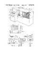
- FIG. 1is a top view of the circuit board having mounted thereon a number of EPROMs that are to be programmed in accordance with the principles of the invention
- FIG. 2is a perspective view of a hardware configuration that may be used to simultaneously program a number of EPROMs respectively located on a number of circuit boards;
- FIG. 3is a schematic block diagram showing the data path interrelationship between the hardware units shown in FIG. 2, and
- FIG. 4is a flow chart of a series of programmed method steps to be followed for simultaneously programming a number of EPROMs with the hardware shown in the other FIGURES.
- a printed circuit board or pack 10having a plurality of EPROMs (Erasable Programmable Read Only Memories) 11 mounted thereon along with a number of other integrated circuits (ICs) and electrical components.
- EPROMsErasable Programmable Read Only Memories
- a typical EPROMmay consist of 2,048 addressable memory sites in which data bytes of 8 bits may be stored.
- EPROMsare constructed with quartz windows 12 through which ultraviolet light may be transmitted to erase and initially set all the memory byte sites in "all-ones" conditions.
- the EPROMare further characterized in that they may only be reset by electrical bit pulses that function to shift a bit from the one state to a zero state.
- the circuit board 10includes printed circuit paths that run from the EPROMs and the other components to a series of pads or contact fingers 13 located along the right-hand end of the board.
- the end of the board with the contact fingersis adapted to be inserted into a socket-like connector 14 (see FIG. 2) mounted in a housing 15.
- the housingis constructed with a number of connectors 14 to receive not only EPROM boards but also other boards such as power supply boards 16, a CPU interface board 17 and a master program board 18, similar to board 10.
- the interface boardis designed to route successive bytes of data signals received over a cable 19 to the respective EPROMs 11 mounted on a number of boards 10.
- Each byte site in each EPROMcomprises a number, e.g., 8, of bit locations corresponding to the number of bits in each byte.
- the bit locationsupon receipt of a program data word signal, may be held in a one state or switched to a zero state.
- the interface board 17is controlled by a central processing unit (CPU) 21 which may be a minicomputer such as a PDP 8, manufactured by the Digital Equipment Company.
- CPUcentral processing unit
- This particular minicomputeris a 12 bit machine which means that it communicates through a data channel that consists of 12 simultaneous inputs or outputs, each bit being a one or a zero.
- the 12 outputsare simultaneously transmitted over the cable 19 and routed by the interface board 17 to identical EPROMs located on a series of 12 EPROM packs loaded into the cabinet.
- the interface boardunder the control of the CPU, is also effective upon command to successively read each programmed site and route the stored data back into the central processing unit 21 for anlaysis and verification.
- the master program pack 18is identical in construction to the circuit boards 10, but this pack is previously programmed or set in accordance with the data to be imparted to the EPROMs 11 on the other circuit boards 10.
- the interface 17, upon command from the CPU 21,reads the data setting of the memory sites on the master programmed board 18 and impresses the stored data on the program source 22, which may be in the form of a disc memory.
- the systemalso includes a data terminal 23 with a keyboard 24 and a visual display 25 that is operative to introduce control signals into the CPU to initially set the overall control program in the CPU.
- the terminalis also utilized to provide visual indication of various conditions in the system such as indication that the EPROM boards are properly seated in the connectors 14 or that one of the connectors does not have a board 10 installed therein.
- Terminal 23is also capable of providing a display of the data setting of each memory site.
- circuit packs 10are initially erased by exposure to ultraviolet light, which functions to set all the bit memory locations in the one (1) state. Twelve circuit packs are inserted in the connectors 14. In the normal programming operation each data byte is routed over 12 wires in the cable 19 through the interface, bit by bit, to corresponding memory locations in 12 EPROMs mounted on the individual circuit packs. Zero data bits are effective to reset the memory locations to the zero state while one (1) data bits do not disturb the original memory setting.
- the programmed data bytesare successively routed as control signals to set each data site in each corresponding EPROM on each of the circuit packs. Normally, about 50 milliseconds is consumed to simultaneously program or set the byte sites on the 12 corresponding memories. Even if only one circuit pack 10 is being programmed, it will take about 50 milliseconds to program and set each memory site.
- the stream of data signals used to program the memoryincludes a number of data bytes of "all-ones" (1's) which may be indicative of intelligent (real) data, a space, or a site to be reserved for future programming.
- the present inventionprovides methods and facilities for aborting the programming of a memory site which is already set in accordance with data specified to be inserted to that site.
- the methodcontemplates verifying the data setting of each site even though the data byte specified for that location was not applied to the site because it consisted of all one bits.
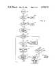
- FIG. 4is a flow chart indicating the manner in which the minicomputer associated with the apparatus shown in the other view is programmed and functions to control the selective programming of memory sites in a number of groups of EPROMs mounted on individual circuit boards.
- the systemis controlled by the minicomputer 21 which is programmed to function in accordance with the flow chart.
- the interface 17provides the data link between the CPU 21 and the individual circuit packs 10. This interface ensures that each data bit is routed simultaneously to memory locations in EPROMs mounted on the twelve packs 10.
- a determination 42is made as to the presence of the circuit packs 10. If a pack 10 is missing or not properly connected, a visual indication is provided on the display of terminal 23. If all the packs 10 are missing, the programming is stopped 43. However, if one or more packs are present, the programming cycle may proceed. Next, each EPROM on each circuit pack is checked 44 to ensure that all the memory sites have been erased and are set in the "all-one" (1) state. If all the memories have not been erased and set in the one (1) state, the programming cycle is interruped 45 and this information is presented on the terminal display 25. Actual program setting of the EPROMs may now commence 46 and the cyclic programming loop is initiated into operation. The CPU 21 successfully calls 47 each data byte from the disc memory 22 and each bit is impressed over the twelve lines of cable 19 to the CPU interface 17 to be routed to identical address sites on twelve corresponding EPROMs mounted on the twelve circuit packs 10.
- Each byte called from storageis analyzed 48 and if the byte does not consist of all ones (1s), the byte is programmed 49 into appropriate memory sites in each EPROM on each of the twelve circuit packs 10.
- the data bytes set into the twelve memory sites on the twelve EPROMsare read 51 and verified 52 against the programmed data 48-49 that was intended to the imparted to the EPROM memory sites. If the data programmed into an EPROM is not exactly in accordance with the data received from the CPU 21, the programming is interrupted and an error indication 53 is reported and displayed at the terminal 23. After reporting all errors 53, and the CPU 21 determines that all packs 10 have errors 54, programming is stopped 56.
- the programming of those packsis stopped 57 and the programming of the other packs continues.
- the next byte to be programmedis called from the source 22.
- the EPROM program operation 49is bypassed 58 and an intermediate verification 51 of the memory sites of each pack 10 is made. Inasmuch as the program operation 49 is bypassed in the "all-ones" instance, the overall time required to program the groups of EPROMs on each board is reduced. The site that is not programmed is verified and upon verification that the data of that EPROM site is at an "all-ones" (1s) condition, the program cycle continues and the next byte to be programmed is immediately called from the program source 22.
- the program source 22which may be in the form of a disc memory, has data stored on it in accordance with a program readout of the master program pack 18.
- the minicomputer 21may be connected to a modem 61 which in turn is linked through a telephone network 62 to a modem 63 associated with a host computer 64.
- the host computer 64will provide the master data to be stored on the system disc memory 22.
Landscapes
- Read Only Memory (AREA)
Abstract
Description
Claims (1)
Priority Applications (1)
| Application Number | Priority Date | Filing Date | Title |
|---|---|---|---|
| US06/392,053US4578751A (en) | 1982-06-25 | 1982-06-25 | System for simultaneously programming a number of EPROMs |
Applications Claiming Priority (1)
| Application Number | Priority Date | Filing Date | Title |
|---|---|---|---|
| US06/392,053US4578751A (en) | 1982-06-25 | 1982-06-25 | System for simultaneously programming a number of EPROMs |
Publications (1)
| Publication Number | Publication Date |
|---|---|
| US4578751Atrue US4578751A (en) | 1986-03-25 |
Family
ID=23549058
Family Applications (1)
| Application Number | Title | Priority Date | Filing Date |
|---|---|---|---|
| US06/392,053Expired - LifetimeUS4578751A (en) | 1982-06-25 | 1982-06-25 | System for simultaneously programming a number of EPROMs |
Country Status (1)
| Country | Link |
|---|---|
| US (1) | US4578751A (en) |
Cited By (22)
| Publication number | Priority date | Publication date | Assignee | Title |
|---|---|---|---|---|
| US4763305A (en)* | 1985-11-27 | 1988-08-09 | Motorola, Inc. | Intelligent write in an EEPROM with data and erase check |
| US4791661A (en)* | 1986-07-01 | 1988-12-13 | Global Technology International, Inc. | Portable EPROM programming and data transfer apparatus |
| US4799021A (en)* | 1986-07-22 | 1989-01-17 | Sgs Microelettronica S.P.A. | Method and apparatus for testing EPROM type semiconductor devices during burn-in |
| US4811294A (en)* | 1985-06-21 | 1989-03-07 | Mitsubishi Denki Kabushiki Kaisha | Data integrity verifying circuit for electrically erasable and programmable read only memory (EEPROM) |
| US5003507A (en)* | 1988-09-06 | 1991-03-26 | Simon Johnson | EPROM emulator for selectively simulating a variety of different paging EPROMs in a test circuit |
| US5036488A (en)* | 1989-03-24 | 1991-07-30 | David Motarjemi | Automatic programming and erasing device for electrically erasable programmable read-only memories |
| US5043884A (en)* | 1988-07-14 | 1991-08-27 | Siemens Aktiengesellschaft | Communications installation with communications terminal equipment provided with prescribed functions defined and controlled by a communications installation with information transmission |
| US5127097A (en)* | 1987-11-09 | 1992-06-30 | Mitsubishi Denki Kabushiki Kaisha | Memory writing apparatus |
| US5164573A (en)* | 1988-06-28 | 1992-11-17 | Alps Electric Co., Ltd. | Optical reading device |
| US5495450A (en)* | 1994-06-20 | 1996-02-27 | Motorola, Inc. | Method and assembly for mounting an electronic device having an optically erasable surface |
| US5581510A (en)* | 1994-06-28 | 1996-12-03 | Mitsubishi Denki Kabushiki Kaisha | Method of testing flash memory |
| US6009496A (en)* | 1997-10-30 | 1999-12-28 | Winbond Electronics Corp. | Microcontroller with programmable embedded flash memory |
| US6229737B1 (en) | 1996-12-12 | 2001-05-08 | Ericsson Inc. | Method and apparatus for initializing semiconductor memory |
| EP1100091A1 (en)* | 1999-11-10 | 2001-05-16 | Data I/O Corporation | High speed programmer system |
| US6542956B1 (en)* | 1996-11-05 | 2003-04-01 | Sandisk Corporation | Latched address multi-chunk write to EEPROM |
| US6584553B2 (en)* | 2000-07-31 | 2003-06-24 | Exatron, Inc. | Method and system for sequentially programming memory-containing integrated circuits |
| US20040153590A1 (en)* | 2001-06-12 | 2004-08-05 | Andre Roger | Method for programming/parallel programming of onboard flash memory by multiple acces bus |
| US20040186948A1 (en)* | 1991-07-26 | 2004-09-23 | Lofgren Karl M. J. | Device and method for controlling solid-state memory system |
| US20040237000A1 (en)* | 2003-05-08 | 2004-11-25 | Micron Technology, Inc. | Program failure recovery |
| EP2003566A1 (en) | 2007-06-08 | 2008-12-17 | Robert Bosch Gmbh | Method and control device for operating a non-volatile memory, in particular for use in motor vehicles |
| US20080316681A1 (en)* | 2005-12-28 | 2008-12-25 | Showa Denko K.K. | Capacitor and Method for Manufacturing Same |
| US20090312857A1 (en)* | 2008-06-16 | 2009-12-17 | Data I/O Corporation | Programmer actuator system and method of operation thereof |
Citations (12)
| Publication number | Priority date | Publication date | Assignee | Title |
|---|---|---|---|---|
| US3969618A (en)* | 1974-11-29 | 1976-07-13 | Xerox Corporation | On line PROM handling system |
| US4093998A (en)* | 1976-09-29 | 1978-06-06 | Gulf & Western Industries, Inc. | Programming module for programmable controller using a microprocessor |
| US4106105A (en)* | 1977-02-28 | 1978-08-08 | The Singer Company | Zero detector |
| US4238839A (en)* | 1979-04-19 | 1980-12-09 | National Semiconductor Corporation | Laser programmable read only memory |
| US4244032A (en)* | 1977-12-16 | 1981-01-06 | Oliver Douglas E | Apparatus for programming a PROM by propagating data words from an address bus to the PROM data terminals |
| US4377857A (en)* | 1980-11-18 | 1983-03-22 | Fairchild Camera & Instrument | Electrically erasable programmable read-only memory |
| US4382279A (en)* | 1978-04-25 | 1983-05-03 | Compagnie Internationale Pour L'informatique Cii-Honeywell Bull (Societe Anonyme) | Single chip microprocessor with on-chip modifiable memory |
| US4441164A (en)* | 1980-07-03 | 1984-04-03 | Ing. C. Olivetti & C., S.P.A. | Electronic teleprinting apparatus including a removable programmed EPROM |
| US4443185A (en)* | 1979-03-13 | 1984-04-17 | Smith Thomas M | Heating of webs |
| US4460982A (en)* | 1982-05-20 | 1984-07-17 | Intel Corporation | Intelligent electrically programmable and electrically erasable ROM |
| US4498151A (en)* | 1980-04-17 | 1985-02-05 | Texas Instruments Incorporated | On board non-volatile memory programming |
| US4545038A (en)* | 1982-04-05 | 1985-10-01 | Texas Instruments Incorporated | Precharged discharge sensing for EPROM |
- 1982
- 1982-06-25USUS06/392,053patent/US4578751A/ennot_activeExpired - Lifetime
Patent Citations (12)
| Publication number | Priority date | Publication date | Assignee | Title |
|---|---|---|---|---|
| US3969618A (en)* | 1974-11-29 | 1976-07-13 | Xerox Corporation | On line PROM handling system |
| US4093998A (en)* | 1976-09-29 | 1978-06-06 | Gulf & Western Industries, Inc. | Programming module for programmable controller using a microprocessor |
| US4106105A (en)* | 1977-02-28 | 1978-08-08 | The Singer Company | Zero detector |
| US4244032A (en)* | 1977-12-16 | 1981-01-06 | Oliver Douglas E | Apparatus for programming a PROM by propagating data words from an address bus to the PROM data terminals |
| US4382279A (en)* | 1978-04-25 | 1983-05-03 | Compagnie Internationale Pour L'informatique Cii-Honeywell Bull (Societe Anonyme) | Single chip microprocessor with on-chip modifiable memory |
| US4443185A (en)* | 1979-03-13 | 1984-04-17 | Smith Thomas M | Heating of webs |
| US4238839A (en)* | 1979-04-19 | 1980-12-09 | National Semiconductor Corporation | Laser programmable read only memory |
| US4498151A (en)* | 1980-04-17 | 1985-02-05 | Texas Instruments Incorporated | On board non-volatile memory programming |
| US4441164A (en)* | 1980-07-03 | 1984-04-03 | Ing. C. Olivetti & C., S.P.A. | Electronic teleprinting apparatus including a removable programmed EPROM |
| US4377857A (en)* | 1980-11-18 | 1983-03-22 | Fairchild Camera & Instrument | Electrically erasable programmable read-only memory |
| US4545038A (en)* | 1982-04-05 | 1985-10-01 | Texas Instruments Incorporated | Precharged discharge sensing for EPROM |
| US4460982A (en)* | 1982-05-20 | 1984-07-17 | Intel Corporation | Intelligent electrically programmable and electrically erasable ROM |
Non-Patent Citations (10)
| Title |
|---|
| J. Javetski, PROM Programmers Move From the Lab to the Assembly Line, Microsystem Development (Jul. 1982), pp. 41 45.* |
| J. Javetski, PROM Programmers Move From the Lab to the Assembly Line, Microsystem Development (Jul. 1982), pp. 41-45. |
| J. MacDougall, Powered Down Bipolar PROMs, Interface Age (Apr. 1980) pp. 108 112.* |
| J. MacDougall, Powered Down Bipolar PROMs, Interface Age (Apr. 1980) pp. 108-112. |
| R. Coates, Nanocomp E.P.R.O.M. Programmer, Wireless World (Jan. 1982, vol. 88, No. 1552) pp. 30 33.* |
| R. Coates, Nanocomp E.P.R.O.M. Programmer, Wireless World (Jan. 1982, vol. 88, No. 1552) pp. 30-33. |
| R. Glaser, Program Those 2708 s, Byte (Apr. 1980, vol. 5, No. 4) pp. 198 210.* |
| R. Glaser, Program Those 2708s, Byte (Apr. 1980, vol. 5, No. 4) pp. 198-210. |
| T. Hayek, Simple and Low Cost PROM Programmer, Kilobaud (Jul. 1978) pp. 94 94.* |
| T. Hayek, Simple and Low-Cost PROM Programmer, Kilobaud (Jul. 1978) pp. 94-94. |
Cited By (37)
| Publication number | Priority date | Publication date | Assignee | Title |
|---|---|---|---|---|
| US4811294A (en)* | 1985-06-21 | 1989-03-07 | Mitsubishi Denki Kabushiki Kaisha | Data integrity verifying circuit for electrically erasable and programmable read only memory (EEPROM) |
| US4763305A (en)* | 1985-11-27 | 1988-08-09 | Motorola, Inc. | Intelligent write in an EEPROM with data and erase check |
| US4791661A (en)* | 1986-07-01 | 1988-12-13 | Global Technology International, Inc. | Portable EPROM programming and data transfer apparatus |
| US4799021A (en)* | 1986-07-22 | 1989-01-17 | Sgs Microelettronica S.P.A. | Method and apparatus for testing EPROM type semiconductor devices during burn-in |
| US5127097A (en)* | 1987-11-09 | 1992-06-30 | Mitsubishi Denki Kabushiki Kaisha | Memory writing apparatus |
| US5164573A (en)* | 1988-06-28 | 1992-11-17 | Alps Electric Co., Ltd. | Optical reading device |
| US5043884A (en)* | 1988-07-14 | 1991-08-27 | Siemens Aktiengesellschaft | Communications installation with communications terminal equipment provided with prescribed functions defined and controlled by a communications installation with information transmission |
| US5003507A (en)* | 1988-09-06 | 1991-03-26 | Simon Johnson | EPROM emulator for selectively simulating a variety of different paging EPROMs in a test circuit |
| US5036488A (en)* | 1989-03-24 | 1991-07-30 | David Motarjemi | Automatic programming and erasing device for electrically erasable programmable read-only memories |
| US20040186948A1 (en)* | 1991-07-26 | 2004-09-23 | Lofgren Karl M. J. | Device and method for controlling solid-state memory system |
| US8125834B2 (en) | 1991-07-26 | 2012-02-28 | Sandisk Technologies Inc. | Device and method for controlling solid-state memory system |
| US7688643B2 (en) | 1991-07-26 | 2010-03-30 | Sandisk Corporation | Device and method for controlling solid-state memory system |
| US20100064098A1 (en)* | 1991-07-26 | 2010-03-11 | Lofgren Karl M J | Device and Method for Controlling Solid-State Memory System |
| US5495450A (en)* | 1994-06-20 | 1996-02-27 | Motorola, Inc. | Method and assembly for mounting an electronic device having an optically erasable surface |
| US5581510A (en)* | 1994-06-28 | 1996-12-03 | Mitsubishi Denki Kabushiki Kaisha | Method of testing flash memory |
| US20090228644A1 (en)* | 1996-11-05 | 2009-09-10 | Lee Douglas J | Latched Address Multi-Chunk Write to EEPROM |
| US20030200380A1 (en)* | 1996-11-05 | 2003-10-23 | Lee Douglas J. | Latched address multi-chunk write to EEPROM |
| US6542956B1 (en)* | 1996-11-05 | 2003-04-01 | Sandisk Corporation | Latched address multi-chunk write to EEPROM |
| US6829673B2 (en) | 1996-11-05 | 2004-12-07 | Sandisk Corporation | Latched address multi-chunk write to EEPROM |
| US7890694B2 (en) | 1996-11-05 | 2011-02-15 | Sandisk Corporation | Latched address multi-chunk write to EEPROM |
| US6229737B1 (en) | 1996-12-12 | 2001-05-08 | Ericsson Inc. | Method and apparatus for initializing semiconductor memory |
| US6009496A (en)* | 1997-10-30 | 1999-12-28 | Winbond Electronics Corp. | Microcontroller with programmable embedded flash memory |
| EP1100091A1 (en)* | 1999-11-10 | 2001-05-16 | Data I/O Corporation | High speed programmer system |
| US6584553B2 (en)* | 2000-07-31 | 2003-06-24 | Exatron, Inc. | Method and system for sequentially programming memory-containing integrated circuits |
| US20040153590A1 (en)* | 2001-06-12 | 2004-08-05 | Andre Roger | Method for programming/parallel programming of onboard flash memory by multiple acces bus |
| US7102383B2 (en)* | 2001-06-12 | 2006-09-05 | Stmicroelectronics Sa | Method for programming/parallel programming of onboard flash memory by multiple access bus |
| US20040237000A1 (en)* | 2003-05-08 | 2004-11-25 | Micron Technology, Inc. | Program failure recovery |
| US7783934B2 (en)* | 2003-05-08 | 2010-08-24 | Micron Technology, Inc. | Program failure recovery |
| US20100325479A1 (en)* | 2003-05-08 | 2010-12-23 | Micron Technology, Inc. | Program failure recovery |
| US20080263412A1 (en)* | 2003-05-08 | 2008-10-23 | Micron Technology, Inc. | Program failure recovery |
| US8074122B2 (en) | 2003-05-08 | 2011-12-06 | Micron Technology, Inc. | Program failure recovery |
| US7392436B2 (en)* | 2003-05-08 | 2008-06-24 | Micron Technology, Inc. | Program failure recovery |
| US20080316681A1 (en)* | 2005-12-28 | 2008-12-25 | Showa Denko K.K. | Capacitor and Method for Manufacturing Same |
| EP2003566A1 (en) | 2007-06-08 | 2008-12-17 | Robert Bosch Gmbh | Method and control device for operating a non-volatile memory, in particular for use in motor vehicles |
| US8019931B2 (en) | 2007-06-08 | 2011-09-13 | Robert Bosch Gmbh | Method and control unit for operating a non-volatile memory, in particular for use in motor vehicles |
| US20090312857A1 (en)* | 2008-06-16 | 2009-12-17 | Data I/O Corporation | Programmer actuator system and method of operation thereof |
| US8245388B2 (en)* | 2008-06-16 | 2012-08-21 | Data I/O Corporation | Programmer actuator system and method of operation thereof |
Similar Documents
| Publication | Publication Date | Title |
|---|---|---|
| US4578751A (en) | System for simultaneously programming a number of EPROMs | |
| US4471457A (en) | Supervisory control of peripheral subsystems | |
| US5901279A (en) | Connection of spares between multiple programmable devices | |
| US4414669A (en) | Self-testing pipeline processors | |
| DE3901579C2 (en) | ||
| US4196386A (en) | Method and portable apparatus for testing digital printed circuit boards | |
| EP0784818B1 (en) | Microprocessor programming using a state machine | |
| EP0180128A2 (en) | User interface processor for computer network | |
| EP0169244B1 (en) | Method of and apparatus for diagnosing channel control unit | |
| US4076970A (en) | Switching system having a central controller for accessing individual telephone circuits for testing | |
| US5058112A (en) | Programmable fault insertion circuit | |
| GB2201016A (en) | Memories and the testing thereof | |
| US4620273A (en) | Terminal control system and method of terminal control | |
| CN101079328A (en) | Parallel programming of flash memory during in-circuit test | |
| US4174805A (en) | Method and apparatus for transmitting data to a predefined destination bus | |
| GB1579165A (en) | Data processing apparatus | |
| EP0086137B1 (en) | A programmable machine card addressing device for the security of exchanges on the bus | |
| US6708295B2 (en) | Circuit and method, for storing data prior to and after determining failure | |
| US6598176B1 (en) | Apparatus for estimating microcontroller and method thereof | |
| US4574167A (en) | Method and apparatus for configurable line testing | |
| EP1104579B1 (en) | Memory supervision | |
| US5965957A (en) | Switching apparatus, in particular for systems under test | |
| EP0039665A1 (en) | A method and apparatus for tracing a sequence comprising a series of transfers of binary message words | |
| US3805243A (en) | Apparatus and method for determining partial memory chip categories | |
| US4305136A (en) | Method of symptom compression |
Legal Events
| Date | Code | Title | Description |
|---|---|---|---|
| AS | Assignment | Owner name:WESTERN ELECTRIC COMPANY, INCORPORATED, 222 BROADW Free format text:ASSIGNMENT OF ASSIGNORS INTEREST.;ASSIGNOR:ERWIN, EDWARD A.;REEL/FRAME:004017/0269 Effective date:19820616 | |
| AS | Assignment | Owner name:AT & T TECHNOLOGIES, INC., Free format text:CHANGE OF NAME;ASSIGNOR:WESTERN ELECTRIC COMPANY, INCORPORATED;REEL/FRAME:004251/0868 Effective date:19831229 | |
| STCF | Information on status: patent grant | Free format text:PATENTED CASE | |
| CC | Certificate of correction | ||
| FEPP | Fee payment procedure | Free format text:PAYOR NUMBER ASSIGNED (ORIGINAL EVENT CODE: ASPN); ENTITY STATUS OF PATENT OWNER: LARGE ENTITY | |
| FPAY | Fee payment | Year of fee payment:4 | |
| FPAY | Fee payment | Year of fee payment:8 | |
| FEPP | Fee payment procedure | Free format text:PAYOR NUMBER ASSIGNED (ORIGINAL EVENT CODE: ASPN); ENTITY STATUS OF PATENT OWNER: LARGE ENTITY Free format text:PAYER NUMBER DE-ASSIGNED (ORIGINAL EVENT CODE: RMPN); ENTITY STATUS OF PATENT OWNER: LARGE ENTITY | |
| FPAY | Fee payment | Year of fee payment:12 |