US4577932A - Multi-spot modulator using a laser diode - Google Patents
Multi-spot modulator using a laser diodeDownload PDFInfo
- Publication number
- US4577932A US4577932AUS06/608,222US60822284AUS4577932AUS 4577932 AUS4577932 AUS 4577932AUS 60822284 AUS60822284 AUS 60822284AUS 4577932 AUS4577932 AUS 4577932A
- Authority
- US
- United States
- Prior art keywords
- modulator
- laser
- light
- laser diode
- spot
- Prior art date
- Legal status (The legal status is an assumption and is not a legal conclusion. Google has not performed a legal analysis and makes no representation as to the accuracy of the status listed.)
- Expired - Fee Related
Links
Images

Classifications
- G—PHYSICS
- G02—OPTICS
- G02F—OPTICAL DEVICES OR ARRANGEMENTS FOR THE CONTROL OF LIGHT BY MODIFICATION OF THE OPTICAL PROPERTIES OF THE MEDIA OF THE ELEMENTS INVOLVED THEREIN; NON-LINEAR OPTICS; FREQUENCY-CHANGING OF LIGHT; OPTICAL LOGIC ELEMENTS; OPTICAL ANALOGUE/DIGITAL CONVERTERS
- G02F1/00—Devices or arrangements for the control of the intensity, colour, phase, polarisation or direction of light arriving from an independent light source, e.g. switching, gating or modulating; Non-linear optics
- G02F1/01—Devices or arrangements for the control of the intensity, colour, phase, polarisation or direction of light arriving from an independent light source, e.g. switching, gating or modulating; Non-linear optics for the control of the intensity, phase, polarisation or colour
- G02F1/11—Devices or arrangements for the control of the intensity, colour, phase, polarisation or direction of light arriving from an independent light source, e.g. switching, gating or modulating; Non-linear optics for the control of the intensity, phase, polarisation or colour based on acousto-optical elements, e.g. using variable diffraction by sound or like mechanical waves
- G—PHYSICS
- G06—COMPUTING OR CALCULATING; COUNTING
- G06K—GRAPHICAL DATA READING; PRESENTATION OF DATA; RECORD CARRIERS; HANDLING RECORD CARRIERS
- G06K15/00—Arrangements for producing a permanent visual presentation of the output data, e.g. computer output printers
- G06K15/02—Arrangements for producing a permanent visual presentation of the output data, e.g. computer output printers using printers
- G06K15/12—Arrangements for producing a permanent visual presentation of the output data, e.g. computer output printers using printers by photographic printing, e.g. by laser printers
- G06K15/1238—Arrangements for producing a permanent visual presentation of the output data, e.g. computer output printers using printers by photographic printing, e.g. by laser printers simultaneously exposing more than one point
Definitions
- Multi-spot modulatorsare used for high speed recording of data on a light sensitive material in laser printers, plotters and optical data storage devices.
- a multi-spot modulatoris faster than single spot modulators since it records a plurality of bits simultaneously.
- This inventionrelates to the use of an acousto-optic modulator as a multi-spot modulator.
- the prior artgenerates multiple spots with acousto-optic modulators by using multiple frequencies simultaneously (such as the multi-spot modulators sold by the Isomet Corporation, U.S.A.), by using multiple transducers simultaneously or by imaging a multi-spot acoustic pattern using the Scophony effect to avoid the image degradation caused by the motion of the acoustic wave.
- the current inventionuses a single frequency amplitude modulation (AM) to modulate the acousto-optic modulator and uses a short light pulse from a laser diode to avoid the effects of the acoustic wave motion.
- AMsingle frequency amplitude modulation
- the low duty cycle and high peak power of the laser diode in this inventionalso allows the incorporation of frequency doubling using a crystal with non-linear optical properties.
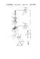
- FIG. 1represents an embodiment of the invention
- FIG. 2represents an embodiment of the invention when used with a frequency doubling crystal.
- the preferred embodimentconsists of a laser diode 1, a focussing lens 2 placed to project the magnified image of the laser diode emitting apperture onto an acousto-optic modulator 3.
- the undiffracted beam 4 from the acousto-optic modulatoris not used while the diffracted beam 5 is focussed by a second lens 6 to form an image of the acoustic field inside the modulator 3 onto a light sensitive material 7.
- the distances between the componentsare such that the image of laser diode 1 is formed inside modulator 3 and the image of the acoustic wave inside modulator 3 is formed on the light sensitive material 7.
- the focal length and size of the first lens 2is chosen to capture the radiated light from the laser diode and illuminate the desired portion of the acousto-optic modulator 3.
- the focal length of the second lensis chosen to reduce the image of the acoustic wave by the desired amount.
- diode 1will be a pulsed laser diode of about 10 W peak power, such as available from RCA or Sanders Associateds (USA).
- Lens 2will magnify the 20 ⁇ 200 ⁇ m exit aperture of this laser diode by about a factor of 10, the forming an image of about 200 ⁇ 2000 ⁇ m in the acousto-optic modulator.
- the modulatoris of standard construction, such as available from Isomet (USA) or Crystal Technology (USA) operating at 200 MHz.
- the laser diode driver and modulator driverare items well known to those versed in the art.
- the laser diode 1is of the pulsed type.
- the laser-diode driver 8generates a narrow current pulse of about 1 nS duration.
- the AM modulator 9converts the input data 10 to an amplitude modulated carrier at the operating frequency of the acousto-optic cell, in this case 200 MHz.
- the data rateis selected such that a single bit is longer than the exposure pulse from the laser diode. In this embodiment one data bit is about 10 nS. Since the acoustic wave travels in the acousto-optics modulator at a velocity of about 3.63 mm/ ⁇ S' (for Lead Molibdate), it will cover the 2 mm aperture in about 550 nS. Assuming 10 nS per bit this will allow 55 bits to be inside the acousto-optic modulator aperture at any time, thus the sync pulse 11 should be supplied every 55 bits of data.
- the desired data pattern 10is fed to the acousto-optic modulator 3 via the AM modulator 9.
- the bit patternmodulates a carrier which generates an acoustic wave inside 3 by using a piezo-electric transducer bonded to the acousto-optic material.
- the sync pulse 11When all the data bits were converted to acoustic energy the sync pulse 11 generates a narrow light pulse out of laser diode 1. This light pulse images the acoustic field onto light sensitive material 7 and forms a permanent record of the data pattern 10.
- By moving material 7a new bit pattern can be recorded with a new light pulse. Since the light pulse is much shorter than a single data bit the image on material 7 is not degraded by the fact that the acoustic wave is moving while being imaged.
- the image of the acoustic waveis formed by the well known mechanism of diffracting the light.
- the travelling acoustic waveacts as a diffraction grating causing light to be diffracted each time it encounters a packet of acoustic energy being generated by the input data.
- the operation of the acousto-optic modulatoris similar to its well known application as a laser light modulator. As in all applications of this modulator it should be oriented in a way that the light will enter it at the Bragg angle to maximize the diffraction efficiency and therefore the output light.
- FIG. 2A variation on the preferred embodiment is shown in FIG. 2.
- the wavelength of the laser diodeis halved by using a non-linear optical crystal 12. These crystals are available from Cleveland Crystals (USA) and are made of non-linear optical materials such as LiIO 3 .
- the lightis focussed through the crystal 12 by a lens 13 in order to increase the power density.
- the angle of the crystalis adjusted to maximize the second harmonic generation.
- the output light, at the second harmonicis focussed into the acousto-optic modulator.
- the Bragg angleis, of course, re-adjusted for the new wavelength.
- Using the second harmonichas the advantage of higher resolution and, since currently available laser diodes operate in the infrared, makes the operation visible.
Landscapes
- Physics & Mathematics (AREA)
- Optics & Photonics (AREA)
- Engineering & Computer Science (AREA)
- General Physics & Mathematics (AREA)
- Nonlinear Science (AREA)
- General Engineering & Computer Science (AREA)
- Theoretical Computer Science (AREA)
- Laser Beam Printer (AREA)
Abstract
Description
Multi-spot modulators are used for high speed recording of data on a light sensitive material in laser printers, plotters and optical data storage devices. A multi-spot modulator is faster than single spot modulators since it records a plurality of bits simultaneously. This invention relates to the use of an acousto-optic modulator as a multi-spot modulator. The prior art generates multiple spots with acousto-optic modulators by using multiple frequencies simultaneously (such as the multi-spot modulators sold by the Isomet Corporation, U.S.A.), by using multiple transducers simultaneously or by imaging a multi-spot acoustic pattern using the Scophony effect to avoid the image degradation caused by the motion of the acoustic wave. It is the object of this invention to make a multi-spot modulator in order to generate a permanent optical record of a data pattern using a laser diode. The current invention uses a single frequency amplitude modulation (AM) to modulate the acousto-optic modulator and uses a short light pulse from a laser diode to avoid the effects of the acoustic wave motion. The low duty cycle and high peak power of the laser diode in this invention also allows the incorporation of frequency doubling using a crystal with non-linear optical properties.
Further details of the invention will become apparent by considering the preferred embodiment in conjunction with the following drawings, in which
FIG. 1 represents an embodiment of the invention and
FIG. 2 represents an embodiment of the invention when used with a frequency doubling crystal.
Referring now to FIG. 1, the preferred embodiment consists of a laser diode 1, a focussinglens 2 placed to project the magnified image of the laser diode emitting apperture onto an acousto-optic modulator 3. The undiffracted beam 4 from the acousto-optic modulator is not used while thediffracted beam 5 is focussed by a second lens 6 to form an image of the acoustic field inside themodulator 3 onto a light sensitive material 7. The distances between the components are such that the image of laser diode 1 is formed insidemodulator 3 and the image of the acoustic wave insidemodulator 3 is formed on the light sensitive material 7. The focal length and size of thefirst lens 2 is chosen to capture the radiated light from the laser diode and illuminate the desired portion of the acousto-optic modulator 3. The focal length of the second lens is chosen to reduce the image of the acoustic wave by the desired amount. In the preferred embodiment diode 1 will be a pulsed laser diode of about 10 W peak power, such as available from RCA or Sanders Associateds (USA).Lens 2 will magnify the 20×200 μm exit aperture of this laser diode by about a factor of 10, the forming an image of about 200×2000 μm in the acousto-optic modulator. The modulator is of standard construction, such as available from Isomet (USA) or Crystal Technology (USA) operating at 200 MHz. The laser diode driver and modulator driver are items well known to those versed in the art.
The laser diode 1 is of the pulsed type. The laser-diode driver 8 generates a narrow current pulse of about 1 nS duration. The AM modulator 9 converts theinput data 10 to an amplitude modulated carrier at the operating frequency of the acousto-optic cell, in this case 200 MHz. The data rate is selected such that a single bit is longer than the exposure pulse from the laser diode. In this embodiment one data bit is about 10 nS. Since the acoustic wave travels in the acousto-optics modulator at a velocity of about 3.63 mm/μS' (for Lead Molibdate), it will cover the 2 mm aperture in about 550 nS. Assuming 10 nS per bit this will allow 55 bits to be inside the acousto-optic modulator aperture at any time, thus the sync pulse 11 should be supplied every 55 bits of data.
In operation the desireddata pattern 10 is fed to the acousto-optic modulator 3 via the AM modulator 9. The bit pattern modulates a carrier which generates an acoustic wave inside 3 by using a piezo-electric transducer bonded to the acousto-optic material. When all the data bits were converted to acoustic energy the sync pulse 11 generates a narrow light pulse out of laser diode 1. This light pulse images the acoustic field onto light sensitive material 7 and forms a permanent record of thedata pattern 10. By moving material 7 a new bit pattern can be recorded with a new light pulse. Since the light pulse is much shorter than a single data bit the image on material 7 is not degraded by the fact that the acoustic wave is moving while being imaged.
The image of the acoustic wave is formed by the well known mechanism of diffracting the light. The travelling acoustic wave acts as a diffraction grating causing light to be diffracted each time it encounters a packet of acoustic energy being generated by the input data. The operation of the acousto-optic modulator is similar to its well known application as a laser light modulator. As in all applications of this modulator it should be oriented in a way that the light will enter it at the Bragg angle to maximize the diffraction efficiency and therefore the output light.
A variation on the preferred embodiment is shown in FIG. 2. In this embodiment the wavelength of the laser diode is halved by using a non-linear optical crystal 12. These crystals are available from Cleveland Crystals (USA) and are made of non-linear optical materials such as LiIO3. The light is focussed through the crystal 12 by alens 13 in order to increase the power density. The angle of the crystal is adjusted to maximize the second harmonic generation. The output light, at the second harmonic, is focussed into the acousto-optic modulator. The Bragg angle is, of course, re-adjusted for the new wavelength. Using the second harmonic has the advantage of higher resolution and, since currently available laser diodes operate in the infrared, makes the operation visible.
Since the efficiency of frequency doubling increases with the square of the power density using a pulsed laser diode with a low duty cycle and high peak power is desireable.
Claims (3)
1. A multi-spot light modulator comprising:
a laser operating in the pulsed mode; an acousto-optic modulator and means for converting a data pattern into a corresponding acoustic wave inside said modulator, said modulator for diffracting a beam from said laser; a lens for focussing a light pulse from said laser onto said acoustic wave;
a light sensitive material for generating a permanent record;
a second lens located in said diffracted output beam of said modulator for forming an image of said acoustic wave onto said light sensitive material; and means for synchronizing said light pulse with said data pattern in order to generate a permanent record of said data pattern on said light sensitive material.
2. A multi-spot light modulator as described in claim 1 further comprising a crystal of non-linear optical material positioned in the path of the laser pulse in order to double the frequency of the laser light; and, a focussing lens for concentrating light output of said laser into said non linear material in order to increase the efficiency of the frequency doubling.
3. A multi-spot modulator as described in claims 1 or 2 wherein said laser is a laser diode.
Priority Applications (1)
| Application Number | Priority Date | Filing Date | Title |
|---|---|---|---|
| US06/608,222US4577932A (en) | 1984-05-08 | 1984-05-08 | Multi-spot modulator using a laser diode |
Applications Claiming Priority (1)
| Application Number | Priority Date | Filing Date | Title |
|---|---|---|---|
| US06/608,222US4577932A (en) | 1984-05-08 | 1984-05-08 | Multi-spot modulator using a laser diode |
Publications (1)
| Publication Number | Publication Date |
|---|---|
| US4577932Atrue US4577932A (en) | 1986-03-25 |
Family
ID=24435574
Family Applications (1)
| Application Number | Title | Priority Date | Filing Date |
|---|---|---|---|
| US06/608,222Expired - Fee RelatedUS4577932A (en) | 1984-05-08 | 1984-05-08 | Multi-spot modulator using a laser diode |
Country Status (1)
| Country | Link |
|---|---|
| US (1) | US4577932A (en) |
Cited By (84)
| Publication number | Priority date | Publication date | Assignee | Title |
|---|---|---|---|---|
| US4685147A (en)* | 1983-04-15 | 1987-08-04 | Casio Computer Co., Ltd. | Optical reading and displaying device |
| US4933867A (en)* | 1983-05-31 | 1990-06-12 | Kabushiki Kaisha Toshiba | Printing apparatus |
| US5120136A (en)* | 1989-09-12 | 1992-06-09 | Lasertape Systems, Inc. | Optical tape recorder having an acousto-optic device for scanning a radiant energy beam onto a media |
| US5140608A (en)* | 1991-05-29 | 1992-08-18 | Optrotech Ltd, Israel Company | Optical system for focusing a light beam on to an image plane |
| US5196867A (en)* | 1991-04-08 | 1993-03-23 | Eastman Kodak Company | Extension of dynamic range for continuous tone laser printers |
| US5278816A (en)* | 1989-09-22 | 1994-01-11 | Russell James T | Recording/reproducing system using wavelength/depth selective optical storage medium |
| EP0580393A2 (en) | 1992-07-20 | 1994-01-26 | Presstek, Inc. | Lithographic printing plate |
| US5303043A (en)* | 1992-09-01 | 1994-04-12 | Florida Atlantic University | Projection television display utilizing Bragg diffraction cell for producing horizontal scan |
| US5482818A (en)* | 1991-08-08 | 1996-01-09 | Texas Instruments Incorporated | Method and apparatus for patterning an imaging member |
| US5497252A (en)* | 1992-08-30 | 1996-03-05 | Scitex Corporation Ltd. | Internal drum plotter with multiple focal point holographic optical element |
| US5517359A (en)* | 1995-01-23 | 1996-05-14 | Gelbart; Daniel | Apparatus for imaging light from a laser diode onto a multi-channel linear light valve |
| US5524105A (en)* | 1992-12-29 | 1996-06-04 | Eastman Kodak Company | Helical optical tape read/write system using at least one laser array |
| US5633747A (en)* | 1994-12-21 | 1997-05-27 | Tencor Instruments | Variable spot-size scanning apparatus |
| US5682262A (en)* | 1995-12-13 | 1997-10-28 | Massachusetts Institute Of Technology | Method and device for generating spatially and temporally shaped optical waveforms |
| US5802034A (en)* | 1996-12-09 | 1998-09-01 | Gelbart; Daniel | Multi-track optical read/write head |
| EP0992350A1 (en) | 1998-10-07 | 2000-04-12 | Barco Graphics N.V. | Method and apparatus for light modulation and exposure at high levels with high resolution |
| US6087069A (en)* | 1999-04-16 | 2000-07-11 | Presstek, Inc. | Lithographic imaging and cleaning of printing members having boron ceramic layers |
| US6195135B1 (en)* | 1997-11-13 | 2001-02-27 | Peter J. Wilk | Thin video display with superluminescent or laser diodes |
| US6222577B1 (en) | 1999-01-26 | 2001-04-24 | Presstek, Inc. | Multiple-beam, diode-pumped imaging system |
| US6275514B1 (en) | 1998-08-20 | 2001-08-14 | Orbotech Ltd. | Laser repetition rate multiplier |
| US6542304B2 (en) | 1999-05-17 | 2003-04-01 | Toolz, Ltd. | Laser beam device with apertured reflective element |
| US6637329B1 (en) | 2001-05-15 | 2003-10-28 | Creo Products Inc. | Method for improving registration of images on opposing sides of a printing medium |
| US6707591B2 (en) | 2001-04-10 | 2004-03-16 | Silicon Light Machines | Angled illumination for a single order light modulator based projection system |
| US6712480B1 (en) | 2002-09-27 | 2004-03-30 | Silicon Light Machines | Controlled curvature of stressed micro-structures |
| US6714337B1 (en) | 2002-06-28 | 2004-03-30 | Silicon Light Machines | Method and device for modulating a light beam and having an improved gamma response |
| US6728023B1 (en) | 2002-05-28 | 2004-04-27 | Silicon Light Machines | Optical device arrays with optimized image resolution |
| US6747781B2 (en) | 2001-06-25 | 2004-06-08 | Silicon Light Machines, Inc. | Method, apparatus, and diffuser for reducing laser speckle |
| US6764875B2 (en) | 1998-07-29 | 2004-07-20 | Silicon Light Machines | Method of and apparatus for sealing an hermetic lid to a semiconductor die |
| US20040141166A1 (en)* | 2002-11-27 | 2004-07-22 | Technology Center | Lithographic apparatus, device manufacturing method, and device manufactured thereby |
| US6767751B2 (en) | 2002-05-28 | 2004-07-27 | Silicon Light Machines, Inc. | Integrated driver process flow |
| US6782205B2 (en) | 2001-06-25 | 2004-08-24 | Silicon Light Machines | Method and apparatus for dynamic equalization in wavelength division multiplexing |
| US6801354B1 (en) | 2002-08-20 | 2004-10-05 | Silicon Light Machines, Inc. | 2-D diffraction grating for substantially eliminating polarization dependent losses |
| US6800238B1 (en) | 2002-01-15 | 2004-10-05 | Silicon Light Machines, Inc. | Method for domain patterning in low coercive field ferroelectrics |
| US6806997B1 (en) | 2003-02-28 | 2004-10-19 | Silicon Light Machines, Inc. | Patterned diffractive light modulator ribbon for PDL reduction |
| US6813059B2 (en) | 2002-06-28 | 2004-11-02 | Silicon Light Machines, Inc. | Reduced formation of asperities in contact micro-structures |
| US6822797B1 (en) | 2002-05-31 | 2004-11-23 | Silicon Light Machines, Inc. | Light modulator structure for producing high-contrast operation using zero-order light |
| US6829092B2 (en) | 2001-08-15 | 2004-12-07 | Silicon Light Machines, Inc. | Blazed grating light valve |
| US6829077B1 (en) | 2003-02-28 | 2004-12-07 | Silicon Light Machines, Inc. | Diffractive light modulator with dynamically rotatable diffraction plane |
| US6829258B1 (en) | 2002-06-26 | 2004-12-07 | Silicon Light Machines, Inc. | Rapidly tunable external cavity laser |
| US6865346B1 (en) | 2001-06-05 | 2005-03-08 | Silicon Light Machines Corporation | Fiber optic transceiver |
| US6872984B1 (en) | 1998-07-29 | 2005-03-29 | Silicon Light Machines Corporation | Method of sealing a hermetic lid to a semiconductor die at an angle |
| US6908201B2 (en) | 2002-06-28 | 2005-06-21 | Silicon Light Machines Corporation | Micro-support structures |
| US6922273B1 (en) | 2003-02-28 | 2005-07-26 | Silicon Light Machines Corporation | PDL mitigation structure for diffractive MEMS and gratings |
| US6922272B1 (en) | 2003-02-14 | 2005-07-26 | Silicon Light Machines Corporation | Method and apparatus for leveling thermal stress variations in multi-layer MEMS devices |
| US6927891B1 (en) | 2002-12-23 | 2005-08-09 | Silicon Light Machines Corporation | Tilt-able grating plane for improved crosstalk in 1×N blaze switches |
| US6928207B1 (en) | 2002-12-12 | 2005-08-09 | Silicon Light Machines Corporation | Apparatus for selectively blocking WDM channels |
| US6934070B1 (en) | 2002-12-18 | 2005-08-23 | Silicon Light Machines Corporation | Chirped optical MEM device |
| US6947613B1 (en) | 2003-02-11 | 2005-09-20 | Silicon Light Machines Corporation | Wavelength selective switch and equalizer |
| US6956878B1 (en) | 2000-02-07 | 2005-10-18 | Silicon Light Machines Corporation | Method and apparatus for reducing laser speckle using polarization averaging |
| US6956995B1 (en) | 2001-11-09 | 2005-10-18 | Silicon Light Machines Corporation | Optical communication arrangement |
| WO2005097502A1 (en) | 2004-03-26 | 2005-10-20 | Presstek, Inc. | Printing members having solubility-transition layers and related methods |
| US20050250048A1 (en)* | 2004-05-05 | 2005-11-10 | Sonia Rondon | Lithographic printing with printing members having plasma polymer layers |
| WO2005112070A1 (en)* | 2004-05-13 | 2005-11-24 | Koninklijke Philips Electronics N.V. | X-ray tube comprising an extended area emitter |
| US20050263022A1 (en)* | 2004-05-05 | 2005-12-01 | Presstek, Inc. | Lithographic printing with printing members having primer layers |
| US6987600B1 (en) | 2002-12-17 | 2006-01-17 | Silicon Light Machines Corporation | Arbitrary phase profile for better equalization in dynamic gain equalizer |
| US6991953B1 (en) | 2001-09-13 | 2006-01-31 | Silicon Light Machines Corporation | Microelectronic mechanical system and methods |
| US7027202B1 (en) | 2003-02-28 | 2006-04-11 | Silicon Light Machines Corp | Silicon substrate as a light modulator sacrificial layer |
| US7042611B1 (en) | 2003-03-03 | 2006-05-09 | Silicon Light Machines Corporation | Pre-deflected bias ribbons |
| US20060103719A1 (en)* | 2000-12-13 | 2006-05-18 | Orbotech Ltd. | Pulse light pattern writer |
| US7054515B1 (en) | 2002-05-30 | 2006-05-30 | Silicon Light Machines Corporation | Diffractive light modulator-based dynamic equalizer with integrated spectral monitor |
| US7057819B1 (en) | 2002-12-17 | 2006-06-06 | Silicon Light Machines Corporation | High contrast tilting ribbon blazed grating |
| US7057795B2 (en) | 2002-08-20 | 2006-06-06 | Silicon Light Machines Corporation | Micro-structures with individually addressable ribbon pairs |
| US7068372B1 (en) | 2003-01-28 | 2006-06-27 | Silicon Light Machines Corporation | MEMS interferometer-based reconfigurable optical add-and-drop multiplexor |
| US7092000B2 (en) | 2000-01-05 | 2006-08-15 | Orbotech Ltd. | Pulse light pattern writer |
| US20060234162A1 (en)* | 2005-04-15 | 2006-10-19 | Sonia Rondon | Lithographic printing with printing members including an oleophilic metal and plasma polymer layers |
| US7177081B2 (en) | 2001-03-08 | 2007-02-13 | Silicon Light Machines Corporation | High contrast grating light valve type device |
| US20070150779A1 (en)* | 2005-12-09 | 2007-06-28 | Asml Netherlands B.V. | Lithographic apparatus and device manufacturing method |
| US7286764B1 (en) | 2003-02-03 | 2007-10-23 | Silicon Light Machines Corporation | Reconfigurable modulator-based optical add-and-drop multiplexer |
| US20080013097A1 (en)* | 2006-06-23 | 2008-01-17 | Asml Holding N.V. | Resonant scanning mirror |
| DE102006034755A1 (en)* | 2006-07-24 | 2008-01-31 | Carl Zeiss Smt Ag | Optical device and method for correcting or improving the imaging behavior of an optical device |
| US7391973B1 (en) | 2003-02-28 | 2008-06-24 | Silicon Light Machines Corporation | Two-stage gain equalizer |
| WO2011094670A1 (en) | 2010-02-01 | 2011-08-04 | Presstek, Inc. | Lithographic imaging and printing without defects of electrostatic origin |
| EP2374614A1 (en) | 2010-04-09 | 2011-10-12 | Presstek, Inc. | Ablation-type lithographic Imaging with enhanced debris removal |
| WO2012082856A2 (en) | 2010-12-16 | 2012-06-21 | Presstek, Inc. | Improved waterless printing members and related methods |
| WO2012158318A1 (en) | 2011-05-17 | 2012-11-22 | Presstek, Inc. | Ablation-type lithographic printing members having improved exposure sensitivity and related methods |
| EP2636525A2 (en) | 2012-03-06 | 2013-09-11 | Presstek, Inc. | Lithographic imaging and printing with positive-working photoresponsive printing members. |
| CN103309240A (en)* | 2012-03-13 | 2013-09-18 | 中国船舶重工集团公司第七一三研究所 | High-frequency vibration target simulation device based on driving of piezoelectric ceramic |
| WO2014031828A1 (en) | 2012-08-22 | 2014-02-27 | Presstek, Inc. | Ablation-type lithographic printing members having improved shelf life and related methods |
| DE102013201968A1 (en) | 2013-02-07 | 2014-08-07 | BLZ Bayerisches Laserzentrum Gemeinnützige Forschungsgesellschaft mbH | Device for transformation of periodically pulsed electro-magnetic radiation, has acousto-optical deflector synchronized with signal source for linking sound waves to radiation such that diffractive beam transformation is performed |
| EP3132932A2 (en) | 2015-07-24 | 2017-02-22 | Presstek, LLC. | Lithographic imaging and printing with negative-working photoresponsive printing members |
| EP3170663A1 (en) | 2015-11-18 | 2017-05-24 | Presstek, Inc | Dry lithographic imaging and printing with printing members having aluminum substrates |
| WO2018039595A1 (en) | 2016-08-25 | 2018-03-01 | Presstek, Llc. | Dry printing with simplified plate cleaning |
| WO2018132365A1 (en) | 2017-01-11 | 2018-07-19 | Presstek Llc | Ablation-type lithographic printing members having improved exposure sensitivity and related methods |
| CN109491189A (en)* | 2018-11-28 | 2019-03-19 | 北京华捷艾米科技有限公司 | A kind of spot projective module group |
Citations (6)
| Publication number | Priority date | Publication date | Assignee | Title |
|---|---|---|---|---|
| US3737573A (en)* | 1971-08-30 | 1973-06-05 | Zenith Radio Corp | Ultrasonic visualization by pulsed bragg diffraction |
| US4162121A (en)* | 1977-04-14 | 1979-07-24 | Xerox Corporation | Linear array modulator |
| US4240715A (en)* | 1979-04-02 | 1980-12-23 | Mcnaney Joseph T | Graphic symbol line position control means for high speed printing |
| US4280755A (en)* | 1979-02-21 | 1981-07-28 | Mcnaney Joseph T | Graphic symbol selection and recording apparatus |
| US4390875A (en)* | 1980-10-27 | 1983-06-28 | Mcnaney Joseph T | Message character image projection control system |
| US4421387A (en)* | 1981-01-12 | 1983-12-20 | Xerox Corporation | Extended thin film light modulator/scanner |
- 1984
- 1984-05-08USUS06/608,222patent/US4577932A/ennot_activeExpired - Fee Related
Patent Citations (6)
| Publication number | Priority date | Publication date | Assignee | Title |
|---|---|---|---|---|
| US3737573A (en)* | 1971-08-30 | 1973-06-05 | Zenith Radio Corp | Ultrasonic visualization by pulsed bragg diffraction |
| US4162121A (en)* | 1977-04-14 | 1979-07-24 | Xerox Corporation | Linear array modulator |
| US4280755A (en)* | 1979-02-21 | 1981-07-28 | Mcnaney Joseph T | Graphic symbol selection and recording apparatus |
| US4240715A (en)* | 1979-04-02 | 1980-12-23 | Mcnaney Joseph T | Graphic symbol line position control means for high speed printing |
| US4390875A (en)* | 1980-10-27 | 1983-06-28 | Mcnaney Joseph T | Message character image projection control system |
| US4421387A (en)* | 1981-01-12 | 1983-12-20 | Xerox Corporation | Extended thin film light modulator/scanner |
Cited By (108)
| Publication number | Priority date | Publication date | Assignee | Title |
|---|---|---|---|---|
| US4685147A (en)* | 1983-04-15 | 1987-08-04 | Casio Computer Co., Ltd. | Optical reading and displaying device |
| US4933867A (en)* | 1983-05-31 | 1990-06-12 | Kabushiki Kaisha Toshiba | Printing apparatus |
| US5120136A (en)* | 1989-09-12 | 1992-06-09 | Lasertape Systems, Inc. | Optical tape recorder having an acousto-optic device for scanning a radiant energy beam onto a media |
| US5278816A (en)* | 1989-09-22 | 1994-01-11 | Russell James T | Recording/reproducing system using wavelength/depth selective optical storage medium |
| US5196867A (en)* | 1991-04-08 | 1993-03-23 | Eastman Kodak Company | Extension of dynamic range for continuous tone laser printers |
| US5140608A (en)* | 1991-05-29 | 1992-08-18 | Optrotech Ltd, Israel Company | Optical system for focusing a light beam on to an image plane |
| US5672464A (en)* | 1991-08-08 | 1997-09-30 | Texas Instruments Incorporated | Method and apparatus for patterning an imaging member |
| EP0528285B1 (en)* | 1991-08-08 | 1997-07-02 | Texas Instruments Incorporated | Method and apparatus for patterning an imaging member |
| US5482818A (en)* | 1991-08-08 | 1996-01-09 | Texas Instruments Incorporated | Method and apparatus for patterning an imaging member |
| EP0580393A2 (en) | 1992-07-20 | 1994-01-26 | Presstek, Inc. | Lithographic printing plate |
| US5497252A (en)* | 1992-08-30 | 1996-03-05 | Scitex Corporation Ltd. | Internal drum plotter with multiple focal point holographic optical element |
| US5303043A (en)* | 1992-09-01 | 1994-04-12 | Florida Atlantic University | Projection television display utilizing Bragg diffraction cell for producing horizontal scan |
| US5524105A (en)* | 1992-12-29 | 1996-06-04 | Eastman Kodak Company | Helical optical tape read/write system using at least one laser array |
| US5633747A (en)* | 1994-12-21 | 1997-05-27 | Tencor Instruments | Variable spot-size scanning apparatus |
| US5517359A (en)* | 1995-01-23 | 1996-05-14 | Gelbart; Daniel | Apparatus for imaging light from a laser diode onto a multi-channel linear light valve |
| US5682262A (en)* | 1995-12-13 | 1997-10-28 | Massachusetts Institute Of Technology | Method and device for generating spatially and temporally shaped optical waveforms |
| US5802034A (en)* | 1996-12-09 | 1998-09-01 | Gelbart; Daniel | Multi-track optical read/write head |
| US6195135B1 (en)* | 1997-11-13 | 2001-02-27 | Peter J. Wilk | Thin video display with superluminescent or laser diodes |
| US6872984B1 (en) | 1998-07-29 | 2005-03-29 | Silicon Light Machines Corporation | Method of sealing a hermetic lid to a semiconductor die at an angle |
| US6764875B2 (en) | 1998-07-29 | 2004-07-20 | Silicon Light Machines | Method of and apparatus for sealing an hermetic lid to a semiconductor die |
| US6275514B1 (en) | 1998-08-20 | 2001-08-14 | Orbotech Ltd. | Laser repetition rate multiplier |
| US6765934B2 (en) | 1998-08-20 | 2004-07-20 | Orbotech Ltd. | Laser repetition rate multiplier |
| EP0992350A1 (en) | 1998-10-07 | 2000-04-12 | Barco Graphics N.V. | Method and apparatus for light modulation and exposure at high levels with high resolution |
| US6204875B1 (en) | 1998-10-07 | 2001-03-20 | Barco Graphics, Nv | Method and apparatus for light modulation and exposure at high exposure levels with high resolution |
| US6222577B1 (en) | 1999-01-26 | 2001-04-24 | Presstek, Inc. | Multiple-beam, diode-pumped imaging system |
| US6087069A (en)* | 1999-04-16 | 2000-07-11 | Presstek, Inc. | Lithographic imaging and cleaning of printing members having boron ceramic layers |
| US20030137741A1 (en)* | 1999-05-17 | 2003-07-24 | Tacklind Christopher A. | Methods and apparatus for laser device adjustment |
| US6542304B2 (en) | 1999-05-17 | 2003-04-01 | Toolz, Ltd. | Laser beam device with apertured reflective element |
| US7092000B2 (en) | 2000-01-05 | 2006-08-15 | Orbotech Ltd. | Pulse light pattern writer |
| US6956878B1 (en) | 2000-02-07 | 2005-10-18 | Silicon Light Machines Corporation | Method and apparatus for reducing laser speckle using polarization averaging |
| US20060103719A1 (en)* | 2000-12-13 | 2006-05-18 | Orbotech Ltd. | Pulse light pattern writer |
| US7453486B2 (en) | 2000-12-13 | 2008-11-18 | Orbotech Ltd | Pulse light pattern writer |
| US7177081B2 (en) | 2001-03-08 | 2007-02-13 | Silicon Light Machines Corporation | High contrast grating light valve type device |
| US6707591B2 (en) | 2001-04-10 | 2004-03-16 | Silicon Light Machines | Angled illumination for a single order light modulator based projection system |
| US6637329B1 (en) | 2001-05-15 | 2003-10-28 | Creo Products Inc. | Method for improving registration of images on opposing sides of a printing medium |
| US6865346B1 (en) | 2001-06-05 | 2005-03-08 | Silicon Light Machines Corporation | Fiber optic transceiver |
| US6747781B2 (en) | 2001-06-25 | 2004-06-08 | Silicon Light Machines, Inc. | Method, apparatus, and diffuser for reducing laser speckle |
| US6782205B2 (en) | 2001-06-25 | 2004-08-24 | Silicon Light Machines | Method and apparatus for dynamic equalization in wavelength division multiplexing |
| US6829092B2 (en) | 2001-08-15 | 2004-12-07 | Silicon Light Machines, Inc. | Blazed grating light valve |
| US7049164B2 (en) | 2001-09-13 | 2006-05-23 | Silicon Light Machines Corporation | Microelectronic mechanical system and methods |
| US6991953B1 (en) | 2001-09-13 | 2006-01-31 | Silicon Light Machines Corporation | Microelectronic mechanical system and methods |
| US6956995B1 (en) | 2001-11-09 | 2005-10-18 | Silicon Light Machines Corporation | Optical communication arrangement |
| US6800238B1 (en) | 2002-01-15 | 2004-10-05 | Silicon Light Machines, Inc. | Method for domain patterning in low coercive field ferroelectrics |
| US6728023B1 (en) | 2002-05-28 | 2004-04-27 | Silicon Light Machines | Optical device arrays with optimized image resolution |
| US6767751B2 (en) | 2002-05-28 | 2004-07-27 | Silicon Light Machines, Inc. | Integrated driver process flow |
| US7054515B1 (en) | 2002-05-30 | 2006-05-30 | Silicon Light Machines Corporation | Diffractive light modulator-based dynamic equalizer with integrated spectral monitor |
| US6822797B1 (en) | 2002-05-31 | 2004-11-23 | Silicon Light Machines, Inc. | Light modulator structure for producing high-contrast operation using zero-order light |
| US6829258B1 (en) | 2002-06-26 | 2004-12-07 | Silicon Light Machines, Inc. | Rapidly tunable external cavity laser |
| US6714337B1 (en) | 2002-06-28 | 2004-03-30 | Silicon Light Machines | Method and device for modulating a light beam and having an improved gamma response |
| US6813059B2 (en) | 2002-06-28 | 2004-11-02 | Silicon Light Machines, Inc. | Reduced formation of asperities in contact micro-structures |
| US6908201B2 (en) | 2002-06-28 | 2005-06-21 | Silicon Light Machines Corporation | Micro-support structures |
| US7057795B2 (en) | 2002-08-20 | 2006-06-06 | Silicon Light Machines Corporation | Micro-structures with individually addressable ribbon pairs |
| US6801354B1 (en) | 2002-08-20 | 2004-10-05 | Silicon Light Machines, Inc. | 2-D diffraction grating for substantially eliminating polarization dependent losses |
| US6712480B1 (en) | 2002-09-27 | 2004-03-30 | Silicon Light Machines | Controlled curvature of stressed micro-structures |
| US20070132973A1 (en)* | 2002-11-27 | 2007-06-14 | Asml Netherlands B.V. | Lithographic apparatus, device manufacturing method, and device manufactured thereby |
| US20040141166A1 (en)* | 2002-11-27 | 2004-07-22 | Technology Center | Lithographic apparatus, device manufacturing method, and device manufactured thereby |
| US7173687B2 (en) | 2002-11-27 | 2007-02-06 | Asml Netherlands B.V. | Lithographic apparatus, device manufacturing method, and device manufactured thereby |
| US6999161B2 (en)* | 2002-11-27 | 2006-02-14 | Asml Netherlands B.V. | Lithographic apparatus, device manufacturing method, and device manufactured thereby |
| US7394524B2 (en) | 2002-11-27 | 2008-07-01 | Asml Netherlands B.V. | Lithographic apparatus, device manufacturing method, and device manufactured thereby |
| US6928207B1 (en) | 2002-12-12 | 2005-08-09 | Silicon Light Machines Corporation | Apparatus for selectively blocking WDM channels |
| US7057819B1 (en) | 2002-12-17 | 2006-06-06 | Silicon Light Machines Corporation | High contrast tilting ribbon blazed grating |
| US6987600B1 (en) | 2002-12-17 | 2006-01-17 | Silicon Light Machines Corporation | Arbitrary phase profile for better equalization in dynamic gain equalizer |
| US6934070B1 (en) | 2002-12-18 | 2005-08-23 | Silicon Light Machines Corporation | Chirped optical MEM device |
| US6927891B1 (en) | 2002-12-23 | 2005-08-09 | Silicon Light Machines Corporation | Tilt-able grating plane for improved crosstalk in 1×N blaze switches |
| US7068372B1 (en) | 2003-01-28 | 2006-06-27 | Silicon Light Machines Corporation | MEMS interferometer-based reconfigurable optical add-and-drop multiplexor |
| US7286764B1 (en) | 2003-02-03 | 2007-10-23 | Silicon Light Machines Corporation | Reconfigurable modulator-based optical add-and-drop multiplexer |
| US6947613B1 (en) | 2003-02-11 | 2005-09-20 | Silicon Light Machines Corporation | Wavelength selective switch and equalizer |
| US6922272B1 (en) | 2003-02-14 | 2005-07-26 | Silicon Light Machines Corporation | Method and apparatus for leveling thermal stress variations in multi-layer MEMS devices |
| US7027202B1 (en) | 2003-02-28 | 2006-04-11 | Silicon Light Machines Corp | Silicon substrate as a light modulator sacrificial layer |
| US6806997B1 (en) | 2003-02-28 | 2004-10-19 | Silicon Light Machines, Inc. | Patterned diffractive light modulator ribbon for PDL reduction |
| US6829077B1 (en) | 2003-02-28 | 2004-12-07 | Silicon Light Machines, Inc. | Diffractive light modulator with dynamically rotatable diffraction plane |
| US6922273B1 (en) | 2003-02-28 | 2005-07-26 | Silicon Light Machines Corporation | PDL mitigation structure for diffractive MEMS and gratings |
| US7391973B1 (en) | 2003-02-28 | 2008-06-24 | Silicon Light Machines Corporation | Two-stage gain equalizer |
| US7042611B1 (en) | 2003-03-03 | 2006-05-09 | Silicon Light Machines Corporation | Pre-deflected bias ribbons |
| WO2005097502A1 (en) | 2004-03-26 | 2005-10-20 | Presstek, Inc. | Printing members having solubility-transition layers and related methods |
| WO2005108076A1 (en) | 2004-05-05 | 2005-11-17 | Presstek, Inc. | Lithographic printing member having plasma-polymerised layer |
| US20050250048A1 (en)* | 2004-05-05 | 2005-11-10 | Sonia Rondon | Lithographic printing with printing members having plasma polymer layers |
| US7205091B2 (en) | 2004-05-05 | 2007-04-17 | Presstek, Inc. | Lithographic printing with printing members having primer layers |
| US20050263022A1 (en)* | 2004-05-05 | 2005-12-01 | Presstek, Inc. | Lithographic printing with printing members having primer layers |
| US7078152B2 (en) | 2004-05-05 | 2006-07-18 | Presstek, Inc. | Lithographic printing with printing members having plasma polymer layers |
| WO2005112070A1 (en)* | 2004-05-13 | 2005-11-24 | Koninklijke Philips Electronics N.V. | X-ray tube comprising an extended area emitter |
| US7351517B2 (en) | 2005-04-15 | 2008-04-01 | Presstek, Inc. | Lithographic printing with printing members including an oleophilic metal and plasma polymer layers |
| WO2006130241A2 (en) | 2005-04-15 | 2006-12-07 | Presstek, Inc. | Lithographic printing with printing members including an oleophilic metal and plasma polymer layers |
| US20060234162A1 (en)* | 2005-04-15 | 2006-10-19 | Sonia Rondon | Lithographic printing with printing members including an oleophilic metal and plasma polymer layers |
| US20070162781A1 (en)* | 2005-12-09 | 2007-07-12 | Asml Netherlands B.V. | Lithographic apparatus and device manufacturing method |
| US20070150778A1 (en)* | 2005-12-09 | 2007-06-28 | Asml Netherlands B.V. | Lithographic apparatus and device manufacturing method |
| US20070150779A1 (en)* | 2005-12-09 | 2007-06-28 | Asml Netherlands B.V. | Lithographic apparatus and device manufacturing method |
| US7714305B2 (en) | 2005-12-09 | 2010-05-11 | Asml Holding N.V. | Lithographic apparatus and device manufacturing method |
| US7626181B2 (en) | 2005-12-09 | 2009-12-01 | Asml Netherlands B.V. | Lithographic apparatus and device manufacturing method |
| US20080013097A1 (en)* | 2006-06-23 | 2008-01-17 | Asml Holding N.V. | Resonant scanning mirror |
| US7697115B2 (en) | 2006-06-23 | 2010-04-13 | Asml Holding N.V. | Resonant scanning mirror |
| DE102006034755A1 (en)* | 2006-07-24 | 2008-01-31 | Carl Zeiss Smt Ag | Optical device and method for correcting or improving the imaging behavior of an optical device |
| US8169595B2 (en) | 2006-07-24 | 2012-05-01 | Carl Zeiss Smt Gmbh | Optical apparatus and method for modifying the imaging behavior of such apparatus |
| US20090174876A1 (en)* | 2006-07-24 | 2009-07-09 | Carl Zeiss Smt Ag | Optical apparatus and method for modifying the imaging behavior of such apparatus |
| WO2011094670A1 (en) | 2010-02-01 | 2011-08-04 | Presstek, Inc. | Lithographic imaging and printing without defects of electrostatic origin |
| EP2374614A1 (en) | 2010-04-09 | 2011-10-12 | Presstek, Inc. | Ablation-type lithographic Imaging with enhanced debris removal |
| WO2012082856A2 (en) | 2010-12-16 | 2012-06-21 | Presstek, Inc. | Improved waterless printing members and related methods |
| WO2012158318A1 (en) | 2011-05-17 | 2012-11-22 | Presstek, Inc. | Ablation-type lithographic printing members having improved exposure sensitivity and related methods |
| EP2636525A2 (en) | 2012-03-06 | 2013-09-11 | Presstek, Inc. | Lithographic imaging and printing with positive-working photoresponsive printing members. |
| CN103309240B (en)* | 2012-03-13 | 2015-11-04 | 中国船舶重工集团公司第七一三研究所 | A kind of dither target simulator based on Piezoelectric Ceramic |
| CN103309240A (en)* | 2012-03-13 | 2013-09-18 | 中国船舶重工集团公司第七一三研究所 | High-frequency vibration target simulation device based on driving of piezoelectric ceramic |
| WO2014031828A1 (en) | 2012-08-22 | 2014-02-27 | Presstek, Inc. | Ablation-type lithographic printing members having improved shelf life and related methods |
| DE102013201968A1 (en) | 2013-02-07 | 2014-08-07 | BLZ Bayerisches Laserzentrum Gemeinnützige Forschungsgesellschaft mbH | Device for transformation of periodically pulsed electro-magnetic radiation, has acousto-optical deflector synchronized with signal source for linking sound waves to radiation such that diffractive beam transformation is performed |
| EP3132932A2 (en) | 2015-07-24 | 2017-02-22 | Presstek, LLC. | Lithographic imaging and printing with negative-working photoresponsive printing members |
| EP3170663A1 (en) | 2015-11-18 | 2017-05-24 | Presstek, Inc | Dry lithographic imaging and printing with printing members having aluminum substrates |
| WO2018039595A1 (en) | 2016-08-25 | 2018-03-01 | Presstek, Llc. | Dry printing with simplified plate cleaning |
| WO2018132365A1 (en) | 2017-01-11 | 2018-07-19 | Presstek Llc | Ablation-type lithographic printing members having improved exposure sensitivity and related methods |
| CN109491189A (en)* | 2018-11-28 | 2019-03-19 | 北京华捷艾米科技有限公司 | A kind of spot projective module group |
Similar Documents
| Publication | Publication Date | Title |
|---|---|---|
| US4577932A (en) | Multi-spot modulator using a laser diode | |
| US4002829A (en) | Autosynchronous optical scanning and recording laser system with fiber optic light detection | |
| US4321564A (en) | Sequential beam switching of acousto-optic modulator | |
| EP0008848B1 (en) | Apparatus for recording optical data onto a movable light-sensitive material, including an acousto-optic modulator | |
| EP0570154B1 (en) | Laser marking apparatus | |
| US5157650A (en) | Optical recording apparatus | |
| US4199783A (en) | Optical system for recording and reading an information on a tape | |
| US4408314A (en) | Record/playback track tracking servo | |
| CA2051193A1 (en) | Information recording apparatus | |
| JPH08510364A (en) | Pulsed laser image forming apparatus and method | |
| JP2905762B2 (en) | Printing plate exposure system using tilt distortion cancellation signal | |
| US4107701A (en) | Acousto-optic snapshot recorder | |
| GB2043375A (en) | Method for driving a light scanning apparatus | |
| US4307929A (en) | Method of scanning a laser beam in a straight line | |
| US5268912A (en) | Harmonic light source capable of being optically modulated and optical information processing apparatus employing the same | |
| CA1118890A (en) | Motion blur compensation for moving media optical data recording system | |
| US5986688A (en) | Method and apparatus for producing an image on a printing medium | |
| EP1522999B1 (en) | Information recording device and information recording/reproducing device | |
| JPS5987427A (en) | Integrated optical device | |
| JP2688054B2 (en) | Light beam recording device | |
| JPS6031295B2 (en) | Laser comb device | |
| JPS5824119A (en) | Optical modulating device | |
| JPS6291910A (en) | Optical beam scanner | |
| JPH01109319A (en) | Laser beam recorder | |
| KR100230226B1 (en) | Light beam modulation method and recording and reproducing optical pickup thereof |
Legal Events
| Date | Code | Title | Description |
|---|---|---|---|
| FEPP | Fee payment procedure | Free format text:PAYOR NUMBER ASSIGNED (ORIGINAL EVENT CODE: ASPN); ENTITY STATUS OF PATENT OWNER: LARGE ENTITY | |
| FPAY | Fee payment | Year of fee payment:4 | |
| SULP | Surcharge for late payment | ||
| AS | Assignment | Owner name:CREO PRODUCTS INC., CANADA Free format text:ASSIGNMENT OF ASSIGNORS INTEREST.;ASSIGNOR:CREO ELECTRONICS CORPORATION;REEL/FRAME:006002/0730 Effective date:19920127 | |
| FPAY | Fee payment | Year of fee payment:8 | |
| FEPP | Fee payment procedure | Free format text:PAT HLDR NO LONGER CLAIMS SMALL ENT STAT AS INDIV INVENTOR (ORIGINAL EVENT CODE: LSM1); ENTITY STATUS OF PATENT OWNER: LARGE ENTITY | |
| REMI | Maintenance fee reminder mailed | ||
| LAPS | Lapse for failure to pay maintenance fees | ||
| FP | Lapsed due to failure to pay maintenance fee | Effective date:19980325 | |
| STCH | Information on status: patent discontinuation | Free format text:PATENT EXPIRED DUE TO NONPAYMENT OF MAINTENANCE FEES UNDER 37 CFR 1.362 |