US4575640A - Power circuit control apparatus for primary and auxiliary loads - Google Patents
Power circuit control apparatus for primary and auxiliary loadsDownload PDFInfo
- Publication number
- US4575640A US4575640AUS06/660,136US66013684AUS4575640AUS 4575640 AUS4575640 AUS 4575640AUS 66013684 AUS66013684 AUS 66013684AUS 4575640 AUS4575640 AUS 4575640A
- Authority
- US
- United States
- Prior art keywords
- output terminal
- load
- control apparatus
- voltage
- power
- Prior art date
- Legal status (The legal status is an assumption and is not a legal conclusion. Google has not performed a legal analysis and makes no representation as to the accuracy of the status listed.)
- Expired - Lifetime
Links
Images


Classifications
- H—ELECTRICITY
- H02—GENERATION; CONVERSION OR DISTRIBUTION OF ELECTRIC POWER
- H02J—CIRCUIT ARRANGEMENTS OR SYSTEMS FOR SUPPLYING OR DISTRIBUTING ELECTRIC POWER; SYSTEMS FOR STORING ELECTRIC ENERGY
- H02J9/00—Circuit arrangements for emergency or stand-by power supply, e.g. for emergency lighting
- H02J9/04—Circuit arrangements for emergency or stand-by power supply, e.g. for emergency lighting in which the distribution system is disconnected from the normal source and connected to a standby source
- H02J9/06—Circuit arrangements for emergency or stand-by power supply, e.g. for emergency lighting in which the distribution system is disconnected from the normal source and connected to a standby source with automatic change-over, e.g. UPS systems
- H—ELECTRICITY
- H02—GENERATION; CONVERSION OR DISTRIBUTION OF ELECTRIC POWER
- H02M—APPARATUS FOR CONVERSION BETWEEN AC AND AC, BETWEEN AC AND DC, OR BETWEEN DC AND DC, AND FOR USE WITH MAINS OR SIMILAR POWER SUPPLY SYSTEMS; CONVERSION OF DC OR AC INPUT POWER INTO SURGE OUTPUT POWER; CONTROL OR REGULATION THEREOF
- H02M1/00—Details of apparatus for conversion
- H02M1/10—Arrangements incorporating converting means for enabling loads to be operated at will from different kinds of power supplies, e.g. from AC or DC
Definitions
- This inventionrelates to power circuit control apparatus for primary and auxiliary loads of consumer electronics products and, more particularly, to power circuit control apparatus for energizing both loads when connected to a source of a-c potential and only the primary load when connected to a source of d-c potential.
- consumer electronics productssuch as portable radios and combination radio/tape recorders
- means for permitting the product to be powered optionally by either a-c electric power from the house wiring or d-c electric power from a batterySuch consumer electronics products typically include a primary load consisting of the load elements which must be energized for product operation, such as radio receiver circuits, speaker drive circuits, and tape drive circuits.
- auxiliary loadconsisting of one or more load elements not essential to product operation.
- load elementsmight include level meters and various lighting circuits for providing radio dial illumination, power on indication, and level meter illumination.
- the electric current required to drive the various load elements of the auxiliary loadmay be substantially greater than that required to drive the essential element of the primary load. In such a case, operation in the battery mode may not be entirely satisfactory due to excessive current demands, resulting in severely curtailed battery life and unacceptable operating cost.
- One solution to this problemis to provide switching apparatus for connecting both the primary load and the auxiliary load to an a-c source and for connecting only the primary load to a d-c source.
- all of the advantages provided by the auxiliary load elementscan be enjoyed when essentially unlimited a-c electric power is available while providing reasonable life and economy when operating on battery power.
- switchingcan be conveniently provided by means of multiple pole switches.
- the initial cost of such switchestends to be relatively high, and they require extensive and expensive wiring during the manufacturing process.
- Another object of the inventionis to provide power circuit control apparatus for providing the aforesaid function in a low cost and reliable manner.
- Yet another objectis to provide the aforesaid function without the use of multiple pole switches.
- a consumer electronics productadapted for energization from either a source of a-c potential or a source of d-c potential is provided with power circuit control apparatus for controlling the electric power supplied to a primary load and an auxiliary load.
- the power circuit control apparatusincludes rectifying means for converting a-c electric power from an a-c source to d-c electric power and for supplying at a first side thereof d-c electric power to a first output terminal.
- the other side of the output circuit of the rectifieris coupled to a common bus.
- the apparatusalso includes means for receiving a d-c battery source and supplying at a first side thereof d-c electric power to a second output terminal, the other side of the output circuit of the battery being coupled to the common bus.
- a two position mechanical switchhas a third output terminal and first and second input terminals coupled to the first and second output terminals, respectively. The mechanical switch connects the third output terminal to the first input terminal in the first switch position and the third output terminal to the second input terminal in the second switch position.
- a solid state switchhaving a pair of power terminals and a control terminal has its control terminal connected to the first output terminal.
- a first load circuitcomprising at least the primary load is coupled to the third output terminal at one end thereof and the common bus at the other end thereof such that the primary load is energized whenever operating voltage is supplied to the third output terminal.
- a second load circuitcomprising at least a series connection of the auxiliary load and the power terminals of the solid state switch is coupled to the third output terminal at one end thereof and the common bus at the other end thereof. The solid state switch is conductive only when operating voltage is applied to the second load circuit from the third output terminal and control voltage is simultaneously applied to the control terminal from the first output terminal. In this manner, the auxiliary load is energized only when the rectifying means is supplying d-c electric power from an a-c source.
- voltage regulating meansis coupled to at least the second load circuit for regulating the voltage applied to the auxiliary load.
- An ON/OFF switchis provided between the third output terminal and each of the first and second load circuits for selectively permitting and preventing the supply of operating voltage thereto from the third output terminal.
- meansis provided for receiving an a-c power cord and mechanically switching the mechanical switch to the first of its two positions whenever an a-c power cord is connected to the product and for mechanically switching the mechanical switch to the second of its positions whenever an a-c power cord in not connected to the product.
- the solid state switchcomprises an NPN transistor having its collector coupled to the third output terminal, its emitter coupled to the auxiliary load, and its base comprising the control terminal coupled to the first output terminal.
- the voltage regulating meansis coupled across the base-emitter junction and the auxiliary load such that the voltage across the auxiliary load is maintained substantially constant at a level established by the voltage output of the voltage regulating means less the base-emitter junction drop of the transistor.
- the auxiliary loadis connected in series with the voltage regulating means such that the voltage across the auxiliary load is maintained substantially constant at a level established by the voltage output of the voltage regulating means less the transistor drop across the collector and emitter terminals.
- FIG. 1is a block diagram of a typical prior art portable audio product that has both primary and auxiliary loads and is selectively powered from either an a-c source or a d-c source;
- FIG. 2is a view of a portion of the apparatus of FIG. 1 showing the changed status when the a-c power cord is removed;
- FIG. 3is block diagram similar to FIG. 1 illustrating one preferred embodiment of the present invention.
- FIG. 4is a block diagram similar to FIG. 3 illustrating another preferred embodiment of the present invention.
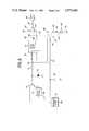
- FIG. 1A typical prior art portable audio product having both a primary load 10 and an auxiliary load 12 is illustrated by FIG. 1.
- the product of FIG. 1also includes a manually operated single pole ON/OFF switch 14 and an automatically operated single pole switch 16 mechanically coupled by suitable actuating means 18 to a line connection apparatus 20 including a jack 22 for receiving one end 23 of an a-c line cord 24.
- the other end of the line cord 24terminates in a plug 28 which may selectively be plugged into an outlet such as a wall receptacle from a source of a-c potential.
- a rectifier 30is coupled to the line connector 20 through a transformer 32, and the output terminal 34 of the rectifier 30 is connected to a first input terminal 36 of the mechanical switch 16.
- 1further includes means 40 for receiving a d-c battery 42 between an output terminal 44 and a common bus or ground 46.
- the output terminal 44is connected to a second input terminal 48 of the mechanical switch 16.
- the switch 16has an output terminal 50 connected in series through the ON/OFF switch 14 to both the primary load 10 and the auxiliary load 12.
- a capacitor 52is provided for smoothing out the d-c voltage supplied to both the primary load 10 and the auxiliary load 12.
- the switches 14 and 16are single pole switches each having a first operative position illustrated by solid lines in FIG. 1 and a second operative position illustrated by broken lines in FIG. 1. More particularly, the ON/OFF switch 14 is manually operated by the consumer. In its first, or ON, position, the switch 14 is closed, and d-c electric power may be supplied therethrough from the output terminal 50 of the switch 16 to both loads. In its second, or OFF, position, the switch 14 is open, and d-c electric power cannot be supplied therethrough to the loads.
- connection 18 between the single pole of the switch 16 and the line connector 20is such that the switch 16 is in its first position connecting the first input terminal 36 and the output terminal 50 whenever the line cord 24 is plugged into the jack 22 and such that the switch 16 is in its second position connecting the second input terminal 48 and the output terminal whenever the line cord 24 is not plugged into the jack 22.
- FIG. 2otherwise, FIGS. 1 and 2 are identical.
- the connection 18may take various forms in practice. In the illustrated form, the connection 18 is merely a mechanical link coupled to a movable member 60 loaded by a compression spring 62. When the connector 23 of the line cord 24 is inserted into the jack 22, it forces the member 60 and thus the pole of the switch 16 to the position illustrated by FIG. 1. When the line cord 24 is removed, the compression spring 62 forces the member 60 and the pole of the switch 16 to the position illustrated by FIG. 2.
- This mechanical operating schemeis intended to be illustrative only; many other arrangements will readily occur to those skilled in the art.
- the switch 16When the connector 23 is inserted into the jack 22, the switch 16 is positioned as shown by FIG. 1. If the plug 28 is attached to a source of a-c potential and the switch 14 is manually placed in its ON position, d-c electric power will be supplied from the output terminal 34 of the rectifier 30 to both the primary load 10 and the auxiliary load 12 through the switches 14 and 16. Power to both loads may be conveniently controlled by means of the ON/OFF switch 14 when the connector 23 is received in the jack 22. If the connector 23 is removed from the jack 22, the pole of the switch 16 will move to its second position (solid line in FIG. 2 and broken line in FIG. 1), and d-c electric power will be supplied from the battery 42 to both the primary load 10 and the auxiliary load 12 through the switches 14 and 16. As indicated previously, this mode of operation may be unsatisfactory because of the large current drain it places on the battery.
- FIG. 3a first preferred embodiment of the present invention is illustrated.
- the primary load 10'is coupled to the output terminal 50' of the switch 16' through the switch 14' in a manner identical to that shown by FIG. 1.
- the auxiliary load 12'is connected in series with the collector and emitter terminals of an NPN transistor 70 to form a load circuit coupled between the switch 14' and the common bus 46'.
- the base or control terminal of the transistor 70is connected through a base resistor 72 to the output terminal 34' of the rectifier 30'.
- a zener diode 74is coupled between the base terminal of the transistor 70 and the common bus 46'.
- the base of the transistor 70When the audio product is powered from an a-c source with the switches 14 and 16 positioned as illustrated by FIG. 3, the base of the transistor 70 is energized as a consequence of its connection to the output terminal 34' of the rectifier 30' through the base resistor 72.
- the value of the base resistor 72is selected to provide sufficient zener current and to turn on the transistor 70.
- the output voltage of the rectifier 30'is also supplied to both the primary load 10' and the load circuit including the auxiliary load 12' through the switches 14' and 16'. As a result, the transistor 70 is turned fully on, and the auxiliary load 12' is energized.
- the voltage across the auxiliary load 12'is maintained substantially constant at a level established by the voltage across the zener diode 74 less the base-emitter junction drop of the transistor 70. If the manual switch 14' is subsequently moved to its OFF position as illustrated by a broken line in FIG. 3, current will no longer flow to the primary load 10' and the collector terminal of the transistor 70. As a result, the primary load 10' will be deenergized and the auxiliary load 12' will be substantially deenergized. A very small current will flow from the rectifier 30' through the base resistor 72 and the base-emitter junction to the auxiliary load 12' and ground.
- the relative values of the rectifier voltage, the base resistor 72 and the auxiliary load 12'are selected such that a current in the order of a very few milliamperes flows from the rectifier 30' to the auxiliary load. This current neither constitutes an appreciable power drain from the a-c source nor results in appreciable energization of the auxiliary load 12'.
- the pole of the switch 16'is moved to the position illustrated by a broken line in FIG. 3.
- the manual ON/OFF switch 14'is thereafter moved to its ON position, the primary load 10' will be powered from the battery 42' through the switches 14' and 16'. Since there is no voltage output from the rectifier 30' at its output terminal 34', however, no current will flow through the base-emitter junction of the transistor 70, and as a consequence the transistor 70 will be non-conductive.
- the auxiliary load 12'is thus not energized when the product is powered from the battery 42'. This result is attained without using multiple pole switches in place of the single pole switches 14 and 16 (FIGS. 1 and 2) of the prior art products.
- FIG. 4A second preferred embodiment of the present invention is illustrated by FIG. 4. This embodiment is similar to the one of FIG. 3, like components being identified by double primed numerals.
- a voltage regulator 80 of conventional formis provided in the circuit between the output terminal 50" of the switch 16" and the primary load 10".
- the voltage regulator 80assures that the primary load 10" is supplied with a substantially constant voltage during operation from either an a-c source or a d-c source.
- the output of the voltage regulator 80is also connected to a load circuit comprising the auxiliary load 12" in series with the collector and emitter terminals of the transistor 70", the emitter terminal being connected to the common bus 46".
- a capacitor 82is provided across the base and emitter junctions of the transistor 70" to smooth out the d-c voltage supplied thereto.
- the transistor 70"when the power cord 24" is connected and the switches 14" and 16" are positioned as illustrated by solid lines, the transistor 70" will be turned on by the current supplied through the base resistor 72".
- the auxiliary load 12"is therefore energized by a substantially constant voltage at a level established by the voltage output of the the voltage regulator 80 less the transistor drop across the collector and emitter terminals. If the switch 14" is switched to its OFF position, current will not flow to the primary and auxiliary loads. Slight current will continue to flow through the base-emitter junction of the transistor 70", but its level will not be appreciable because of the relatively high value of the base resistor 72".
- the switch 16"will shift to the position illustrated by broken lines in FIG. 4, and d-c electric power from the battery 42" will be supplied to the primary load 10" through the switches 14" and 16". Since there is no output voltage from the rectifier 30", however, the transistor 70" will not conduct, and no current will be supplied to the auxiliary load 12".
- the present inventionprovides a consumer electronics product in which both the primary and auxiliary loads are energized in the a-c operating mode, but only the auxiliary load is energized in the d-c operating mode. This result is achieved in a manner that does not require the use of multiple pole switching devices or other costly devices or manufacturing procedures.
Landscapes
- Engineering & Computer Science (AREA)
- Power Engineering (AREA)
- Business, Economics & Management (AREA)
- Emergency Management (AREA)
- Direct Current Feeding And Distribution (AREA)
Abstract
Description
Claims (15)
Priority Applications (1)
| Application Number | Priority Date | Filing Date | Title |
|---|---|---|---|
| US06/660,136US4575640A (en) | 1984-10-12 | 1984-10-12 | Power circuit control apparatus for primary and auxiliary loads |
Applications Claiming Priority (1)
| Application Number | Priority Date | Filing Date | Title |
|---|---|---|---|
| US06/660,136US4575640A (en) | 1984-10-12 | 1984-10-12 | Power circuit control apparatus for primary and auxiliary loads |
Publications (1)
| Publication Number | Publication Date |
|---|---|
| US4575640Atrue US4575640A (en) | 1986-03-11 |
Family
ID=24648304
Family Applications (1)
| Application Number | Title | Priority Date | Filing Date |
|---|---|---|---|
| US06/660,136Expired - LifetimeUS4575640A (en) | 1984-10-12 | 1984-10-12 | Power circuit control apparatus for primary and auxiliary loads |
Country Status (1)
| Country | Link |
|---|---|
| US (1) | US4575640A (en) |
Cited By (21)
| Publication number | Priority date | Publication date | Assignee | Title |
|---|---|---|---|---|
| US4627797A (en)* | 1985-10-15 | 1986-12-09 | Rill Jr Robert W | Standby aquarium pump |
| US4712051A (en)* | 1986-06-02 | 1987-12-08 | Ultima Electronics Ltd. | Adapter for switching from primary to standby device upon failure of primary device |
| US4771184A (en)* | 1986-02-12 | 1988-09-13 | Diehl Gmbh & Co. | Electronic switch apparatus |
| US4871924A (en)* | 1987-12-21 | 1989-10-03 | Sellati Christopher G | Safety power receptacle with hot wire switch-through |
| FR2634569A1 (en)* | 1988-07-19 | 1990-01-26 | Asahi Optical Co Ltd | ELECTRONIC POWER SUPPLY FOR PORTABLE APPARATUS |
| US4908523A (en)* | 1988-04-04 | 1990-03-13 | Motorola, Inc. | Electronic circuit with power drain control |
| US4995017A (en)* | 1987-12-21 | 1991-02-19 | Tec Products, Inc. | Safety power receptacle |
| US5170069A (en)* | 1986-05-21 | 1992-12-08 | Canon Kabushiki Kaisha | Image pickup apparatus |
| US5396107A (en)* | 1991-11-18 | 1995-03-07 | Hitachi, Ltd. | Power source system |
| US5396133A (en)* | 1993-10-01 | 1995-03-07 | Cirrus Logic, Inc. | High speed CMOS current switching circuits |
| US5425278A (en)* | 1993-09-17 | 1995-06-20 | Pneumatic Scale Corporation | Weigh scale with sapphire load cell |
| US5753980A (en)* | 1996-04-25 | 1998-05-19 | Thomson Consumer Electronics, Inc. | Automatic prevention of inadvertent operation of electronic devices |
| US5872433A (en)* | 1986-05-21 | 1999-02-16 | Canon Kabushiki Kaisha | Image pickup apparatus including interruption means for causing recordation of an electrical image signal in response to operation of a second trigger before completion of a predetermined step by a first trigger |
| US5892393A (en)* | 1995-03-29 | 1999-04-06 | Nec Corporation | Power supply circuit having an auxiliary power source for compensating for main power drop |
| US20040046458A1 (en)* | 2002-08-22 | 2004-03-11 | Robin Mackay | Precise power system |
| US20040128085A1 (en)* | 2002-09-12 | 2004-07-01 | Ramirez Anibal Diego | Electricity meter with power supply load management |
| US7558083B2 (en) | 1997-01-24 | 2009-07-07 | Synqor, Inc. | High efficiency power converter |
| US7564702B2 (en) | 1997-01-24 | 2009-07-21 | Synqor, Inc. | High efficiency power converter |
| WO2013019659A1 (en)* | 2011-07-29 | 2013-02-07 | Adt Us Holding, Inc. | Security system and method |
| US10199950B1 (en) | 2013-07-02 | 2019-02-05 | Vlt, Inc. | Power distribution architecture with series-connected bus converter |
| US11536754B2 (en) | 2019-08-15 | 2022-12-27 | Landis+Gyr Innovations, Inc. | Electricity meter with fault tolerant power supply |
Citations (5)
| Publication number | Priority date | Publication date | Assignee | Title |
|---|---|---|---|---|
| US3562555A (en)* | 1967-09-01 | 1971-02-09 | Rca Corp | Memory protecting circuit |
| US4054802A (en)* | 1976-10-04 | 1977-10-18 | General Motors Corporation | Power control circuit |
| US4327298A (en)* | 1979-12-14 | 1982-04-27 | Borg-Warner Corporation | Battery backup system for a microcomputer |
| US4375701A (en)* | 1980-07-17 | 1983-03-01 | General Electric Company | Battery or AC driven radio receiver power supply |
| US4486759A (en)* | 1981-06-30 | 1984-12-04 | Canon Kabushiki Kaisha | Electronic equipment |
- 1984
- 1984-10-12USUS06/660,136patent/US4575640A/ennot_activeExpired - Lifetime
Patent Citations (5)
| Publication number | Priority date | Publication date | Assignee | Title |
|---|---|---|---|---|
| US3562555A (en)* | 1967-09-01 | 1971-02-09 | Rca Corp | Memory protecting circuit |
| US4054802A (en)* | 1976-10-04 | 1977-10-18 | General Motors Corporation | Power control circuit |
| US4327298A (en)* | 1979-12-14 | 1982-04-27 | Borg-Warner Corporation | Battery backup system for a microcomputer |
| US4375701A (en)* | 1980-07-17 | 1983-03-01 | General Electric Company | Battery or AC driven radio receiver power supply |
| US4486759A (en)* | 1981-06-30 | 1984-12-04 | Canon Kabushiki Kaisha | Electronic equipment |
Cited By (43)
| Publication number | Priority date | Publication date | Assignee | Title |
|---|---|---|---|---|
| US4627797A (en)* | 1985-10-15 | 1986-12-09 | Rill Jr Robert W | Standby aquarium pump |
| US4771184A (en)* | 1986-02-12 | 1988-09-13 | Diehl Gmbh & Co. | Electronic switch apparatus |
| US5872433A (en)* | 1986-05-21 | 1999-02-16 | Canon Kabushiki Kaisha | Image pickup apparatus including interruption means for causing recordation of an electrical image signal in response to operation of a second trigger before completion of a predetermined step by a first trigger |
| US6947081B2 (en) | 1986-05-21 | 2005-09-20 | Canon Kabushiki Kaisha | Image pickup apparatus having means to control adjustment of color balance based on image pickup mode |
| US5170069A (en)* | 1986-05-21 | 1992-12-08 | Canon Kabushiki Kaisha | Image pickup apparatus |
| US20040201716A1 (en)* | 1986-05-21 | 2004-10-14 | Canon Kabushiki Kaisha | Image pickup apparatus having means to control adjustment of color balance based on image pickup mode |
| US6266083B1 (en) | 1986-05-21 | 2001-07-24 | Canon Kabushiki Kaisha | Image pickup apparatus including interruption means for causing recordation of an electrical image signal in response to operation of a second trigger before completion of a predetermined step by a first trigger |
| US4712051A (en)* | 1986-06-02 | 1987-12-08 | Ultima Electronics Ltd. | Adapter for switching from primary to standby device upon failure of primary device |
| US4871924A (en)* | 1987-12-21 | 1989-10-03 | Sellati Christopher G | Safety power receptacle with hot wire switch-through |
| US4995017A (en)* | 1987-12-21 | 1991-02-19 | Tec Products, Inc. | Safety power receptacle |
| US4908523A (en)* | 1988-04-04 | 1990-03-13 | Motorola, Inc. | Electronic circuit with power drain control |
| US4920307A (en)* | 1988-07-19 | 1990-04-24 | Asahi Kogaku Kogyo Kabushiki Kaisha | Electric power source used to charge a secondary power source |
| FR2634569A1 (en)* | 1988-07-19 | 1990-01-26 | Asahi Optical Co Ltd | ELECTRONIC POWER SUPPLY FOR PORTABLE APPARATUS |
| US5396107A (en)* | 1991-11-18 | 1995-03-07 | Hitachi, Ltd. | Power source system |
| US5425278A (en)* | 1993-09-17 | 1995-06-20 | Pneumatic Scale Corporation | Weigh scale with sapphire load cell |
| US5396133A (en)* | 1993-10-01 | 1995-03-07 | Cirrus Logic, Inc. | High speed CMOS current switching circuits |
| US5892393A (en)* | 1995-03-29 | 1999-04-06 | Nec Corporation | Power supply circuit having an auxiliary power source for compensating for main power drop |
| US5753980A (en)* | 1996-04-25 | 1998-05-19 | Thomson Consumer Electronics, Inc. | Automatic prevention of inadvertent operation of electronic devices |
| US9143042B2 (en) | 1997-01-24 | 2015-09-22 | Synqor, Inc. | High efficiency power converter |
| US8493751B2 (en) | 1997-01-24 | 2013-07-23 | Synqor, Inc. | High efficiency power converter |
| US7558083B2 (en) | 1997-01-24 | 2009-07-07 | Synqor, Inc. | High efficiency power converter |
| US8023290B2 (en) | 1997-01-24 | 2011-09-20 | Synqor, Inc. | High efficiency power converter |
| US20100091526A1 (en)* | 1997-01-24 | 2010-04-15 | Schlecht Martin F | High efficiency power converter |
| US7564702B2 (en) | 1997-01-24 | 2009-07-21 | Synqor, Inc. | High efficiency power converter |
| US6977446B2 (en)* | 2002-08-22 | 2005-12-20 | Robin Mackay | Multiple inverter power system with regard to generator failure |
| US20040046458A1 (en)* | 2002-08-22 | 2004-03-11 | Robin Mackay | Precise power system |
| US7348769B2 (en) | 2002-09-12 | 2008-03-25 | Landis+Gyr, Inc. | Electricity meter with power supply load management |
| US7135850B2 (en) | 2002-09-12 | 2006-11-14 | Landis+Gyr, Inc. | Electricity meter with power supply load management |
| US20060158177A1 (en)* | 2002-09-12 | 2006-07-20 | Landis+Gyr, Inc.. | Electricity meter with power supply load management |
| US20060145685A1 (en)* | 2002-09-12 | 2006-07-06 | Landis+Gyr, Inc. | Electricity meter with power supply load management |
| US7009379B2 (en) | 2002-09-12 | 2006-03-07 | Landis & Gyr, Inc. | Electricity meter with power supply load management |
| US20040128085A1 (en)* | 2002-09-12 | 2004-07-01 | Ramirez Anibal Diego | Electricity meter with power supply load management |
| US9117349B2 (en) | 2011-07-29 | 2015-08-25 | Adt Us Holdings, Inc. | Security system having segregated operating software |
| US8665084B2 (en) | 2011-07-29 | 2014-03-04 | Adt Us Holdings, Inc. | Security system and method |
| WO2013019659A1 (en)* | 2011-07-29 | 2013-02-07 | Adt Us Holding, Inc. | Security system and method |
| US9286772B2 (en) | 2011-07-29 | 2016-03-15 | Adt Us Holdings, Inc. | Security system and method |
| US9589441B2 (en) | 2011-07-29 | 2017-03-07 | Adt Us Holdings, Inc. | Security system and method |
| US10199950B1 (en) | 2013-07-02 | 2019-02-05 | Vlt, Inc. | Power distribution architecture with series-connected bus converter |
| US10594223B1 (en) | 2013-07-02 | 2020-03-17 | Vlt, Inc. | Power distribution architecture with series-connected bus converter |
| US11075583B1 (en) | 2013-07-02 | 2021-07-27 | Vicor Corporation | Power distribution architecture with series-connected bus converter |
| US11705820B2 (en) | 2013-07-02 | 2023-07-18 | Vicor Corporation | Power distribution architecture with series-connected bus converter |
| US12395087B1 (en) | 2013-07-02 | 2025-08-19 | Vicor Corporation | Power distribution architecture with series-connected bus converter |
| US11536754B2 (en) | 2019-08-15 | 2022-12-27 | Landis+Gyr Innovations, Inc. | Electricity meter with fault tolerant power supply |
Similar Documents
| Publication | Publication Date | Title |
|---|---|---|
| US4575640A (en) | Power circuit control apparatus for primary and auxiliary loads | |
| US5270576A (en) | Electrical connector network | |
| US4044268A (en) | Multiple power source automatic switching circuitry | |
| US4608500A (en) | Electric power unit | |
| US4054802A (en) | Power control circuit | |
| JP2649950B2 (en) | Power supply | |
| US4398098A (en) | Electronic latching circuit | |
| US5962932A (en) | Power supply apparatus with circuit load sensor | |
| US4380809A (en) | Automatic power supply system | |
| US5028862A (en) | Voltage follower circuit for use in power level control circuits | |
| JPH02294277A (en) | Initial power-up equipment for switching power supply equipment | |
| US3898474A (en) | Power circuit | |
| GB2223893A (en) | Oscillator circuit for lighting supply | |
| US4051547A (en) | Solid state relay | |
| US5345360A (en) | Switched receptacle circuit | |
| KR200256172Y1 (en) | AC/DC Multi-tap | |
| US3049591A (en) | Electronic system | |
| KR19980015556A (en) | Power supply control circuit and power supply control method to electronic microcomputer | |
| JP2543543B2 (en) | 2-wire wiring equipment | |
| KR810002078B1 (en) | Power circuit | |
| JP2690185B2 (en) | Power supply circuit | |
| KR870001301Y1 (en) | Power circuit | |
| KR200296292Y1 (en) | Power control device | |
| KR880002086Y1 (en) | Imager power switching circuit of audio / video controller | |
| KR0141327B1 (en) | Ac/dc automatic converting circuits |
Legal Events
| Date | Code | Title | Description |
|---|---|---|---|
| AS | Assignment | Owner name:GENERAL ELECTRIC COMPANY A CORP OF NEW YORK Free format text:ASSIGNMENT OF ASSIGNORS INTEREST.;ASSIGNOR:MARTIN, HUGH H.;REEL/FRAME:004325/0417 Effective date:19841008 | |
| FEPP | Fee payment procedure | Free format text:PAYOR NUMBER ASSIGNED (ORIGINAL EVENT CODE: ASPN); ENTITY STATUS OF PATENT OWNER: LARGE ENTITY Free format text:PAYER NUMBER DE-ASSIGNED (ORIGINAL EVENT CODE: RMPN); ENTITY STATUS OF PATENT OWNER: LARGE ENTITY | |
| STCF | Information on status: patent grant | Free format text:PATENTED CASE | |
| PA | Patent available for licence or sale | ||
| AS | Assignment | Owner name:RCA LICENSING CORPORATION, TWO INDEPENDECE WAY, PR Free format text:ASSIGNMENT OF ASSIGNORS INTEREST.;ASSIGNOR:GENERAL ELECTRIC COMPANY, A NY CORP.;REEL/FRAME:004854/0730 Effective date:19880126 Owner name:RCA LICENSING CORPORATION, A DE CORP.,NEW JERSEY Free format text:ASSIGNMENT OF ASSIGNORS INTEREST;ASSIGNOR:GENERAL ELECTRIC COMPANY, A NY CORP.;REEL/FRAME:004854/0730 Effective date:19880126 | |
| FPAY | Fee payment | Year of fee payment:4 | |
| FEPP | Fee payment procedure | Free format text:PAYER NUMBER DE-ASSIGNED (ORIGINAL EVENT CODE: RMPN); ENTITY STATUS OF PATENT OWNER: LARGE ENTITY | |
| FPAY | Fee payment | Year of fee payment:8 | |
| FPAY | Fee payment | Year of fee payment:12 |