US4571819A - Method for forming trench isolation structures - Google Patents
Method for forming trench isolation structuresDownload PDFInfo
- Publication number
- US4571819A US4571819AUS06/667,181US66718184AUS4571819AUS 4571819 AUS4571819 AUS 4571819AUS 66718184 AUS66718184 AUS 66718184AUS 4571819 AUS4571819 AUS 4571819A
- Authority
- US
- United States
- Prior art keywords
- layer
- trench
- oxide
- forming
- etch
- Prior art date
- Legal status (The legal status is an assumption and is not a legal conclusion. Google has not performed a legal analysis and makes no representation as to the accuracy of the status listed.)
- Expired - Lifetime
Links
Images


Classifications
- H—ELECTRICITY
- H01—ELECTRIC ELEMENTS
- H01L—SEMICONDUCTOR DEVICES NOT COVERED BY CLASS H10
- H01L21/00—Processes or apparatus adapted for the manufacture or treatment of semiconductor or solid state devices or of parts thereof
- H01L21/70—Manufacture or treatment of devices consisting of a plurality of solid state components formed in or on a common substrate or of parts thereof; Manufacture of integrated circuit devices or of parts thereof
- H01L21/71—Manufacture of specific parts of devices defined in group H01L21/70
- H01L21/76—Making of isolation regions between components
- H01L21/762—Dielectric regions, e.g. EPIC dielectric isolation, LOCOS; Trench refilling techniques, SOI technology, use of channel stoppers
- H01L21/76224—Dielectric regions, e.g. EPIC dielectric isolation, LOCOS; Trench refilling techniques, SOI technology, use of channel stoppers using trench refilling with dielectric materials
- Y—GENERAL TAGGING OF NEW TECHNOLOGICAL DEVELOPMENTS; GENERAL TAGGING OF CROSS-SECTIONAL TECHNOLOGIES SPANNING OVER SEVERAL SECTIONS OF THE IPC; TECHNICAL SUBJECTS COVERED BY FORMER USPC CROSS-REFERENCE ART COLLECTIONS [XRACs] AND DIGESTS
- Y10—TECHNICAL SUBJECTS COVERED BY FORMER USPC
- Y10S—TECHNICAL SUBJECTS COVERED BY FORMER USPC CROSS-REFERENCE ART COLLECTIONS [XRACs] AND DIGESTS
- Y10S148/00—Metal treatment
- Y10S148/043—Dual dielectric
- Y—GENERAL TAGGING OF NEW TECHNOLOGICAL DEVELOPMENTS; GENERAL TAGGING OF CROSS-SECTIONAL TECHNOLOGIES SPANNING OVER SEVERAL SECTIONS OF THE IPC; TECHNICAL SUBJECTS COVERED BY FORMER USPC CROSS-REFERENCE ART COLLECTIONS [XRACs] AND DIGESTS
- Y10—TECHNICAL SUBJECTS COVERED BY FORMER USPC
- Y10S—TECHNICAL SUBJECTS COVERED BY FORMER USPC CROSS-REFERENCE ART COLLECTIONS [XRACs] AND DIGESTS
- Y10S148/00—Metal treatment
- Y10S148/05—Etch and refill
- Y—GENERAL TAGGING OF NEW TECHNOLOGICAL DEVELOPMENTS; GENERAL TAGGING OF CROSS-SECTIONAL TECHNOLOGIES SPANNING OVER SEVERAL SECTIONS OF THE IPC; TECHNICAL SUBJECTS COVERED BY FORMER USPC CROSS-REFERENCE ART COLLECTIONS [XRACs] AND DIGESTS
- Y10—TECHNICAL SUBJECTS COVERED BY FORMER USPC
- Y10S—TECHNICAL SUBJECTS COVERED BY FORMER USPC CROSS-REFERENCE ART COLLECTIONS [XRACs] AND DIGESTS
- Y10S148/00—Metal treatment
- Y10S148/133—Reflow oxides and glasses
Definitions
- This inventionrelates to techniques for electrically isolating semiconductor devices and components in monolithic integrated circuits.
- the inventionis a method for forming void-free, planarized dielectric trench structures.
- the methoduses doped oxide reflow to provide a void-free planar isolation layer and a multiple underlayer which functions as an etch stop and dopant/oxidation barrier.
- Dielectric isolation techniqueshave been the preferred technology for isolating integrated circuits and their constituent devices and elements, at least in part because of the ability to closely pack the isolation dielectric and the circuit elements.
- Integrated circuit isolation by the so-called local oxidation of silicon (LOCOS)has been known for a number of years, as have the attendant problems.
- LOCOSlocal oxidation of silicon
- the well-known limitations of the LOCOS processinclude at least three factors which may constrain the process from applicability to future small geometry, highly dense LSI and VLSI structures. These limitations are, first, the formation of the so-called bird's beak oxide configuration and the associated encroachment of the field oxide beneath the oxidation mask. Encroachment by the bird's beak oxide limits the percentage of chip surface area which is available for device formation.
- the limited thicknessresults in undesirably high circuit capacitances.
- the characteristic non-planar surface topographymakes it difficult to perform the increasingly high resolution photolithographic operations which are required to fabricate VSLI circuits.
- the decreased resolutionincreases the minimum feature sizes and minimum tolerances and, as a consequence, decreases the achievable device densities.
- LOCOS isolationhas persisted, however, because of the past shortcomings of the available substitute isolation technologies.
- Typical trench isolation processesinvolve etching grooves about 1 to 6 microns deep into the semiconductor substrate, filling the grooves with a suitable dielectric and performing a planarization operation.
- the dielectric materialtypically is undoped silicon dioxide or polysilicon.
- Typical prior art approachesare discussed, for example, in Rung, Momose and Nagakubo, "Deep Trench Isolated CMOS Devices", IEDM 82, pp. 237-240. The Rung et al.
- trench isolation technologyhas the inherent potential advantages of small width-to-depth ratios, relative process simplicity, well-defined vertical-wall isolation regions and surface planarity.
- the width of isolation trenchesmust be scaled downward to near micron and even submicron size to achieve the densities required in VSLI and future monolithic integrated circuit technologies.
- the resulting tendency to form voidsis well-known and is shown, for example, by the data of Bondur et al, U.S. Pat. No. 4,104,086. Bondur et al.
- FIG. 1illustrates the data of Bondur et al., which show that for vertical side wall trenches, the deposited silicon dioxide forms negative sloping side walls and, thus, voids.
- RisemanU.S. Pat. No. 4,356,211, forms a composite dual-oxide trench isolation structure in which a first oxide layer is formed, then a layer of polysilicon is deposited, anisotrophically etched, and heavily doped at the upper edge of the trench to accelerate silicon dioxide formation at such upper edge. Thereby the voids are sealed by the differential oxidation rate of the polysilicon.
- the parameters of the Riseman processdo not provide for applications in which trenches of varying dimension are being processed simultaneously.
- the above-mentioned Bondur et al. U.S. Pat. No. 4,104,086uses tapered trench sidewalls to control the depth of isolation oxide voids relative to the substrate surface in a silicon substrate which has a highly doped near-surface region.
- the Bondur et al processinvolves (1) forming the trench to a tapered profile, as by the use of reactive ion etching (RIE); (2) growing a thin layer of thermal oxide in the trench outline; (3) depositing CVD oxide; (4) etching back the CVD oxide using RIE; and (5) optionally, annealing in steam at 900° to 950° C. to enhance the "quality" of the silicon dioxide.
- RIEreactive ion etching
- the data disclosed in the Bondur et al patentindicate the vertical walls (which, of course, are desirable for density and resolution) inherently product voids in the deposited silicon oxide (see FIG. 1 herein). Also, the voids are buried deeper in the oxide relative to the substrate surface as the trench width increases and the taper increases. Conversely, the voids are formed closer to the surface and to exposure by the planarization etch-back in the case of narrower, vertical grooves.
- SakuraiU.S. Pat. No. 4,404,735, discloses a process for forming trench isolation structures. Initially, dry etching such as plasma etching, reactive sputter etching or ion beam etching is used for form the trench. The trench is then covered with a thin layer of deposited silicon dioxide which is formed to a thickness of between 500 to 1,000 angstroms to prevent substrate heating by the subsequent laser reflow process, prevent doping of the substrate from the isolation layer, and to isolate the silicon isolation layer from the substrate. Next, a CVD layer is formed to a thickness which is less than the trench depth and less than one-half the trench width using silicon or doped glass (phosphosilicate glass, PSG). The PSG/silicon is subsequently reflowed by laser heating.
- dry etchingsuch as plasma etching, reactive sputter etching or ion beam etching is used for form the trench.
- the trenchis then covered with a thin layer of deposited silicon dioxide which is formed to a thickness of between 500
- the Sakurai processis a laser reflow process for filling narrow trenches from a thin silicon or PSG layer.
- the trench-filling layeris formed to an initial shallow thickness within the trench and laser heating is used to redistribute material from outside the trenches into the trenches.
- the 500 to 1,000 Angstrom thickness of the blocking silicon dioxide layeris critical in that a minimum thickness is required to perform the heat-shielding and dopant-blocking functions, while, presumably, a maximum thickness is necessary for consistency with the state depth and width dimensions.
- Another object of the present inventionis to provide a method for forming such a trench isolation structure which has planar surface topography over the trenches as well as the active regions.
- Still another object of the present inventionis to provide a process for forming void-free trench isolation structures which are suitable for use in high density monolithic integrated circuit structures such as VLSI circuits.
- the method of the present inventioncomprises the steps of forming, in a substrate, a trench which has substantially vertical sidewalls; forming a thin, stress relief oxide layer in the trench outline; forming an etch-stop buffer layer in the trench outline; forming a dopant-blocking and oxidation blocking layer in the trench outline; forming a doped dielectric isolation layer on the structure; heating the resulting structure to reflow the dielectric collapse voids therein and smooth the outer surface of the isolation layer; etching the dielectric isolation layer to a level at or below the etch-stop buffer layer; heating the structure for a time sufficient to outgas the dopant, while at the same time such blocking layer prevents diffusion of the dopant into the underlying structure; and selectively etching the etch-stop buffer layer, as required, preparatory to further IC fabrication.
- a polymer such as PMMApolymethylmethacylate
- PMMApolymethylmethacylate
- the stress relief layeris thermal oxide which is 300 to 1,000 Angstroms thick.
- the etch-stop layeris deposited polycrystalline silicon (polysilicon) which is 1,000 to 3,000 Angstroms thick.
- the blocking layeris silicon nitride formed to a thickness of 1,000 to 3,000 Angstroms thick to prevent doping and oxidation of the underlying polysilicon and other structural layers.
- the dielectric isolation layeris chemical vapor deposited (CVD) silicon oxide approximately 2.5 microns thick which contains approximately 3 to 9 weight percent dopants such as phosphorus or boron to provide the requisite reflow characteristics. Reflow itself is done at 950° to 1,150° C.
- the etch-back and selective etchcan be done by conventional RIE techniques.
- the outgassing stepinvolves heating at about 1,000° to 1,200° C. in a nitrogen ambient for two to eight hours to deplete the dielectric surface of dopant and, optionally, to drive in surface adjacent diffusion regions such as the p/n wells used in CMOS integrated circuits.
- the polysilicon etch stop layeris formed on the silicon nitride blocking layer, rather than vice versa.
- This approacheliminates possible interaction between the glass isolation layer and the nitride, which can occur when the nitride is formed on the polysilicon.
- an oxidizing reflow ambientis not used with this poly-on-nitride configuration, because the resulting polysilicon oxidation can consume the poly etch stop layer.
- a poly-nitride-poly-oxide sequence of layerscan be used.
- the outermost poly layer in this configurationacts as a passivation barrier over the nitride to eliminate nitride reaction with the glass isolation layer.
- oxidation of the polyhelps to fill in the trench.
- the nitrideblocks oxidation of the innermost poly layer during reflow and limits any poly consumption to the outermost poly layer. In blocking oxidation of the innermost poly layer, the nitride permits the use of an oxidizing reflow ambient.
- FIG. 1illustrates prior art data which demonstrates that formation of dielectric such as silicon dioxide in vertical sidewall trenches produces a negatively sloped dielectric walls and voids.
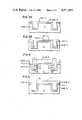
- FIGS. 2 through 7are cross-sectional representations of a preferred process for fabricating the void-free silicon dioxide composite trench isolation structures of the present invention.
- FIG. 3A and 3Bare cross-sectional representations of alternative composite structures which may be used in the structure and process of the present invention.
- FIG. 8is an exemplary IC structure based upon the trench isolation process and structure of the present invention.
- the present inventionis a trench isolation technology which utilizes the reflow characteristics of doped silica glass at elevated temperatures to compensate for the tendency for form voids in the trenches of varying dimensions which are required for small geometry, high-density, monolithic integrated circuits.
- the processtherby provides a high-quality, void-free planar trench isolation structure.
- the use of reflowed doped silica glassis made possible by the preliminary formation of a silicon nitride barrier layer which prevents doping and oxidation of the underlying structure, particularly the semiconductor substrate; and underlying polysilicon layer which provides an etch-stop during the oxide planarization etchback; and an underlying silicon oxide layer which decreases stress in the novel four-layer composite trench structure.
- the processis believed unique in its approach to the use of vertical sidewalls in trench structures of various widths. These vertical sidewalls minimize the effective wafer area allocated to the trenches. In addition, the process results in a planar wafer surface suitable for use with high resolution photolithography. Foremost, these objectives are obtained through the use of conventional fabrication techniques, and without imposing elaborate trench shape or dimensional controls.
- a semiconductor substrate 10typically of silicon.
- the substratewould be p - silicon having a resistivity of 1 to 20 ohms - centimeter.
- a typical CMOS starting structurewould be an n - epitaxial layer on an n+ substrate.
- the substrate 10can be masked using any of a number and combinations thereof, as well as by the exemplary photoresist mask which is shaped by exposure to ultraviolet radiation.
- mask compositions suitable for X-Ray or ion beam exposurecan be used.
- photoresista layer thereof is formed on the substrate 10, then is exposed and developed to produce the etch mask 11 which has openings 12 corresponding to the desired trench width. Note that the dimensions of the drawings herein are chosen for convenience of representation, are not to scale, and according to the invention are subject to variation.
- the trenchis etched to a typical depth of 1 to 6 microns, preferably using an anisotropic etch process to produce a trench 13 having vertical sidewalls 14-14.
- One preferred etch processis reactive ion etching using a fluorine etchant gas such as nitrogen trifluoride (NF 3 ).
- NF 3nitrogen trifluoride
- the mechanical component or ion bombardment component 15dominates the chemical reaction component and provides the vertical sidewalls which are desirable in order to provide sufficient dielectric width for effective isolation without lateral encroachment into active device regions.
- a stress relief oxide layer 16is formed to a thickness of about 300 to 1,000 Angstroms by thermal oxidation in steam at 950° to 1,150° C., or by chemical vapor deposition (CVD).
- the oxide layer 16provides stress relief between the silicon substrate 10 and the overlying layer, in this instance a polycrystalline silicon etch-stop layer 17 which is formed to a thickness of about 1,000 to 3,000 Angstroms, for example, by the LPCVD technique (low pressure chemical vapor deposition) using silane in argon and hydrogen at 600°-800° C.
- the poly layer 17prevents etching of the underlying structure, particularly the substrate, during the planarization process.
- the primary purpose of the oxide layer 16is stress relief of the substrate 10, to preserve the electrical integrity of the substrate.
- the silicon nitride barrier layer 18is then formed to a thickness of 1,000 to 2,500 Angstroms on the polysilicon layer 17, preferably by low pressure chemical vapor deposition using silane and ammonia and a reaction temperature of about 800° C.
- the silicon nitride layer 18provides a barrier to doping and oxidation of the underlying structure, particularly substrate 10, during subsequent processing. Thereby, silicon nitride layer 18 permits formation and reflow of the doped isolation oxide and subsequent outgassing of the dopant in the isolation oxide without affecting the substrate or polysilicon or the rest of the underlying structure.
- the doped silicon dioxide glass layer 19can be formed to a thickness of about 2.5 microns containing 3-9 weight percent of impurities such as phosphorus or boron, e.g., using the low pressure chemical vapor deposition technique.
- impuritiessuch as phosphorus or boron
- the reactants silane and oxygenare used, with phosphine as the n-type dopant, and a reaction temperature of about 500°-800° C.
- the resulting silicon dioxide layer 19includes voids 21-21, which is typical when silicon dioxide or other dielectric layers are formed in deep trenches.
- the voidsoccur because the arrival angles of the depositing silicon dioxide at the botton 22 and sidewalls 14-14 of the trench are small in comparison to the arrival angle at the top edges 23-23 of the trench.
- Thisproduces relatively low deposition growth rates at the bottom and sides in comparison to the top and edge.
- the deposition rate differentialproduces the negatively sloped sidewalls which are evidenced by the data of FIG. 1, with the result that the fast growing oxide in the edge regions 23-23 closes up the opening of the trench before the bottom regions are filled.
- the resulting voids 21-21are not filled in by subsequent oxide growth or by the application of planarization materials such as polymer layers.
- the voidswould be exposed during the subsequent etchback which is used to planarize the doped glass, creating an open receptacle for process chemical or impurities and allowing subsequently deposited metallization to flow into the voids and short other devices and components along the trench.
- the doped glassis melted and reflowed by applying a temperature of about 950° to 1,150° C. in steam (oxidizing) or nitrogen (non-oxidizing) ambient for about 30 minutes to four hours depending upon the glass thickness and the trench dimensions. See FIG. 5.
- the range of timesresults from the faster reflow which occurs as the process temperature is increased and from the requirement of longer processing times for thicker silicon dioxide layers 19.
- This processcollapses the voids 21-21 and, for trench width dimensions of up to about 5 microns, reflows the upper surface 26 of the glass to a substantially level topography.
- the silicon nitride layer 18provides a barrier to oxidation and doping of the underlying polysilicon layer 17.
- planarizationis aided by depositing after the reflow a layer 27 of polymer such as PMMA to a thickness which is appropriate to the particular trench depth and width being used. It should be noted that one of the advantages of the present process is its adaptability to a wide range of trench dimensions, e.g., trench widths of one micron to 50 microns. According to this embodiment, planarization of the underlying glass is carried out by using an etch which removes PMMA and glass at substantially equal rates.
- the silicon dioxide isolation layer 19is etched back so that the surface 28 of the resulting glass field isolation regions 19-19 of the trench structure 29-29 is level with or below the surface of the polysilicon etch-stop/buffer layer 17.
- the etchcan be done using a selective wet chemical etchant such as buffered hydrogen fluoride, or using dry etching such as reactive ion etching with CHF 3 etchant gas.
- a selective wet chemical etchantsuch as buffered hydrogen fluoride
- dry etchingsuch as reactive ion etching with CHF 3 etchant gas.
- the use of an RIE oxide etchalso removes the silicon nitride layer 18 outside the trench confines.
- the optional polymer layerhas been used, it can be removed using the same reactive ion etching process which is applied to remove the silicon dioxide.
- the etchant useddoes not attack poly, so that the polymer 27, oxide 19 and nitride 18 can be etched using the poly as an
- the next stepis to outgas the phosphorus or boron dopant from the trench oxide 19-19 at a temperature of about 1,000° to 1,200° C. in a nitrogen ambient for about two to eight hours.
- This stepdepletes the surface of the glass of the dopant and may also be used, for example, for the well drive-in of CMOS integrated circuits.
- the silicon nitride layeragain serves as a barrier to prevent doping or oxidation of the underlying trench structure including the substrate. It is no doubt recognized that even small amounts of dopant diffused through the barrier into silicon substrate 10 create parasitic current leakage paths.
- the polysilicon layer 17is removed from the active regions such as 31-31.
- the polysiliconcan be removed using reactive ion etching or by wet chemical etching. Standard integrated circuit processing may then proceed.
- the resulting trench structures 29-29 shown in FIG. 7form the narrow, yet relatively deep, vertical sidewall, void-free structures which are necessary for small geometry, high-density, integrated circuits.
- the silicon nitride blocking layer 18, the polysilicon etch-stop/buffer layer 17 and the stress relief oxide layer 16remain in place and contribute to the dielectric isolation. Foremost, the structure is created without critical reliance on exotic equipment or highly refined trench shape control procedures.
- the polysilicon etch-stop layer 47is formed on the silicon nitride blocking layer 48, rather than vice versa.
- This poly-overnitride approacheliminates possible interaction between the glass isolation layer 19 and the nitride, which can occur when the nitride is formed on the poly (see FIGS. 3 and 4).
- an oxidizing reflow ambientis not used with the poly-on-nitride configuration of FIG. 3A, because the resulting polysilicon oxidation can consume the poly etch-stop layer 17.
- the fabrication process for the poly-nitride-oxide composite of FIG. 3Ais similar to that described relative to the nitride-poly-oxide composite of FIG. 3 with the exception that the nitride 48 is under the poly etch-stop layer 47 and thus typically cannot be removed during the etch back of glass 19. Instead, the etching sequence is glass 19, poly 47 and then nitride 48.
- the poly 47, nitride 48 and oxide 16 of FIG. 3Aperform the same functions--etch-stop, oxidation and dopant blocking, and stress relief--as do the poly 17, nitride 18 and oxide 16 of FIG. 3.
- a poly-nitride-poly-oxide sequence of layersis used.
- the outermost poly layer 47acts as a barrier for the nitride 18 to eliminate any nitride reaction with the glass isolation layer 19, e.g., during the oxide reflow.
- oxidation of the poly 47helps fill in and level the trench structures.
- the nitride 18in turn blocks oxidation of the innermost poly layer 17 and thereby limits any poly consumption during the reflow step to the outermost poly layer 47.
- the nitride layer 18preserves the innermost poly layer 17 and permits the use of an oxidizing ambient during reflow.
- the nitride 18 and poly 17perform the same respective oxidation and dopant blocking and etch-stop functions as do the nitride 18 and poly 17 in FIG. 3.
- the fabrication process for the polynitride-poly-oxide composite structureinvolves obvious modifications of the nitride-poly fabrication of FIG. 3, involving primarily the addition of a second poly CVD step.
- the glass 19, poly 47, nitride 18 and poly 17 layersare removed sequentially. If the poly 47 is totally consumed during the reflow, the removal sequence for the FIG. 3 structure can be used.
- FIG. 8there is shown one example of a MOSFET structure based upon the trench isolation structures 29 of the present invention.
- an NMOS FET of a complementary structureis shown formed in the p-well 33 of an n-type epitaxial layer 34.
- the FETincludes source and drain diffusions 36 and 37 and LDD implants 38, all of which are self-aligned with the polysilicon gate 39, as well as gate sidewall spacers 41, interlevel dielectric 42 and aluminum interconnects 43. Quite obviously, this is only one possible application among the various NMOS, PMOS, CMOS, bipolar and other applications of the present trench isolation structure and process.
Landscapes
- Engineering & Computer Science (AREA)
- Physics & Mathematics (AREA)
- Condensed Matter Physics & Semiconductors (AREA)
- General Physics & Mathematics (AREA)
- Manufacturing & Machinery (AREA)
- Computer Hardware Design (AREA)
- Microelectronics & Electronic Packaging (AREA)
- Power Engineering (AREA)
- Element Separation (AREA)
Abstract
Description
Claims (16)
Priority Applications (7)
| Application Number | Priority Date | Filing Date | Title |
|---|---|---|---|
| US06/667,181US4571819A (en) | 1984-11-01 | 1984-11-01 | Method for forming trench isolation structures |
| US06/783,717US4656497A (en) | 1984-11-01 | 1985-10-03 | Trench isolation structures |
| EP85905690AEP0200771B1 (en) | 1984-11-01 | 1985-10-28 | Process for forming isolation regions in a semiconductor substrate |
| DE8585905690TDE3571893D1 (en) | 1984-11-01 | 1985-10-28 | Process for forming isolation regions in a semiconductor substrate |
| DE1985905690DE200771T1 (en) | 1984-11-01 | 1985-10-28 | METHOD FOR PRODUCING INSULATION ZONES IN A SEMICONDUCTOR SUBSTRATE. |
| PCT/US1985/002119WO1986002777A1 (en) | 1984-11-01 | 1985-10-28 | Process for forming isolation regions in a semiconductor substrate |
| JP60505028AJPH0685413B2 (en) | 1984-11-01 | 1985-10-28 | Method for forming insulating region on semiconductor substrate |
Applications Claiming Priority (1)
| Application Number | Priority Date | Filing Date | Title |
|---|---|---|---|
| US06/667,181US4571819A (en) | 1984-11-01 | 1984-11-01 | Method for forming trench isolation structures |
Related Child Applications (1)
| Application Number | Title | Priority Date | Filing Date |
|---|---|---|---|
| US06/783,717DivisionUS4656497A (en) | 1984-11-01 | 1985-10-03 | Trench isolation structures |
Publications (1)
| Publication Number | Publication Date |
|---|---|
| US4571819Atrue US4571819A (en) | 1986-02-25 |
Family
ID=24677153
Family Applications (1)
| Application Number | Title | Priority Date | Filing Date |
|---|---|---|---|
| US06/667,181Expired - LifetimeUS4571819A (en) | 1984-11-01 | 1984-11-01 | Method for forming trench isolation structures |
Country Status (5)
| Country | Link |
|---|---|
| US (1) | US4571819A (en) |
| EP (1) | EP0200771B1 (en) |
| JP (1) | JPH0685413B2 (en) |
| DE (1) | DE3571893D1 (en) |
| WO (1) | WO1986002777A1 (en) |
Cited By (164)
| Publication number | Priority date | Publication date | Assignee | Title |
|---|---|---|---|---|
| US4604162A (en)* | 1983-06-13 | 1986-08-05 | Ncr Corporation | Formation and planarization of silicon-on-insulator structures |
| US4653177A (en)* | 1985-07-25 | 1987-03-31 | At&T Bell Laboratories | Method of making and selectively doping isolation trenches utilized in CMOS devices |
| US4666556A (en)* | 1986-05-12 | 1987-05-19 | International Business Machines Corporation | Trench sidewall isolation by polysilicon oxidation |
| US4671970A (en)* | 1986-02-05 | 1987-06-09 | Ncr Corporation | Trench filling and planarization process |
| US4735679A (en)* | 1987-03-30 | 1988-04-05 | International Business Machines Corporation | Method of improving silicon-on-insulator uniformity |
| US4755477A (en)* | 1987-03-24 | 1988-07-05 | Industrial Technology Research Institute | Overhang isolation technology |
| US4842675A (en)* | 1986-07-07 | 1989-06-27 | Texas Instruments Incorporated | Integrated circuit isolation process |
| US4855804A (en)* | 1987-11-17 | 1989-08-08 | Motorola, Inc. | Multilayer trench isolation process and structure |
| US4871689A (en)* | 1987-11-17 | 1989-10-03 | Motorola Inc. | Multilayer trench isolation process and structure |
| US4876217A (en)* | 1988-03-24 | 1989-10-24 | Motorola Inc. | Method of forming semiconductor structure isolation regions |
| US4892614A (en)* | 1986-07-07 | 1990-01-09 | Texas Instruments Incorporated | Integrated circuit isolation process |
| US4952524A (en)* | 1989-05-05 | 1990-08-28 | At&T Bell Laboratories | Semiconductor device manufacture including trench formation |
| WO1990010307A1 (en)* | 1989-02-21 | 1990-09-07 | Lam Research Corporation | Novel glass deposition viscoelastic flow process |
| US4960727A (en)* | 1987-11-17 | 1990-10-02 | Motorola, Inc. | Method for forming a dielectric filled trench |
| EP0410633A3 (en)* | 1989-07-28 | 1991-02-27 | American Telephone And Telegraph Company | Planar isolation technique for integrated circuits |
| US5104482A (en)* | 1989-02-21 | 1992-04-14 | Lam Research Corporation | Simultaneous glass deposition and viscoelastic flow process |
| US5190889A (en)* | 1991-12-09 | 1993-03-02 | Motorola, Inc. | Method of forming trench isolation structure with germanium silicate filling |
| US5229316A (en)* | 1992-04-16 | 1993-07-20 | Micron Technology, Inc. | Semiconductor processing method for forming substrate isolation trenches |
| US5229317A (en)* | 1991-09-13 | 1993-07-20 | Nec Corporation | Method for preventing out-diffusion of phosphorous and boron in a bpsg-buried trench |
| US5231046A (en)* | 1991-05-08 | 1993-07-27 | Nec Corporation | Method for fabricating an interconnection pattern on a BPSG-filled trench isolation structure |
| US5254873A (en)* | 1991-12-09 | 1993-10-19 | Motorola, Inc. | Trench structure having a germanium silicate region |
| US5278103A (en)* | 1993-02-26 | 1994-01-11 | Lsi Logic Corporation | Method for the controlled formation of voids in doped glass dielectric films |
| US5313092A (en)* | 1989-05-12 | 1994-05-17 | Nippon Soken, Inc. | Semiconductor power device having walls of an inverted mesa shape to improve power handling capability |
| US5362668A (en)* | 1992-03-09 | 1994-11-08 | Nec Corporation | Method of fabricating an BPSG-filled trend and oxidation isolation structure with a gate electrode |
| US5433794A (en)* | 1992-12-10 | 1995-07-18 | Micron Technology, Inc. | Spacers used to form isolation trenches with improved corners |
| US5440166A (en)* | 1991-10-31 | 1995-08-08 | Sgs-Thomson Microelectronics, Inc. | Planarized isolation structure for CMOS devices |
| US5442223A (en)* | 1990-10-17 | 1995-08-15 | Nippondenso Co., Ltd. | Semiconductor device with stress relief |
| US5459096A (en)* | 1994-07-05 | 1995-10-17 | Motorola Inc. | Process for fabricating a semiconductor device using dual planarization layers |
| US5462767A (en)* | 1985-09-21 | 1995-10-31 | Semiconductor Energy Laboratory Co., Ltd. | CVD of conformal coatings over a depression using alkylmetal precursors |
| US5480832A (en)* | 1991-10-14 | 1996-01-02 | Nippondenso Co., Ltd. | Method for fabrication of semiconductor device |
| US5492858A (en)* | 1994-04-20 | 1996-02-20 | Digital Equipment Corporation | Shallow trench isolation process for high aspect ratio trenches |
| US5598019A (en)* | 1993-04-07 | 1997-01-28 | Mitsubishi Denki Kabushiki Kaisha | Semiconductor device having trench isolation structure and method of manufacturing the same |
| EP0687001A3 (en)* | 1994-06-08 | 1997-05-02 | Samsung Electronics Co Ltd | Method for isolating parts of a semiconductor device |
| EP0776036A1 (en)* | 1995-11-21 | 1997-05-28 | Kabushiki Kaisha Toshiba | Substrate having shallow trench isolation and method of manufacturing the same |
| US5640041A (en)* | 1994-02-14 | 1997-06-17 | United Microelectronics Corporation | Stress relaxation in dielectric before metallization |
| US5641704A (en)* | 1994-03-11 | 1997-06-24 | France Telecom | Method of isolating active areas of a semiconductor substrate by shallow trenches and narrow trenches |
| US5729043A (en)* | 1995-06-01 | 1998-03-17 | International Business Machines Corporation | Shallow trench isolation with self aligned PSG layer |
| US5757059A (en)* | 1996-07-30 | 1998-05-26 | International Business Machines Corporation | Insulated gate field effect transistor |
| US5888876A (en)* | 1996-04-09 | 1999-03-30 | Kabushiki Kaisha Toshiba | Deep trench filling method using silicon film deposition and silicon migration |
| US5902127A (en)* | 1996-06-17 | 1999-05-11 | Samsung Electronics Co., Ltd. | Methods for forming isolation trenches including doped silicon oxide |
| US5960300A (en)* | 1994-12-20 | 1999-09-28 | Matsushita Electric Industrial Co., Ltd. | Method of manufacturing semiconductor device |
| US6037238A (en)* | 1999-01-04 | 2000-03-14 | Vanguard International Semiconductor Corporation | Process to reduce defect formation occurring during shallow trench isolation formation |
| US6069058A (en)* | 1997-05-14 | 2000-05-30 | United Semiconductor Corp. | Shallow trench isolation for semiconductor devices |
| US6074903A (en)* | 1998-06-16 | 2000-06-13 | Siemens Aktiengesellschaft | Method for forming electrical isolation for semiconductor devices |
| US6107159A (en)* | 1999-01-16 | 2000-08-22 | United Semiconductor Corp. | Method for fabricating a shallow trench isolation structure |
| US6114730A (en)* | 1997-05-16 | 2000-09-05 | Texas Instruments Incorporated | Semiconductor device and its manufacturing method |
| US6118167A (en)* | 1997-11-13 | 2000-09-12 | National Semiconductor Corporation | Polysilicon coated nitride-lined shallow trench |
| US6146970A (en)* | 1998-05-26 | 2000-11-14 | Motorola Inc. | Capped shallow trench isolation and method of formation |
| US6200880B1 (en)* | 1998-11-16 | 2001-03-13 | United Microelectronics Corp. | Method for forming shallow trench isolation |
| US6251746B1 (en)* | 1998-10-09 | 2001-06-26 | Samsung Electronics Co., Ltd. | Methods of forming trench isolation regions having stress-reducing nitride layers therein |
| US6265284B1 (en)* | 1998-09-21 | 2001-07-24 | Samsung Electronics Co., Ltd. | Method of manufacturing a trench isolation region in a semiconductor device |
| US6306722B1 (en)* | 1999-05-03 | 2001-10-23 | United Microelectronics Corp. | Method for fabricating shallow trench isolation structure |
| US6313009B1 (en)* | 1995-12-30 | 2001-11-06 | Hyundai Electronics Industries Co., Ltd. | Fabrication method of semiconductor memory device with impurity regions surrounding recess |
| US6326282B1 (en)* | 1998-04-16 | 2001-12-04 | Samsung Electronics Co., Ltd. | Method of forming trench isolation in a semiconductor device and structure formed thereby |
| US6337256B1 (en)* | 1999-05-10 | 2002-01-08 | Hyundai Electronics Industries Co., Ltd. | Impurity ion segregation precluding layer, fabrication method thereof, isolation structure for semiconductor device using the impurity ion segregation precluding layer and fabricating method thereof |
| KR100322531B1 (en)* | 1999-01-11 | 2002-03-18 | 윤종용 | Method for Trench Isolation using a Dent free layer &Semiconductor Device thereof |
| US6362064B2 (en)* | 1998-04-21 | 2002-03-26 | National Semiconductor Corporation | Elimination of walkout in high voltage trench isolated devices |
| US6365489B1 (en) | 1999-06-15 | 2002-04-02 | Micron Technology, Inc. | Creation of subresolution features via flow characteristics |
| US6372604B1 (en)* | 1997-04-11 | 2002-04-16 | Mitsubishi Denki Kabushiki Kaisha | Method for forming a trench type element isolation structure and trench type element isolation structure |
| US6417555B1 (en)* | 1998-07-08 | 2002-07-09 | Mitsubishi Denki Kabushiki Kaisha | Semiconductor device and manufacturing method therefor |
| US6437400B2 (en)* | 1998-11-20 | 2002-08-20 | International Business Machines Corporation | Shallow trench isolation on a silicon substrate using nitrogen implant into the side wall |
| US6465866B2 (en) | 1999-10-12 | 2002-10-15 | Samsung Electronics Co., Ltd. | Trench isolation regions having trench liners with recessed ends |
| US6479361B1 (en)* | 1999-03-18 | 2002-11-12 | Hynix Semiconductor Inc. | Isolation structure and fabricating method therefor |
| US6482075B1 (en)* | 2000-09-27 | 2002-11-19 | Lsi Logic Corporation | Process for planarizing an isolation structure in a substrate |
| US6544863B1 (en) | 2001-08-21 | 2003-04-08 | Calient Networks, Inc. | Method of fabricating semiconductor wafers having multiple height subsurface layers |
| US6563106B1 (en) | 2000-02-01 | 2003-05-13 | Calient Networks, Inc. | Micro-electro-mechanical-system (MEMS) mirror device and methods for fabricating the same |
| US6583025B2 (en)* | 2000-07-10 | 2003-06-24 | Samsung Electronics Co., Ltd. | Method of forming a trench isolation structure comprising annealing the oxidation barrier layer thereof in a furnace |
| US20030129837A1 (en)* | 2002-01-10 | 2003-07-10 | Gerhard Enders | Method for processing a substrate to form a structure |
| US6677634B2 (en)* | 1999-10-18 | 2004-01-13 | Samsung Electronics Co, Ltd. | Method for fabricating semiconductor device |
| US6699794B1 (en)* | 1998-03-09 | 2004-03-02 | Siemens Aktiengesellschaft | Self aligned buried plate |
| US6700159B2 (en)* | 2001-06-27 | 2004-03-02 | Renesas Technology Corp. | Semiconductor device comprising trench-isolated transistors |
| US20040063300A1 (en)* | 2002-10-01 | 2004-04-01 | Taiwan Semiconductor Manufacturing Company | Shallow trench filled with two or more dielectrics for isolation and coupling or for stress control |
| US20040082144A1 (en)* | 2002-07-19 | 2004-04-29 | Park Cheol Hwan | Method for forming device isolation film of semiconductor device |
| US6753638B2 (en) | 2000-02-03 | 2004-06-22 | Calient Networks, Inc. | Electrostatic actuator for micromechanical systems |
| US20040217453A1 (en)* | 1998-10-28 | 2004-11-04 | Masahiko Ogino | Semiconductor device, semiconductor wafer, semiconductor module, and a method of manufacturing semiconductor device |
| US6825967B1 (en) | 2000-09-29 | 2004-11-30 | Calient Networks, Inc. | Shaped electrodes for micro-electro-mechanical-system (MEMS) devices to improve actuator performance and methods for fabricating the same |
| US6828209B1 (en)* | 1999-10-15 | 2004-12-07 | Seiko Epson Corporation | Methods for manufacturing a semiconductor device including a trench isolation region |
| US20040266136A1 (en)* | 2003-06-30 | 2004-12-30 | Tae-Woo Jung | Method for fabricating semiconductor device having trench type device isolation layer |
| US20050012175A1 (en)* | 2002-11-12 | 2005-01-20 | Kazuhiro Tsuruta | Semiconductor substrate and manufacturing process therefor |
| US6875663B2 (en) | 2001-12-20 | 2005-04-05 | Renesas Technology Corp. | Semiconductor device having a trench isolation and method of fabricating the same |
| US6919260B1 (en) | 1995-11-21 | 2005-07-19 | Kabushiki Kaisha Toshiba | Method of manufacturing a substrate having shallow trench isolation |
| US20060154439A1 (en)* | 2005-01-13 | 2006-07-13 | Samsung Electronics Co., Ltd. | Method of fabricating semiconductor device |
| US7141486B1 (en) | 2005-06-15 | 2006-11-28 | Agere Systems Inc. | Shallow trench isolation structures comprising a graded doped sacrificial silicon dioxide material and a method for forming shallow trench isolation structures |
| US20070037341A1 (en)* | 2005-08-10 | 2007-02-15 | Micron Technology, Inc. | Method and structure for shallow trench isolation during integrated circuit device manufacture |
| US20070077723A1 (en)* | 2005-09-30 | 2007-04-05 | Dongbuanam Semiconductor Inc. | Method of forming shallow trench isolation in a semiconductor device |
| US20080160783A1 (en)* | 2004-03-16 | 2008-07-03 | Ishikawajima-Harima Heavy Industries Co., Ltd. | Method For Manufacturing Semiconductor Device |
| US20100098884A1 (en)* | 2008-10-16 | 2010-04-22 | Applied Materials, Inc. | Boron film interface engineering |
| US20100099236A1 (en)* | 2008-10-16 | 2010-04-22 | Applied Materials, Inc. | Gapfill improvement with low etch rate dielectric liners |
| US7728339B1 (en) | 2002-05-03 | 2010-06-01 | Calient Networks, Inc. | Boundary isolation for microelectromechanical devices |
| EP2221852A1 (en) | 1998-01-15 | 2010-08-25 | Cornell Research Foundation, Inc. | Trench isolation for micromechanical devices |
| US20110108962A1 (en)* | 2009-11-12 | 2011-05-12 | Seunguk Han | Semiconductor device having a device isolation structure |
| US8679982B2 (en) | 2011-08-26 | 2014-03-25 | Applied Materials, Inc. | Selective suppression of dry-etch rate of materials containing both silicon and oxygen |
| US8679983B2 (en) | 2011-09-01 | 2014-03-25 | Applied Materials, Inc. | Selective suppression of dry-etch rate of materials containing both silicon and nitrogen |
| US8741778B2 (en) | 2010-12-14 | 2014-06-03 | Applied Materials, Inc. | Uniform dry etch in two stages |
| US8765574B2 (en) | 2012-11-09 | 2014-07-01 | Applied Materials, Inc. | Dry etch process |
| US8771536B2 (en) | 2011-08-01 | 2014-07-08 | Applied Materials, Inc. | Dry-etch for silicon-and-carbon-containing films |
| US8771539B2 (en) | 2011-02-22 | 2014-07-08 | Applied Materials, Inc. | Remotely-excited fluorine and water vapor etch |
| US8801952B1 (en) | 2013-03-07 | 2014-08-12 | Applied Materials, Inc. | Conformal oxide dry etch |
| US8808563B2 (en) | 2011-10-07 | 2014-08-19 | Applied Materials, Inc. | Selective etch of silicon by way of metastable hydrogen termination |
| US8895449B1 (en) | 2013-05-16 | 2014-11-25 | Applied Materials, Inc. | Delicate dry clean |
| US8921234B2 (en) | 2012-12-21 | 2014-12-30 | Applied Materials, Inc. | Selective titanium nitride etching |
| US8927390B2 (en) | 2011-09-26 | 2015-01-06 | Applied Materials, Inc. | Intrench profile |
| US8951429B1 (en) | 2013-10-29 | 2015-02-10 | Applied Materials, Inc. | Tungsten oxide processing |
| US8956980B1 (en) | 2013-09-16 | 2015-02-17 | Applied Materials, Inc. | Selective etch of silicon nitride |
| US8969212B2 (en) | 2012-11-20 | 2015-03-03 | Applied Materials, Inc. | Dry-etch selectivity |
| US8975152B2 (en) | 2011-11-08 | 2015-03-10 | Applied Materials, Inc. | Methods of reducing substrate dislocation during gapfill processing |
| US8980763B2 (en) | 2012-11-30 | 2015-03-17 | Applied Materials, Inc. | Dry-etch for selective tungsten removal |
| US8999856B2 (en) | 2011-03-14 | 2015-04-07 | Applied Materials, Inc. | Methods for etch of sin films |
| US9018108B2 (en) | 2013-01-25 | 2015-04-28 | Applied Materials, Inc. | Low shrinkage dielectric films |
| US9023732B2 (en) | 2013-03-15 | 2015-05-05 | Applied Materials, Inc. | Processing systems and methods for halide scavenging |
| US9023734B2 (en) | 2012-09-18 | 2015-05-05 | Applied Materials, Inc. | Radical-component oxide etch |
| US9034770B2 (en) | 2012-09-17 | 2015-05-19 | Applied Materials, Inc. | Differential silicon oxide etch |
| US9040422B2 (en) | 2013-03-05 | 2015-05-26 | Applied Materials, Inc. | Selective titanium nitride removal |
| US9064816B2 (en) | 2012-11-30 | 2015-06-23 | Applied Materials, Inc. | Dry-etch for selective oxidation removal |
| US9064815B2 (en) | 2011-03-14 | 2015-06-23 | Applied Materials, Inc. | Methods for etch of metal and metal-oxide films |
| US9111877B2 (en) | 2012-12-18 | 2015-08-18 | Applied Materials, Inc. | Non-local plasma oxide etch |
| US9117855B2 (en) | 2013-12-04 | 2015-08-25 | Applied Materials, Inc. | Polarity control for remote plasma |
| US9114438B2 (en) | 2013-05-21 | 2015-08-25 | Applied Materials, Inc. | Copper residue chamber clean |
| US9136273B1 (en) | 2014-03-21 | 2015-09-15 | Applied Materials, Inc. | Flash gate air gap |
| US9132436B2 (en) | 2012-09-21 | 2015-09-15 | Applied Materials, Inc. | Chemical control features in wafer process equipment |
| US9159606B1 (en) | 2014-07-31 | 2015-10-13 | Applied Materials, Inc. | Metal air gap |
| US9165786B1 (en) | 2014-08-05 | 2015-10-20 | Applied Materials, Inc. | Integrated oxide and nitride recess for better channel contact in 3D architectures |
| US9190293B2 (en) | 2013-12-18 | 2015-11-17 | Applied Materials, Inc. | Even tungsten etch for high aspect ratio trenches |
| US20150343783A1 (en)* | 2013-09-20 | 2015-12-03 | Kabushiki Kaisha Toshiba | Method of manufacturing an inkjet head |
| US9236265B2 (en) | 2013-11-04 | 2016-01-12 | Applied Materials, Inc. | Silicon germanium processing |
| US9245762B2 (en) | 2013-12-02 | 2016-01-26 | Applied Materials, Inc. | Procedure for etch rate consistency |
| US9263278B2 (en) | 2013-12-17 | 2016-02-16 | Applied Materials, Inc. | Dopant etch selectivity control |
| US9287134B2 (en) | 2014-01-17 | 2016-03-15 | Applied Materials, Inc. | Titanium oxide etch |
| US9287095B2 (en) | 2013-12-17 | 2016-03-15 | Applied Materials, Inc. | Semiconductor system assemblies and methods of operation |
| US9293568B2 (en) | 2014-01-27 | 2016-03-22 | Applied Materials, Inc. | Method of fin patterning |
| US9299537B2 (en) | 2014-03-20 | 2016-03-29 | Applied Materials, Inc. | Radial waveguide systems and methods for post-match control of microwaves |
| US9299538B2 (en) | 2014-03-20 | 2016-03-29 | Applied Materials, Inc. | Radial waveguide systems and methods for post-match control of microwaves |
| US9299575B2 (en) | 2014-03-17 | 2016-03-29 | Applied Materials, Inc. | Gas-phase tungsten etch |
| US9299582B2 (en) | 2013-11-12 | 2016-03-29 | Applied Materials, Inc. | Selective etch for metal-containing materials |
| US9309598B2 (en) | 2014-05-28 | 2016-04-12 | Applied Materials, Inc. | Oxide and metal removal |
| US9324576B2 (en) | 2010-05-27 | 2016-04-26 | Applied Materials, Inc. | Selective etch for silicon films |
| US9355856B2 (en) | 2014-09-12 | 2016-05-31 | Applied Materials, Inc. | V trench dry etch |
| US9362130B2 (en) | 2013-03-01 | 2016-06-07 | Applied Materials, Inc. | Enhanced etching processes using remote plasma sources |
| US9373517B2 (en) | 2012-08-02 | 2016-06-21 | Applied Materials, Inc. | Semiconductor processing with DC assisted RF power for improved control |
| US9378969B2 (en) | 2014-06-19 | 2016-06-28 | Applied Materials, Inc. | Low temperature gas-phase carbon removal |
| US9378978B2 (en) | 2014-07-31 | 2016-06-28 | Applied Materials, Inc. | Integrated oxide recess and floating gate fin trimming |
| US9385028B2 (en) | 2014-02-03 | 2016-07-05 | Applied Materials, Inc. | Air gap process |
| US9390937B2 (en) | 2012-09-20 | 2016-07-12 | Applied Materials, Inc. | Silicon-carbon-nitride selective etch |
| US9396989B2 (en) | 2014-01-27 | 2016-07-19 | Applied Materials, Inc. | Air gaps between copper lines |
| US9406523B2 (en) | 2014-06-19 | 2016-08-02 | Applied Materials, Inc. | Highly selective doped oxide removal method |
| US9425058B2 (en) | 2014-07-24 | 2016-08-23 | Applied Materials, Inc. | Simplified litho-etch-litho-etch process |
| TWI557777B (en)* | 2014-01-24 | 2016-11-11 | 台灣積體電路製造股份有限公司 | Semiconductor device and method of forming same |
| US9493879B2 (en) | 2013-07-12 | 2016-11-15 | Applied Materials, Inc. | Selective sputtering for pattern transfer |
| US9496167B2 (en) | 2014-07-31 | 2016-11-15 | Applied Materials, Inc. | Integrated bit-line airgap formation and gate stack post clean |
| US9553102B2 (en) | 2014-08-19 | 2017-01-24 | Applied Materials, Inc. | Tungsten separation |
| US9576809B2 (en) | 2013-11-04 | 2017-02-21 | Applied Materials, Inc. | Etch suppression with germanium |
| US9659753B2 (en) | 2014-08-07 | 2017-05-23 | Applied Materials, Inc. | Grooved insulator to reduce leakage current |
| US9773648B2 (en) | 2013-08-30 | 2017-09-26 | Applied Materials, Inc. | Dual discharge modes operation for remote plasma |
| US9847289B2 (en) | 2014-05-30 | 2017-12-19 | Applied Materials, Inc. | Protective via cap for improved interconnect performance |
| US9903020B2 (en) | 2014-03-31 | 2018-02-27 | Applied Materials, Inc. | Generation of compact alumina passivation layers on aluminum plasma equipment components |
| TWI638401B (en)* | 2017-07-06 | 2018-10-11 | 旺宏電子股份有限公司 | Semiconductor device and method of fabricating the same |
| US10170282B2 (en) | 2013-03-08 | 2019-01-01 | Applied Materials, Inc. | Insulated semiconductor faceplate designs |
| CN109256389A (en)* | 2017-07-13 | 2019-01-22 | 旺宏电子股份有限公司 | Semiconductor device and method for manufacturing the same |
| US10256079B2 (en) | 2013-02-08 | 2019-04-09 | Applied Materials, Inc. | Semiconductor processing systems having multiple plasma configurations |
| US10580789B2 (en) | 2017-07-10 | 2020-03-03 | Macronix International Co., Ltd. | Semiconductor device having etching control layer in substrate and method of fabricating the same |
| US11067750B2 (en) | 2019-01-28 | 2021-07-20 | Cisco Technology, Inc. | Silicon photonics platform with integrated oxide trench edge coupler structure |
| US11342442B2 (en) | 2012-07-17 | 2022-05-24 | Unm Rainforest Innovations | Semiconductor product comprising a heteroepitaxial layer grown on a seed area of a nanostructured pedestal |
| US12009228B2 (en) | 2015-02-03 | 2024-06-11 | Applied Materials, Inc. | Low temperature chuck for plasma processing systems |
| US12103843B2 (en) | 2021-01-20 | 2024-10-01 | Calient.Ai Inc. | MEMS mirror arrays with reduced crosstalk |
Families Citing this family (4)
| Publication number | Priority date | Publication date | Assignee | Title |
|---|---|---|---|---|
| GB2207281B (en)* | 1987-07-24 | 1992-02-05 | Plessey Co Plc | A method of providing refilled trenches |
| JP2874486B2 (en)* | 1991-11-29 | 1999-03-24 | ソニー株式会社 | Method for forming trench isolation with polishing step and method for manufacturing semiconductor device |
| US5498565A (en)* | 1991-11-29 | 1996-03-12 | Sony Corporation | Method of forming trench isolation having polishing step and method of manufacturing semiconductor device |
| CN110517985B (en)* | 2019-09-03 | 2021-08-17 | 中国电子科技集团公司第五十八研究所 | A method for improving the radiation resistance performance of high voltage devices |
Citations (9)
| Publication number | Priority date | Publication date | Assignee | Title |
|---|---|---|---|---|
| US4104086A (en)* | 1977-08-15 | 1978-08-01 | International Business Machines Corporation | Method for forming isolated regions of silicon utilizing reactive ion etching |
| JPS57113248A (en)* | 1980-12-29 | 1982-07-14 | Fujitsu Ltd | Manufacture of semiconductor device |
| US4356211A (en)* | 1980-12-19 | 1982-10-26 | International Business Machines Corporation | Forming air-dielectric isolation regions in a monocrystalline silicon substrate by differential oxidation of polysilicon |
| US4396460A (en)* | 1981-06-10 | 1983-08-02 | Hitachi, Ltd. | Method of forming groove isolation in a semiconductor device |
| NL8200782A (en)* | 1982-02-26 | 1983-09-16 | Philips Nv | Planarising the surface of semiconductor bodies with grooves - by applying thin 1st layer, thicker 2nd layer which fills grooves and 3rd layer in liq. form, and non selective etching |
| US4404735A (en)* | 1980-05-14 | 1983-09-20 | Fujitsu Limited | Method for manufacturing a field isolation structure for a semiconductor device |
| JPS5950540A (en)* | 1982-09-17 | 1984-03-23 | Oki Electric Ind Co Ltd | Manufacture of semiconductor device |
| US4506434A (en)* | 1981-09-10 | 1985-03-26 | Fujitsu Limited | Method for production of semiconductor devices |
| US4519128A (en)* | 1983-10-05 | 1985-05-28 | International Business Machines Corporation | Method of making a trench isolated device |
Family Cites Families (6)
| Publication number | Priority date | Publication date | Assignee | Title |
|---|---|---|---|---|
| US4307180A (en)* | 1980-08-22 | 1981-12-22 | International Business Machines Corp. | Process of forming recessed dielectric regions in a monocrystalline silicon substrate |
| JPS57113250A (en)* | 1980-12-29 | 1982-07-14 | Fujitsu Ltd | Semiconductor device |
| JPS57133646A (en)* | 1981-02-12 | 1982-08-18 | Fujitsu Ltd | Semiconductor integrated circuit device and manufacture thereof |
| US4385975A (en)* | 1981-12-30 | 1983-05-31 | International Business Machines Corp. | Method of forming wide, deep dielectric filled isolation trenches in the surface of a silicon semiconductor substrate |
| US4473598A (en)* | 1982-06-30 | 1984-09-25 | International Business Machines Corporation | Method of filling trenches with silicon and structures |
| KR880000975B1 (en)* | 1982-08-24 | 1988-06-07 | 니혼덴싱뎅와 가부시끼가이샤 | Semiconductor substrate and its making process |
- 1984
- 1984-11-01USUS06/667,181patent/US4571819A/ennot_activeExpired - Lifetime
- 1985
- 1985-10-28DEDE8585905690Tpatent/DE3571893D1/ennot_activeExpired
- 1985-10-28WOPCT/US1985/002119patent/WO1986002777A1/enactiveIP Right Grant
- 1985-10-28JPJP60505028Apatent/JPH0685413B2/ennot_activeExpired - Fee Related
- 1985-10-28EPEP85905690Apatent/EP0200771B1/ennot_activeExpired
Patent Citations (9)
| Publication number | Priority date | Publication date | Assignee | Title |
|---|---|---|---|---|
| US4104086A (en)* | 1977-08-15 | 1978-08-01 | International Business Machines Corporation | Method for forming isolated regions of silicon utilizing reactive ion etching |
| US4404735A (en)* | 1980-05-14 | 1983-09-20 | Fujitsu Limited | Method for manufacturing a field isolation structure for a semiconductor device |
| US4356211A (en)* | 1980-12-19 | 1982-10-26 | International Business Machines Corporation | Forming air-dielectric isolation regions in a monocrystalline silicon substrate by differential oxidation of polysilicon |
| JPS57113248A (en)* | 1980-12-29 | 1982-07-14 | Fujitsu Ltd | Manufacture of semiconductor device |
| US4396460A (en)* | 1981-06-10 | 1983-08-02 | Hitachi, Ltd. | Method of forming groove isolation in a semiconductor device |
| US4506434A (en)* | 1981-09-10 | 1985-03-26 | Fujitsu Limited | Method for production of semiconductor devices |
| NL8200782A (en)* | 1982-02-26 | 1983-09-16 | Philips Nv | Planarising the surface of semiconductor bodies with grooves - by applying thin 1st layer, thicker 2nd layer which fills grooves and 3rd layer in liq. form, and non selective etching |
| JPS5950540A (en)* | 1982-09-17 | 1984-03-23 | Oki Electric Ind Co Ltd | Manufacture of semiconductor device |
| US4519128A (en)* | 1983-10-05 | 1985-05-28 | International Business Machines Corporation | Method of making a trench isolated device |
Non-Patent Citations (6)
| Title |
|---|
| Abbas, S. A., "Recessed Oxide Isolation Process" in IBM Technical Disclosure Bulletin, vol. 20, No. 1, Jun. 1977, pp. 144-145. |
| Abbas, S. A., Recessed Oxide Isolation Process in IBM Technical Disclosure Bulletin, vol. 20, No. 1, Jun. 1977, pp. 144 145.* |
| Kurosawa et al., "A New Bird's-Beak Free Field Isolation Technology for VLSI Devices", IEDM 81, pp. 384-387. |
| Kurosawa et al., A New Bird s Beak Free Field Isolation Technology for VLSI Devices , IEDM 81, pp. 384 387.* |
| Rung et al., "Deep Trench Isolated CMOS Devices", IEDM 82, pp. 237-240. |
| Rung et al., Deep Trench Isolated CMOS Devices , IEDM 82, pp. 237 240.* |
Cited By (226)
| Publication number | Priority date | Publication date | Assignee | Title |
|---|---|---|---|---|
| US4604162A (en)* | 1983-06-13 | 1986-08-05 | Ncr Corporation | Formation and planarization of silicon-on-insulator structures |
| US4653177A (en)* | 1985-07-25 | 1987-03-31 | At&T Bell Laboratories | Method of making and selectively doping isolation trenches utilized in CMOS devices |
| US5462767A (en)* | 1985-09-21 | 1995-10-31 | Semiconductor Energy Laboratory Co., Ltd. | CVD of conformal coatings over a depression using alkylmetal precursors |
| US4671970A (en)* | 1986-02-05 | 1987-06-09 | Ncr Corporation | Trench filling and planarization process |
| WO1987004856A1 (en)* | 1986-02-05 | 1987-08-13 | Ncr Corporation | Process for forming isolation trenches in a semiconductor substrate |
| US4666556A (en)* | 1986-05-12 | 1987-05-19 | International Business Machines Corporation | Trench sidewall isolation by polysilicon oxidation |
| US4842675A (en)* | 1986-07-07 | 1989-06-27 | Texas Instruments Incorporated | Integrated circuit isolation process |
| US4892614A (en)* | 1986-07-07 | 1990-01-09 | Texas Instruments Incorporated | Integrated circuit isolation process |
| US4755477A (en)* | 1987-03-24 | 1988-07-05 | Industrial Technology Research Institute | Overhang isolation technology |
| US4735679A (en)* | 1987-03-30 | 1988-04-05 | International Business Machines Corporation | Method of improving silicon-on-insulator uniformity |
| US4871689A (en)* | 1987-11-17 | 1989-10-03 | Motorola Inc. | Multilayer trench isolation process and structure |
| US4960727A (en)* | 1987-11-17 | 1990-10-02 | Motorola, Inc. | Method for forming a dielectric filled trench |
| US4855804A (en)* | 1987-11-17 | 1989-08-08 | Motorola, Inc. | Multilayer trench isolation process and structure |
| US4876217A (en)* | 1988-03-24 | 1989-10-24 | Motorola Inc. | Method of forming semiconductor structure isolation regions |
| WO1990010307A1 (en)* | 1989-02-21 | 1990-09-07 | Lam Research Corporation | Novel glass deposition viscoelastic flow process |
| US5104482A (en)* | 1989-02-21 | 1992-04-14 | Lam Research Corporation | Simultaneous glass deposition and viscoelastic flow process |
| US4952524A (en)* | 1989-05-05 | 1990-08-28 | At&T Bell Laboratories | Semiconductor device manufacture including trench formation |
| US5313092A (en)* | 1989-05-12 | 1994-05-17 | Nippon Soken, Inc. | Semiconductor power device having walls of an inverted mesa shape to improve power handling capability |
| EP0410633A3 (en)* | 1989-07-28 | 1991-02-27 | American Telephone And Telegraph Company | Planar isolation technique for integrated circuits |
| EP1143505A3 (en)* | 1989-07-28 | 2001-11-07 | AT&T Corp. | Planar isolation technique for integrated circuits |
| US5373180A (en)* | 1989-07-28 | 1994-12-13 | At&T Corp. | Planar isolation technique for integrated circuits |
| US5442223A (en)* | 1990-10-17 | 1995-08-15 | Nippondenso Co., Ltd. | Semiconductor device with stress relief |
| US5231046A (en)* | 1991-05-08 | 1993-07-27 | Nec Corporation | Method for fabricating an interconnection pattern on a BPSG-filled trench isolation structure |
| US5229317A (en)* | 1991-09-13 | 1993-07-20 | Nec Corporation | Method for preventing out-diffusion of phosphorous and boron in a bpsg-buried trench |
| US5480832A (en)* | 1991-10-14 | 1996-01-02 | Nippondenso Co., Ltd. | Method for fabrication of semiconductor device |
| US5440166A (en)* | 1991-10-31 | 1995-08-08 | Sgs-Thomson Microelectronics, Inc. | Planarized isolation structure for CMOS devices |
| US5254873A (en)* | 1991-12-09 | 1993-10-19 | Motorola, Inc. | Trench structure having a germanium silicate region |
| US5190889A (en)* | 1991-12-09 | 1993-03-02 | Motorola, Inc. | Method of forming trench isolation structure with germanium silicate filling |
| US5362668A (en)* | 1992-03-09 | 1994-11-08 | Nec Corporation | Method of fabricating an BPSG-filled trend and oxidation isolation structure with a gate electrode |
| US5229316A (en)* | 1992-04-16 | 1993-07-20 | Micron Technology, Inc. | Semiconductor processing method for forming substrate isolation trenches |
| US5868870A (en)* | 1992-12-10 | 1999-02-09 | Micron Technology, Inc. | Isolation structure of a shallow semiconductor device trench |
| US5433794A (en)* | 1992-12-10 | 1995-07-18 | Micron Technology, Inc. | Spacers used to form isolation trenches with improved corners |
| US5966615A (en)* | 1992-12-10 | 1999-10-12 | Micron Technology, Inc. | Method of trench isolation using spacers to form isolation trenches with protected corners |
| US5733383A (en)* | 1992-12-10 | 1998-03-31 | Micron Technology, Inc. | Spacers used to form isolation trenches with improved corners |
| WO1994019825A1 (en)* | 1993-02-26 | 1994-09-01 | Lsi Logic Corporation | Method for the controlled formation of voids in doped glass dielectric films |
| US5719084A (en)* | 1993-02-26 | 1998-02-17 | Lsi Logic Corporation | Method for the controlled formation of voids in doped glass dielectric films |
| US5278103A (en)* | 1993-02-26 | 1994-01-11 | Lsi Logic Corporation | Method for the controlled formation of voids in doped glass dielectric films |
| US5598019A (en)* | 1993-04-07 | 1997-01-28 | Mitsubishi Denki Kabushiki Kaisha | Semiconductor device having trench isolation structure and method of manufacturing the same |
| US5640041A (en)* | 1994-02-14 | 1997-06-17 | United Microelectronics Corporation | Stress relaxation in dielectric before metallization |
| US5641704A (en)* | 1994-03-11 | 1997-06-24 | France Telecom | Method of isolating active areas of a semiconductor substrate by shallow trenches and narrow trenches |
| US5492858A (en)* | 1994-04-20 | 1996-02-20 | Digital Equipment Corporation | Shallow trench isolation process for high aspect ratio trenches |
| EP0687001A3 (en)* | 1994-06-08 | 1997-05-02 | Samsung Electronics Co Ltd | Method for isolating parts of a semiconductor device |
| US5459096A (en)* | 1994-07-05 | 1995-10-17 | Motorola Inc. | Process for fabricating a semiconductor device using dual planarization layers |
| US5960300A (en)* | 1994-12-20 | 1999-09-28 | Matsushita Electric Industrial Co., Ltd. | Method of manufacturing semiconductor device |
| US6143626A (en)* | 1994-12-20 | 2000-11-07 | Matsushita Electric Industrial Co., Ltd. | Method of manufacturing a semiconductor device using a trench isolation technique |
| US5729043A (en)* | 1995-06-01 | 1998-03-17 | International Business Machines Corporation | Shallow trench isolation with self aligned PSG layer |
| US5994756A (en)* | 1995-11-21 | 1999-11-30 | Kabushiki Kaisha Toshiba | Substrate having shallow trench isolation |
| US6919260B1 (en) | 1995-11-21 | 2005-07-19 | Kabushiki Kaisha Toshiba | Method of manufacturing a substrate having shallow trench isolation |
| EP0776036A1 (en)* | 1995-11-21 | 1997-05-28 | Kabushiki Kaisha Toshiba | Substrate having shallow trench isolation and method of manufacturing the same |
| US6313009B1 (en)* | 1995-12-30 | 2001-11-06 | Hyundai Electronics Industries Co., Ltd. | Fabrication method of semiconductor memory device with impurity regions surrounding recess |
| US5888876A (en)* | 1996-04-09 | 1999-03-30 | Kabushiki Kaisha Toshiba | Deep trench filling method using silicon film deposition and silicon migration |
| US5902127A (en)* | 1996-06-17 | 1999-05-11 | Samsung Electronics Co., Ltd. | Methods for forming isolation trenches including doped silicon oxide |
| US5757059A (en)* | 1996-07-30 | 1998-05-26 | International Business Machines Corporation | Insulated gate field effect transistor |
| US6372604B1 (en)* | 1997-04-11 | 2002-04-16 | Mitsubishi Denki Kabushiki Kaisha | Method for forming a trench type element isolation structure and trench type element isolation structure |
| US6069058A (en)* | 1997-05-14 | 2000-05-30 | United Semiconductor Corp. | Shallow trench isolation for semiconductor devices |
| US6114730A (en)* | 1997-05-16 | 2000-09-05 | Texas Instruments Incorporated | Semiconductor device and its manufacturing method |
| US6118167A (en)* | 1997-11-13 | 2000-09-12 | National Semiconductor Corporation | Polysilicon coated nitride-lined shallow trench |
| EP2221852A1 (en) | 1998-01-15 | 2010-08-25 | Cornell Research Foundation, Inc. | Trench isolation for micromechanical devices |
| US6699794B1 (en)* | 1998-03-09 | 2004-03-02 | Siemens Aktiengesellschaft | Self aligned buried plate |
| US6844240B2 (en) | 1998-04-16 | 2005-01-18 | Samsung Electronics Co., Ltd. | Semiconductor device having trench isolation |
| US6326282B1 (en)* | 1998-04-16 | 2001-12-04 | Samsung Electronics Co., Ltd. | Method of forming trench isolation in a semiconductor device and structure formed thereby |
| US6362064B2 (en)* | 1998-04-21 | 2002-03-26 | National Semiconductor Corporation | Elimination of walkout in high voltage trench isolated devices |
| US6146970A (en)* | 1998-05-26 | 2000-11-14 | Motorola Inc. | Capped shallow trench isolation and method of formation |
| US6074903A (en)* | 1998-06-16 | 2000-06-13 | Siemens Aktiengesellschaft | Method for forming electrical isolation for semiconductor devices |
| US6737336B2 (en) | 1998-07-08 | 2004-05-18 | Renesas Technology Corp. | Semiconductor device and manufacturing method therefor |
| US6417555B1 (en)* | 1998-07-08 | 2002-07-09 | Mitsubishi Denki Kabushiki Kaisha | Semiconductor device and manufacturing method therefor |
| US6265284B1 (en)* | 1998-09-21 | 2001-07-24 | Samsung Electronics Co., Ltd. | Method of manufacturing a trench isolation region in a semiconductor device |
| US6251746B1 (en)* | 1998-10-09 | 2001-06-26 | Samsung Electronics Co., Ltd. | Methods of forming trench isolation regions having stress-reducing nitride layers therein |
| US6888230B1 (en)* | 1998-10-28 | 2005-05-03 | Renesas Technology Corp. | Semiconductor device, semiconductor wafer, semiconductor module, and a method of manufacturing semiconductor device |
| US20040217453A1 (en)* | 1998-10-28 | 2004-11-04 | Masahiko Ogino | Semiconductor device, semiconductor wafer, semiconductor module, and a method of manufacturing semiconductor device |
| US7217992B2 (en) | 1998-10-28 | 2007-05-15 | Renesas Technology Corp. | Semiconductor device, semiconductor wafer, semiconductor module, and a method of manufacturing semiconductor device |
| US6200880B1 (en)* | 1998-11-16 | 2001-03-13 | United Microelectronics Corp. | Method for forming shallow trench isolation |
| US6437400B2 (en)* | 1998-11-20 | 2002-08-20 | International Business Machines Corporation | Shallow trench isolation on a silicon substrate using nitrogen implant into the side wall |
| US6037238A (en)* | 1999-01-04 | 2000-03-14 | Vanguard International Semiconductor Corporation | Process to reduce defect formation occurring during shallow trench isolation formation |
| KR100322531B1 (en)* | 1999-01-11 | 2002-03-18 | 윤종용 | Method for Trench Isolation using a Dent free layer &Semiconductor Device thereof |
| US6461937B1 (en)* | 1999-01-11 | 2002-10-08 | Samsung Electronics Co., Ltd. | Methods of forming trench isolation regions having recess-inhibiting layers therein that protect against overetching |
| US6107159A (en)* | 1999-01-16 | 2000-08-22 | United Semiconductor Corp. | Method for fabricating a shallow trench isolation structure |
| US20030022453A1 (en)* | 1999-03-18 | 2003-01-30 | Hynix Semiconductor Inc. | Isolation structure and fabricating method therefor |
| US6479361B1 (en)* | 1999-03-18 | 2002-11-12 | Hynix Semiconductor Inc. | Isolation structure and fabricating method therefor |
| US6737330B2 (en)* | 1999-03-18 | 2004-05-18 | Hyundai Electronics Industries Co., Ltd. | Isolation structure and fabricating method therefor |
| US6306722B1 (en)* | 1999-05-03 | 2001-10-23 | United Microelectronics Corp. | Method for fabricating shallow trench isolation structure |
| US6337256B1 (en)* | 1999-05-10 | 2002-01-08 | Hyundai Electronics Industries Co., Ltd. | Impurity ion segregation precluding layer, fabrication method thereof, isolation structure for semiconductor device using the impurity ion segregation precluding layer and fabricating method thereof |
| US6479378B1 (en) | 1999-06-15 | 2002-11-12 | Micron Technology, Inc. | Process for forming electrical interconnects in integrated circuits |
| US20030151142A1 (en)* | 1999-06-15 | 2003-08-14 | Ireland Philip J. | Subresolution features for a semiconductor device |
| US20030003708A1 (en)* | 1999-06-15 | 2003-01-02 | Ireland Philip J. | Creation of subresolution features via flow characteristics |
| US6806575B2 (en) | 1999-06-15 | 2004-10-19 | Micron Technology, Inc. | Subresolution features for a semiconductor device |
| US6365489B1 (en) | 1999-06-15 | 2002-04-02 | Micron Technology, Inc. | Creation of subresolution features via flow characteristics |
| US6525426B2 (en) | 1999-06-15 | 2003-02-25 | Micron Technology, Inc. | Subresolution features for a semiconductor device |
| US6846736B2 (en) | 1999-06-15 | 2005-01-25 | Micron Technology, Inc. | Creation of subresolution features via flow characteristics |
| US6465866B2 (en) | 1999-10-12 | 2002-10-15 | Samsung Electronics Co., Ltd. | Trench isolation regions having trench liners with recessed ends |
| US6828209B1 (en)* | 1999-10-15 | 2004-12-07 | Seiko Epson Corporation | Methods for manufacturing a semiconductor device including a trench isolation region |
| US6677634B2 (en)* | 1999-10-18 | 2004-01-13 | Samsung Electronics Co, Ltd. | Method for fabricating semiconductor device |
| US6563106B1 (en) | 2000-02-01 | 2003-05-13 | Calient Networks, Inc. | Micro-electro-mechanical-system (MEMS) mirror device and methods for fabricating the same |
| US7098571B2 (en) | 2000-02-03 | 2006-08-29 | Calient Networks, Inc. | Electrostatic actuator for microelectromechanical systems and methods of fabrication |
| US7261826B2 (en) | 2000-02-03 | 2007-08-28 | Calient Networks, Inc. | Electrostatic actuator for microelectromechanical systems and methods of fabrication |
| US6753638B2 (en) | 2000-02-03 | 2004-06-22 | Calient Networks, Inc. | Electrostatic actuator for micromechanical systems |
| US20040246306A1 (en)* | 2000-02-03 | 2004-12-09 | Scott Adams | Electrostatic actuator for microelectromechanical systems and methods of fabrication |
| US6583025B2 (en)* | 2000-07-10 | 2003-06-24 | Samsung Electronics Co., Ltd. | Method of forming a trench isolation structure comprising annealing the oxidation barrier layer thereof in a furnace |
| US6482075B1 (en)* | 2000-09-27 | 2002-11-19 | Lsi Logic Corporation | Process for planarizing an isolation structure in a substrate |
| US6825967B1 (en) | 2000-09-29 | 2004-11-30 | Calient Networks, Inc. | Shaped electrodes for micro-electro-mechanical-system (MEMS) devices to improve actuator performance and methods for fabricating the same |
| US6700159B2 (en)* | 2001-06-27 | 2004-03-02 | Renesas Technology Corp. | Semiconductor device comprising trench-isolated transistors |
| US6544863B1 (en) | 2001-08-21 | 2003-04-08 | Calient Networks, Inc. | Method of fabricating semiconductor wafers having multiple height subsurface layers |
| US7494883B2 (en) | 2001-12-20 | 2009-02-24 | Renesas Technology Corp. | Semiconductor device having a trench isolation and method of fabricating the same |
| US6875663B2 (en) | 2001-12-20 | 2005-04-05 | Renesas Technology Corp. | Semiconductor device having a trench isolation and method of fabricating the same |
| US20070032001A1 (en)* | 2001-12-20 | 2007-02-08 | Renesas Technology Corp. | Semiconductor device having a trench isolation and method of fabricating the same |
| US20050101091A1 (en)* | 2001-12-20 | 2005-05-12 | Renesas Technology Corp. | Semiconductor device having a trench isolation and method of fabricating the same |
| US7183167B2 (en) | 2001-12-20 | 2007-02-27 | Renesas Technology Corp. | Semiconductor device having a trench isolation and method of fabricating the same |
| US7109091B2 (en)* | 2002-01-10 | 2006-09-19 | Infineon Technologies Ag | Method for processing a substrate to form a structure |
| US20030129837A1 (en)* | 2002-01-10 | 2003-07-10 | Gerhard Enders | Method for processing a substrate to form a structure |
| US7728339B1 (en) | 2002-05-03 | 2010-06-01 | Calient Networks, Inc. | Boundary isolation for microelectromechanical devices |
| US6962856B2 (en)* | 2002-07-19 | 2005-11-08 | Hynix Semiconductor, Inc. | Method for forming device isolation film of semiconductor device |
| US20040082144A1 (en)* | 2002-07-19 | 2004-04-29 | Park Cheol Hwan | Method for forming device isolation film of semiconductor device |
| US6828211B2 (en)* | 2002-10-01 | 2004-12-07 | Taiwan Semiconductor Manufacturing Co., Ltd. | Shallow trench filled with two or more dielectrics for isolation and coupling or for stress control |
| US20060121394A1 (en)* | 2002-10-01 | 2006-06-08 | Taiwan Semiconductor Manufacturing Co., Ltd. | Shallow trench filled with two or more dielectrics for isolation and coupling for stress control |
| US7018886B2 (en) | 2002-10-01 | 2006-03-28 | Taiwan Semiconductor Manufacturing Co., Ltd. | Shallow trench filled with two or more dielectrics for isolation and coupling or for stress control |
| US20050026390A1 (en)* | 2002-10-01 | 2005-02-03 | Min-Hna Chi | Shallow trench filled with two or more dielectrics for isolation and coupling or for stress control |
| US20040063300A1 (en)* | 2002-10-01 | 2004-04-01 | Taiwan Semiconductor Manufacturing Company | Shallow trench filled with two or more dielectrics for isolation and coupling or for stress control |
| US7320926B2 (en) | 2002-10-01 | 2008-01-22 | Taiwan Semiconductor Manufacturing Co., Ltd. | Shallow trench filled with two or more dielectrics for isolation and coupling for stress control |
| US20050012175A1 (en)* | 2002-11-12 | 2005-01-20 | Kazuhiro Tsuruta | Semiconductor substrate and manufacturing process therefor |
| US20040266136A1 (en)* | 2003-06-30 | 2004-12-30 | Tae-Woo Jung | Method for fabricating semiconductor device having trench type device isolation layer |
| US7645677B2 (en)* | 2004-03-16 | 2010-01-12 | Ishikawajima-Harima Heavy Industries Co., Ltd. | Method for manufacturing semiconductor device |
| DE112004002798B4 (en)* | 2004-03-16 | 2015-03-26 | Ishikawajima-Harima Heavy Industries Co., Ltd. | Method for producing a semiconductor device |
| US20080160783A1 (en)* | 2004-03-16 | 2008-07-03 | Ishikawajima-Harima Heavy Industries Co., Ltd. | Method For Manufacturing Semiconductor Device |
| US20060154439A1 (en)* | 2005-01-13 | 2006-07-13 | Samsung Electronics Co., Ltd. | Method of fabricating semiconductor device |
| US7141486B1 (en) | 2005-06-15 | 2006-11-28 | Agere Systems Inc. | Shallow trench isolation structures comprising a graded doped sacrificial silicon dioxide material and a method for forming shallow trench isolation structures |
| US20060286739A1 (en)* | 2005-06-15 | 2006-12-21 | Nace Rossi | Shallow trench isolation structures comprising a graded doped sacrificial silicon dioxide material and a method for forming shallow trench isolation structures |
| US20070037341A1 (en)* | 2005-08-10 | 2007-02-15 | Micron Technology, Inc. | Method and structure for shallow trench isolation during integrated circuit device manufacture |
| US7279377B2 (en)* | 2005-08-10 | 2007-10-09 | Micron Technology, Inc. | Method and structure for shallow trench isolation during integrated circuit device manufacture |
| US20070077723A1 (en)* | 2005-09-30 | 2007-04-05 | Dongbuanam Semiconductor Inc. | Method of forming shallow trench isolation in a semiconductor device |
| US20100098884A1 (en)* | 2008-10-16 | 2010-04-22 | Applied Materials, Inc. | Boron film interface engineering |
| US20100099236A1 (en)* | 2008-10-16 | 2010-04-22 | Applied Materials, Inc. | Gapfill improvement with low etch rate dielectric liners |
| US8563090B2 (en) | 2008-10-16 | 2013-10-22 | Applied Materials, Inc. | Boron film interface engineering |
| US7910491B2 (en)* | 2008-10-16 | 2011-03-22 | Applied Materials, Inc. | Gapfill improvement with low etch rate dielectric liners |
| CN102074573A (en)* | 2009-11-12 | 2011-05-25 | 三星电子株式会社 | Semiconductor device having a device isolation structure |
| US8368169B2 (en)* | 2009-11-12 | 2013-02-05 | Samsung Electronics Co., Ltd. | Semiconductor device having a device isolation structure |
| US20110108962A1 (en)* | 2009-11-12 | 2011-05-12 | Seunguk Han | Semiconductor device having a device isolation structure |
| CN102074573B (en)* | 2009-11-12 | 2016-04-20 | 三星电子株式会社 | There is the semiconductor device of device isolation structure |
| US9324576B2 (en) | 2010-05-27 | 2016-04-26 | Applied Materials, Inc. | Selective etch for silicon films |
| US8741778B2 (en) | 2010-12-14 | 2014-06-03 | Applied Materials, Inc. | Uniform dry etch in two stages |
| US8771539B2 (en) | 2011-02-22 | 2014-07-08 | Applied Materials, Inc. | Remotely-excited fluorine and water vapor etch |
| US9064815B2 (en) | 2011-03-14 | 2015-06-23 | Applied Materials, Inc. | Methods for etch of metal and metal-oxide films |
| US8999856B2 (en) | 2011-03-14 | 2015-04-07 | Applied Materials, Inc. | Methods for etch of sin films |
| US9236266B2 (en) | 2011-08-01 | 2016-01-12 | Applied Materials, Inc. | Dry-etch for silicon-and-carbon-containing films |
| US8771536B2 (en) | 2011-08-01 | 2014-07-08 | Applied Materials, Inc. | Dry-etch for silicon-and-carbon-containing films |
| US8679982B2 (en) | 2011-08-26 | 2014-03-25 | Applied Materials, Inc. | Selective suppression of dry-etch rate of materials containing both silicon and oxygen |
| US8679983B2 (en) | 2011-09-01 | 2014-03-25 | Applied Materials, Inc. | Selective suppression of dry-etch rate of materials containing both silicon and nitrogen |
| US8927390B2 (en) | 2011-09-26 | 2015-01-06 | Applied Materials, Inc. | Intrench profile |
| US9012302B2 (en) | 2011-09-26 | 2015-04-21 | Applied Materials, Inc. | Intrench profile |
| US8808563B2 (en) | 2011-10-07 | 2014-08-19 | Applied Materials, Inc. | Selective etch of silicon by way of metastable hydrogen termination |
| US8975152B2 (en) | 2011-11-08 | 2015-03-10 | Applied Materials, Inc. | Methods of reducing substrate dislocation during gapfill processing |
| US11349011B2 (en) | 2012-07-17 | 2022-05-31 | Unm Rainforest Innovations | Method of making heteroepitaxial structures and device formed by the method |
| US11342441B2 (en) | 2012-07-17 | 2022-05-24 | Unm Rainforest Innovations | Method of forming a seed area and growing a heteroepitaxial layer on the seed area |
| US11342438B1 (en) | 2012-07-17 | 2022-05-24 | Unm Rainforest Innovations | Device with heteroepitaxial structure made using a growth mask |
| US11374106B2 (en) | 2012-07-17 | 2022-06-28 | Unm Rainforest Innovations | Method of making heteroepitaxial structures and device formed by the method |
| US11342442B2 (en) | 2012-07-17 | 2022-05-24 | Unm Rainforest Innovations | Semiconductor product comprising a heteroepitaxial layer grown on a seed area of a nanostructured pedestal |
| US11456370B2 (en) | 2012-07-17 | 2022-09-27 | Unm Rainforest Innovations | Semiconductor product comprising a heteroepitaxial layer grown on a seed area of a nanostructured pedestal |
| US9373517B2 (en) | 2012-08-02 | 2016-06-21 | Applied Materials, Inc. | Semiconductor processing with DC assisted RF power for improved control |
| US9034770B2 (en) | 2012-09-17 | 2015-05-19 | Applied Materials, Inc. | Differential silicon oxide etch |
| US9023734B2 (en) | 2012-09-18 | 2015-05-05 | Applied Materials, Inc. | Radical-component oxide etch |
| US9390937B2 (en) | 2012-09-20 | 2016-07-12 | Applied Materials, Inc. | Silicon-carbon-nitride selective etch |
| US9132436B2 (en) | 2012-09-21 | 2015-09-15 | Applied Materials, Inc. | Chemical control features in wafer process equipment |
| US8765574B2 (en) | 2012-11-09 | 2014-07-01 | Applied Materials, Inc. | Dry etch process |
| US8969212B2 (en) | 2012-11-20 | 2015-03-03 | Applied Materials, Inc. | Dry-etch selectivity |
| US9064816B2 (en) | 2012-11-30 | 2015-06-23 | Applied Materials, Inc. | Dry-etch for selective oxidation removal |
| US8980763B2 (en) | 2012-11-30 | 2015-03-17 | Applied Materials, Inc. | Dry-etch for selective tungsten removal |
| US9111877B2 (en) | 2012-12-18 | 2015-08-18 | Applied Materials, Inc. | Non-local plasma oxide etch |
| US8921234B2 (en) | 2012-12-21 | 2014-12-30 | Applied Materials, Inc. | Selective titanium nitride etching |
| US9449845B2 (en) | 2012-12-21 | 2016-09-20 | Applied Materials, Inc. | Selective titanium nitride etching |
| US9018108B2 (en) | 2013-01-25 | 2015-04-28 | Applied Materials, Inc. | Low shrinkage dielectric films |
| US10256079B2 (en) | 2013-02-08 | 2019-04-09 | Applied Materials, Inc. | Semiconductor processing systems having multiple plasma configurations |
| US9362130B2 (en) | 2013-03-01 | 2016-06-07 | Applied Materials, Inc. | Enhanced etching processes using remote plasma sources |
| US9040422B2 (en) | 2013-03-05 | 2015-05-26 | Applied Materials, Inc. | Selective titanium nitride removal |
| US9093390B2 (en) | 2013-03-07 | 2015-07-28 | Applied Materials, Inc. | Conformal oxide dry etch |
| US8801952B1 (en) | 2013-03-07 | 2014-08-12 | Applied Materials, Inc. | Conformal oxide dry etch |
| US10170282B2 (en) | 2013-03-08 | 2019-01-01 | Applied Materials, Inc. | Insulated semiconductor faceplate designs |
| US9184055B2 (en) | 2013-03-15 | 2015-11-10 | Applied Materials, Inc. | Processing systems and methods for halide scavenging |
| US9991134B2 (en) | 2013-03-15 | 2018-06-05 | Applied Materials, Inc. | Processing systems and methods for halide scavenging |
| US9023732B2 (en) | 2013-03-15 | 2015-05-05 | Applied Materials, Inc. | Processing systems and methods for halide scavenging |
| US9093371B2 (en) | 2013-03-15 | 2015-07-28 | Applied Materials, Inc. | Processing systems and methods for halide scavenging |
| US9153442B2 (en) | 2013-03-15 | 2015-10-06 | Applied Materials, Inc. | Processing systems and methods for halide scavenging |
| US8895449B1 (en) | 2013-05-16 | 2014-11-25 | Applied Materials, Inc. | Delicate dry clean |
| US9114438B2 (en) | 2013-05-21 | 2015-08-25 | Applied Materials, Inc. | Copper residue chamber clean |
| US9493879B2 (en) | 2013-07-12 | 2016-11-15 | Applied Materials, Inc. | Selective sputtering for pattern transfer |
| US9773648B2 (en) | 2013-08-30 | 2017-09-26 | Applied Materials, Inc. | Dual discharge modes operation for remote plasma |
| US9209012B2 (en) | 2013-09-16 | 2015-12-08 | Applied Materials, Inc. | Selective etch of silicon nitride |
| US8956980B1 (en) | 2013-09-16 | 2015-02-17 | Applied Materials, Inc. | Selective etch of silicon nitride |
| US20150343783A1 (en)* | 2013-09-20 | 2015-12-03 | Kabushiki Kaisha Toshiba | Method of manufacturing an inkjet head |
| US8951429B1 (en) | 2013-10-29 | 2015-02-10 | Applied Materials, Inc. | Tungsten oxide processing |
| US9236265B2 (en) | 2013-11-04 | 2016-01-12 | Applied Materials, Inc. | Silicon germanium processing |
| US9576809B2 (en) | 2013-11-04 | 2017-02-21 | Applied Materials, Inc. | Etch suppression with germanium |
| US9520303B2 (en) | 2013-11-12 | 2016-12-13 | Applied Materials, Inc. | Aluminum selective etch |
| US9299582B2 (en) | 2013-11-12 | 2016-03-29 | Applied Materials, Inc. | Selective etch for metal-containing materials |
| US9245762B2 (en) | 2013-12-02 | 2016-01-26 | Applied Materials, Inc. | Procedure for etch rate consistency |
| US9117855B2 (en) | 2013-12-04 | 2015-08-25 | Applied Materials, Inc. | Polarity control for remote plasma |
| US9287095B2 (en) | 2013-12-17 | 2016-03-15 | Applied Materials, Inc. | Semiconductor system assemblies and methods of operation |
| US9263278B2 (en) | 2013-12-17 | 2016-02-16 | Applied Materials, Inc. | Dopant etch selectivity control |
| US9190293B2 (en) | 2013-12-18 | 2015-11-17 | Applied Materials, Inc. | Even tungsten etch for high aspect ratio trenches |
| US9287134B2 (en) | 2014-01-17 | 2016-03-15 | Applied Materials, Inc. | Titanium oxide etch |
| TWI557777B (en)* | 2014-01-24 | 2016-11-11 | 台灣積體電路製造股份有限公司 | Semiconductor device and method of forming same |
| US9564357B2 (en)* | 2014-01-24 | 2017-02-07 | Taiwan Semiconductor Manufacturing Company Limited | Method of forming semiconductor device using etch stop layer |
| US9396989B2 (en) | 2014-01-27 | 2016-07-19 | Applied Materials, Inc. | Air gaps between copper lines |
| US9293568B2 (en) | 2014-01-27 | 2016-03-22 | Applied Materials, Inc. | Method of fin patterning |
| US9385028B2 (en) | 2014-02-03 | 2016-07-05 | Applied Materials, Inc. | Air gap process |
| US9299575B2 (en) | 2014-03-17 | 2016-03-29 | Applied Materials, Inc. | Gas-phase tungsten etch |
| US9299538B2 (en) | 2014-03-20 | 2016-03-29 | Applied Materials, Inc. | Radial waveguide systems and methods for post-match control of microwaves |
| US9299537B2 (en) | 2014-03-20 | 2016-03-29 | Applied Materials, Inc. | Radial waveguide systems and methods for post-match control of microwaves |
| US9136273B1 (en) | 2014-03-21 | 2015-09-15 | Applied Materials, Inc. | Flash gate air gap |
| US9903020B2 (en) | 2014-03-31 | 2018-02-27 | Applied Materials, Inc. | Generation of compact alumina passivation layers on aluminum plasma equipment components |
| US9309598B2 (en) | 2014-05-28 | 2016-04-12 | Applied Materials, Inc. | Oxide and metal removal |
| US9847289B2 (en) | 2014-05-30 | 2017-12-19 | Applied Materials, Inc. | Protective via cap for improved interconnect performance |
| US9378969B2 (en) | 2014-06-19 | 2016-06-28 | Applied Materials, Inc. | Low temperature gas-phase carbon removal |
| US9406523B2 (en) | 2014-06-19 | 2016-08-02 | Applied Materials, Inc. | Highly selective doped oxide removal method |
| US9425058B2 (en) | 2014-07-24 | 2016-08-23 | Applied Materials, Inc. | Simplified litho-etch-litho-etch process |
| US9378978B2 (en) | 2014-07-31 | 2016-06-28 | Applied Materials, Inc. | Integrated oxide recess and floating gate fin trimming |
| US9159606B1 (en) | 2014-07-31 | 2015-10-13 | Applied Materials, Inc. | Metal air gap |
| US9496167B2 (en) | 2014-07-31 | 2016-11-15 | Applied Materials, Inc. | Integrated bit-line airgap formation and gate stack post clean |
| US9165786B1 (en) | 2014-08-05 | 2015-10-20 | Applied Materials, Inc. | Integrated oxide and nitride recess for better channel contact in 3D architectures |
| US9659753B2 (en) | 2014-08-07 | 2017-05-23 | Applied Materials, Inc. | Grooved insulator to reduce leakage current |
| US9553102B2 (en) | 2014-08-19 | 2017-01-24 | Applied Materials, Inc. | Tungsten separation |
| US9355856B2 (en) | 2014-09-12 | 2016-05-31 | Applied Materials, Inc. | V trench dry etch |
| US12009228B2 (en) | 2015-02-03 | 2024-06-11 | Applied Materials, Inc. | Low temperature chuck for plasma processing systems |
| TWI638401B (en)* | 2017-07-06 | 2018-10-11 | 旺宏電子股份有限公司 | Semiconductor device and method of fabricating the same |
| US10580789B2 (en) | 2017-07-10 | 2020-03-03 | Macronix International Co., Ltd. | Semiconductor device having etching control layer in substrate and method of fabricating the same |
| CN109256389A (en)* | 2017-07-13 | 2019-01-22 | 旺宏电子股份有限公司 | Semiconductor device and method for manufacturing the same |
| US11067750B2 (en) | 2019-01-28 | 2021-07-20 | Cisco Technology, Inc. | Silicon photonics platform with integrated oxide trench edge coupler structure |
| US12103843B2 (en) | 2021-01-20 | 2024-10-01 | Calient.Ai Inc. | MEMS mirror arrays with reduced crosstalk |
Also Published As
| Publication number | Publication date |
|---|---|
| JPS62500762A (en) | 1987-03-26 |
| JPH0685413B2 (en) | 1994-10-26 |
| WO1986002777A1 (en) | 1986-05-09 |
| EP0200771A1 (en) | 1986-11-12 |
| DE3571893D1 (en) | 1989-08-31 |
| EP0200771B1 (en) | 1989-07-26 |
Similar Documents
| Publication | Publication Date | Title |
|---|---|---|
| US4571819A (en) | Method for forming trench isolation structures | |
| US4656497A (en) | Trench isolation structures | |
| US5902127A (en) | Methods for forming isolation trenches including doped silicon oxide | |
| US4952524A (en) | Semiconductor device manufacture including trench formation | |
| US5910018A (en) | Trench edge rounding method and structure for trench isolation | |
| US6194283B1 (en) | High density trench fill due to new spacer fill method including isotropically etching silicon nitride spacers | |
| EP0258311B1 (en) | Process for forming isolation trenches in a semiconductor substrate | |
| US5447884A (en) | Shallow trench isolation with thin nitride liner | |
| US5989978A (en) | Shallow trench isolation of MOSFETS with reduced corner parasitic currents | |
| KR100307000B1 (en) | Semiconductor device and process for producing the same | |
| US5801082A (en) | Method for making improved shallow trench isolation with dielectric studs for semiconductor integrated circuits | |
| US5911109A (en) | Method of forming an integrated circuit including filling and planarizing a trench having an oxygen barrier layer | |
| US6069058A (en) | Shallow trench isolation for semiconductor devices | |
| JP4195734B2 (en) | Integrated circuit trench isolation fabrication method | |
| US5413953A (en) | Method for planarizing an insulator on a semiconductor substrate using ion implantation | |
| US6432797B1 (en) | Simplified method to reduce or eliminate STI oxide divots | |
| US5371036A (en) | Locos technology with narrow silicon trench | |
| US6433400B1 (en) | Semiconductor fabrication employing barrier atoms incorporated at the edges of a trench isolation structure | |
| US6602759B2 (en) | Shallow trench isolation for thin silicon/silicon-on-insulator substrates by utilizing polysilicon | |
| US6063690A (en) | Method for making recessed field oxide for radiation hardened microelectronics | |
| US5994718A (en) | Trench refill with selective polycrystalline materials | |
| US20040108524A1 (en) | Semiconductor device and method of manufacturing the same | |
| Park et al. | Correlation between gate oxide reliability and the profile of the trench top corner in Shallow Trench Isolation (STI) | |
| KR100558032B1 (en) | Trench device isolation method for semiconductor devices | |
| US6716720B2 (en) | Method for filling depressions on a semiconductor wafer |
Legal Events
| Date | Code | Title | Description |
|---|---|---|---|
| AS | Assignment | Owner name:NCR CORPORATION, DAYTON, OH A MD CORP. Free format text:ASSIGNMENT OF ASSIGNORS INTEREST.;ASSIGNORS:ROGERS, STEVEN H.;MUNDT, RANDALL S.;KAYA, DENISE A.;REEL/FRAME:004332/0296 Effective date:19841023 | |
| STCF | Information on status: patent grant | Free format text:PATENTED CASE | |
| FPAY | Fee payment | Year of fee payment:4 | |
| FPAY | Fee payment | Year of fee payment:8 | |
| AS | Assignment | Owner name:HYUNDAI ELECTRONICS AMERICA Free format text:ASSIGNMENT OF ASSIGNORS INTEREST;ASSIGNOR:AT&T GLOBAL INFORMATION SOLUTIONS COMPANY (FORMERLY KNOWN AS NCR CORPORATION);REEL/FRAME:007408/0104 Effective date:19950215 | |
| AS | Assignment | Owner name:SYMBIOS LOGIC INC., COLORADO Free format text:ASSIGNMENT OF ASSIGNORS INTEREST;ASSIGNOR:HYUNDAI ELECTRONICS AMERICA;REEL/FRAME:007629/0431 Effective date:19950818 | |
| FPAY | Fee payment | Year of fee payment:12 | |
| AS | Assignment | Owner name:LEHMAN COMMERCIAL PAPER INC., AS ADMINISTRATIVE AG Free format text:SECURITY AGREEMENT;ASSIGNORS:HYUNDAI ELECTRONICS AMERICA, A CORP. OF CALIFORNIA;SYMBIOS, INC., A CORP. OF DELAWARE;REEL/FRAME:009396/0441 Effective date:19980226 | |
| AS | Assignment | Owner name:HYUNDAI ELECTRONICS AMERICA, CALIFORNIA Free format text:TERMINATION AND LICENSE AGREEMENT;ASSIGNOR:SYMBIOS, INC.;REEL/FRAME:009596/0539 Effective date:19980806 | |
| AS | Assignment | Owner name:HYNIX SEMICONDUCTOR AMERICA INC., CALIFORNIA Free format text:CHANGE OF NAME;ASSIGNOR:HYUNDAI ELECTRONICS AMERICA;REEL/FRAME:015246/0599 Effective date:20010412 Owner name:HYNIX SEMICONDUCTOR INC., KOREA, REPUBLIC OF Free format text:ASSIGNMENT OF ASSIGNORS INTEREST;ASSIGNOR:HYNIX SEMICONDUCTOR AMERICA, INC.;REEL/FRAME:015279/0556 Effective date:20040920 | |
| AS | Assignment | Owner name:MAGNACHIP SEMICONDUCTOR, LTD., KOREA, REPUBLIC OF Free format text:ASSIGNMENT OF ASSIGNORS INTEREST;ASSIGNOR:HYNIX SEMICONDUCTOR, INC.;REEL/FRAME:016216/0649 Effective date:20041004 | |
| AS | Assignment | Owner name:SYMBIOS, INC., COLORADO Free format text:RELEASE OF SECURITY INTEREST;ASSIGNOR:LEHMAN COMMERICAL PAPER INC.;REEL/FRAME:016602/0895 Effective date:20050107 Owner name:HYUNDAI ELECTRONICS AMERICA, CALIFORNIA Free format text:RELEASE OF SECURITY INTEREST;ASSIGNOR:LEHMAN COMMERICAL PAPER INC.;REEL/FRAME:016602/0895 Effective date:20050107 |