US4568563A - Optical fibre manufacture - Google Patents
Optical fibre manufactureDownload PDFInfo
- Publication number
- US4568563A US4568563AUS06/747,389US74738985AUS4568563AUS 4568563 AUS4568563 AUS 4568563AUS 74738985 AUS74738985 AUS 74738985AUS 4568563 AUS4568563 AUS 4568563A
- Authority
- US
- United States
- Prior art keywords
- silicon
- pulsed plasma
- coating
- inorganic
- plastics
- Prior art date
- Legal status (The legal status is an assumption and is not a legal conclusion. Google has not performed a legal analysis and makes no representation as to the accuracy of the status listed.)
- Expired - Fee Related
Links
Images
Classifications
- G—PHYSICS
- G02—OPTICS
- G02B—OPTICAL ELEMENTS, SYSTEMS OR APPARATUS
- G02B6/00—Light guides; Structural details of arrangements comprising light guides and other optical elements, e.g. couplings
- G02B6/44—Mechanical structures for providing tensile strength and external protection for fibres, e.g. optical transmission cables
- G02B6/4401—Optical cables
- G02B6/4415—Cables for special applications
- G02B6/4427—Pressure resistant cables, e.g. undersea cables
- C—CHEMISTRY; METALLURGY
- C03—GLASS; MINERAL OR SLAG WOOL
- C03C—CHEMICAL COMPOSITION OF GLASSES, GLAZES OR VITREOUS ENAMELS; SURFACE TREATMENT OF GLASS; SURFACE TREATMENT OF FIBRES OR FILAMENTS MADE FROM GLASS, MINERALS OR SLAGS; JOINING GLASS TO GLASS OR OTHER MATERIALS
- C03C25/00—Surface treatment of fibres or filaments made from glass, minerals or slags
- C03C25/10—Coating
- C03C25/24—Coatings containing organic materials
- C03C25/40—Organo-silicon compounds
- C—CHEMISTRY; METALLURGY
- C03—GLASS; MINERAL OR SLAG WOOL
- C03C—CHEMICAL COMPOSITION OF GLASSES, GLAZES OR VITREOUS ENAMELS; SURFACE TREATMENT OF GLASS; SURFACE TREATMENT OF FIBRES OR FILAMENTS MADE FROM GLASS, MINERALS OR SLAGS; JOINING GLASS TO GLASS OR OTHER MATERIALS
- C03C25/00—Surface treatment of fibres or filaments made from glass, minerals or slags
- C03C25/10—Coating
- C03C25/104—Coating to obtain optical fibres
- G—PHYSICS
- G02—OPTICS
- G02B—OPTICAL ELEMENTS, SYSTEMS OR APPARATUS
- G02B6/00—Light guides; Structural details of arrangements comprising light guides and other optical elements, e.g. couplings
- G02B6/44—Mechanical structures for providing tensile strength and external protection for fibres, e.g. optical transmission cables
- G02B6/4401—Optical cables
- G02B6/4402—Optical cables with one single optical waveguide
Definitions
- This inventionrelates to the manufacture of glass optical fibres provided with coatings of relatively low water permeability.
- An object of the present inventionis to provide a low water permeability coating upon a glass optical fibre in a manner that does not on the one hand involve significant weakening of its strength, and on the other hand is not subject to all the materials limitations of coating with metal from the melt.
- the present inventionprovides a method of providing a coating with low water permeability upon a glass optical fibre, which method includes the step of using a pulsed plasma to modify the surface of a plastics coating with which the optical fibre has been provided.
- This modificationmay take the form of changing the structure of the surface region of material already present, this may also involve removal of some of this material by etching, or the modification may involve adding fresh material to the existing material, or it may involve a combination of both of these techniques.
- Such filmsmay typically be produced using a peak power density of at least several kilowatts per liter using pulses of between 1 millisecond and 1 microsecond duration and a mark to space ratio providing a mean power density of not more than a few tens of watts per liter.
- the avoidance of significantly elevated substrate temperaturesalso permits special effects to be produced using the pulsed plasma for surface treatment of the plastics substrate, for instance by modifying the surface, degassing it, producing surface melting to remove defects such as cracks and pores, promoting cross linking, or implanting material from the plasma into the surface.
- a plused plasma in an argon hydrogen mixturecan be used to produce cross linking of high density polyethylene to a depth of 3 microns, whereas with a continuous discharge the depth of cross linking is typically limited to about 0.5 microns.
- pulsed plasmafor surface treatment of a plastics coating on an optical fibre, whether or not this surface treatment involves implantation, is that it produces a surface that is harder and denser, and thus more suited to forming a reliable bond with a subsequently deposited moisture barrier layer.
- that layeris convenient for that layer to be deposited by a method involving the use of a pulsed plasma.
- the pulsed plasmais being used for surface smoothing of an optical fibre plastics coating it is generally preferred not to use pure argon for the plasma but a mixture of argon and hydrogen because the hydrogen is found to accelerate the processing by tending to break up bonds in the polymer chains, whereas the argon tends to promote cross linking of the plastics surface.
- Hydrogen speciesmay for the same reason also be effective in the atmosphere when the surface treatment involves implantation, thus for instance an atmosphere of argon containing some silane may be used for implanting silicon into the plastics surface.
- a silicon chloridecan replace silane as the source of silicon. This siliciding of the surface may follow an initial surface treatment with pulsed plasma that does not involve any implantation.
- Yet another way of achieving the desired silicidingis to impregnate the plastics with a liquid compound of silicon, such as a siloxane or an organo-silane, such as trimethyl silane, and to use the pulsed plasma in argon or in an argon hydrogen mixture to cause the liquid to react chemically with the plastics material.
- a liquid compound of siliconsuch as a siloxane or an organo-silane, such as trimethyl silane
- a preferred materialis a generally non-stoichoimetric composition of silicon and carbon or of silicon and nitrogen.
- this depositionis upon an optical fibre plastics cladding whose surface has already been treated or silicided by one of the pulse plasma techniques referred to previously.
- the atmosphere of the pulsed plasmais in this instance silane and acetylene for the ⁇ silicon carbide ⁇ deposition or silane and nitrogen for the ⁇ silicon nitride ⁇ deposition.
- Other materials that may be deposited in an analogous wayinclude for example, alumina, titanium carbide and titanium nitride.
- Using a peak power density of only 12 kw per literprovides a deposition rate of about 0.1 microns per minute, and hence an adequate thickness of deposit in the region of 0.05 microns can be built up in about half a minute.
- By increasing the peak power densityit should be possible to achieve a significant shortening of this deposition period. This is desirable because it makes it easier to perform the coating process on line with the drawing of the optical fibre from optical fibre preform.
- an optical fibre 1 freshly drawn from preform and provided with a primary plastics coating on line with that drawing operationis drawn through a multisection processing chamber one of whose sections is indicated generally at 2.
- This sectionconsists essentially of a tubular glass chamber 3 having one or more exit ports 4 connected to vacuum pumps (not shown) and one or more inlet ports 5 connected to a gas supply (not shown).
- the chamberterminates in baffle plates 6, 7 with orifices through which the plastics coated fibre 1 is able to pass freely, and is surrounded by a work coil 8 of a pulsed radio frequency power supply (not shown).
- a grading of the composition of the components of a moisture barrier layeris usually desirable because it generally provides better adhesion between the components than is presented by a relatively abrupt interface.
- an initial pulsed plasma treatment to effect crosslinking of the plastics substrate materialwill in general produce a densification of the surface, making its properties closer to that of a subsequently applied layer deposited by pulsed plasma.
- a better gradingis achieved between the substrate and subsequently deposited material.
- the depositionmay be continued further to grade back to a further organic layer which is hydrophobic.
- Thismay be for instance a fluorocarbon polymer layer. Apart from its reduced chemisorption of water, the presence of a fluorocarbon outer surface maybe advantageous in providing a low coefficient of friction for subsequent handling, for instance during cabling.
Landscapes
- Physics & Mathematics (AREA)
- Life Sciences & Earth Sciences (AREA)
- Chemical & Material Sciences (AREA)
- Optics & Photonics (AREA)
- General Physics & Mathematics (AREA)
- Organic Chemistry (AREA)
- Geochemistry & Mineralogy (AREA)
- Materials Engineering (AREA)
- General Chemical & Material Sciences (AREA)
- Chemical Kinetics & Catalysis (AREA)
- Engineering & Computer Science (AREA)
- General Life Sciences & Earth Sciences (AREA)
- Surface Treatment Of Glass Fibres Or Filaments (AREA)
- Optical Fibers, Optical Fiber Cores, And Optical Fiber Bundles (AREA)
- Treatments Of Macromolecular Shaped Articles (AREA)
- Chemical Or Physical Treatment Of Fibers (AREA)
Abstract
Description
This is a continuation of application Ser. No. 635,812, filed July 30, 1984, now abandoned.
This invention relates to the manufacture of glass optical fibres provided with coatings of relatively low water permeability.
One of the major problems in the long term mechanical durability of the glass optical fibres used in communication systems is the degradation with time of the high strength of the freshly drawn fibre. One of the principal causes of this degradation in strength is the result of stress corrosion, otherwise known as static fatigue, of the fibre. Minute cracks in the glass surface, which is typically of silica, are found to grow when the fibre is stressed in the presence of moisture. Water is found to play a part in the way in which such cracks progagate, and hence a reduction in the moisture level at the silica surface would prolong the life of the fibre.
Conventionally the pristine surface of freshly drawn optical fibre is protected by an on-line coating of plastics material. Typically this is a thin coating provided by solution coating, and is followed up by a secondary coating provided by extrusion. These coatings significantly reduce the rate at which the fibre strength is degraded by atmospheric attack, but there is considerable room for further improvement in view of the permeability to water of plastic layers deposited in this way.
Approaches have been made to provide improved resistance to water penetration by applying a metal coating to the glass prior to the application of any plastics coating. Such an approach has been reported for instance by D. A. Pinow et al in Applies Physics Letters, Volume 34(1) January 1979, pages 17 to 19, and by J. A. Wysocki et al in Advances in Ceramics, Volume 2 (Physics of Fibre Optics) B. Bendow, S. Mitron (Editors) ACS Inc. 1981 page 134. However, a drawback of this approach has been that in general any reduction in the rate of stress corrosion arising from improved hermeticity is accompanied by a reduction in the initial strength believed to be occasioned by damage done to the glass surface during the metal deposition.
An alternative approach is described in European Patent Application Specification No. 0034670 in which the glass optical fibre is provided with a primary plastics coating before the application of a metal coating on the plastics coating. This metal coating is applied from the melt, and hence considerable constraints are imposed upon the choice of compatible metals and plastics for this application.
An object of the present invention is to provide a low water permeability coating upon a glass optical fibre in a manner that does not on the one hand involve significant weakening of its strength, and on the other hand is not subject to all the materials limitations of coating with metal from the melt.
In pursuance of this object the present invention provides a method of providing a coating with low water permeability upon a glass optical fibre, which method includes the step of using a pulsed plasma to modify the surface of a plastics coating with which the optical fibre has been provided. This modification may take the form of changing the structure of the surface region of material already present, this may also involve removal of some of this material by etching, or the modification may involve adding fresh material to the existing material, or it may involve a combination of both of these techniques.
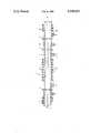
Features of the invention will become more apparent having regard to the following description in which reference is made to the accompanying drawing which schematically depicts a part of the apparatus employed.
Conventionally plasma deposition, plasma etching and plasma treatment are carried out using a continuous discharge. This invention is however, concerned with the alternative plasma process in which the plasma is intermittently powered, using a small mark to space ratio, so that high peak powers can be produced with a low mean power dissipation as described in United Kingdom Patent Specification No. 2105729A. By this means it has been found possible to produce, without recourse to significantly elevated substrate temperatures, extremely high dissocation of gases down to atomic species, thereby making it possible to deposit dense and composite films of novel materials such as nitrides, carbides, borides, and oxides upon plastics materials either individually or in combination. Such films may typically be produced using a peak power density of at least several kilowatts per liter using pulses of between 1 millisecond and 1 microsecond duration and a mark to space ratio providing a mean power density of not more than a few tens of watts per liter. The avoidance of significantly elevated substrate temperatures also permits special effects to be produced using the pulsed plasma for surface treatment of the plastics substrate, for instance by modifying the surface, degassing it, producing surface melting to remove defects such as cracks and pores, promoting cross linking, or implanting material from the plasma into the surface. A plused plasma in an argon hydrogen mixture can be used to produce cross linking of high density polyethylene to a depth of 3 microns, whereas with a continuous discharge the depth of cross linking is typically limited to about 0.5 microns.
One of the features of using pulsed plasma for surface treatment of a plastics coating on an optical fibre, whether or not this surface treatment involves implantation, is that it produces a surface that is harder and denser, and thus more suited to forming a reliable bond with a subsequently deposited moisture barrier layer. Usually, but not necessarily, it is convenient for that layer to be deposited by a method involving the use of a pulsed plasma.
In instances where the pulsed plasma is being used for surface smoothing of an optical fibre plastics coating it is generally preferred not to use pure argon for the plasma but a mixture of argon and hydrogen because the hydrogen is found to accelerate the processing by tending to break up bonds in the polymer chains, whereas the argon tends to promote cross linking of the plastics surface. Hydrogen species may for the same reason also be effective in the atmosphere when the surface treatment involves implantation, thus for instance an atmosphere of argon containing some silane may be used for implanting silicon into the plastics surface. Alternatively, a silicon chloride can replace silane as the source of silicon. This siliciding of the surface may follow an initial surface treatment with pulsed plasma that does not involve any implantation. Yet another way of achieving the desired siliciding is to impregnate the plastics with a liquid compound of silicon, such as a siloxane or an organo-silane, such as trimethyl silane, and to use the pulsed plasma in argon or in an argon hydrogen mixture to cause the liquid to react chemically with the plastics material.
Reverting attention to the use of pulsed plasma for surface modification involving deposition, a preferred material is a generally non-stoichoimetric composition of silicon and carbon or of silicon and nitrogen. Preferably this deposition is upon an optical fibre plastics cladding whose surface has already been treated or silicided by one of the pulse plasma techniques referred to previously. The atmosphere of the pulsed plasma is in this instance silane and acetylene for the `silicon carbide` deposition or silane and nitrogen for the `silicon nitride` deposition. Other materials that may be deposited in an analogous way include for example, alumina, titanium carbide and titanium nitride. Using a peak power density of only 12 kw per liter provides a deposition rate of about 0.1 microns per minute, and hence an adequate thickness of deposit in the region of 0.05 microns can be built up in about half a minute. By increasing the peak power density it should be possible to achieve a significant shortening of this deposition period. This is desirable because it makes it easier to perform the coating process on line with the drawing of the optical fibre from optical fibre preform.
Referring now to the accompanying drawing, an optical fibre 1 freshly drawn from preform and provided with a primary plastics coating on line with that drawing operation is drawn through a multisection processing chamber one of whose sections is indicated generally at 2. This section consists essentially of atubular glass chamber 3 having one or more exit ports 4 connected to vacuum pumps (not shown) and one or more inlet ports 5 connected to a gas supply (not shown). The chamber terminates inbaffle plates
Only one part of the pulsed plasma processing is carried out inchamber 3; other parts are carried out in other chambers 9 and 10 upstream and downstream ofchamber 3. In some circumstances the reactions in adjacent chambers may be such as to make direct connection possible, as illustrated by the connection betweenchambers 9 and 3; whereas in other circumstances a direct connection of this sort is undesirable. One reason may be that there is such a disparity in working pressure between the two chambers that there would be too much leakage of gas through the separating baffle from the higher pressure region into the lower pressure one. This problem may be overcome by an indirect connection such as that betweenchambers 3 and 10. In this instance leakage from one chamber to the other is prevented by the use of a pair ofbaffles intermediate section 12 which is evacuated by way of an outlet port 13.
In yet other circumstances leakage from one chamber into an adjacent chamber is no disadvantage, and indeed is welcomed because it helps achieve a smoother grading between the component parts of a moisture barrier layer.
A grading of the composition of the components of a moisture barrier layer is usually desirable because it generally provides better adhesion between the components than is presented by a relatively abrupt interface. Thus an initial pulsed plasma treatment to effect crosslinking of the plastics substrate material will in general produce a densification of the surface, making its properties closer to that of a subsequently applied layer deposited by pulsed plasma. Thus a better grading is achieved between the substrate and subsequently deposited material. It is then preferred gradually to change the deposition atmosphere encountered by the substrate so that the deposit gradually changes from an organic material to an inorganic material, such as aluminium or a carbide or nitride of silicon or titanium. Optionally the deposition may be continued further to grade back to a further organic layer which is hydrophobic. This may be for instance a fluorocarbon polymer layer. Apart from its reduced chemisorption of water, the presence of a fluorocarbon outer surface maybe advantageous in providing a low coefficient of friction for subsequent handling, for instance during cabling.
Claims (25)
1. A method of providing a coating with low water permeability upon a glass optical fibre, which method includes the step of using a pulsed plasma at reduced pressure and at a power level providing dissociation down to atomic species to modify the surface of a plastics coating with which the optical fibre has been provided.
2. A method as claimed in claim 1, wherein at least one aspect of the pulsed plasma induced modification takes the form of changing the structure of the surface region of material already present.
3. A method as claimed in claim 2, wherein the pulsed plasma induced modification also involves an etching away of some of the material already present.
4. A method as claimed in claim 1, wherein at least one aspect of the pulsed plasma induced modification takes the form of adding fresh material to the material already present.
5. A method as claimed in claim 1, wherein the pulsed plasma induced modification involves both the changing of the structure of the surface region of material already present and the adding of fresh material.
6. A method as claimed in claim 1, which method includes the step of using pulsed plasma in an atomosphere consisting of or including a mixture of argon and hydrogen to modify the surface of the plastics coating.
7. A method as claimed in claim 1, which method includes the step of using pulsed plasma to implant material into the surface of the plastics coating to chemically bond with the material of the plastics coating.
8. A method as claimed in claim 7, wherein said implanted material is silicon.
9. A method as claimed in claim 8, wherein the implantation of silicon is succeeded by the step of using pulsed plasma to coat the modified surface with an inorganic layer whose composition includes silicon.
10. A method as claimed in claim 9, wherein said inorganic layer is a generally non-stoichiometric composition of silicon and carbon.
11. A method as claimed in claim 9, wherein said inorganic layer is a generally non-stoichiometric composition of silicon and nitrogen.
12. A method as claimed in claim 1, which method includes the step of using pulsed plasma to cause liquid absorbed into the surface of the plastics coating to react chemically with the material of that coating.
13. A method as claimed in claim 12, wherein said chemical reaction is such as to cause silicon to be chemically bonded with the material of the plastics coating.
14. A method as claimed in claim 13, wherein the step of causing silicon to be chemically bonded with the material of plastics coating is succeeded by the step of using pulsed plasma to coat the modified surface with an inorganic layer whose composition includes silicon.
15. A method as claimed in claim 14, wherein the composition of the deposited layer is a generally non-stoichiometric composition of silicon and carbon.
16. A method as claimed in claim 14, wherein the composition of the deposited layer is a generally non-stoichiometric composition of silicon and nitrogen.
17. A method as claimed in claim 1, wherein pulsed plasma is used to modify the surface of the plastics coating by the promotion of crosslinking, wherein pulse plasma is used to deposit material matching the crosslinked material, whereby a grading is provided between the bulk material of the coating and the deposited material, and wherein the atmosphere to which the coating is exposed in the pulsed plasma is changed to grade the deposit from organic material to inorganic material.
18. A method as claimed in claim 17, wherein the inorganic material is a compound of silicon.
19. A method as claimed in claim 17, wherein the inorganic material is a compound of titanium.
20. A method as claimed in claim 17, wherein the inorganic material is a nitride.
21. A method as claimed in claim 17, wherein the inorganic material is a carbide.
22. A method as claimed in claim 17, wherein the inorganic material is alumina.
23. A method as claimed in claim 17, wherein the atmosphere is further changed to grade the deposit back from the inorganic layer to a further organic layer which further organic layer is a layer of hydrophobic material.
24. A method as claimed in claim 23, wherein the hydrophobic material is a fluorocarbon polymer.
25. A method as claimed in claim 1, wherein the coating is exposed to pulsed plasma in a cascaded arrangement of reaction chambers.
Applications Claiming Priority (2)
| Application Number | Priority Date | Filing Date | Title |
|---|---|---|---|
| GB8320773 | 1983-08-02 | ||
| GB08320773AGB2144343A (en) | 1983-08-02 | 1983-08-02 | Optical fibre manufacture |
Related Parent Applications (1)
| Application Number | Title | Priority Date | Filing Date |
|---|---|---|---|
| US06635812Continuation | 1984-07-30 |
Publications (1)
| Publication Number | Publication Date |
|---|---|
| US4568563Atrue US4568563A (en) | 1986-02-04 |
Family
ID=10546649
Family Applications (1)
| Application Number | Title | Priority Date | Filing Date |
|---|---|---|---|
| US06/747,389Expired - Fee RelatedUS4568563A (en) | 1983-08-02 | 1985-06-21 | Optical fibre manufacture |
Country Status (7)
| Country | Link |
|---|---|
| US (1) | US4568563A (en) |
| EP (1) | EP0135993A1 (en) |
| JP (1) | JPS6036356A (en) |
| KR (1) | KR850001511A (en) |
| AU (1) | AU3129784A (en) |
| ES (1) | ES8603087A1 (en) |
| GB (1) | GB2144343A (en) |
Cited By (54)
| Publication number | Priority date | Publication date | Assignee | Title |
|---|---|---|---|---|
| US4743662A (en)* | 1986-11-03 | 1988-05-10 | Dow Corning Corporation | Infusible preceramic polymers via plasma treatment |
| US4764394A (en)* | 1987-01-20 | 1988-08-16 | Wisconsin Alumni Research Foundation | Method and apparatus for plasma source ion implantation |
| US4842941A (en)* | 1987-04-06 | 1989-06-27 | General Electric Company | Method for forming abrasion-resistant polycarbonate articles, and articles of manufacture produced thereby |
| US4927704A (en)* | 1987-08-24 | 1990-05-22 | General Electric Company | Abrasion-resistant plastic articles and method for making them |
| US4964694A (en)* | 1988-07-26 | 1990-10-23 | Fujikura Ltd. | Optical fiber and apparatus for producing same |
| US4985112A (en)* | 1987-02-09 | 1991-01-15 | International Business Machines Corporation | Enhanced plasma etching |
| US4987005A (en)* | 1986-08-08 | 1991-01-22 | Semiconductor Energy Laboratory Co., Ltd. | Chemical vapor processing method for deposition or etching on a plurality of substrates |
| US5051308A (en)* | 1987-08-24 | 1991-09-24 | General Electric Company | Abrasion-resistant plastic articles |
| US5110409A (en)* | 1987-02-09 | 1992-05-05 | Ibm | Enhanced plasma etching |
| US5254372A (en)* | 1991-02-27 | 1993-10-19 | Nichols Technologies, Inc. | Method and apparatus for plasma treatment of a filament |
| US5389195A (en)* | 1991-03-07 | 1995-02-14 | Minnesota Mining And Manufacturing Company | Surface modification by accelerated plasma or ions |
| US5521351A (en)* | 1994-08-30 | 1996-05-28 | Wisconsin Alumni Research Foundation | Method and apparatus for plasma surface treatment of the interior of hollow forms |
| US5683757A (en)* | 1995-08-25 | 1997-11-04 | Iskanderova; Zelina A. | Surface modification of polymers and carbon-based materials by ion implantation and oxidative conversion |
| US5983828A (en)* | 1995-10-13 | 1999-11-16 | Mattson Technology, Inc. | Apparatus and method for pulsed plasma processing of a semiconductor substrate |
| US5985742A (en)* | 1997-05-12 | 1999-11-16 | Silicon Genesis Corporation | Controlled cleavage process and device for patterned films |
| US6027988A (en)* | 1997-05-28 | 2000-02-22 | The Regents Of The University Of California | Method of separating films from bulk substrates by plasma immersion ion implantation |
| US6030667A (en)* | 1996-02-27 | 2000-02-29 | Matsushita Electric Industrial Co., Ltd. | Apparatus and method for applying RF power apparatus and method for generating plasma and apparatus and method for processing with plasma |
| US6221740B1 (en) | 1999-08-10 | 2001-04-24 | Silicon Genesis Corporation | Substrate cleaving tool and method |
| US6263941B1 (en) | 1999-08-10 | 2001-07-24 | Silicon Genesis Corporation | Nozzle for cleaving substrates |
| US6284631B1 (en) | 1997-05-12 | 2001-09-04 | Silicon Genesis Corporation | Method and device for controlled cleaving process |
| US6291326B1 (en) | 1998-06-23 | 2001-09-18 | Silicon Genesis Corporation | Pre-semiconductor process implant and post-process film separation |
| US6291313B1 (en) | 1997-05-12 | 2001-09-18 | Silicon Genesis Corporation | Method and device for controlled cleaving process |
| US6355312B1 (en)* | 1998-10-16 | 2002-03-12 | Cottin Development, Inc. | Methods and apparatus for subjecting a rod-like or thread-like material to a plasma treatment |
| US6395641B2 (en) | 1995-10-13 | 2002-05-28 | Mattson Techonolgy, Inc. | Apparatus and method for pulsed plasma processing of a semiconductor substrate |
| US6500732B1 (en) | 1999-08-10 | 2002-12-31 | Silicon Genesis Corporation | Cleaving process to fabricate multilayered substrates using low implantation doses |
| US6536958B2 (en)* | 2000-12-20 | 2003-03-25 | Triquint Technology Holding Co. | Optical device package with hermetically bonded fibers |
| US6548382B1 (en) | 1997-07-18 | 2003-04-15 | Silicon Genesis Corporation | Gettering technique for wafers made using a controlled cleaving process |
| US20030124815A1 (en)* | 1999-08-10 | 2003-07-03 | Silicon Genesis Corporation | Cleaving process to fabricate multilayered substrates using low implantation doses |
| US20040067644A1 (en)* | 2002-10-04 | 2004-04-08 | Malik Igor J. | Non-contact etch annealing of strained layers |
| US6794301B2 (en) | 1995-10-13 | 2004-09-21 | Mattson Technology, Inc. | Pulsed plasma processing of semiconductor substrates |
| US20060252229A1 (en)* | 2003-06-24 | 2006-11-09 | Jean-Pierre Joly | Integrated circuit on high performance chip |
| USRE39484E1 (en) | 1991-09-18 | 2007-02-06 | Commissariat A L'energie Atomique | Process for the production of thin semiconductor material films |
| US20070281445A1 (en)* | 2003-10-28 | 2007-12-06 | Nguyet-Phuong Nguyen | Method for Self-Supported Transfer of a Fine Layer by Pulsation after Implantation or Co-Implantation |
| US20080038901A1 (en)* | 1997-05-12 | 2008-02-14 | Silicon Genesis Corporation | Controlled Process and Resulting Device |
| US20080153220A1 (en)* | 2003-11-18 | 2008-06-26 | Silicon Genesis Corporation | Method for fabricating semiconductor devices using strained silicon bearing material |
| US20080179547A1 (en)* | 2006-09-08 | 2008-07-31 | Silicon Genesis Corporation | Method and structure for fabricating solar cells using a thick layer transfer process |
| US20090120568A1 (en)* | 2005-08-16 | 2009-05-14 | Chrystel Deguet | Method of transferring a thin film onto a support |
| US20090130392A1 (en)* | 1996-05-15 | 2009-05-21 | Commissariat A L'energie Atomique (Cea) | Method of producing a thin layer of semiconductor material |
| US20090156016A1 (en)* | 2007-12-17 | 2009-06-18 | Lea Di Cioccio | Method for transfer of a thin layer |
| US20100025228A1 (en)* | 2006-12-19 | 2010-02-04 | Tauzin Aurelie | Method for Preparing Thin GaN Layers by Implantation and Recycling of a Starting Substrate |
| US20100044595A1 (en)* | 2008-08-25 | 2010-02-25 | Silicon Genesis Corporation | Race track configuration and method for wafering silicon solar substrates |
| US20100167499A1 (en)* | 2002-12-09 | 2010-07-01 | Commissariat A L'energie Atomique | Method for making a stressed structure designed to be dissociated |
| US20100216294A1 (en)* | 2007-10-12 | 2010-08-26 | Marc Rabarot | Method of fabricating a microelectronic structure involving molecular bonding |
| US20100317140A1 (en)* | 2009-05-13 | 2010-12-16 | Silicon Genesis Corporation | Techniques for forming thin films by implantation with reduced channeling |
| US20100323497A1 (en)* | 2009-06-18 | 2010-12-23 | Franck Fournel | Method of transferring a thin layer onto a target substrate having a coefficient of thermal expansion different from that of the thin layer |
| US7883994B2 (en) | 1997-12-30 | 2011-02-08 | Commissariat A L'energie Atomique | Process for the transfer of a thin film |
| US7902038B2 (en) | 2001-04-13 | 2011-03-08 | Commissariat A L'energie Atomique | Detachable substrate with controlled mechanical strength and method of producing same |
| US20120006468A1 (en)* | 2010-07-07 | 2012-01-12 | Schlumberger Technology Corporation | Inline plasma treatment of an optical fiber cable structure |
| US8193069B2 (en) | 2003-07-21 | 2012-06-05 | Commissariat A L'energie Atomique | Stacked structure and production method thereof |
| US8293619B2 (en) | 2008-08-28 | 2012-10-23 | Silicon Genesis Corporation | Layer transfer of films utilizing controlled propagation |
| US20120321776A1 (en)* | 2011-06-17 | 2012-12-20 | Robert Vetrecin | Process for in situ plasma polymerization of silicone coatings for surgical needles |
| US8664084B2 (en) | 2005-09-28 | 2014-03-04 | Commissariat A L'energie Atomique | Method for making a thin-film element |
| US8993410B2 (en) | 2006-09-08 | 2015-03-31 | Silicon Genesis Corporation | Substrate cleaving under controlled stress conditions |
| US9362439B2 (en) | 2008-05-07 | 2016-06-07 | Silicon Genesis Corporation | Layer transfer of films utilizing controlled shear region |
Families Citing this family (8)
| Publication number | Priority date | Publication date | Assignee | Title |
|---|---|---|---|---|
| US4750806A (en)* | 1985-06-17 | 1988-06-14 | Alcatel Usa Corporation | Glass fibers and capillaries with high temperature resistant coatings |
| GB2150858B (en)* | 1983-12-06 | 1986-11-26 | Standard Telephones Cables Ltd | Optical fibres |
| GB2155024A (en)* | 1984-03-03 | 1985-09-18 | Standard Telephones Cables Ltd | Surface treatment of plastics materials |
| CA1278193C (en)* | 1985-07-05 | 1990-12-27 | Brian G. Bagley | Method for preparation of silicate glasses of controlled index ofrefraction and optical device including same |
| DE3926592A1 (en)* | 1989-08-11 | 1991-02-14 | Rheydt Kabelwerk Ag | OPTICAL FIBER |
| US5141595A (en)* | 1990-03-05 | 1992-08-25 | Northrop Corporation | Method and apparatus for carbon coating and boron-doped carbon coating |
| US5109442A (en)* | 1990-03-28 | 1992-04-28 | Fiberchem Inc. | Waterproof optical fiber chemical sensor and method of making same |
| FR2753540B1 (en)* | 1996-09-13 | 1998-11-13 | Alcatel Cable | OPTICAL CONDUCTOR AND MANUFACTURING METHOD THEREOF |
Citations (13)
| Publication number | Priority date | Publication date | Assignee | Title |
|---|---|---|---|---|
| US313029A (en)* | 1885-02-24 | Method of making ornamental and other designs in relief | ||
| US3288638A (en)* | 1962-10-09 | 1966-11-29 | Martin Marietta Corp | Method and apparatus for the treatment of plastic materials |
| US3471316A (en)* | 1965-06-14 | 1969-10-07 | Continental Can Co | Method of forming a flexible organic layer on metal by a pulsed electrical abnormal glow discharge |
| US3677799A (en)* | 1970-11-10 | 1972-07-18 | Celanese Corp | Vapor phase boron deposition by pulse discharge |
| USB313029I5 (en) | 1970-10-13 | 1975-01-28 | ||
| DE2444926A1 (en)* | 1974-09-20 | 1976-04-08 | Felten & Guilleaume Dielektra | Continuous insulation of wires - by applying polymer layer by condensn polymerisation from gas phase using glow discharge |
| US4091166A (en)* | 1977-06-17 | 1978-05-23 | The United States Of America As Represented By The Administrator Of The National Aeronautics And Space Administration | Boron trifluoride coatings for thermoplastic materials and method of applying same in glow discharge |
| US4227907A (en)* | 1979-10-22 | 1980-10-14 | The United States Of America As Represented By The Secretary Of The Army | Laser photochemical synthesis coating of optical fiber |
| GB2105371A (en)* | 1981-08-18 | 1983-03-23 | Secr Defence | Carbon deposited on fibre by glow discharge method |
| GB2105729A (en)* | 1981-09-15 | 1983-03-30 | Itt Ind Ltd | Surface processing of a substrate material |
| US4396641A (en)* | 1980-09-08 | 1983-08-02 | Shin-Etsu Chemical Co., Ltd. | Method for improving surface properties of shaped articles of synthetic resins |
| US4402993A (en)* | 1981-03-20 | 1983-09-06 | Gulf & Western Manufacturing Company | Process for coating optical fibers |
| US4410567A (en)* | 1979-02-01 | 1983-10-18 | Post Office | Optical fibres and coatings therefor |
- 1983
- 1983-08-02GBGB08320773Apatent/GB2144343A/ennot_activeWithdrawn
- 1984
- 1984-07-10EPEP84304691Apatent/EP0135993A1/ennot_activeWithdrawn
- 1984-07-24JPJP59153924Apatent/JPS6036356A/enactivePending
- 1984-07-30AUAU31297/84Apatent/AU3129784A/ennot_activeAbandoned
- 1984-08-01KRKR1019840004592Apatent/KR850001511A/ennot_activeWithdrawn
- 1984-08-02ESES534837Apatent/ES8603087A1/ennot_activeExpired
- 1985
- 1985-06-21USUS06/747,389patent/US4568563A/ennot_activeExpired - Fee Related
Patent Citations (13)
| Publication number | Priority date | Publication date | Assignee | Title |
|---|---|---|---|---|
| US313029A (en)* | 1885-02-24 | Method of making ornamental and other designs in relief | ||
| US3288638A (en)* | 1962-10-09 | 1966-11-29 | Martin Marietta Corp | Method and apparatus for the treatment of plastic materials |
| US3471316A (en)* | 1965-06-14 | 1969-10-07 | Continental Can Co | Method of forming a flexible organic layer on metal by a pulsed electrical abnormal glow discharge |
| USB313029I5 (en) | 1970-10-13 | 1975-01-28 | ||
| US3677799A (en)* | 1970-11-10 | 1972-07-18 | Celanese Corp | Vapor phase boron deposition by pulse discharge |
| DE2444926A1 (en)* | 1974-09-20 | 1976-04-08 | Felten & Guilleaume Dielektra | Continuous insulation of wires - by applying polymer layer by condensn polymerisation from gas phase using glow discharge |
| US4091166A (en)* | 1977-06-17 | 1978-05-23 | The United States Of America As Represented By The Administrator Of The National Aeronautics And Space Administration | Boron trifluoride coatings for thermoplastic materials and method of applying same in glow discharge |
| US4410567A (en)* | 1979-02-01 | 1983-10-18 | Post Office | Optical fibres and coatings therefor |
| US4227907A (en)* | 1979-10-22 | 1980-10-14 | The United States Of America As Represented By The Secretary Of The Army | Laser photochemical synthesis coating of optical fiber |
| US4396641A (en)* | 1980-09-08 | 1983-08-02 | Shin-Etsu Chemical Co., Ltd. | Method for improving surface properties of shaped articles of synthetic resins |
| US4402993A (en)* | 1981-03-20 | 1983-09-06 | Gulf & Western Manufacturing Company | Process for coating optical fibers |
| GB2105371A (en)* | 1981-08-18 | 1983-03-23 | Secr Defence | Carbon deposited on fibre by glow discharge method |
| GB2105729A (en)* | 1981-09-15 | 1983-03-30 | Itt Ind Ltd | Surface processing of a substrate material |
Non-Patent Citations (2)
| Title |
|---|
| Chemical Abstracts, vol. 90, No. 16, Apr. 1979, p. 24, No. 122383f, Stenyushin et al.* |
| Chemical Abstracts, vol. 95, No. 8, Aug., 1981, p. 286, No. 66591m.* |
Cited By (108)
| Publication number | Priority date | Publication date | Assignee | Title |
|---|---|---|---|---|
| US4987005A (en)* | 1986-08-08 | 1991-01-22 | Semiconductor Energy Laboratory Co., Ltd. | Chemical vapor processing method for deposition or etching on a plurality of substrates |
| US4743662A (en)* | 1986-11-03 | 1988-05-10 | Dow Corning Corporation | Infusible preceramic polymers via plasma treatment |
| US4764394A (en)* | 1987-01-20 | 1988-08-16 | Wisconsin Alumni Research Foundation | Method and apparatus for plasma source ion implantation |
| US4985112A (en)* | 1987-02-09 | 1991-01-15 | International Business Machines Corporation | Enhanced plasma etching |
| US5110409A (en)* | 1987-02-09 | 1992-05-05 | Ibm | Enhanced plasma etching |
| US4842941A (en)* | 1987-04-06 | 1989-06-27 | General Electric Company | Method for forming abrasion-resistant polycarbonate articles, and articles of manufacture produced thereby |
| US4927704A (en)* | 1987-08-24 | 1990-05-22 | General Electric Company | Abrasion-resistant plastic articles and method for making them |
| US5051308A (en)* | 1987-08-24 | 1991-09-24 | General Electric Company | Abrasion-resistant plastic articles |
| US4964694A (en)* | 1988-07-26 | 1990-10-23 | Fujikura Ltd. | Optical fiber and apparatus for producing same |
| US5254372A (en)* | 1991-02-27 | 1993-10-19 | Nichols Technologies, Inc. | Method and apparatus for plasma treatment of a filament |
| US5389195A (en)* | 1991-03-07 | 1995-02-14 | Minnesota Mining And Manufacturing Company | Surface modification by accelerated plasma or ions |
| USRE39484E1 (en) | 1991-09-18 | 2007-02-06 | Commissariat A L'energie Atomique | Process for the production of thin semiconductor material films |
| US5521351A (en)* | 1994-08-30 | 1996-05-28 | Wisconsin Alumni Research Foundation | Method and apparatus for plasma surface treatment of the interior of hollow forms |
| US5683757A (en)* | 1995-08-25 | 1997-11-04 | Iskanderova; Zelina A. | Surface modification of polymers and carbon-based materials by ion implantation and oxidative conversion |
| US5983828A (en)* | 1995-10-13 | 1999-11-16 | Mattson Technology, Inc. | Apparatus and method for pulsed plasma processing of a semiconductor substrate |
| US6395641B2 (en) | 1995-10-13 | 2002-05-28 | Mattson Techonolgy, Inc. | Apparatus and method for pulsed plasma processing of a semiconductor substrate |
| US6794301B2 (en) | 1995-10-13 | 2004-09-21 | Mattson Technology, Inc. | Pulsed plasma processing of semiconductor substrates |
| US6030667A (en)* | 1996-02-27 | 2000-02-29 | Matsushita Electric Industrial Co., Ltd. | Apparatus and method for applying RF power apparatus and method for generating plasma and apparatus and method for processing with plasma |
| US8101503B2 (en) | 1996-05-15 | 2012-01-24 | Commissariat A L'energie Atomique | Method of producing a thin layer of semiconductor material |
| US20090130392A1 (en)* | 1996-05-15 | 2009-05-21 | Commissariat A L'energie Atomique (Cea) | Method of producing a thin layer of semiconductor material |
| US20050186758A1 (en)* | 1997-05-12 | 2005-08-25 | Silicon Genesis Corporation | Controlled cleaving process |
| US5985742A (en)* | 1997-05-12 | 1999-11-16 | Silicon Genesis Corporation | Controlled cleavage process and device for patterned films |
| US6155909A (en)* | 1997-05-12 | 2000-12-05 | Silicon Genesis Corporation | Controlled cleavage system using pressurized fluid |
| US6159825A (en)* | 1997-05-12 | 2000-12-12 | Silicon Genesis Corporation | Controlled cleavage thin film separation process using a reusable substrate |
| US6159824A (en)* | 1997-05-12 | 2000-12-12 | Silicon Genesis Corporation | Silicon-on-silicon wafer bonding process using a thin film blister-separation method |
| US6162705A (en)* | 1997-05-12 | 2000-12-19 | Silicon Genesis Corporation | Controlled cleavage process and resulting device using beta annealing |
| US6187110B1 (en) | 1997-05-12 | 2001-02-13 | Silicon Genesis Corporation | Device for patterned films |
| US20080286945A1 (en)* | 1997-05-12 | 2008-11-20 | Silicon Genesis Corporation | Controlled process and resulting device |
| US6245161B1 (en) | 1997-05-12 | 2001-06-12 | Silicon Genesis Corporation | Economical silicon-on-silicon hybrid wafer assembly |
| US7371660B2 (en) | 1997-05-12 | 2008-05-13 | Silicon Genesis Corporation | Controlled cleaving process |
| US6284631B1 (en) | 1997-05-12 | 2001-09-04 | Silicon Genesis Corporation | Method and device for controlled cleaving process |
| US7348258B2 (en) | 1997-05-12 | 2008-03-25 | Silicon Genesis Corporation | Method and device for controlled cleaving process |
| US6291313B1 (en) | 1997-05-12 | 2001-09-18 | Silicon Genesis Corporation | Method and device for controlled cleaving process |
| US6294814B1 (en) | 1997-05-12 | 2001-09-25 | Silicon Genesis Corporation | Cleaved silicon thin film with rough surface |
| US20080038901A1 (en)* | 1997-05-12 | 2008-02-14 | Silicon Genesis Corporation | Controlled Process and Resulting Device |
| US6391740B1 (en) | 1997-05-12 | 2002-05-21 | Silicon Genesis Corporation | Generic layer transfer methodology by controlled cleavage process |
| US6048411A (en)* | 1997-05-12 | 2000-04-11 | Silicon Genesis Corporation | Silicon-on-silicon hybrid wafer assembly |
| US6458672B1 (en) | 1997-05-12 | 2002-10-01 | Silicon Genesis Corporation | Controlled cleavage process and resulting device using beta annealing |
| US6486041B2 (en) | 1997-05-12 | 2002-11-26 | Silicon Genesis Corporation | Method and device for controlled cleaving process |
| US7759217B2 (en) | 1997-05-12 | 2010-07-20 | Silicon Genesis Corporation | Controlled process and resulting device |
| US6511899B1 (en) | 1997-05-12 | 2003-01-28 | Silicon Genesis Corporation | Controlled cleavage process using pressurized fluid |
| US6146979A (en)* | 1997-05-12 | 2000-11-14 | Silicon Genesis Corporation | Pressurized microbubble thin film separation process using a reusable substrate |
| US6528391B1 (en) | 1997-05-12 | 2003-03-04 | Silicon Genesis, Corporation | Controlled cleavage process and device for patterned films |
| US5994207A (en)* | 1997-05-12 | 1999-11-30 | Silicon Genesis Corporation | Controlled cleavage process using pressurized fluid |
| US20070123013A1 (en)* | 1997-05-12 | 2007-05-31 | Silicon Genesis Corporation | Controlled process and resulting device |
| US6558802B1 (en) | 1997-05-12 | 2003-05-06 | Silicon Genesis Corporation | Silicon-on-silicon hybrid wafer assembly |
| US20030113983A1 (en)* | 1997-05-12 | 2003-06-19 | Silicon Genesis Corporation | Method and device for controlled cleaving process |
| US6010579A (en)* | 1997-05-12 | 2000-01-04 | Silicon Genesis Corporation | Reusable substrate for thin film separation |
| US6632724B2 (en) | 1997-05-12 | 2003-10-14 | Silicon Genesis Corporation | Controlled cleaving process |
| US7846818B2 (en) | 1997-05-12 | 2010-12-07 | Silicon Genesis Corporation | Controlled process and resulting device |
| US7160790B2 (en) | 1997-05-12 | 2007-01-09 | Silicon Genesis Corporation | Controlled cleaving process |
| US6790747B2 (en) | 1997-05-12 | 2004-09-14 | Silicon Genesis Corporation | Method and device for controlled cleaving process |
| US7776717B2 (en) | 1997-05-12 | 2010-08-17 | Silicon Genesis Corporation | Controlled process and resulting device |
| US20050070071A1 (en)* | 1997-05-12 | 2005-03-31 | Silicon Genesis Corporation | Method and device for controlled cleaving process |
| US7410887B2 (en) | 1997-05-12 | 2008-08-12 | Silicon Genesis Corporation | Controlled process and resulting device |
| US6013563A (en)* | 1997-05-12 | 2000-01-11 | Silicon Genesis Corporation | Controlled cleaning process |
| US6027988A (en)* | 1997-05-28 | 2000-02-22 | The Regents Of The University Of California | Method of separating films from bulk substrates by plasma immersion ion implantation |
| US6890838B2 (en) | 1997-07-18 | 2005-05-10 | Silicon Genesis Corporation | Gettering technique for wafers made using a controlled cleaving process |
| US20040097055A1 (en)* | 1997-07-18 | 2004-05-20 | Silicon Genesis Corporation | Gettering technique for wafers made using a controlled cleaving process |
| US6548382B1 (en) | 1997-07-18 | 2003-04-15 | Silicon Genesis Corporation | Gettering technique for wafers made using a controlled cleaving process |
| US8609514B2 (en) | 1997-12-10 | 2013-12-17 | Commissariat A L'energie Atomique | Process for the transfer of a thin film comprising an inclusion creation step |
| US7883994B2 (en) | 1997-12-30 | 2011-02-08 | Commissariat A L'energie Atomique | Process for the transfer of a thin film |
| US20110092051A1 (en)* | 1997-12-30 | 2011-04-21 | Commissariat A L'energie Atomique | Process for the transfer of a thin film comprising an inclusion creation step |
| US8470712B2 (en) | 1997-12-30 | 2013-06-25 | Commissariat A L'energie Atomique | Process for the transfer of a thin film comprising an inclusion creation step |
| US6291326B1 (en) | 1998-06-23 | 2001-09-18 | Silicon Genesis Corporation | Pre-semiconductor process implant and post-process film separation |
| US6355312B1 (en)* | 1998-10-16 | 2002-03-12 | Cottin Development, Inc. | Methods and apparatus for subjecting a rod-like or thread-like material to a plasma treatment |
| US6513564B2 (en) | 1999-08-10 | 2003-02-04 | Silicon Genesis Corporation | Nozzle for cleaving substrates |
| US7056808B2 (en) | 1999-08-10 | 2006-06-06 | Silicon Genesis Corporation | Cleaving process to fabricate multilayered substrates using low implantation doses |
| US6221740B1 (en) | 1999-08-10 | 2001-04-24 | Silicon Genesis Corporation | Substrate cleaving tool and method |
| US6263941B1 (en) | 1999-08-10 | 2001-07-24 | Silicon Genesis Corporation | Nozzle for cleaving substrates |
| US6500732B1 (en) | 1999-08-10 | 2002-12-31 | Silicon Genesis Corporation | Cleaving process to fabricate multilayered substrates using low implantation doses |
| US20030124815A1 (en)* | 1999-08-10 | 2003-07-03 | Silicon Genesis Corporation | Cleaving process to fabricate multilayered substrates using low implantation doses |
| US6536958B2 (en)* | 2000-12-20 | 2003-03-25 | Triquint Technology Holding Co. | Optical device package with hermetically bonded fibers |
| US7902038B2 (en) | 2001-04-13 | 2011-03-08 | Commissariat A L'energie Atomique | Detachable substrate with controlled mechanical strength and method of producing same |
| US8187377B2 (en) | 2002-10-04 | 2012-05-29 | Silicon Genesis Corporation | Non-contact etch annealing of strained layers |
| US20040067644A1 (en)* | 2002-10-04 | 2004-04-08 | Malik Igor J. | Non-contact etch annealing of strained layers |
| US20100167499A1 (en)* | 2002-12-09 | 2010-07-01 | Commissariat A L'energie Atomique | Method for making a stressed structure designed to be dissociated |
| US8389379B2 (en) | 2002-12-09 | 2013-03-05 | Commissariat A L'energie Atomique | Method for making a stressed structure designed to be dissociated |
| US20060252229A1 (en)* | 2003-06-24 | 2006-11-09 | Jean-Pierre Joly | Integrated circuit on high performance chip |
| US8048766B2 (en) | 2003-06-24 | 2011-11-01 | Commissariat A L'energie Atomique | Integrated circuit on high performance chip |
| US8193069B2 (en) | 2003-07-21 | 2012-06-05 | Commissariat A L'energie Atomique | Stacked structure and production method thereof |
| US8309431B2 (en) | 2003-10-28 | 2012-11-13 | Commissariat A L'energie Atomique | Method for self-supported transfer of a fine layer by pulsation after implantation or co-implantation |
| US20070281445A1 (en)* | 2003-10-28 | 2007-12-06 | Nguyet-Phuong Nguyen | Method for Self-Supported Transfer of a Fine Layer by Pulsation after Implantation or Co-Implantation |
| US20080153220A1 (en)* | 2003-11-18 | 2008-06-26 | Silicon Genesis Corporation | Method for fabricating semiconductor devices using strained silicon bearing material |
| US8142593B2 (en) | 2005-08-16 | 2012-03-27 | Commissariat A L'energie Atomique | Method of transferring a thin film onto a support |
| US20090120568A1 (en)* | 2005-08-16 | 2009-05-14 | Chrystel Deguet | Method of transferring a thin film onto a support |
| US8664084B2 (en) | 2005-09-28 | 2014-03-04 | Commissariat A L'energie Atomique | Method for making a thin-film element |
| US9356181B2 (en) | 2006-09-08 | 2016-05-31 | Silicon Genesis Corporation | Substrate cleaving under controlled stress conditions |
| US9640711B2 (en) | 2006-09-08 | 2017-05-02 | Silicon Genesis Corporation | Substrate cleaving under controlled stress conditions |
| US8993410B2 (en) | 2006-09-08 | 2015-03-31 | Silicon Genesis Corporation | Substrate cleaving under controlled stress conditions |
| US7811900B2 (en) | 2006-09-08 | 2010-10-12 | Silicon Genesis Corporation | Method and structure for fabricating solar cells using a thick layer transfer process |
| US20080179547A1 (en)* | 2006-09-08 | 2008-07-31 | Silicon Genesis Corporation | Method and structure for fabricating solar cells using a thick layer transfer process |
| US8778775B2 (en) | 2006-12-19 | 2014-07-15 | Commissariat A L'energie Atomique | Method for preparing thin GaN layers by implantation and recycling of a starting substrate |
| US20100025228A1 (en)* | 2006-12-19 | 2010-02-04 | Tauzin Aurelie | Method for Preparing Thin GaN Layers by Implantation and Recycling of a Starting Substrate |
| US20100216294A1 (en)* | 2007-10-12 | 2010-08-26 | Marc Rabarot | Method of fabricating a microelectronic structure involving molecular bonding |
| US20090156016A1 (en)* | 2007-12-17 | 2009-06-18 | Lea Di Cioccio | Method for transfer of a thin layer |
| US7960248B2 (en) | 2007-12-17 | 2011-06-14 | Commissariat A L'energie Atomique | Method for transfer of a thin layer |
| US11444221B2 (en) | 2008-05-07 | 2022-09-13 | Silicon Genesis Corporation | Layer transfer of films utilizing controlled shear region |
| US9362439B2 (en) | 2008-05-07 | 2016-06-07 | Silicon Genesis Corporation | Layer transfer of films utilizing controlled shear region |
| US8330126B2 (en) | 2008-08-25 | 2012-12-11 | Silicon Genesis Corporation | Race track configuration and method for wafering silicon solar substrates |
| US20100044595A1 (en)* | 2008-08-25 | 2010-02-25 | Silicon Genesis Corporation | Race track configuration and method for wafering silicon solar substrates |
| US8293619B2 (en) | 2008-08-28 | 2012-10-23 | Silicon Genesis Corporation | Layer transfer of films utilizing controlled propagation |
| US8329557B2 (en) | 2009-05-13 | 2012-12-11 | Silicon Genesis Corporation | Techniques for forming thin films by implantation with reduced channeling |
| US20100317140A1 (en)* | 2009-05-13 | 2010-12-16 | Silicon Genesis Corporation | Techniques for forming thin films by implantation with reduced channeling |
| US8252663B2 (en) | 2009-06-18 | 2012-08-28 | Commissariat A L'energie Atomique Et Aux Energies Alternatives | Method of transferring a thin layer onto a target substrate having a coefficient of thermal expansion different from that of the thin layer |
| US20100323497A1 (en)* | 2009-06-18 | 2010-12-23 | Franck Fournel | Method of transferring a thin layer onto a target substrate having a coefficient of thermal expansion different from that of the thin layer |
| US20120006468A1 (en)* | 2010-07-07 | 2012-01-12 | Schlumberger Technology Corporation | Inline plasma treatment of an optical fiber cable structure |
| US20120321776A1 (en)* | 2011-06-17 | 2012-12-20 | Robert Vetrecin | Process for in situ plasma polymerization of silicone coatings for surgical needles |
Also Published As
| Publication number | Publication date |
|---|---|
| JPS6036356A (en) | 1985-02-25 |
| GB8320773D0 (en) | 1983-09-01 |
| KR850001511A (en) | 1985-03-30 |
| GB2144343A (en) | 1985-03-06 |
| ES534837A0 (en) | 1985-11-01 |
| EP0135993A1 (en) | 1985-04-03 |
| ES8603087A1 (en) | 1985-11-01 |
| AU3129784A (en) | 1985-02-07 |
Similar Documents
| Publication | Publication Date | Title |
|---|---|---|
| US4568563A (en) | Optical fibre manufacture | |
| EP1472387B1 (en) | Corona-generated chemical vapor deposition on a substrate | |
| US4824690A (en) | Pulsed plasma process for treating a substrate | |
| EP0308143B1 (en) | Hermetically sealed optical fibers | |
| DE69530758T2 (en) | ION BEAM PROCESS FOR PRODUCING HIGH-ABRASION-RESISTANT COATINGS | |
| DE69605280T2 (en) | METHOD FOR APPLYING DIAMOND-LIKE CARBON FILMS | |
| US5000541A (en) | Hermetically sealed optical fibers | |
| US4388344A (en) | Method of repairing surface defects in coated laser mirrors | |
| EP0515186B1 (en) | Process for preparing densified porous billets | |
| JP2003526010A (en) | Diamond-like glass thin film | |
| JP2005504330A (en) | Optical article and optoelectronic article | |
| US7496255B2 (en) | Radiation-transmissive films on glass articles | |
| EP0154482B1 (en) | Coating process | |
| US20030049468A1 (en) | Cascade arc plasma and abrasion resistant coatings made therefrom | |
| US5498760A (en) | Process and system for protecting an oxidizable material against oxidation | |
| CN1113826C (en) | Method for depositing coating layer on optical fibre while it is being drawn and device for its implementation | |
| KR20010079710A (en) | Process for the production of improved boron coatings onto graphite and article obtained in this process | |
| JP7149778B2 (en) | Superhydrophilic coating and method of forming the same | |
| RU2065508C1 (en) | Method for application of carbon protective coating | |
| GB2354188A (en) | Plasma treatment of substrate for adhesive or coating | |
| Moore et al. | Oxidation Protection of Carbon‐Carbon Composites by (B+ Si) N Coatings | |
| HK1072279B (en) | Corona-generated chemical vapor deposition on a substrate | |
| CN1561314A (en) | Method and device for depositing a glass layer on the outer surface of a rod-shaped preform | |
| McGinn et al. | Variations in nanostructure and composition for controlling the interfacial properties of metal matrix composites and ceramic matrix composites | |
| Wach et al. | Development of silicon carbide coating on Al2O3 ceramics from precursor polymers by radiation curing |
Legal Events
| Date | Code | Title | Description |
|---|---|---|---|
| REMI | Maintenance fee reminder mailed | ||
| LAPS | Lapse for failure to pay maintenance fees | ||
| STCH | Information on status: patent discontinuation | Free format text:PATENT EXPIRED DUE TO NONPAYMENT OF MAINTENANCE FEES UNDER 37 CFR 1.362 | |
| FP | Lapsed due to failure to pay maintenance fee | Effective date:19900204 |