US4539061A - Process for the production of built-up films by the stepwise adsorption of individual monolayers - Google Patents
Process for the production of built-up films by the stepwise adsorption of individual monolayersDownload PDFInfo
- Publication number
- US4539061A US4539061AUS06/530,102US53010283AUS4539061AUS 4539061 AUS4539061 AUS 4539061AUS 53010283 AUS53010283 AUS 53010283AUS 4539061 AUS4539061 AUS 4539061A
- Authority
- US
- United States
- Prior art keywords
- groups
- polar
- monolayer
- process according
- conversion
- Prior art date
- Legal status (The legal status is an assumption and is not a legal conclusion. Google has not performed a legal analysis and makes no representation as to the accuracy of the status listed.)
- Expired - Fee Related
Links
Images

Classifications
- H—ELECTRICITY
- H01—ELECTRIC ELEMENTS
- H01L—SEMICONDUCTOR DEVICES NOT COVERED BY CLASS H10
- H01L21/00—Processes or apparatus adapted for the manufacture or treatment of semiconductor or solid state devices or of parts thereof
- H01L21/02—Manufacture or treatment of semiconductor devices or of parts thereof
- H01L21/02104—Forming layers
- H01L21/02107—Forming insulating materials on a substrate
- H01L21/02109—Forming insulating materials on a substrate characterised by the type of layer, e.g. type of material, porous/non-porous, pre-cursors, mixtures or laminates
- H01L21/02112—Forming insulating materials on a substrate characterised by the type of layer, e.g. type of material, porous/non-porous, pre-cursors, mixtures or laminates characterised by the material of the layer
- H01L21/02123—Forming insulating materials on a substrate characterised by the type of layer, e.g. type of material, porous/non-porous, pre-cursors, mixtures or laminates characterised by the material of the layer the material containing silicon
- H01L21/02126—Forming insulating materials on a substrate characterised by the type of layer, e.g. type of material, porous/non-porous, pre-cursors, mixtures or laminates characterised by the material of the layer the material containing silicon the material containing Si, O, and at least one of H, N, C, F, or other non-metal elements, e.g. SiOC, SiOC:H or SiONC
- B—PERFORMING OPERATIONS; TRANSPORTING
- B05—SPRAYING OR ATOMISING IN GENERAL; APPLYING FLUENT MATERIALS TO SURFACES, IN GENERAL
- B05D—PROCESSES FOR APPLYING FLUENT MATERIALS TO SURFACES, IN GENERAL
- B05D1/00—Processes for applying liquids or other fluent materials
- B05D1/18—Processes for applying liquids or other fluent materials performed by dipping
- B05D1/185—Processes for applying liquids or other fluent materials performed by dipping applying monomolecular layers
- B—PERFORMING OPERATIONS; TRANSPORTING
- B05—SPRAYING OR ATOMISING IN GENERAL; APPLYING FLUENT MATERIALS TO SURFACES, IN GENERAL
- B05D—PROCESSES FOR APPLYING FLUENT MATERIALS TO SURFACES, IN GENERAL
- B05D1/00—Processes for applying liquids or other fluent materials
- B05D1/18—Processes for applying liquids or other fluent materials performed by dipping
- B05D1/20—Processes for applying liquids or other fluent materials performed by dipping substances to be applied floating on a fluid
- B05D1/202—Langmuir Blodgett films (LB films)
- B05D1/208—After-treatment of monomolecular films
- B—PERFORMING OPERATIONS; TRANSPORTING
- B82—NANOTECHNOLOGY
- B82Y—SPECIFIC USES OR APPLICATIONS OF NANOSTRUCTURES; MEASUREMENT OR ANALYSIS OF NANOSTRUCTURES; MANUFACTURE OR TREATMENT OF NANOSTRUCTURES
- B82Y30/00—Nanotechnology for materials or surface science, e.g. nanocomposites
- B—PERFORMING OPERATIONS; TRANSPORTING
- B82—NANOTECHNOLOGY
- B82Y—SPECIFIC USES OR APPLICATIONS OF NANOSTRUCTURES; MEASUREMENT OR ANALYSIS OF NANOSTRUCTURES; MANUFACTURE OR TREATMENT OF NANOSTRUCTURES
- B82Y40/00—Manufacture or treatment of nanostructures
- C—CHEMISTRY; METALLURGY
- C09—DYES; PAINTS; POLISHES; NATURAL RESINS; ADHESIVES; COMPOSITIONS NOT OTHERWISE PROVIDED FOR; APPLICATIONS OF MATERIALS NOT OTHERWISE PROVIDED FOR
- C09D—COATING COMPOSITIONS, e.g. PAINTS, VARNISHES OR LACQUERS; FILLING PASTES; CHEMICAL PAINT OR INK REMOVERS; INKS; CORRECTING FLUIDS; WOODSTAINS; PASTES OR SOLIDS FOR COLOURING OR PRINTING; USE OF MATERIALS THEREFOR
- C09D4/00—Coating compositions, e.g. paints, varnishes or lacquers, based on organic non-macromolecular compounds having at least one polymerisable carbon-to-carbon unsaturated bond ; Coating compositions, based on monomers of macromolecular compounds of groups C09D183/00 - C09D183/16
- G—PHYSICS
- G03—PHOTOGRAPHY; CINEMATOGRAPHY; ANALOGOUS TECHNIQUES USING WAVES OTHER THAN OPTICAL WAVES; ELECTROGRAPHY; HOLOGRAPHY
- G03F—PHOTOMECHANICAL PRODUCTION OF TEXTURED OR PATTERNED SURFACES, e.g. FOR PRINTING, FOR PROCESSING OF SEMICONDUCTOR DEVICES; MATERIALS THEREFOR; ORIGINALS THEREFOR; APPARATUS SPECIALLY ADAPTED THEREFOR
- G03F7/00—Photomechanical, e.g. photolithographic, production of textured or patterned surfaces, e.g. printing surfaces; Materials therefor, e.g. comprising photoresists; Apparatus specially adapted therefor
- G03F7/004—Photosensitive materials
- G03F7/075—Silicon-containing compounds
- G03F7/0757—Macromolecular compounds containing Si-O, Si-C or Si-N bonds
- G—PHYSICS
- G03—PHOTOGRAPHY; CINEMATOGRAPHY; ANALOGOUS TECHNIQUES USING WAVES OTHER THAN OPTICAL WAVES; ELECTROGRAPHY; HOLOGRAPHY
- G03F—PHOTOMECHANICAL PRODUCTION OF TEXTURED OR PATTERNED SURFACES, e.g. FOR PRINTING, FOR PROCESSING OF SEMICONDUCTOR DEVICES; MATERIALS THEREFOR; ORIGINALS THEREFOR; APPARATUS SPECIALLY ADAPTED THEREFOR
- G03F7/00—Photomechanical, e.g. photolithographic, production of textured or patterned surfaces, e.g. printing surfaces; Materials therefor, e.g. comprising photoresists; Apparatus specially adapted therefor
- G03F7/16—Coating processes; Apparatus therefor
- G03F7/165—Monolayers, e.g. Langmuir-Blodgett
- H—ELECTRICITY
- H01—ELECTRIC ELEMENTS
- H01L—SEMICONDUCTOR DEVICES NOT COVERED BY CLASS H10
- H01L21/00—Processes or apparatus adapted for the manufacture or treatment of semiconductor or solid state devices or of parts thereof
- H01L21/02—Manufacture or treatment of semiconductor devices or of parts thereof
- H01L21/02104—Forming layers
- H01L21/02107—Forming insulating materials on a substrate
- H01L21/02109—Forming insulating materials on a substrate characterised by the type of layer, e.g. type of material, porous/non-porous, pre-cursors, mixtures or laminates
- H01L21/02112—Forming insulating materials on a substrate characterised by the type of layer, e.g. type of material, porous/non-porous, pre-cursors, mixtures or laminates characterised by the material of the layer
- H01L21/02118—Forming insulating materials on a substrate characterised by the type of layer, e.g. type of material, porous/non-porous, pre-cursors, mixtures or laminates characterised by the material of the layer carbon based polymeric organic or inorganic material, e.g. polyimides, poly cyclobutene or PVC
- H—ELECTRICITY
- H01—ELECTRIC ELEMENTS
- H01L—SEMICONDUCTOR DEVICES NOT COVERED BY CLASS H10
- H01L21/00—Processes or apparatus adapted for the manufacture or treatment of semiconductor or solid state devices or of parts thereof
- H01L21/02—Manufacture or treatment of semiconductor devices or of parts thereof
- H01L21/02104—Forming layers
- H01L21/02107—Forming insulating materials on a substrate
- H01L21/02109—Forming insulating materials on a substrate characterised by the type of layer, e.g. type of material, porous/non-porous, pre-cursors, mixtures or laminates
- H01L21/022—Forming insulating materials on a substrate characterised by the type of layer, e.g. type of material, porous/non-porous, pre-cursors, mixtures or laminates the layer being a laminate, i.e. composed of sublayers, e.g. stacks of alternating high-k metal oxides
- H—ELECTRICITY
- H01—ELECTRIC ELEMENTS
- H01L—SEMICONDUCTOR DEVICES NOT COVERED BY CLASS H10
- H01L21/00—Processes or apparatus adapted for the manufacture or treatment of semiconductor or solid state devices or of parts thereof
- H01L21/02—Manufacture or treatment of semiconductor devices or of parts thereof
- H01L21/02104—Forming layers
- H01L21/02107—Forming insulating materials on a substrate
- H01L21/02225—Forming insulating materials on a substrate characterised by the process for the formation of the insulating layer
- H01L21/0226—Forming insulating materials on a substrate characterised by the process for the formation of the insulating layer formation by a deposition process
- H01L21/02282—Forming insulating materials on a substrate characterised by the process for the formation of the insulating layer formation by a deposition process liquid deposition, e.g. spin-coating, sol-gel techniques, spray coating
- H01L21/02285—Langmuir-Blodgett techniques
- Y—GENERAL TAGGING OF NEW TECHNOLOGICAL DEVELOPMENTS; GENERAL TAGGING OF CROSS-SECTIONAL TECHNOLOGIES SPANNING OVER SEVERAL SECTIONS OF THE IPC; TECHNICAL SUBJECTS COVERED BY FORMER USPC CROSS-REFERENCE ART COLLECTIONS [XRACs] AND DIGESTS
- Y10—TECHNICAL SUBJECTS COVERED BY FORMER USPC
- Y10T—TECHNICAL SUBJECTS COVERED BY FORMER US CLASSIFICATION
- Y10T428/00—Stock material or miscellaneous articles
- Y10T428/31504—Composite [nonstructural laminate]
- Y10T428/31536—Including interfacial reaction product of adjacent layers
Definitions
- a multilayer filmcan be constructed by repetition of this two-step sequence involving adsorption (chemisorption) followed by chemical activation of the surface for each deposited monolayer.
- the inventionfurther relates to the practical application of such multilayer structures for use in various fields of advanced technology, such as microelectronics, optics, ultrathin membranes, ultrathin photoresists, for use in solar energy conversion, adhesion, etc.
- the inventionalso relates to substrates coated with such mono or multilayer films of varying nature, produced by the process of the invention.
- LB filmsare considered promising in a wide range of applications, such as: preparation of artificial membranes, fabrication of passive and active ultrathin film components for novel microelectronic and optical devices, ultrathin photoresists, molecular films useful in solar energy conversion, etc. (see Proceedings of the First International Conference on Langmuir-Blodgett Films, Durham (1982), in Thin Solid Films, 99, (1983).
- the monolayer researchhas so far advanced according to possibilities offered by the 50 year-old LB monolayer deposition method, which established itself as the standard method presently employed in the preparation of planned monolayer assemblies.
- the LB procedureprovides a versatile means for the direct handling of monomolecular films, enabling construction of planned layered structures with precise control of the layer sequence, interlayer spacings, and film thickness, down to submolecular dimensions.
- itsuffers from some drawbacks and inherent limitations, mainly due to the extensive use of mechanical manipulation in the film building process. This affects the stability, homogeneity, and final structure of the resulting built-up films.
- Much of the present research effort in this areais expended on the optimization of the LB deposition technique, and on the exploration of ways for improving the stability and tenacity of the films, mainly via polymerization of monomeric film components.
- Ordered monolayers similar to those produced by the LB methodmay be prepared on solids by direct adsorption of appropriate molecules at appropriate solid-fluid interfaces.
- the study of these so-called oleophobic monolayerswas pioneered by Zisman and coworkers in the 1950s (W. C. Bigelow et al., J. Colloid Sci., 1, 513 (1946); O. Levine and W. A. Zisman, J. Phys. Chem., 61, 1068 (1957).
- Zisman's adsorption methodis limited to the formation of films of one-monolayer only, which prevents oleophobic monolayers from being employed in the constructio of multilayer film structures resembling the built-up films obtained by the LB technique.
- the inventionprovides a novel method for the construction of planned monolayer and multilayer assemblies, and for their in-situ chemical modification.
- the methodis based on the direct adsorption (physisorption or chemisorption) of certain types of bifunctional molecules onto suitable solids, at the interface between the solid and a fluid phase containing the monolayer forming molecules.
- This approachis different in principle from the LB procedure, as no mechanical operations are employed in the process of film formation on the solid, and also from Zisman's method, as the use of bifunctional monolayer components allows ordered multilayer films to be prepared via a sequence of chemical operations performed on the film coated solid.
- the key step in the novel processcomprises first forming a monolayer of molecules having a terminal polar group at one end, and a non-polar one at the other end of the molecule or at any other position along the molecule, and after forming the first compact monolayer by self-assembly on the solid substrate; activating the monolayer by introducing polar sites for the anchoring of an additional monolayer on top of the activated one, of similar nature as the first one; and repeating the activation and application of a further monolayer until the desired number of layers is attained.
- the activationcan be achieved by using bifunctional surfactants provided with a terminal non-polar function that may be chemically modified into a polar group during the activation step.
- Bifunctional monolayer-building componentsshould conform to the following general requirements:
- Rod-like molecules containing elongated nonpolar (hydrophobic) moietiessuch as derivatives of long chain saturated and unsaturated hydrocarbons and fluorocarbons, steroids, and other elongated polycyclic compounds.
- Disk-like, flattened moleculessuch as derivatives of sugars, crown ethers, phthalocyanines, porphyrins, and any other aliphatic or aromatic molecule containing a large cyclic or polycyclic moiety.
- polar head groupsactive groups
- non-polar groupsinert groups
- the requirement for nonpolar functions exhibiting inert-active dual characteris necessary to ensure that the monolayer-to-surface anchoring proceeds through the polar head groups only, that the molecules assume proper orientation in the film and that the adsorption process stops with the completion of a well-defined monlayer film, while providing a route for triggering the continuation of the process under conditions of precise external control.
- the monolayer-to-substrate and monolayer-to-monolayer mode of bindingmay be covalent, ionic, hydrogen bridge, or complex formation, the only special requirement being that the strength of binding be compatible with the conditions of the subsequent chemical reaction employed for the activation of the non-polar function.
- Solids suitable as substrates for anchoring self-assembling monolayersshould conform to the following requirements: Any solid material exposing a high energy (polar) surface to which monolayer forming molecules can bind by any of the binding modes mentioned above. These may include: metals, metal oxides, semiconductors, glasses, silica, quartz, salts, organic and inorganic polymers, organic and inorganic crystals, etc.
- the fluid phase containing the monolayer forming molecules, from which adsorption is performedmay be any fluid, i.e. solutions in organic or aqueous solvents, the melt of the adsorbate, or the vapour phase of the adsorbate.
- Typical suitable molecules for use in the construction of such multilayer filmsare, for example, (a) Normal paraffinic long chain molecules with hydrocarbon chains longer than 12 carbon atoms, containing a transoid ethylenic double bond at any position along the chain, and substituted at one end by anyone of the polar anchoring groups mentioned below; (b) as (a), but partially or fully fluorinated chains, starting with 8 carbon atoms; (c) as (a) or (b), but containing more than one ethylenic double bond; (d) as (a) or (b), or (c), but replacing the double bond by acetylenic triple bond or a terminal diacetylene group; (e) as (c), but replacing one double bond by an acetylene triple bond or a diacetylene group; (f) as (a) or (b), but replacing the double bond by a terminal non-polar function, which may be any of the functional groups listed below; (g) cholestane and cholestene
- the polar and non-polar groupsmay be any of the groups listed in the respective groups below; (j) phospholipids and glycerol long chain derivatives containing one, two or three paraffinic chains per molecule, substituted at the ends (of one or more of the chains) by any one of the non-polar functional groups listed below; (k) cyclodextrin derivatives provided on one side of the ring with non-polar substituent groups of the type listed below; (l) porphyrines and phthalocyanines substituted with polar anchoring groups and non-polar functional groups as listed below.
- Examples of the various types of anchoring the monolayer to the substrate or to other monolayerare, for example:
- Silane moietiesmonocholoro, dichloro, trichlorosilanes, silanols, silazanes. Binding via siloxane bridges or hydrogen bridges.
- Carboxylic functions(acids, amides, halides, hydrazides). Binding via hydrogen bridges, salt formation, ester formation, amide formation, condensation reactions.
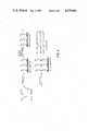
- FIG. 1is a schematic representation of the stepwise formation of an adsorbed multilayer film
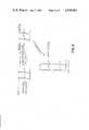
- FIG. 2illustrates multilayer formation by adsorption: binding through the O--Si--O function using bifunctional silane surfactants as monolayer building units:
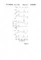
- FIG. 3illustrates IR ATR spectra for layers on silicon plate (45°, 17 reflections) measured with a Nicolet MX-1 Fourier transform spectrophotometer: (a) HTS/Si monolayer; (b) HTS/Si activated monolayer; (c) subtraction (b)-(a); (d) OTS/HTS/Si bilayer; (e) OTS second monolayer, subtraction (d)-(b); (f) OTS/Si monolayer.
- OTSis n-octadecyltrichlorosilane
- HTSis 15-hexadecenyltrichlorosilane.
- FIG. 4illustrates Spectra as in FIG. 3 for the following structures: (a) HTS/HTS/Si bilayer; (b) HTS/HTS/Si activated bilayer; (c) subtraction (b)-(a); (d) OTS/HTS/HTS/Si trilayer; (e) OTS third monolayer, subtraction (d)-(b); (f) OTS/Si monolayer.
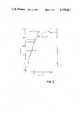
- FIG. 5is a plot of experimental vs. readings from ellipsometric measurements on silicon: -- , adsorbed silane films; - - - , LB films of Cd 2+ arachidate (C 20 ) deposited onto an adsorbed OTS monolayer.
- Such reactionsmay be intralayer, interlayer, or at the outer surface of the layer, may involve reagents in liquid, gas, or solid phases, electromagnetic radiation of any wavelength, ⁇ , ⁇ , ⁇ radiation, electron, molecular, or ionic beams, electrochemical processes, catalytic processes, etc.
- reactionexamples include oxidations (such as ozonations, permanganate action, etc.), reductions (such as reduction of ketones by sodium borohydride, etc.), condensations (such as amine-aldehyde, etc.), aromatic substitutions, ester and amide bond formation or hydrolysis (including esters of acids such as phosphoric, boric, boronic, sulfuric, sulfonic, etc.), salt formation, hydrogen bonding, complexations, polymerizations (intralayer and interlayer), organometalic couplings (including metals in the gas phase such as Grignard reactions with gaseous Mg), etc.
- oxidationssuch as ozonations, permanganate action, etc.
- reductionssuch as reduction of ketones by sodium borohydride, etc.
- condensationssuch as amine-aldehyde, etc.
- aromatic substitutionssuch as amine-aldehyde, etc.
- ester and amide bond formation or hydrolysisincluding esters of acids such as phosphoric, bo
- the method of the inventionmay also be used for the production of monolayers with desired surface properties.
- a monolayer of the type defined abovethe non-polar groups or the unsaturated functionality may be modified subsequently so as to impart to the layer, and thus to the surface, desired new properties, Amongst other uses this may be used for bonding together two such surfaces or for other adhesive effects.
- Surfaces according to the inventionof varying complementary properties, can be used for the bonding together of composite materials. Suitable complementary groups are for example aldehyde and amino groups; also hydrazide and acyl-halide groups may be used.
- the novel processcan be obtaining a layer having catalytic properties.
- biologically active compoundssuch as proteins (enzymes, antigens or the like).
- the chlorination step Awas carried out according to the method of Hooz and Gilani (J. Hooz and S. S. H. Gilani, Can. J. Chem., 46 (1968), 86) using either tri-n-butyl phosphine or triphenyl phosphine.
- the Grignard reaction Bwas conducted iin tetrahydrofuran (THF) with dibromoethane as entraining agent.
- Ethylene oxide or trimethylene oxidewas added dropwise with ice cooling to the Grignard reagent (step C); the mixture was then stirred at room temperature for 24 h, refluxed for another 2 h and finally quenched with a saturated aqueous solution of NH 4 Cl.
- Step Dwas performed by dropwise addition of the Grignard reagent to a magnetically stirred solution of SiCl 4 (in excess) in benzene. After stirring at ambient temperature for 2 h the mixture was refluxed for another 2 h, the solid material (MgCl 2 ) was then separated by centrifugation and the final product was vacuum distilled in a rotating-ball tube oven.
- STEP BMonolayer formation, surface chemical modification and multilayer formation
- Monolayerswere chemisorbed at ambient temperature from stirred solutions of the silane compounds concentration, froim 2.0 ⁇ 10 -3 to 5.0 ⁇ 10 -2 M) in a solvent mixture of 80%n-hexadecane-12%CCl 4 -8%CHCl 3 (J. Sagiv, J. Am. Chem. Soc. 102 (1980), 92). All solvents were passed through columns of alumina (Woelm-Pharma, W200 super, basic) and the chloroform was stabilized with absolute ethanol (1 vol.%). The solid substrates were immersed in the silane solutions for 1-2 min, with a subsequent quick withdrawal. Good monolayers were considered to be formed only on those substrates emerging dry from the silane solution (oleophobic)(Ibid.) The monolayer-covered substrates were rinsed with chloroform and distilled water, to ensure stability of the formed films.
- the modification of the outer vinylic groups into terminal hydroxylswas accomplished using the following procedure. Film-coated substrates were dipped for 1 min into a solution of diborane in THF (1M, Aldrich) kept under dry argon at room temperature, were then dipped for 1 min into an alkaline hydrogen peroxide solution (30% H 2 O 2 in 0.1M Aqueous NaOH) and finally were rinsed with distilled water and dried in a stream of air.
- the solid substrates employed in this workwere glass slides, mirrors of aluminium evaporated on glass slides, and silicon ATR plates.
- the glass slideswere cleaned ultrasonically for about 15 min in a boiling ethanol:chloroform mixture (1:1 by volume), rinsed with chloroform, dried in a stream of air and, before use, plasma treated for about 15 min in an r.f. argon plasma (Harrick PDC-3xG plasma cleaner).
- Aluminium(wire, 99.99% pure) was slowly evaporated on cleaned glass slides from a distance of 25 cm using an Edwards coating system at 10 -5 -10 -6 Torr.
- the aluminium mirrorswere plasma cleaned before coating with monolayer films as well as before blank measurements were performed.
- the silicon ATR plateswere cleaned using the same procedure as was described for the glass slides. Their degree of cleanness was monitored by IR specgroscopy (disappearance of the strong C--H stretching bands around 2900 cm -1 ) before monolayer coating.
- the removal of monolayer films from the silicon plates for their reuserequired prolonged exposure to oxygen and argon plasma treatments.
- Advancing contact angles for n-hexadecxane and H 2 Owere measured under ambient conditions with an NRL contact angle goniometer (Rame-Hart 100) using the sessile drop method.
- the reported datarefer to maximal values observed on the respective samples, and the precision of the measurements is of the order of ⁇ 1° for n-hexadecane and ⁇ 2° for H 2 O.
- the ellipsometric measurementswere performed according to the method described in F. L. McCrackin et al. J. Res. Natl. Bur. Stand., Sect. A, 67 (1963), 363, with a Rudolph research instrument (model 433) set at an angle of incidence of 64.10°.
- the 5461 A green line of a mercury lampwas used as the light source.
- IR measurementswere performed with a single-beam Fourier transform IR spectrophotometer (Nicolet MX-1). All reported spectra represent net absorbances due to the deposited surface films and were obtained by mathematical subtraction of the curves recorded with the clean substrates from the curves recorded after coating the substrates with the respective films.
- a Harrick variable-angle multiple-internal-reflection (ATR) attachment set at an angle of incidence of 45°was used for recording the ATR spectra.
- the internal reflection elementswere silicon single-pass plates (45°, 50 mm ⁇ 5 mm ⁇ 3 mm, 17 reflections).
- the multiple-external-reflection-absorption (RA) spectrawere recorded using two parallel Al/glass mirrors (76 mm ⁇ 13 mm) separated by a spacer 3 mm thick mounted into the same accessory as was used for the ATR measurements.
- the angle of incidencewas set at the maximal value possible with this attachment (75°), and the mirrors were displaced laterally with respect to each other by 11 mm.
- PTSpentadecenyltrichlorosilane
- TTStetradecenyltrichlorosilane
- HTShexadecenyltrichlorosilane
- HTSforms the monolayers with the highest degree of chain density and order within the series of presently synthesized silanes without, however, reaching the highest value possible for monolayers of this type. This suggests that longer chains are required (18-20 carbon atoms) to obtain bifunctional silane monolayers of the same quality as OTS or 17-octadecenoic acid films.
- Table IIgives the contact angles measured on a growing HTS film on glass. The expected periodicity in the contact angle values, reflecting the alternating polar-non-polar character of the film's outer surface during the two-step monolayer deposition process is actually observed.
- OTSorganic compound-semiconductor
- the monotonic decrease in the contact angles with increasing number of monolayers in the growing HTS filmreflects a tendency of deterioration of the molecular organization within each additional monolayer, probably as a result of accumulation of defects and structural irregularities.
- the high contact angles exhibited by the fifth OTS layerare in remarkable contrast with the general tendency observed for HTS films. This demonstrates the ability of OTS to bridge over irregularities and to form good monolayers even on molecularly "rough" surfaces. This interpretation is sustained by the observed inability of TTS and PTS to form oleophobic multilayer films, while good OTS/TTS and OTS/PTS bilayers could be produced without difficulty.
- the relationship between the ellipsometric angles ⁇ and ⁇ and the film thicknessis approximately linear for film thicknesses in the range from 0 to about 100 A.
- bifunctional silanes longer than HTS by two to four carbon atomsyield organized multilayer films in which the basic monolayer structure is preserved indepndent of thetotal number of deposited monolayers of their location within the film.
- high quality adsorbed filmsof any desired thickness.
Landscapes
- Engineering & Computer Science (AREA)
- Physics & Mathematics (AREA)
- General Physics & Mathematics (AREA)
- Condensed Matter Physics & Semiconductors (AREA)
- Chemical & Material Sciences (AREA)
- Manufacturing & Machinery (AREA)
- Computer Hardware Design (AREA)
- Microelectronics & Electronic Packaging (AREA)
- Power Engineering (AREA)
- Nanotechnology (AREA)
- Crystallography & Structural Chemistry (AREA)
- Materials Engineering (AREA)
- Composite Materials (AREA)
- Spectroscopy & Molecular Physics (AREA)
- Life Sciences & Earth Sciences (AREA)
- Wood Science & Technology (AREA)
- Organic Chemistry (AREA)
- Application Of Or Painting With Fluid Materials (AREA)
Abstract
Description
TABLE I ______________________________________ ADVANCING CONTACT ANGLES MEASURED ON SILANE MONOLAYERS ADSORBED ON GLASS Contact angle OTS HTS PTS TTS UTS Test Liquid (C.sub.18, saturated) (C.sub.16) (C.sub.15) (C.sub.14) (C.sub.11) ______________________________________ n-hexadecane 45° 40° 38° 40° Spreads H.sub.2 O 110° 105° 97° 105° 90° ______________________________________
TABLE II __________________________________________________________________________ADVANCING CONTACT ANGLES MEASURED ON A GROWING MULTILAYER FILM ON GLASS Contact angle First layer Second layer Third layer Fourth layer Fifth layer Test liquid HTS HTS activated HTS HTS activated HTS HTS activated HTS HTS activated OTS __________________________________________________________________________n-hexadecane 40° 0° 37° 0° 32° 0° 26° 0° 45° H.sub.2 O 105° 50° 99° 50° 96° 50° 94° 50° 107° __________________________________________________________________________
TABLE III ______________________________________ ADVANCING CONTACT ANGLES MEASURED ON GROWING MULTILAYER FILMS ON SILICON Contact angle FIGS. Film n-hexadecane H.sub.2 O -- ______________________________________ HTS/Si 35° 100° 3(a), 5 HTS/Si activated 0° 48° 3(b) OTS/HTS/Si 45° 108° 3(d), 5 HTS/Si 40° 105° -- HTS/Si activated 0° 50° -- HTS/HTS/Si 34° 98° 4(a), 5 HTS/HTS/Si activated 0° 50° 4(b) OTS/HTS/HTS/Si 44° 105° 4(d), 5 OTS/Si 46° 111° 3(f), 4(f), 5 ______________________________________
TABLE IV __________________________________________________________________________DENSITY OF MOLECULES IN ADSORBED FILMS ON SILICON RELATIVE TO THAT FOR A CLOSELY PACKED OCTADECYLTRICHLOROSILANE MONOLAYER.sup.a Adsorbance per-CH.sub.2 -- Relative group at 2918.5 cm.sup.-1 surface Film (×10.sup.3) coverage (%) FIGS. __________________________________________________________________________OTS first layer = OTS/Si 2.61 100 3(f), 4(f) OTS second layer = 2.23 85 3(e) (OTS/HTS/Si)--(HTS/Si activated) OTS third layer = 2.06 79 4(e) (OTS/HTS/HTS/Si)--(HTS/HTS/Si activated) HTS/HTS/Si 1.82 70 4(a) HTS/HTS/Si activated 1.84 71 4(b) HTS/Si 1.64 63 3(a) HTS/Si activated 1.63 62 3(b) __________________________________________________________________________ .sup.a Data calculated from IR ATR spectra
Claims (15)
Priority Applications (1)
| Application Number | Priority Date | Filing Date | Title |
|---|---|---|---|
| US06/530,102US4539061A (en) | 1983-09-07 | 1983-09-07 | Process for the production of built-up films by the stepwise adsorption of individual monolayers |
Applications Claiming Priority (1)
| Application Number | Priority Date | Filing Date | Title |
|---|---|---|---|
| US06/530,102US4539061A (en) | 1983-09-07 | 1983-09-07 | Process for the production of built-up films by the stepwise adsorption of individual monolayers |
Publications (1)
| Publication Number | Publication Date |
|---|---|
| US4539061Atrue US4539061A (en) | 1985-09-03 |
Family
ID=24112452
Family Applications (1)
| Application Number | Title | Priority Date | Filing Date |
|---|---|---|---|
| US06/530,102Expired - Fee RelatedUS4539061A (en) | 1983-09-07 | 1983-09-07 | Process for the production of built-up films by the stepwise adsorption of individual monolayers |
Country Status (1)
| Country | Link |
|---|---|
| US (1) | US4539061A (en) |
Cited By (205)
| Publication number | Priority date | Publication date | Assignee | Title |
|---|---|---|---|---|
| US4618561A (en)* | 1983-12-06 | 1986-10-21 | Canon Kabushiki Kaisha | Monomolecular record memory medium with photosensitive diazonium salt |
| US4636767A (en)* | 1985-08-21 | 1987-01-13 | The United States Of America As Represented By The Secretary Of The Navy | Mixed semiconductor film device for monitoring gases |
| US4686169A (en)* | 1984-11-13 | 1987-08-11 | Matsushita Electric Industrial Co., Ltd. | Optical recording medium and production of the same |
| US4693915A (en)* | 1984-04-20 | 1987-09-15 | Canon Kabushiki Kaisha | Film forming method, recording medium formed thereby and recording method therewith |
| US4715929A (en)* | 1985-07-19 | 1987-12-29 | Matsushita Electric Industrial Co., Ltd. | Pattern forming method |
| US4756971A (en)* | 1984-12-28 | 1988-07-12 | Ksv-Chemicals Oy | Surface treatment agents and polymers comprising substituted phenyl silanes and siloxanes |
| US4766047A (en)* | 1983-10-14 | 1988-08-23 | Canon Kabushiki Kaisha | Optical recording medium and optical recording process using such medium |
| EP0249457A3 (en)* | 1986-06-12 | 1988-09-28 | Matsushita Electric Industrial Co., Ltd. | Method for formation of patterns |
| US4796971A (en)* | 1987-09-28 | 1989-01-10 | Eastman Kodak Company | Optical article containing a polymeric matrix exhibiting a high level of second order polarization susceptibility |
| US4798740A (en)* | 1986-03-31 | 1989-01-17 | Canon Kabushiki Kaisha | Polymerizable film and pattern forming method by use thereof |
| US4818665A (en)* | 1984-03-14 | 1989-04-04 | Canon Kabushiki Kaisha | Medium and process for image formation |
| US4875759A (en)* | 1984-11-19 | 1989-10-24 | Matsushita Electric Industrial Co., Ltd. | Optical fiber and method of producing the same |
| EP0322233A3 (en)* | 1987-12-21 | 1990-07-18 | Matsushita Electric Industrial Co., Ltd. | Method for producing ultrathin metal film and ultrathin-thin metal pattern |
| US4957851A (en)* | 1985-04-16 | 1990-09-18 | Canon Kabushiki Kaisha | Image recording medium comprising a diacetylene derivative compound film and a radiation absorbing layer |
| US4960679A (en)* | 1985-01-31 | 1990-10-02 | Canon Kabushiki Kaisha | Image forming device |
| US4960722A (en)* | 1985-08-29 | 1990-10-02 | Matsushita Electric Industrial Co., Ltd. | Sensor using a field effect transistor and method of fabricating the same |
| EP0351092A3 (en)* | 1988-06-28 | 1990-10-10 | Matsushita Electric Industrial Co., Ltd. | Method for the formation of monomolecular adsorption films or built-up films of monomolecular layers using silane compounds having an acetylene or diacetylene bond |
| EP0386784A3 (en)* | 1989-03-09 | 1990-12-19 | Matsushita Electric Industrial Co., Ltd. | Permselective membrane and process for producing the same |
| US5018829A (en)* | 1984-11-19 | 1991-05-28 | Matsushita Electric Industrial Co., Ltd. | Optical fiber and method of producing the same |
| US5057339A (en)* | 1988-12-29 | 1991-10-15 | Matsushita Electric Industrial Co., Ltd. | Metallized polyacetylene-type or polyacene-type ultralong conjugated polymers and process for producing the same |
| US5077085A (en)* | 1987-03-06 | 1991-12-31 | Schnur Joel M | High resolution metal patterning of ultra-thin films on solid substrates |
| US5079600A (en)* | 1987-03-06 | 1992-01-07 | Schnur Joel M | High resolution patterning on solid substrates |
| US5093154A (en)* | 1988-09-05 | 1992-03-03 | Matsushita Electric Industrial Co., Ltd. | Process for preparing a monomolecular built-up film |
| US5108573A (en)* | 1990-06-05 | 1992-04-28 | The United States Of America As Represented By The United States Department Of Energy | Morphology in electrochemically grown conducting polymer films |
| EP0482613A1 (en)* | 1990-10-25 | 1992-04-29 | Matsushita Electric Industrial Co., Ltd. | A fluorocarbon-based coating film and method of manufacturing the same |
| EP0484886A1 (en)* | 1990-11-06 | 1992-05-13 | Matsushita Electric Industrial Co., Ltd. | Fluorocarbon-based polymer lamination coating film and method of manufacturing the same |
| EP0491251A1 (en)* | 1990-12-10 | 1992-06-24 | Matsushita Electric Industrial Co., Ltd. | Adsorbed monomolecular film and method of manufacturing the same |
| EP0498335A1 (en)* | 1991-02-06 | 1992-08-12 | Matsushita Electric Industrial Co., Ltd. | Method of manufacturing chemically adsorbed film |
| US5143750A (en)* | 1990-12-21 | 1992-09-01 | Matsushita Electric Industrial Co., Ltd. | Method of manufacturing chemically adsorbed film |
| US5156918A (en)* | 1991-03-28 | 1992-10-20 | Northwestern University | Self-assembled super lattices |
| EP0484746A3 (en)* | 1990-10-25 | 1992-10-28 | Matsushita Electric Industrial Co., Ltd | Chemically adsorbed monomolecular lamination film and method of manufacturing the same |
| EP0493747A3 (en)* | 1990-12-25 | 1992-11-04 | Matsushita Electric Industrial Co., Ltd. | Anti-contaminating adsorbed film and method of manufacturing the same |
| EP0511590A1 (en)* | 1991-04-30 | 1992-11-04 | Matsushita Electric Industrial Co., Ltd. | Functional laminated chemically adsorbed films and methods of manufacturing the same |
| EP0511657A2 (en) | 1991-04-30 | 1992-11-04 | Matsushita Electric Industrial Co., Ltd. | Hydrophilic chemically adsorbed film and method of manufacturing the same |
| EP0497189A3 (en)* | 1991-01-23 | 1992-11-04 | Matsushita Electric Industrial Co., Ltd. | Water- and oil-repelling absorbed film and method of manufacturing the same |
| EP0472990A3 (en)* | 1990-08-25 | 1993-01-07 | Bayer Ag | Mono or multilayer deposits on a substrat and process for making them |
| EP0492545A3 (en)* | 1990-12-25 | 1993-01-20 | Matsushita Electric Industrial Co., Ltd. | Transparent substrate with monomolecular film thereon and method of manufacturing the same |
| EP0523502A1 (en)* | 1991-07-17 | 1993-01-20 | Matsushita Electric Industrial Co., Ltd. | Chemically adsorbed film and method of manufacturing the same |
| EP0497204A3 (en)* | 1991-01-28 | 1993-01-27 | Matsushita Electric Industrial Co., Ltd. | Medical member and method of manufacturing the same |
| EP0524529A1 (en)* | 1991-07-23 | 1993-01-27 | Matsushita Electric Industrial Co., Ltd. | Hydrophylic substrate and method of manufacturing the same |
| EP0525598A1 (en)* | 1991-07-26 | 1993-02-03 | Matsushita Electric Industrial Co., Ltd. | Water-and oil repellent susbtrate and method of treatment |
| US5204126A (en)* | 1990-02-06 | 1993-04-20 | Nanofilm Corporation | Mold surfaces with ultra thin release films |
| EP0547550A1 (en)* | 1991-12-16 | 1993-06-23 | Matsushita Electric Industrial Co., Ltd. | Method of manufacturing a chemically adsorbed film |
| US5234718A (en)* | 1991-02-19 | 1993-08-10 | Matsushita Electric Industrial Co., Ltd. | Method of manufacturing a chemically adsorbed film |
| US5239608A (en)* | 1988-12-16 | 1993-08-24 | U.S. Philips Corp. | Magneto-optical waveguide |
| US5240747A (en)* | 1989-05-11 | 1993-08-31 | Kanegafuchi Kagaku Kogyo Kabushiki Kaisha | Process for modifying surfaces of materials |
| US5246740A (en)* | 1990-01-12 | 1993-09-21 | Matsushita Electric Industrial Co., Ltd. | Process for preparing a lamination of organic monomolecular films, and a chemical adsorbent used for the process |
| US5248526A (en)* | 1988-04-28 | 1993-09-28 | Matsushita Electric Industrial Co., Ltd. | Process for producing polyacetylene or polyacene type long conjugated polymers |
| US5260004A (en)* | 1991-12-02 | 1993-11-09 | The United States Of America As Represented By The Secretary Of The Army | Process of making Langmuir-Blodgett films having photo-electronic properties |
| US5268211A (en)* | 1991-01-17 | 1993-12-07 | Matsushita Electric Industrial Co., Ltd. | Optical recording medium |
| US5277980A (en)* | 1988-06-07 | 1994-01-11 | Matsushita Electric Industrial Co., Ltd. | Mass of fine particles of inorganic material and a film of the fine inorganic particles |
| EP0582181A1 (en)* | 1992-07-29 | 1994-02-09 | Matsushita Electric Industrial Co., Ltd. | Lubricating film and method of manufacturing the same |
| EP0582131A1 (en)* | 1992-07-29 | 1994-02-09 | Matsushita Electric Industrial Co., Ltd. | Lubricating film and method of manufacturing the same |
| US5302416A (en)* | 1988-04-28 | 1994-04-12 | Matsushita Electric Industrial Co., Ltd. | Process for producing polyacetylene or polyacene type long conjugated polymers |
| US5304583A (en)* | 1988-04-28 | 1994-04-19 | Matsushita Electric Industrial Co., Ltd. | Process for producing polyacetylene or polyacene type long conjugated polymers |
| US5304582A (en)* | 1988-04-28 | 1994-04-19 | Matsushita Electric Industrial Co., Ltd. | Process for producing polyacetylene or polyacene type long conjugated polymers |
| EP0481362A3 (en)* | 1990-10-10 | 1994-05-11 | Yeda Res & Dev | Composite organic-inorganic superlattices |
| EP0598361A1 (en)* | 1992-11-18 | 1994-05-25 | Rouvain M. Bension | Initiation and bonding of diamond and other thin films |
| US5316784A (en)* | 1989-07-14 | 1994-05-31 | Boehringer Mannheim Gmbh | Process for the production of a solid phase matrix coated with an immunologically active substance |
| US5338579A (en)* | 1992-05-27 | 1994-08-16 | Matsushita Electric Industrial Co., Ltd. | Method of manufacturing a chemically adsorbed film |
| US5356433A (en)* | 1991-08-13 | 1994-10-18 | Cordis Corporation | Biocompatible metal surfaces |
| US5372888A (en)* | 1991-02-06 | 1994-12-13 | Matsushita Electric Industrial Co., Ltd. | Chemically adsorbed film and method of manufacturing the same |
| US5378521A (en)* | 1992-09-12 | 1995-01-03 | Matsushita Electric Industrial Co., Ltd. | Water-and oil-repelling members and method of manufacturing the same |
| EP0629673A3 (en)* | 1991-01-23 | 1995-01-18 | Matsushita Electric Industrial Co Ltd | |
| US5397642A (en)* | 1992-04-28 | 1995-03-14 | The United States Of America As Represented By The United States Department Of Energy | Articles including thin film monolayers and multilayers |
| US5402262A (en)* | 1992-08-19 | 1995-03-28 | Hoechst Aktiengesellschaft | Layer element having a plurality of monomolecular layers |
| US5436033A (en)* | 1991-07-15 | 1995-07-25 | Matsushita Electric Industrial Co., Ltd. | Method of manufacturing a polymer ultra thin film electret |
| US5443901A (en)* | 1991-02-05 | 1995-08-22 | Matsushita Electric Industrial Co., Ltd. | Magnetic recording medium having an adsorbed film of molecules comprising two species of straight carbon chain molecules |
| US5445886A (en)* | 1988-07-04 | 1995-08-29 | Matsushita Electric Industrial Co., Ltd. | Structure having a surface covered with a monomolecular film |
| US5449554A (en)* | 1992-08-31 | 1995-09-12 | Matsushita Electric Industrial Co., Ltd. | Antistatic film and method of manufacturing the same |
| EP0628819A3 (en)* | 1993-06-08 | 1995-09-27 | Bayer Ag | Coated carrier, method for manufacturing it and its use in immobilising biomolecules on the surfaces of solids. |
| WO1996002383A1 (en)* | 1994-07-14 | 1996-02-01 | Competitive Technologies, Inc. | Stepwise formation of multilayered nanostructures from macromolecular precursors |
| US5512328A (en)* | 1992-08-07 | 1996-04-30 | Hitachi, Ltd. | Method for forming a pattern and forming a thin film used in pattern formation |
| US5545432A (en)* | 1993-04-08 | 1996-08-13 | Case Western Reserve University | Synthesis of metal oxide thin films |
| US5552236A (en)* | 1992-03-16 | 1996-09-03 | Matsushita Electric Industrial Co., Ltd. | Organic magnetic film and method of manufacturing the same |
| DE19532355A1 (en)* | 1995-03-24 | 1996-09-26 | Hewlett Packard Co | Treatment of an orifice plate with self-assembled chemical compounds forming monolayers |
| US5607475A (en)* | 1995-08-22 | 1997-03-04 | Medtronic, Inc. | Biocompatible medical article and method |
| US5652059A (en)* | 1991-11-20 | 1997-07-29 | Bar Ilan University | Method for attaching microspheres to a substrate |
| WO1997038802A1 (en)* | 1996-04-12 | 1997-10-23 | The Texas A & M University System | Polymeric self-assembled mono- and multilayers and their use in photolithography |
| US5686549A (en)* | 1993-03-25 | 1997-11-11 | Research Corporation Technologies, Inc. | Polymers useful in forming self-assembled bonded anisotropic ultrathin layers and their use |
| US5736245A (en)* | 1994-06-17 | 1998-04-07 | Lucent Technologies Inc. | Chemical treatment for silica-containing glass surfaces |
| US5766698A (en)* | 1996-11-25 | 1998-06-16 | Nanofilm Corporation | Method for modifying surfaces with ultra thin films |
| US5780148A (en)* | 1992-11-12 | 1998-07-14 | Matsushita Electric Industrial Co., Ltd. | Hydrophilic thin film and method of manufacturing the same |
| US5783299A (en)* | 1986-01-21 | 1998-07-21 | Seiko Epson Corporation | Polarizer plate with anti-stain layer |
| US5846279A (en)* | 1996-04-04 | 1998-12-08 | Matsushita Electric Industrial Co., Ltd. | Process for producting a contamination-resistant float glass |
| US5851674A (en)* | 1997-07-30 | 1998-12-22 | Minnesota Mining And Manufacturing Company | Antisoiling coatings for antireflective surfaces and methods of preparation |
| US5869136A (en)* | 1992-02-27 | 1999-02-09 | Matsushita Electric Industrial Co., Ltd. | Method of manufacturing a chemically adsorbed multilayer film |
| US6033774A (en)* | 1994-12-14 | 2000-03-07 | Northwestern University | Self-assembled superlattices and waveguides prepared for use therewith |
| WO2000025938A1 (en)* | 1998-11-03 | 2000-05-11 | Diamon-Fusion International, Inc. | Capped silicone film and method of manufacture thereof |
| US6079276A (en)* | 1995-02-28 | 2000-06-27 | Rosemount Inc. | Sintered pressure sensor for a pressure transmitter |
| US6114099A (en)* | 1996-11-21 | 2000-09-05 | Virginia Tech Intellectual Properties, Inc. | Patterned molecular self-assembly |
| US6130044A (en)* | 1994-02-11 | 2000-10-10 | Institut Pasteur And Centre National De La Recherche Scientifique | Surfaces for biological reactions, process for preparing them and process for their use |
| US6171652B1 (en) | 1998-05-26 | 2001-01-09 | Brij P. Singh | Method for modifying surfaces with ultra thin films |
| US6207578B1 (en)* | 1999-02-19 | 2001-03-27 | Micron Technology, Inc. | Methods of forming patterned constructions, methods of patterning semiconductive substrates, and methods of forming field emission displays |
| US6248537B1 (en) | 1999-05-28 | 2001-06-19 | Institut Pasteur | Use of the combing process for the identification of DNA origins of replication |
| EP1110622A1 (en)* | 1999-12-22 | 2001-06-27 | Eastman Kodak Company | Method for replenishing coatings on printhead nozzle plate |
| US6258454B1 (en)* | 1998-09-01 | 2001-07-10 | Agilent Technologies Inc. | Functionalization of substrate surfaces with silane mixtures |
| US6277444B1 (en)* | 1992-03-02 | 2001-08-21 | Matsushita Electric Industrial Co., Ltd. | Chemically adsorber film and method of manufacturing the same |
| US6277485B1 (en) | 1998-01-27 | 2001-08-21 | 3M Innovative Properties Company | Antisoiling coatings for antireflective surfaces and methods of preparation |
| JP3244298B2 (en) | 1991-04-30 | 2002-01-07 | 松下電器産業株式会社 | Antistatic chemisorption monomolecular film and method for producing the same |
| JP3244299B2 (en) | 1991-04-30 | 2002-01-07 | 松下電器産業株式会社 | Hydrophilic chemisorption monomolecular film and method for producing the same |
| USRE37698E1 (en)* | 1990-10-25 | 2002-05-14 | Matsushita Electric Industrial Co. | Method of manufacturing a fluorocarbon-based coating film |
| JP3292205B2 (en) | 1991-04-30 | 2002-06-17 | 松下電器産業株式会社 | Functional chemisorption membrane and method for producing the same |
| US20020133072A1 (en)* | 1999-09-10 | 2002-09-19 | Guo-Bin Wang | Graft polymerization of substrate surfaces |
| EP1118465A3 (en)* | 1999-12-22 | 2002-11-13 | Eastman Kodak Company | Replenishable hydrophobic coating for printhead nozzle plate |
| US6484585B1 (en) | 1995-02-28 | 2002-11-26 | Rosemount Inc. | Pressure sensor for a pressure transmitter |
| US6503567B2 (en) | 1990-12-25 | 2003-01-07 | Matsushita Electric Industrial Co., Ltd. | Transparent substrate and method of manufacturing the same |
| US6505516B1 (en) | 2000-01-06 | 2003-01-14 | Rosemount Inc. | Capacitive pressure sensing with moving dielectric |
| US6508129B1 (en) | 2000-01-06 | 2003-01-21 | Rosemount Inc. | Pressure sensor capsule with improved isolation |
| US6516671B2 (en) | 2000-01-06 | 2003-02-11 | Rosemount Inc. | Grain growth of electrical interconnection for microelectromechanical systems (MEMS) |
| US6520020B1 (en) | 2000-01-06 | 2003-02-18 | Rosemount Inc. | Method and apparatus for a direct bonded isolated pressure sensor |
| US6521334B1 (en)* | 1990-12-25 | 2003-02-18 | Matsushita Electric Industrial Co., Ltd. | Transparent substrate and method of manufacturing the same |
| US20030044798A1 (en)* | 2001-08-31 | 2003-03-06 | Lefkowitz Steven M. | Methods for generating ligand arrays via deposition of ligands onto olefin displaying substrates, and arrays produced thereby |
| US6561038B2 (en) | 2000-01-06 | 2003-05-13 | Rosemount Inc. | Sensor with fluid isolation barrier |
| US20030102471A1 (en)* | 2001-11-05 | 2003-06-05 | Kelley Tommie W. | Organic thin film transistor with polymeric interface |
| US20030129312A1 (en)* | 1999-03-19 | 2003-07-10 | Fryxell Glen E. | Self-assembled monolayer and method of making |
| US6610363B2 (en) | 2000-10-18 | 2003-08-26 | Nanofilm, Ltd. | Composition with film forming alkylsilsesquioxane polymer and method for applying hydrophobic films to surfaces |
| WO2003077327A1 (en)* | 2002-03-07 | 2003-09-18 | 3M Innovative Properties Company | Organic thin film transistors with modified surface of gate-dielectric |
| WO2003023877A3 (en)* | 2001-09-06 | 2003-09-25 | 3M Innovative Properties Co | Surface modifying layers for organic thin film transistors |
| US20030203110A1 (en)* | 2000-10-18 | 2003-10-30 | Arora Pramod K. | Composition with film forming alkylsilsesquioxane polymer and method for applying hydrophobic films to surfaces |
| US20030219597A1 (en)* | 2002-03-13 | 2003-11-27 | Regents Of The University Of Minnesota | Silica-based materials and methods |
| US6660338B1 (en) | 2001-03-08 | 2003-12-09 | Agilent Technologies, Inc. | Functionalization of substrate surfaces with silane mixtures |
| US20040001943A1 (en)* | 1999-03-19 | 2004-01-01 | Alford Kentin L. | Methods of making monolayers |
| US20040053037A1 (en)* | 2002-09-16 | 2004-03-18 | Koch Carol A. | Layer by layer assembled nanocomposite barrier coatings |
| US20040063098A1 (en)* | 2002-09-26 | 2004-04-01 | Hargreaves John S. | Methods for producing multilayer ligand arrays |
| US6740409B1 (en) | 2000-11-15 | 2004-05-25 | Board Of Trustees Of University Of Illinois | Polymer films |
| US6743516B2 (en) | 2000-09-29 | 2004-06-01 | Guardian Industries Corporation | Highly durable hydrophobic coatings and methods |
| US20040157047A1 (en)* | 2003-02-06 | 2004-08-12 | Ali Mehrabi | Continuous process for manufacturing electrostatically self-assembled coatings |
| US20040198898A1 (en)* | 2001-08-03 | 2004-10-07 | Arora Pramod K. | Method for vapor deposition of hydrophobic films on surfaces |
| US6805904B2 (en) | 2002-02-20 | 2004-10-19 | International Business Machines Corporation | Process of forming a multilayer nanoparticle-containing thin film self-assembly |
| US20040224095A1 (en)* | 2003-05-08 | 2004-11-11 | Texas Instruments Incorporated | Hydrophobic coating for oxide surfaces |
| US20040221807A1 (en)* | 2003-05-09 | 2004-11-11 | Mohith Verghese | Reactor surface passivation through chemical deactivation |
| US20040236399A1 (en)* | 2003-04-22 | 2004-11-25 | Medtronic Vascular, Inc. | Stent with improved surface adhesion |
| US6848316B2 (en) | 2002-05-08 | 2005-02-01 | Rosemount Inc. | Pressure sensor assembly |
| US20050042612A1 (en)* | 2001-07-30 | 2005-02-24 | Hubbard Michael Anthony | Graft polymer martrices |
| WO2005060668A3 (en)* | 2003-12-18 | 2005-09-15 | Univ Columbia | Methods of modifying surfaces |
| US20050271808A1 (en)* | 2004-03-25 | 2005-12-08 | Nomadics, Inc. | Process and apparatus for layer by layer assembly of reinforced composite materials |
| US20060003438A1 (en)* | 2004-06-17 | 2006-01-05 | Engstrom James R | Growth of inorganic thin films using self-assembled monolayers as nucleation sites |
| WO2006039507A2 (en) | 2004-10-01 | 2006-04-13 | Phenomenex, Inc. | Ph stable chromatographic media using templated multilayer organic/inorganic grafting |
| US20060100696A1 (en)* | 2004-11-10 | 2006-05-11 | Atanasoska Ljiljana L | Medical devices and methods of making the same |
| EP1670298A1 (en)* | 2004-12-07 | 2006-06-14 | Samsung SDI Germany GmbH | Substrate for a display and method for manufacturing the same |
| US20060135028A1 (en)* | 2004-12-07 | 2006-06-22 | Andreas Klyszcz | Substrate for a display and method for manufacturing the same |
| US20060160272A1 (en)* | 2003-06-20 | 2006-07-20 | Franz Effenberger | Synthesis method for a compound used to form a self-assembled monolayer, compound for forming a self-assembled monolayer, and layer structure for a semiconductor component |
| US20060165912A1 (en)* | 2003-02-13 | 2006-07-27 | Koberstein Jeffrey T | Micropatterning of molecular surfaces via selective irradiation |
| US20060175603A1 (en)* | 2003-06-20 | 2006-08-10 | Guenter Schmid | Compound used to form a self-assembled monolayer, layer structure, semiconductor component having a layer structure, and method for producing a layer structure |
| US20060216327A1 (en)* | 2005-03-28 | 2006-09-28 | Bacterin, Inc. | Multilayer coating for releasing biologically-active agents and method of making |
| US20060289115A1 (en)* | 2005-06-22 | 2006-12-28 | Changchun Institute Of Applied Chemistry Chinese Academy Of Science | Method for bonding two solid planes via surface assembling of active functional groups |
| US20070027467A1 (en)* | 2005-07-28 | 2007-02-01 | Ethicon Endo-Surgery, Inc. | Devices and methods for stricture dilation |
| US20070098894A1 (en)* | 2003-05-09 | 2007-05-03 | Mohith Verghese | Reactor surface passivation through chemical deactivation |
| US20070098902A1 (en)* | 2005-06-17 | 2007-05-03 | Cornell Research Foundation, Inc. | Fabricating inorganic-on-organic interfaces for molecular electronics employing a titanium coordination complex and thiophene self-assembled monolayers |
| US20080049326A1 (en)* | 2006-08-24 | 2008-02-28 | Hanson Eric L | Optical articles with thin hydrophobic layers |
| US20080086201A1 (en)* | 2006-09-15 | 2008-04-10 | Boston Scientific Scimed, Inc. | Magnetized bioerodible endoprosthesis |
| US20080171147A1 (en)* | 2007-01-17 | 2008-07-17 | Brij Pal Singh | Forming thin films using a resealable vial carrier of amphiphilic molecules |
| US20080176085A1 (en)* | 2006-09-21 | 2008-07-24 | Satoshi Tanaka | Hydrophilic composition and hydrophilic member |
| US20080241557A1 (en)* | 2007-03-28 | 2008-10-02 | Satoshi Hoshi | Hydrophilic member and undercoating composition |
| US7468206B1 (en) | 1996-12-19 | 2008-12-23 | Panasonic Corporation | Organic ultra-thin film |
| US20090029179A1 (en)* | 2007-05-14 | 2009-01-29 | Fujifilm Corporation | Two-liquid composition, hydrophilic composition and hydrophilic member |
| US20090077798A1 (en)* | 2007-09-21 | 2009-03-26 | Seiko Epson Corporation | Method for forming conductive post, method for manufacturing multilayered wiring substrate, and method for manufacturing electronic apparatus |
| US20090239051A1 (en)* | 2008-03-21 | 2009-09-24 | Makoto Fukuda | Hydrophilic composition and hydrophilic treated member |
| US20090255465A1 (en)* | 2004-08-18 | 2009-10-15 | Sheehan Paul E | Thermal control of deposition in dip pen nanolithography |
| US20090263605A1 (en)* | 2005-11-16 | 2009-10-22 | Satoshi Hoshi | Surface-hydrophilic structure |
| US20090274914A1 (en)* | 2005-11-17 | 2009-11-05 | Satoshi Hoshi | Hydrophilic member and process for producing the same |
| US20090297868A1 (en)* | 2008-05-27 | 2009-12-03 | Toppan Printing Co., Ltd. | Method for Forming Self-Assembled Monolayer Film, and Structural Body and Field-Effect Transistor Having Same |
| US20100072080A1 (en)* | 2008-05-05 | 2010-03-25 | The Regents Of The University Of California | Functionalized Nanopipette Biosensor |
| US20100276302A1 (en)* | 2007-02-02 | 2010-11-04 | Burkhard Raguse | Chemiresistor for use in conducting electrolyte solution |
| US20100311614A1 (en)* | 2002-08-16 | 2010-12-09 | Avantra Biosciences Corporation | Substrates for Isolating, Reacting and Microscopically Analyzing Materials |
| US7955382B2 (en) | 2006-09-15 | 2011-06-07 | Boston Scientific Scimed, Inc. | Endoprosthesis with adjustable surface features |
| US7985252B2 (en) | 2008-07-30 | 2011-07-26 | Boston Scientific Scimed, Inc. | Bioerodible endoprosthesis |
| US7998192B2 (en) | 2008-05-09 | 2011-08-16 | Boston Scientific Scimed, Inc. | Endoprostheses |
| US20110198736A1 (en)* | 2010-02-17 | 2011-08-18 | Asm America, Inc. | Reactive site deactivation against vapor deposition |
| US8002821B2 (en) | 2006-09-18 | 2011-08-23 | Boston Scientific Scimed, Inc. | Bioerodible metallic ENDOPROSTHESES |
| US8048150B2 (en) | 2006-04-12 | 2011-11-01 | Boston Scientific Scimed, Inc. | Endoprosthesis having a fiber meshwork disposed thereon |
| US8052744B2 (en) | 2006-09-15 | 2011-11-08 | Boston Scientific Scimed, Inc. | Medical devices and methods of making the same |
| US8052743B2 (en) | 2006-08-02 | 2011-11-08 | Boston Scientific Scimed, Inc. | Endoprosthesis with three-dimensional disintegration control |
| US8052745B2 (en) | 2007-09-13 | 2011-11-08 | Boston Scientific Scimed, Inc. | Endoprosthesis |
| US8057534B2 (en) | 2006-09-15 | 2011-11-15 | Boston Scientific Scimed, Inc. | Bioerodible endoprostheses and methods of making the same |
| US8080055B2 (en) | 2006-12-28 | 2011-12-20 | Boston Scientific Scimed, Inc. | Bioerodible endoprostheses and methods of making the same |
| US8089029B2 (en) | 2006-02-01 | 2012-01-03 | Boston Scientific Scimed, Inc. | Bioabsorbable metal medical device and method of manufacture |
| US8119445B2 (en) | 2008-05-27 | 2012-02-21 | The Board Of Trustees Of The Leland Stanford Junior University | Organic semiconductors and growth approaches therefor |
| US8128689B2 (en) | 2006-09-15 | 2012-03-06 | Boston Scientific Scimed, Inc. | Bioerodible endoprosthesis with biostable inorganic layers |
| US8236046B2 (en) | 2008-06-10 | 2012-08-07 | Boston Scientific Scimed, Inc. | Bioerodible endoprosthesis |
| EP0545201B2 (en)† | 1991-11-29 | 2012-08-22 | PPG Industries Ohio, Inc. | Durable water repellent glass surface |
| US8267992B2 (en) | 2009-03-02 | 2012-09-18 | Boston Scientific Scimed, Inc. | Self-buffering medical implants |
| US8303643B2 (en) | 2001-06-27 | 2012-11-06 | Remon Medical Technologies Ltd. | Method and device for electrochemical formation of therapeutic species in vivo |
| US8382824B2 (en) | 2008-10-03 | 2013-02-26 | Boston Scientific Scimed, Inc. | Medical implant having NANO-crystal grains with barrier layers of metal nitrides or fluorides |
| WO2013101896A1 (en) | 2011-12-30 | 2013-07-04 | Quest Diagnostics Investments Incorporated | Nucleic acid analysis using emulsion pcr |
| US20130260058A1 (en)* | 2002-12-14 | 2013-10-03 | Plastic Logic Limited | Electronic devices |
| US8668732B2 (en) | 2010-03-23 | 2014-03-11 | Boston Scientific Scimed, Inc. | Surface treated bioerodible metal endoprostheses |
| US20140134793A1 (en)* | 2010-03-12 | 2014-05-15 | Wisconsin Alumni Research Foundation | Methods for making large-area, free-standing metal oxide films |
| US8808726B2 (en) | 2006-09-15 | 2014-08-19 | Boston Scientific Scimed. Inc. | Bioerodible endoprostheses and methods of making the same |
| US8840660B2 (en) | 2006-01-05 | 2014-09-23 | Boston Scientific Scimed, Inc. | Bioerodible endoprostheses and methods of making the same |
| US9223203B2 (en) | 2011-07-08 | 2015-12-29 | Asm International N.V. | Microcontact printed films as an activation layer for selective atomic layer deposition |
| DE102015103335A1 (en)* | 2015-03-06 | 2016-09-08 | Osram Opto Semiconductors Gmbh | Optoelectronic device and method for producing an optoelectronic device |
| US9562288B2 (en) | 2013-04-24 | 2017-02-07 | Diamon Fusion International, Inc. | Defined dosing atmospheric temperature and pressure vapor deposition system |
| US9911595B1 (en)* | 2017-03-17 | 2018-03-06 | Lam Research Corporation | Selective growth of silicon nitride |
| US10043656B1 (en) | 2017-03-10 | 2018-08-07 | Lam Research Corporation | Selective growth of silicon oxide or silicon nitride on silicon surfaces in the presence of silicon oxide |
| US10176984B2 (en) | 2017-02-14 | 2019-01-08 | Lam Research Corporation | Selective deposition of silicon oxide |
| US10242866B2 (en) | 2017-03-08 | 2019-03-26 | Lam Research Corporation | Selective deposition of silicon nitride on silicon oxide using catalytic control |
| DE102017130528A1 (en)* | 2017-12-19 | 2019-06-19 | Osram Opto Semiconductors Gmbh | Optoelectronic component and method for producing an optoelectronic component |
| US10460930B2 (en) | 2017-11-22 | 2019-10-29 | Lam Research Corporation | Selective growth of SiO2 on dielectric surfaces in the presence of copper |
| US10559461B2 (en) | 2017-04-19 | 2020-02-11 | Lam Research Corporation | Selective deposition with atomic layer etch reset |
| EP3659634A1 (en) | 2018-11-29 | 2020-06-03 | Cook Medical Technologies LLC | Bioactive agent coated medical device and method of coating such a device |
| US11404275B2 (en) | 2018-03-02 | 2022-08-02 | Lam Research Corporation | Selective deposition using hydrolysis |
| US11574838B2 (en) | 2017-11-21 | 2023-02-07 | Watlow Electric Manufacturing Company | Ceramic pedestal having atomic protective layer |
| US11752019B2 (en) | 2018-11-29 | 2023-09-12 | Cook Medical Technologies Llc | Bioactive agent coated medical device and method of coating such a device |
Citations (1)
| Publication number | Priority date | Publication date | Assignee | Title |
|---|---|---|---|---|
| US4337111A (en)* | 1978-10-02 | 1982-06-29 | The United States Of America As Represented By The Secretary Of The Navy | Method of obtaining strong and durable adhesion to rubber through chemical covalent bonds |
- 1983
- 1983-09-07USUS06/530,102patent/US4539061A/ennot_activeExpired - Fee Related
Patent Citations (1)
| Publication number | Priority date | Publication date | Assignee | Title |
|---|---|---|---|---|
| US4337111A (en)* | 1978-10-02 | 1982-06-29 | The United States Of America As Represented By The Secretary Of The Navy | Method of obtaining strong and durable adhesion to rubber through chemical covalent bonds |
Non-Patent Citations (10)
| Title |
|---|
| First International Conference on Langmuir Blodgett Films, Durham, 1982, Thin Solid Films , Jan. 14, 1983, vol. 99.* |
| First International Conference on Langmuir-Blodgett Films, Durham, 1982, "Thin Solid Films", Jan. 14, 1983, vol. 99. |
| Katherine B. Blodgett "Films Built by Depositing Successive Monomolecular Layers on a Solid Surface" J. Am. Chem. Soc., Jun. 1935, vol. 57, 1007-1022. |
| Katherine B. Blodgett and Irving Langmuir, "Built-Up Films of Barium Stearate and Their Optical Properties", Physical Review vol. 51, Jun. 1, 1937, pp. 964-982. |
| Katherine B. Blodgett and Irving Langmuir, Built Up Films of Barium Stearate and Their Optical Properties , Physical Review vol. 51, Jun. 1, 1937, pp. 964 982.* |
| Katherine B. Blodgett Films Built by Depositing Successive Monomolecular Layers on a Solid Surface J. Am. Chem. Soc., Jun. 1935, vol. 57, 1007 1022.* |
| O. Levine and W. A. Zisman, "Physical Properties of Monolayers Adsorbed at the Solid-Air Interface", J. Phys. Chem., vol. 61, Mar. 8, 1957, pp. 1068-1077. |
| O. Levine and W. A. Zisman, Physical Properties of Monolayers Adsorbed at the Solid Air Interface , J. Phys. Chem., vol. 61, Mar. 8, 1957, pp. 1068 1077.* |
| W. C. Bigelow, D. L. Pickett and W. A. Zisman, "Oleophobic Monolayers" J. Colloid Sci., vol. 1, Sep. 13, 1946, pp. 513-538. |
| W. C. Bigelow, D. L. Pickett and W. A. Zisman, Oleophobic Monolayers J. Colloid Sci., vol. 1, Sep. 13, 1946, pp. 513 538.* |
Cited By (325)
| Publication number | Priority date | Publication date | Assignee | Title |
|---|---|---|---|---|
| US4804613A (en)* | 1983-10-14 | 1989-02-14 | Canon Kabushiki Kaisha | Optical recording medium and optical recording process using such medium |
| US4766047A (en)* | 1983-10-14 | 1988-08-23 | Canon Kabushiki Kaisha | Optical recording medium and optical recording process using such medium |
| US4618561A (en)* | 1983-12-06 | 1986-10-21 | Canon Kabushiki Kaisha | Monomolecular record memory medium with photosensitive diazonium salt |
| US5006446A (en)* | 1984-03-14 | 1991-04-09 | Canon Kabushiki Kaisha | Medium and process for image formation |
| US4818665A (en)* | 1984-03-14 | 1989-04-04 | Canon Kabushiki Kaisha | Medium and process for image formation |
| US4693915A (en)* | 1984-04-20 | 1987-09-15 | Canon Kabushiki Kaisha | Film forming method, recording medium formed thereby and recording method therewith |
| US4753830A (en)* | 1984-04-20 | 1988-06-28 | Canon Kabushiki Kaisha | Film forming method, recording medium formed thereby and recording method therewith |
| US4686169A (en)* | 1984-11-13 | 1987-08-11 | Matsushita Electric Industrial Co., Ltd. | Optical recording medium and production of the same |
| US5018829A (en)* | 1984-11-19 | 1991-05-28 | Matsushita Electric Industrial Co., Ltd. | Optical fiber and method of producing the same |
| US4875759A (en)* | 1984-11-19 | 1989-10-24 | Matsushita Electric Industrial Co., Ltd. | Optical fiber and method of producing the same |
| US4756971A (en)* | 1984-12-28 | 1988-07-12 | Ksv-Chemicals Oy | Surface treatment agents and polymers comprising substituted phenyl silanes and siloxanes |
| US4960679A (en)* | 1985-01-31 | 1990-10-02 | Canon Kabushiki Kaisha | Image forming device |
| US4957851A (en)* | 1985-04-16 | 1990-09-18 | Canon Kabushiki Kaisha | Image recording medium comprising a diacetylene derivative compound film and a radiation absorbing layer |
| US4715929A (en)* | 1985-07-19 | 1987-12-29 | Matsushita Electric Industrial Co., Ltd. | Pattern forming method |
| US4636767A (en)* | 1985-08-21 | 1987-01-13 | The United States Of America As Represented By The Secretary Of The Navy | Mixed semiconductor film device for monitoring gases |
| US4960722A (en)* | 1985-08-29 | 1990-10-02 | Matsushita Electric Industrial Co., Ltd. | Sensor using a field effect transistor and method of fabricating the same |
| US5783299A (en)* | 1986-01-21 | 1998-07-21 | Seiko Epson Corporation | Polarizer plate with anti-stain layer |
| US4798740A (en)* | 1986-03-31 | 1989-01-17 | Canon Kabushiki Kaisha | Polymerizable film and pattern forming method by use thereof |
| US4945028A (en)* | 1986-06-12 | 1990-07-31 | Matsushita Electric Industrial Co., Ltd. | Method for formation of patterns using high energy beam |
| EP0249457A3 (en)* | 1986-06-12 | 1988-09-28 | Matsushita Electric Industrial Co., Ltd. | Method for formation of patterns |
| US5079600A (en)* | 1987-03-06 | 1992-01-07 | Schnur Joel M | High resolution patterning on solid substrates |
| US5510628A (en)* | 1987-03-06 | 1996-04-23 | Geo-Centers, Inc. | Deep ultraviolet photolithographically defined ultra-thin films for selective cell adhesion and outgrowth and method of manufacturing the same and devices containing the same |
| US5077085A (en)* | 1987-03-06 | 1991-12-31 | Schnur Joel M | High resolution metal patterning of ultra-thin films on solid substrates |
| US4796971A (en)* | 1987-09-28 | 1989-01-10 | Eastman Kodak Company | Optical article containing a polymeric matrix exhibiting a high level of second order polarization susceptibility |
| EP0322233A3 (en)* | 1987-12-21 | 1990-07-18 | Matsushita Electric Industrial Co., Ltd. | Method for producing ultrathin metal film and ultrathin-thin metal pattern |
| US4996075A (en)* | 1987-12-21 | 1991-02-26 | Matsushita Electric Industrial Co., Ltd. | Method for producing ultrathin metal film and ultrathin-thin metal pattern |
| US5304583A (en)* | 1988-04-28 | 1994-04-19 | Matsushita Electric Industrial Co., Ltd. | Process for producing polyacetylene or polyacene type long conjugated polymers |
| US5304582A (en)* | 1988-04-28 | 1994-04-19 | Matsushita Electric Industrial Co., Ltd. | Process for producing polyacetylene or polyacene type long conjugated polymers |
| US5248526A (en)* | 1988-04-28 | 1993-09-28 | Matsushita Electric Industrial Co., Ltd. | Process for producing polyacetylene or polyacene type long conjugated polymers |
| US5302416A (en)* | 1988-04-28 | 1994-04-12 | Matsushita Electric Industrial Co., Ltd. | Process for producing polyacetylene or polyacene type long conjugated polymers |
| US5277980A (en)* | 1988-06-07 | 1994-01-11 | Matsushita Electric Industrial Co., Ltd. | Mass of fine particles of inorganic material and a film of the fine inorganic particles |
| US5035782A (en)* | 1988-06-28 | 1991-07-30 | Matsushita Electric Industrial Co., Ltd. | Method for the formation of monomolecular adsorption films or built-up films of monomolecular layers using silane compounds having an acetylene or diacetylene bond |
| EP0351092A3 (en)* | 1988-06-28 | 1990-10-10 | Matsushita Electric Industrial Co., Ltd. | Method for the formation of monomolecular adsorption films or built-up films of monomolecular layers using silane compounds having an acetylene or diacetylene bond |
| EP0584891A3 (en)* | 1988-06-28 | 1994-08-17 | Matsushita Electric Industrial Co Ltd | Method for the formation of monomolecular adsorption films or built-up films of monomolecular layers using silane compounds having an acetylene or diacetylene bond |
| US5445886A (en)* | 1988-07-04 | 1995-08-29 | Matsushita Electric Industrial Co., Ltd. | Structure having a surface covered with a monomolecular film |
| US5093154A (en)* | 1988-09-05 | 1992-03-03 | Matsushita Electric Industrial Co., Ltd. | Process for preparing a monomolecular built-up film |
| US5239608A (en)* | 1988-12-16 | 1993-08-24 | U.S. Philips Corp. | Magneto-optical waveguide |
| US5057339A (en)* | 1988-12-29 | 1991-10-15 | Matsushita Electric Industrial Co., Ltd. | Metallized polyacetylene-type or polyacene-type ultralong conjugated polymers and process for producing the same |
| EP0386784A3 (en)* | 1989-03-09 | 1990-12-19 | Matsushita Electric Industrial Co., Ltd. | Permselective membrane and process for producing the same |
| US5240747A (en)* | 1989-05-11 | 1993-08-31 | Kanegafuchi Kagaku Kogyo Kabushiki Kaisha | Process for modifying surfaces of materials |
| US5316784A (en)* | 1989-07-14 | 1994-05-31 | Boehringer Mannheim Gmbh | Process for the production of a solid phase matrix coated with an immunologically active substance |
| US5246740A (en)* | 1990-01-12 | 1993-09-21 | Matsushita Electric Industrial Co., Ltd. | Process for preparing a lamination of organic monomolecular films, and a chemical adsorbent used for the process |
| US5204126A (en)* | 1990-02-06 | 1993-04-20 | Nanofilm Corporation | Mold surfaces with ultra thin release films |
| US5108573A (en)* | 1990-06-05 | 1992-04-28 | The United States Of America As Represented By The United States Department Of Energy | Morphology in electrochemically grown conducting polymer films |
| JP3293641B2 (en) | 1990-08-25 | 2002-06-17 | バスフ アクチエンゲゼルシヤフト | Layer element applied to the support |
| EP0472990A3 (en)* | 1990-08-25 | 1993-01-07 | Bayer Ag | Mono or multilayer deposits on a substrat and process for making them |
| US5208111A (en)* | 1990-08-25 | 1993-05-04 | Bayer Aktiengesellschaft | One- or multi-layered layer elements applied to supports and their production |
| EP0481362A3 (en)* | 1990-10-10 | 1994-05-11 | Yeda Res & Dev | Composite organic-inorganic superlattices |
| EP0482613A1 (en)* | 1990-10-25 | 1992-04-29 | Matsushita Electric Industrial Co., Ltd. | A fluorocarbon-based coating film and method of manufacturing the same |
| US5240774A (en)* | 1990-10-25 | 1993-08-31 | Matsushita Electric Industrial Co., Ltd. | Fluorocarbon-based coating film and method of manufacturing the same |
| USRE38752E1 (en)* | 1990-10-25 | 2005-07-05 | Matsushita Electric Industrial Co., Ltd | Method of manufacturing a fluorocarbon-based coating film |
| US5466486A (en)* | 1990-10-25 | 1995-11-14 | Matsushita Electric Industrial Co., Ltd. | Chemically adsorbed monomolecular lamination film |
| USRE37698E1 (en)* | 1990-10-25 | 2002-05-14 | Matsushita Electric Industrial Co. | Method of manufacturing a fluorocarbon-based coating film |
| US5538762A (en)* | 1990-10-25 | 1996-07-23 | Matsushita Electric Industrial Co., Ltd. | Method of manufacturing a fluorocarbon-based coating film |
| US5380585A (en)* | 1990-10-25 | 1995-01-10 | Matsushita Electric Industrial Co., Ltd. | Chemically adsorbed monomolecular lamination film |
| USRE39045E1 (en)* | 1990-10-25 | 2006-03-28 | Matsushita Electric Industrial Co., Ltd. | Method of manufacturing a fluorocarbon-based coating film |
| EP0484746A3 (en)* | 1990-10-25 | 1992-10-28 | Matsushita Electric Industrial Co., Ltd | Chemically adsorbed monomolecular lamination film and method of manufacturing the same |
| US5238746A (en)* | 1990-11-06 | 1993-08-24 | Matsushita Electric Industrial Co., Ltd. | Fluorocarbon-based polymer lamination coating film and method of manufacturing the same |
| EP0484886A1 (en)* | 1990-11-06 | 1992-05-13 | Matsushita Electric Industrial Co., Ltd. | Fluorocarbon-based polymer lamination coating film and method of manufacturing the same |
| US5225274A (en)* | 1990-12-10 | 1993-07-06 | Matsushita Electric Industrial Co., Ltd. | Adsorbed monomolecular film and method of manufacturing the same |
| EP0491251A1 (en)* | 1990-12-10 | 1992-06-24 | Matsushita Electric Industrial Co., Ltd. | Adsorbed monomolecular film and method of manufacturing the same |
| US5143750A (en)* | 1990-12-21 | 1992-09-01 | Matsushita Electric Industrial Co., Ltd. | Method of manufacturing chemically adsorbed film |
| US6521334B1 (en)* | 1990-12-25 | 2003-02-18 | Matsushita Electric Industrial Co., Ltd. | Transparent substrate and method of manufacturing the same |
| US5284707A (en)* | 1990-12-25 | 1994-02-08 | Matsushita Electric Industrial Co., Ltd. | Anti-contaminating adsorbed film covalently bonded to a substrate surface through -Si- groups |
| EP0493747A3 (en)* | 1990-12-25 | 1992-11-04 | Matsushita Electric Industrial Co., Ltd. | Anti-contaminating adsorbed film and method of manufacturing the same |
| US6503567B2 (en) | 1990-12-25 | 2003-01-07 | Matsushita Electric Industrial Co., Ltd. | Transparent substrate and method of manufacturing the same |
| US5407709A (en)* | 1990-12-25 | 1995-04-18 | Matsushita Electric Industrial Co., Ltd. | Anti-contaminating adsorbed film and method of manufacturing the same |
| EP0492545A3 (en)* | 1990-12-25 | 1993-01-20 | Matsushita Electric Industrial Co., Ltd. | Transparent substrate with monomolecular film thereon and method of manufacturing the same |
| US5268211A (en)* | 1991-01-17 | 1993-12-07 | Matsushita Electric Industrial Co., Ltd. | Optical recording medium |
| US5397597A (en)* | 1991-01-17 | 1995-03-14 | Matsushita Electric Industrial Co., Ltd. | Optical recording medium and method of manufacturing the same |
| US5324566A (en)* | 1991-01-23 | 1994-06-28 | Matsushita Electric Industrial Co., Ltd. | Water and oil repelling film having surface irregularities and method of manufacturing the same |
| EP0629673A3 (en)* | 1991-01-23 | 1995-01-18 | Matsushita Electric Industrial Co Ltd | |
| EP0497189A3 (en)* | 1991-01-23 | 1992-11-04 | Matsushita Electric Industrial Co., Ltd. | Water- and oil-repelling absorbed film and method of manufacturing the same |
| US5437894A (en)* | 1991-01-23 | 1995-08-01 | Matsushita Electric Industrial Co., Ltd. | Method of manufacturing a water- and oil-repelling film having surface irregularities |
| US5578340A (en)* | 1991-01-28 | 1996-11-26 | Matsushita Electric Industrial Co., Ltd. | Medical member and method of manufacturing the same |
| EP0497204A3 (en)* | 1991-01-28 | 1993-01-27 | Matsushita Electric Industrial Co., Ltd. | Medical member and method of manufacturing the same |
| US5443511A (en)* | 1991-01-28 | 1995-08-22 | Matsushita Electric Industrial Co., Ltd. | Medical member and method of manufacturing the same |
| US5443901A (en)* | 1991-02-05 | 1995-08-22 | Matsushita Electric Industrial Co., Ltd. | Magnetic recording medium having an adsorbed film of molecules comprising two species of straight carbon chain molecules |
| US5372888A (en)* | 1991-02-06 | 1994-12-13 | Matsushita Electric Industrial Co., Ltd. | Chemically adsorbed film and method of manufacturing the same |
| US5500250A (en)* | 1991-02-06 | 1996-03-19 | Matsushita Electric Industrial Co., Ltd. | Chemically adsorbed film and method of manufacturing the same |
| EP0498335A1 (en)* | 1991-02-06 | 1992-08-12 | Matsushita Electric Industrial Co., Ltd. | Method of manufacturing chemically adsorbed film |
| US5270080A (en)* | 1991-02-06 | 1993-12-14 | Matsushita Electric Industrial Co., Ltd. | Method of manufacturing chemically adsorbed film |
| US5234718A (en)* | 1991-02-19 | 1993-08-10 | Matsushita Electric Industrial Co., Ltd. | Method of manufacturing a chemically adsorbed film |
| US5156918A (en)* | 1991-03-28 | 1992-10-20 | Northwestern University | Self-assembled super lattices |
| JP3244299B2 (en) | 1991-04-30 | 2002-01-07 | 松下電器産業株式会社 | Hydrophilic chemisorption monomolecular film and method for producing the same |
| US5466523A (en)* | 1991-04-30 | 1995-11-14 | Matsushita Electric Industrial Co., Ltd. | Hydrophilic chemically adsorbed film |
| EP0511590A1 (en)* | 1991-04-30 | 1992-11-04 | Matsushita Electric Industrial Co., Ltd. | Functional laminated chemically adsorbed films and methods of manufacturing the same |
| JP3244298B2 (en) | 1991-04-30 | 2002-01-07 | 松下電器産業株式会社 | Antistatic chemisorption monomolecular film and method for producing the same |
| US5468551A (en)* | 1991-04-30 | 1995-11-21 | Matsushita Electric Industrial Co., Ltd. | Functional laminated chemically adsorbed films |
| EP0511657A2 (en) | 1991-04-30 | 1992-11-04 | Matsushita Electric Industrial Co., Ltd. | Hydrophilic chemically adsorbed film and method of manufacturing the same |
| EP0511657A3 (en)* | 1991-04-30 | 1993-06-16 | Matsushita Electric Industrial Co., Ltd. | Hydrophilic chemically adsorbed film and method of manufacturing the same |
| US5614263A (en)* | 1991-04-30 | 1997-03-25 | Matsushita Electric Industrial Co., Ltd. | Hydropillic chemically adsorbed film and method of manufacturing the same |
| JP3292205B2 (en) | 1991-04-30 | 2002-06-17 | 松下電器産業株式会社 | Functional chemisorption membrane and method for producing the same |
| US5770266A (en)* | 1991-04-30 | 1998-06-23 | Matsushita Electric Industrial Co., Ltd. | Functional laminated chemically absorbed films and methods of manufacturing the same |
| EP0799688A3 (en)* | 1991-04-30 | 1998-06-17 | Matsushita Electric Industrial Co., Ltd | Hydrophilic chemically adsorbed film & method of manufacturing the same |
| US5536982A (en)* | 1991-07-15 | 1996-07-16 | Matsushita Electric Industrial Co., Ltd. | Ultra thin polymer film electret |
| US5436033A (en)* | 1991-07-15 | 1995-07-25 | Matsushita Electric Industrial Co., Ltd. | Method of manufacturing a polymer ultra thin film electret |
| EP0523502A1 (en)* | 1991-07-17 | 1993-01-20 | Matsushita Electric Industrial Co., Ltd. | Chemically adsorbed film and method of manufacturing the same |
| US5466487A (en)* | 1991-07-17 | 1995-11-14 | Matsushita Electric Industrial Co., Ltd. | Chemically adsorbed film and method of manufacturing the same |
| US5356703A (en)* | 1991-07-17 | 1994-10-18 | Matsushita Electric Industrial Co., Ltd. | Chemically adsorbed film and method of manufacturing the same |
| EP0524529A1 (en)* | 1991-07-23 | 1993-01-27 | Matsushita Electric Industrial Co., Ltd. | Hydrophylic substrate and method of manufacturing the same |
| US5629088A (en)* | 1991-07-23 | 1997-05-13 | Matsushita Electric Industrial Co., Ltd. | Hydrophilic substrate and method of manufacturing the same |
| EP0525598A1 (en)* | 1991-07-26 | 1993-02-03 | Matsushita Electric Industrial Co., Ltd. | Water-and oil repellent susbtrate and method of treatment |
| EP0672779A3 (en)* | 1991-07-26 | 1996-08-28 | Matsushita Electric Industrial Co Ltd | Method for rendering the surface of a substrate hydrophobic and oleophobic. |
| US5804252A (en)* | 1991-07-26 | 1998-09-08 | Matsushita Electric Industrial Co., Ltd. | Water- and oil repellent substrate and method of treatment |
| US5571622A (en)* | 1991-07-26 | 1996-11-05 | Matsushita Electric Industrial Co., Ltd. | Water- and oil repellent substrate and method of treatment |
| US5356433A (en)* | 1991-08-13 | 1994-10-18 | Cordis Corporation | Biocompatible metal surfaces |
| US5652059A (en)* | 1991-11-20 | 1997-07-29 | Bar Ilan University | Method for attaching microspheres to a substrate |
| EP0545201B2 (en)† | 1991-11-29 | 2012-08-22 | PPG Industries Ohio, Inc. | Durable water repellent glass surface |
| US5260004A (en)* | 1991-12-02 | 1993-11-09 | The United States Of America As Represented By The Secretary Of The Army | Process of making Langmuir-Blodgett films having photo-electronic properties |
| EP0547550A1 (en)* | 1991-12-16 | 1993-06-23 | Matsushita Electric Industrial Co., Ltd. | Method of manufacturing a chemically adsorbed film |
| US5372851A (en)* | 1991-12-16 | 1994-12-13 | Matsushita Electric Industrial Co., Ltd. | Method of manufacturing a chemically adsorbed film |
| US5869136A (en)* | 1992-02-27 | 1999-02-09 | Matsushita Electric Industrial Co., Ltd. | Method of manufacturing a chemically adsorbed multilayer film |
| US6410152B2 (en) | 1992-03-02 | 2002-06-25 | Matsushita Electric Industrial., Co., Ltd. | Chemically adsorbed film and method of manufacturing the same |
| US6277444B1 (en)* | 1992-03-02 | 2001-08-21 | Matsushita Electric Industrial Co., Ltd. | Chemically adsorber film and method of manufacturing the same |
| US6593000B2 (en) | 1992-03-02 | 2003-07-15 | Matsushita Electric Industrial Co., Ltd. | Chemically adsorbed film and method of manufacturing the same |
| US5552236A (en)* | 1992-03-16 | 1996-09-03 | Matsushita Electric Industrial Co., Ltd. | Organic magnetic film and method of manufacturing the same |
| US5397642A (en)* | 1992-04-28 | 1995-03-14 | The United States Of America As Represented By The United States Department Of Energy | Articles including thin film monolayers and multilayers |
| US5338579A (en)* | 1992-05-27 | 1994-08-16 | Matsushita Electric Industrial Co., Ltd. | Method of manufacturing a chemically adsorbed film |
| EP0582131A1 (en)* | 1992-07-29 | 1994-02-09 | Matsushita Electric Industrial Co., Ltd. | Lubricating film and method of manufacturing the same |
| US5747158A (en)* | 1992-07-29 | 1998-05-05 | Matsushita Electric Industrial Co., Ltd. | Chemically adsorbed multilayer film |
| US6099958A (en)* | 1992-07-29 | 2000-08-08 | Matsushita Electric Industrial Co., Ltd. | Lubricating film comprising a covalently bonded, chemically adsorbed film and a physically adsorbed organic compound formed thereon |
| EP0582181A1 (en)* | 1992-07-29 | 1994-02-09 | Matsushita Electric Industrial Co., Ltd. | Lubricating film and method of manufacturing the same |
| US5512328A (en)* | 1992-08-07 | 1996-04-30 | Hitachi, Ltd. | Method for forming a pattern and forming a thin film used in pattern formation |
| US5402262A (en)* | 1992-08-19 | 1995-03-28 | Hoechst Aktiengesellschaft | Layer element having a plurality of monomolecular layers |
| US5449554A (en)* | 1992-08-31 | 1995-09-12 | Matsushita Electric Industrial Co., Ltd. | Antistatic film and method of manufacturing the same |
| US5378521A (en)* | 1992-09-12 | 1995-01-03 | Matsushita Electric Industrial Co., Ltd. | Water-and oil-repelling members and method of manufacturing the same |
| US5780148A (en)* | 1992-11-12 | 1998-07-14 | Matsushita Electric Industrial Co., Ltd. | Hydrophilic thin film and method of manufacturing the same |
| US5455072A (en)* | 1992-11-18 | 1995-10-03 | Bension; Rouvain M. | Initiation and bonding of diamond and other thin films |
| EP0598361A1 (en)* | 1992-11-18 | 1994-05-25 | Rouvain M. Bension | Initiation and bonding of diamond and other thin films |
| US5686548A (en)* | 1993-03-25 | 1997-11-11 | Research Corporation Technologies, Inc. | Polymers useful in forming self-assembled bonded anisotropic ultrathin layers and their use |
| US5686549A (en)* | 1993-03-25 | 1997-11-11 | Research Corporation Technologies, Inc. | Polymers useful in forming self-assembled bonded anisotropic ultrathin layers and their use |
| US5545432A (en)* | 1993-04-08 | 1996-08-13 | Case Western Reserve University | Synthesis of metal oxide thin films |
| EP0628819A3 (en)* | 1993-06-08 | 1995-09-27 | Bayer Ag | Coated carrier, method for manufacturing it and its use in immobilising biomolecules on the surfaces of solids. |
| US7122647B2 (en) | 1994-02-11 | 2006-10-17 | Institut Pasteur | Process for aligning macromolecules by passage of a meniscus and applications |
| US20060257910A1 (en)* | 1994-02-11 | 2006-11-16 | Institut Pasteur And Centre National De La Recherche Scientifique | Process for aligning macromolecules by passage of a meniscus and applicaions |
| US6548255B2 (en) | 1994-02-11 | 2003-04-15 | Institut Pasteur And Centre National De La Recherche Scientifique | Molecular combing process for detecting macromolecules |
| US7754425B2 (en) | 1994-02-11 | 2010-07-13 | Institut Pasteur | Process for aligning macromolecules by passage of a meniscus and applications |
| US6130044A (en)* | 1994-02-11 | 2000-10-10 | Institut Pasteur And Centre National De La Recherche Scientifique | Surfaces for biological reactions, process for preparing them and process for their use |
| US5736245A (en)* | 1994-06-17 | 1998-04-07 | Lucent Technologies Inc. | Chemical treatment for silica-containing glass surfaces |
| US5902636A (en)* | 1994-06-17 | 1999-05-11 | Lucent Technologies Inc. | Method for chemical surface modification of fumed silica particles |
| US5716709A (en)* | 1994-07-14 | 1998-02-10 | Competitive Technologies, Inc. | Multilayered nanostructures comprising alternating organic and inorganic ionic layers |
| WO1996002383A1 (en)* | 1994-07-14 | 1996-02-01 | Competitive Technologies, Inc. | Stepwise formation of multilayered nanostructures from macromolecular precursors |
| US6022590A (en)* | 1994-07-14 | 2000-02-08 | Competitive Technologies, Inc. | Stepwise formation of multilayered nanostructures from macromolecular precursors |
| US6033774A (en)* | 1994-12-14 | 2000-03-07 | Northwestern University | Self-assembled superlattices and waveguides prepared for use therewith |
| US6082199A (en)* | 1995-02-28 | 2000-07-04 | Rosemount Inc. | Pressure sensor cavity etched with hot POCL3 gas |
| US6484585B1 (en) | 1995-02-28 | 2002-11-26 | Rosemount Inc. | Pressure sensor for a pressure transmitter |
| US6089097A (en)* | 1995-02-28 | 2000-07-18 | Rosemount Inc. | Elongated pressure sensor for a pressure transmitter |
| US6079276A (en)* | 1995-02-28 | 2000-06-27 | Rosemount Inc. | Sintered pressure sensor for a pressure transmitter |
| DE19532355A1 (en)* | 1995-03-24 | 1996-09-26 | Hewlett Packard Co | Treatment of an orifice plate with self-assembled chemical compounds forming monolayers |
| DE19532355B4 (en)* | 1995-03-24 | 2005-10-20 | Hewlett Packard Development Co | Treatment of an orifice plate with self-assembled monolayer-forming chemical compounds |
| US6102521A (en)* | 1995-03-24 | 2000-08-15 | Hewlett-Packard Company | Treatment of an orifice plate with self-assembled monolayers |
| US5782908A (en)* | 1995-08-22 | 1998-07-21 | Medtronic, Inc. | Biocompatible medical article and method |
| US5607475A (en)* | 1995-08-22 | 1997-03-04 | Medtronic, Inc. | Biocompatible medical article and method |
| US6138663A (en)* | 1996-04-04 | 2000-10-31 | Matsushita Electric Industrial Co., Ltd. | Cooking apparatus containing a window that is a contamination-resistant float glass |
| US5846279A (en)* | 1996-04-04 | 1998-12-08 | Matsushita Electric Industrial Co., Ltd. | Process for producting a contamination-resistant float glass |
| US6143417A (en)* | 1996-04-04 | 2000-11-07 | Matsushita Electric Industrial Co., Ltd. | Contamination-resistant float glass |
| US5885753A (en)* | 1996-04-12 | 1999-03-23 | The Texas A&M University System | Polymeric self-assembled mono- and multilayers and their use in photolithography |
| WO1997038802A1 (en)* | 1996-04-12 | 1997-10-23 | The Texas A & M University System | Polymeric self-assembled mono- and multilayers and their use in photolithography |
| US6114099A (en)* | 1996-11-21 | 2000-09-05 | Virginia Tech Intellectual Properties, Inc. | Patterned molecular self-assembly |
| US5766698A (en)* | 1996-11-25 | 1998-06-16 | Nanofilm Corporation | Method for modifying surfaces with ultra thin films |
| US5897918A (en)* | 1996-11-25 | 1999-04-27 | Nanofilm, Ltd. | Method for modifying surfaces with ultra thin films |
| US7468206B1 (en) | 1996-12-19 | 2008-12-23 | Panasonic Corporation | Organic ultra-thin film |
| US5851674A (en)* | 1997-07-30 | 1998-12-22 | Minnesota Mining And Manufacturing Company | Antisoiling coatings for antireflective surfaces and methods of preparation |
| US6277485B1 (en) | 1998-01-27 | 2001-08-21 | 3M Innovative Properties Company | Antisoiling coatings for antireflective surfaces and methods of preparation |
| US6171652B1 (en) | 1998-05-26 | 2001-01-09 | Brij P. Singh | Method for modifying surfaces with ultra thin films |
| US6258454B1 (en)* | 1998-09-01 | 2001-07-10 | Agilent Technologies Inc. | Functionalization of substrate surfaces with silane mixtures |
| US6444268B2 (en) | 1998-09-01 | 2002-09-03 | Agilent Technologies, Inc. | Functionalization of substrate surfaces with silane mixtures |
| US6245387B1 (en)* | 1998-11-03 | 2001-06-12 | Diamon-Fusion International, Inc. | Capped silicone film and method of manufacture thereof |
| WO2000025938A1 (en)* | 1998-11-03 | 2000-05-11 | Diamon-Fusion International, Inc. | Capped silicone film and method of manufacture thereof |
| US6207578B1 (en)* | 1999-02-19 | 2001-03-27 | Micron Technology, Inc. | Methods of forming patterned constructions, methods of patterning semiconductive substrates, and methods of forming field emission displays |
| US6420086B1 (en) | 1999-02-19 | 2002-07-16 | Micron Technology, Inc. | Methods of forming patterned constructions, methods of patterning semiconductive substrates, and methods of forming field emission displays |
| US7588798B2 (en) | 1999-03-19 | 2009-09-15 | Battelle Memorial Institute | Methods of making monolayers |
| US20060204662A1 (en)* | 1999-03-19 | 2006-09-14 | Alford Kentin L | Methods of making monolayers |
| US7629028B2 (en) | 1999-03-19 | 2009-12-08 | Battelle Memorial Insitute | Methods of making monolayers |
| US20030129312A1 (en)* | 1999-03-19 | 2003-07-10 | Fryxell Glen E. | Self-assembled monolayer and method of making |
| US20040001943A1 (en)* | 1999-03-19 | 2004-01-01 | Alford Kentin L. | Methods of making monolayers |
| US6846554B2 (en)* | 1999-03-19 | 2005-01-25 | Battelle Memorial Institute | Self-assembled monolayer and method of making |
| US6733835B2 (en) | 1999-03-19 | 2004-05-11 | Battelle Memorial Institute | Self-assembled monolayer and method of making |
| US6248537B1 (en) | 1999-05-28 | 2001-06-19 | Institut Pasteur | Use of the combing process for the identification of DNA origins of replication |
| US20020133072A1 (en)* | 1999-09-10 | 2002-09-19 | Guo-Bin Wang | Graft polymerization of substrate surfaces |
| EP1118465A3 (en)* | 1999-12-22 | 2002-11-13 | Eastman Kodak Company | Replenishable hydrophobic coating for printhead nozzle plate |
| EP1110622A1 (en)* | 1999-12-22 | 2001-06-27 | Eastman Kodak Company | Method for replenishing coatings on printhead nozzle plate |
| US6508129B1 (en) | 2000-01-06 | 2003-01-21 | Rosemount Inc. | Pressure sensor capsule with improved isolation |
| US6520020B1 (en) | 2000-01-06 | 2003-02-18 | Rosemount Inc. | Method and apparatus for a direct bonded isolated pressure sensor |
| US6505516B1 (en) | 2000-01-06 | 2003-01-14 | Rosemount Inc. | Capacitive pressure sensing with moving dielectric |
| US6561038B2 (en) | 2000-01-06 | 2003-05-13 | Rosemount Inc. | Sensor with fluid isolation barrier |
| US6516671B2 (en) | 2000-01-06 | 2003-02-11 | Rosemount Inc. | Grain growth of electrical interconnection for microelectromechanical systems (MEMS) |
| US6743516B2 (en) | 2000-09-29 | 2004-06-01 | Guardian Industries Corporation | Highly durable hydrophobic coatings and methods |
| US6890987B2 (en) | 2000-10-18 | 2005-05-10 | Nanofilm, Ltd. | Product for vapor deposition of films of amphiphilic molecules or polymers |
| US20030203110A1 (en)* | 2000-10-18 | 2003-10-30 | Arora Pramod K. | Composition with film forming alkylsilsesquioxane polymer and method for applying hydrophobic films to surfaces |
| US6610363B2 (en) | 2000-10-18 | 2003-08-26 | Nanofilm, Ltd. | Composition with film forming alkylsilsesquioxane polymer and method for applying hydrophobic films to surfaces |
| US7470449B2 (en) | 2000-11-15 | 2008-12-30 | The Board Of Trustees Of The University Of Illinois | Polymer films |
| US6740409B1 (en) | 2000-11-15 | 2004-05-25 | Board Of Trustees Of University Of Illinois | Polymer films |
| US6660338B1 (en) | 2001-03-08 | 2003-12-09 | Agilent Technologies, Inc. | Functionalization of substrate surfaces with silane mixtures |
| US8303643B2 (en) | 2001-06-27 | 2012-11-06 | Remon Medical Technologies Ltd. | Method and device for electrochemical formation of therapeutic species in vivo |
| US20050042612A1 (en)* | 2001-07-30 | 2005-02-24 | Hubbard Michael Anthony | Graft polymer martrices |
| WO2003083040A3 (en)* | 2001-07-30 | 2005-11-10 | Sts Biopolymers Inc | Graft polymer matrices |
| US20040198898A1 (en)* | 2001-08-03 | 2004-10-07 | Arora Pramod K. | Method for vapor deposition of hydrophobic films on surfaces |
| US20050234187A1 (en)* | 2001-08-03 | 2005-10-20 | Nanofilm, Ltd. | Product for vapor depositing films of amphiphilic molecules |
| US20030044798A1 (en)* | 2001-08-31 | 2003-03-06 | Lefkowitz Steven M. | Methods for generating ligand arrays via deposition of ligands onto olefin displaying substrates, and arrays produced thereby |
| WO2003023877A3 (en)* | 2001-09-06 | 2003-09-25 | 3M Innovative Properties Co | Surface modifying layers for organic thin film transistors |
| CN100407473C (en)* | 2001-09-06 | 2008-07-30 | 3M创新有限公司 | Organic thin film transistor, manufacturing method thereof, and integrated circuit including it |
| US6946676B2 (en) | 2001-11-05 | 2005-09-20 | 3M Innovative Properties Company | Organic thin film transistor with polymeric interface |
| US20060006381A1 (en)* | 2001-11-05 | 2006-01-12 | 3M Innovative Properties Company | Organic thin film transistor with polymeric interface |
| US7352000B2 (en) | 2001-11-05 | 2008-04-01 | 3M Innovative Properties Company | Organic thin film transistor with polymeric interface |
| US7352038B2 (en) | 2001-11-05 | 2008-04-01 | 3M Innovative Properties Company | Organic thin film transistor with polymeric interface |
| US20030102471A1 (en)* | 2001-11-05 | 2003-06-05 | Kelley Tommie W. | Organic thin film transistor with polymeric interface |
| US20060011909A1 (en)* | 2001-11-05 | 2006-01-19 | 3M Innovative Properties Company | Organic thin film transistor with polymeric interface |
| US20050009079A1 (en)* | 2002-02-20 | 2005-01-13 | Simone Anders | Monodisperse nanoparticle containing thin films via self-assembly |
| US6805904B2 (en) | 2002-02-20 | 2004-10-19 | International Business Machines Corporation | Process of forming a multilayer nanoparticle-containing thin film self-assembly |
| WO2003077327A1 (en)* | 2002-03-07 | 2003-09-18 | 3M Innovative Properties Company | Organic thin film transistors with modified surface of gate-dielectric |
| US6768132B2 (en) | 2002-03-07 | 2004-07-27 | 3M Innovative Properties Company | Surface modified organic thin film transistors |
| CN100456518C (en)* | 2002-03-07 | 2009-01-28 | 3M创新有限公司 | Organic thin film transistor and method for manufacturing the same |
| US20030219597A1 (en)* | 2002-03-13 | 2003-11-27 | Regents Of The University Of Minnesota | Silica-based materials and methods |
| US6991852B2 (en) | 2002-03-13 | 2006-01-31 | Regents Of The University Of Minnesota | Silica-based materials and methods |
| US6848316B2 (en) | 2002-05-08 | 2005-02-01 | Rosemount Inc. | Pressure sensor assembly |
| US20100311614A1 (en)* | 2002-08-16 | 2010-12-09 | Avantra Biosciences Corporation | Substrates for Isolating, Reacting and Microscopically Analyzing Materials |
| US20040053037A1 (en)* | 2002-09-16 | 2004-03-18 | Koch Carol A. | Layer by layer assembled nanocomposite barrier coatings |
| US20040063098A1 (en)* | 2002-09-26 | 2004-04-01 | Hargreaves John S. | Methods for producing multilayer ligand arrays |
| US20130260058A1 (en)* | 2002-12-14 | 2013-10-03 | Plastic Logic Limited | Electronic devices |
| US20040157047A1 (en)* | 2003-02-06 | 2004-08-12 | Ali Mehrabi | Continuous process for manufacturing electrostatically self-assembled coatings |
| US20060165912A1 (en)* | 2003-02-13 | 2006-07-27 | Koberstein Jeffrey T | Micropatterning of molecular surfaces via selective irradiation |
| US8173347B2 (en) | 2003-02-13 | 2012-05-08 | The Trustees Of Columbia University In The City Of New York | Micropatterning of molecular surfaces via selective irradiation |
| US20040236399A1 (en)* | 2003-04-22 | 2004-11-25 | Medtronic Vascular, Inc. | Stent with improved surface adhesion |
| US7442412B2 (en)* | 2003-05-08 | 2008-10-28 | Texas Instruments Incorporated | Hydrophobic coating for oxide surfaces |
| US20040224095A1 (en)* | 2003-05-08 | 2004-11-11 | Texas Instruments Incorporated | Hydrophobic coating for oxide surfaces |
| US7799135B2 (en) | 2003-05-09 | 2010-09-21 | Asm America, Inc. | Reactor surface passivation through chemical deactivation |
| US20070084404A1 (en)* | 2003-05-09 | 2007-04-19 | Mohith Verghese | Reactor surface passivation through chemical deactivation |
| US20070098894A1 (en)* | 2003-05-09 | 2007-05-03 | Mohith Verghese | Reactor surface passivation through chemical deactivation |
| US20040221807A1 (en)* | 2003-05-09 | 2004-11-11 | Mohith Verghese | Reactor surface passivation through chemical deactivation |
| WO2004102648A3 (en)* | 2003-05-09 | 2005-03-24 | Asm Inc | Reactor surface passivation through chemical deactivation |
| US7118779B2 (en) | 2003-05-09 | 2006-10-10 | Asm America, Inc. | Reactor surface passivation through chemical deactivation |
| US7914847B2 (en) | 2003-05-09 | 2011-03-29 | Asm America, Inc. | Reactor surface passivation through chemical deactivation |
| US20060160272A1 (en)* | 2003-06-20 | 2006-07-20 | Franz Effenberger | Synthesis method for a compound used to form a self-assembled monolayer, compound for forming a self-assembled monolayer, and layer structure for a semiconductor component |
| US20060175603A1 (en)* | 2003-06-20 | 2006-08-10 | Guenter Schmid | Compound used to form a self-assembled monolayer, layer structure, semiconductor component having a layer structure, and method for producing a layer structure |
| US7298013B2 (en) | 2003-06-20 | 2007-11-20 | Infineon Technologies Ag | Compound used to form a self-assembled monolayer, layer structure, semiconductor component having a layer structure, and method for producing a layer structure |
| US20070134420A1 (en)* | 2003-12-18 | 2007-06-14 | The Trustees Of Columbia University In The City Of New York | Methods for modifying surfaces |
| WO2005060668A3 (en)* | 2003-12-18 | 2005-09-15 | Univ Columbia | Methods of modifying surfaces |
| US8263192B2 (en) | 2003-12-18 | 2012-09-11 | The Trustees Of Columbia University In The City Of New York | Methods for modifying surfaces |
| US20050271808A1 (en)* | 2004-03-25 | 2005-12-08 | Nomadics, Inc. | Process and apparatus for layer by layer assembly of reinforced composite materials |
| US20060003438A1 (en)* | 2004-06-17 | 2006-01-05 | Engstrom James R | Growth of inorganic thin films using self-assembled monolayers as nucleation sites |
| WO2006009807A1 (en)* | 2004-06-17 | 2006-01-26 | Cornell Research Foundation, Inc. | Growth of inorganic thin films using self-assembled monolayers as nucleation sites |
| US7829150B2 (en) | 2004-06-17 | 2010-11-09 | Cornell Research Foundation, Inc. | Growth of inorganic thin films using self-assembled monolayers as nucleation sites |
| US20090255465A1 (en)* | 2004-08-18 | 2009-10-15 | Sheehan Paul E | Thermal control of deposition in dip pen nanolithography |
| WO2006039507A2 (en) | 2004-10-01 | 2006-04-13 | Phenomenex, Inc. | Ph stable chromatographic media using templated multilayer organic/inorganic grafting |
| US20060100696A1 (en)* | 2004-11-10 | 2006-05-11 | Atanasoska Ljiljana L | Medical devices and methods of making the same |
| US20060135028A1 (en)* | 2004-12-07 | 2006-06-22 | Andreas Klyszcz | Substrate for a display and method for manufacturing the same |
| EP1670298A1 (en)* | 2004-12-07 | 2006-06-14 | Samsung SDI Germany GmbH | Substrate for a display and method for manufacturing the same |
| US20060216327A1 (en)* | 2005-03-28 | 2006-09-28 | Bacterin, Inc. | Multilayer coating for releasing biologically-active agents and method of making |
| US20070098902A1 (en)* | 2005-06-17 | 2007-05-03 | Cornell Research Foundation, Inc. | Fabricating inorganic-on-organic interfaces for molecular electronics employing a titanium coordination complex and thiophene self-assembled monolayers |
| US20060289115A1 (en)* | 2005-06-22 | 2006-12-28 | Changchun Institute Of Applied Chemistry Chinese Academy Of Science | Method for bonding two solid planes via surface assembling of active functional groups |
| US20070027467A1 (en)* | 2005-07-28 | 2007-02-01 | Ethicon Endo-Surgery, Inc. | Devices and methods for stricture dilation |
| US20090263605A1 (en)* | 2005-11-16 | 2009-10-22 | Satoshi Hoshi | Surface-hydrophilic structure |
| US20090274914A1 (en)* | 2005-11-17 | 2009-11-05 | Satoshi Hoshi | Hydrophilic member and process for producing the same |
| US8304083B2 (en) | 2005-11-17 | 2012-11-06 | Fujifilm Corporation | Hydrophilic member and process for producing the same |
| US8840660B2 (en) | 2006-01-05 | 2014-09-23 | Boston Scientific Scimed, Inc. | Bioerodible endoprostheses and methods of making the same |
| US8089029B2 (en) | 2006-02-01 | 2012-01-03 | Boston Scientific Scimed, Inc. | Bioabsorbable metal medical device and method of manufacture |
| US8048150B2 (en) | 2006-04-12 | 2011-11-01 | Boston Scientific Scimed, Inc. | Endoprosthesis having a fiber meshwork disposed thereon |
| US8052743B2 (en) | 2006-08-02 | 2011-11-08 | Boston Scientific Scimed, Inc. | Endoprosthesis with three-dimensional disintegration control |
| US8067103B2 (en)* | 2006-08-24 | 2011-11-29 | Aculon, Inc. | Optical articles with thin hydrophobic layers |
| US20080049326A1 (en)* | 2006-08-24 | 2008-02-28 | Hanson Eric L | Optical articles with thin hydrophobic layers |
| US8057534B2 (en) | 2006-09-15 | 2011-11-15 | Boston Scientific Scimed, Inc. | Bioerodible endoprostheses and methods of making the same |
| US7955382B2 (en) | 2006-09-15 | 2011-06-07 | Boston Scientific Scimed, Inc. | Endoprosthesis with adjustable surface features |
| US8052744B2 (en) | 2006-09-15 | 2011-11-08 | Boston Scientific Scimed, Inc. | Medical devices and methods of making the same |
| US20080086201A1 (en)* | 2006-09-15 | 2008-04-10 | Boston Scientific Scimed, Inc. | Magnetized bioerodible endoprosthesis |
| US8128689B2 (en) | 2006-09-15 | 2012-03-06 | Boston Scientific Scimed, Inc. | Bioerodible endoprosthesis with biostable inorganic layers |
| US8808726B2 (en) | 2006-09-15 | 2014-08-19 | Boston Scientific Scimed. Inc. | Bioerodible endoprostheses and methods of making the same |
| US8002821B2 (en) | 2006-09-18 | 2011-08-23 | Boston Scientific Scimed, Inc. | Bioerodible metallic ENDOPROSTHESES |
| US20080176085A1 (en)* | 2006-09-21 | 2008-07-24 | Satoshi Tanaka | Hydrophilic composition and hydrophilic member |
| US8012591B2 (en) | 2006-09-21 | 2011-09-06 | Fujifilm Corporation | Hydrophilic composition and hydrophilic member |
| US8715339B2 (en) | 2006-12-28 | 2014-05-06 | Boston Scientific Scimed, Inc. | Bioerodible endoprostheses and methods of making the same |
| US8080055B2 (en) | 2006-12-28 | 2011-12-20 | Boston Scientific Scimed, Inc. | Bioerodible endoprostheses and methods of making the same |
| US7955649B2 (en) | 2007-01-17 | 2011-06-07 | Visichem Technology, Ltd. | Forming thin films using a resealable vial carrier of amphiphilic molecules |
| US20080171147A1 (en)* | 2007-01-17 | 2008-07-17 | Brij Pal Singh | Forming thin films using a resealable vial carrier of amphiphilic molecules |
| US20100276302A1 (en)* | 2007-02-02 | 2010-11-04 | Burkhard Raguse | Chemiresistor for use in conducting electrolyte solution |
| US8497130B2 (en) | 2007-02-02 | 2013-07-30 | Commonwealth Scientific And Industrial Research Organisation | Method for determining the partition coefficient of an analyte |
| US8309028B2 (en)* | 2007-02-02 | 2012-11-13 | Commonwealth Scientific And Industrial Research Organisation | Chemiresistor for use in conducting electrolyte solution |
| US20080241557A1 (en)* | 2007-03-28 | 2008-10-02 | Satoshi Hoshi | Hydrophilic member and undercoating composition |
| US20090029179A1 (en)* | 2007-05-14 | 2009-01-29 | Fujifilm Corporation | Two-liquid composition, hydrophilic composition and hydrophilic member |
| US8052745B2 (en) | 2007-09-13 | 2011-11-08 | Boston Scientific Scimed, Inc. | Endoprosthesis |
| US8322033B2 (en)* | 2007-09-21 | 2012-12-04 | Seiko Epson Corporation | Method for forming a conductive post for a multilayered wiring substrate |
| US20090077798A1 (en)* | 2007-09-21 | 2009-03-26 | Seiko Epson Corporation | Method for forming conductive post, method for manufacturing multilayered wiring substrate, and method for manufacturing electronic apparatus |
| US20090239051A1 (en)* | 2008-03-21 | 2009-09-24 | Makoto Fukuda | Hydrophilic composition and hydrophilic treated member |
| US20100072080A1 (en)* | 2008-05-05 | 2010-03-25 | The Regents Of The University Of California | Functionalized Nanopipette Biosensor |
| US11255814B2 (en) | 2008-05-05 | 2022-02-22 | The Regents Of The University Of California | Functionalized nanopipette biosensor |
| US11940410B2 (en) | 2008-05-05 | 2024-03-26 | The Regents Of The University Of California | Functionalized nanopipette biosensor |
| US9766204B2 (en) | 2008-05-05 | 2017-09-19 | The Regents Of The University Of California | Functionalized nanopipette biosensor |
| US8940142B2 (en) | 2008-05-05 | 2015-01-27 | The Regents Of The University Of California | Functionalized nanopipette biosensor |
| US7998192B2 (en) | 2008-05-09 | 2011-08-16 | Boston Scientific Scimed, Inc. | Endoprostheses |
| US8119445B2 (en) | 2008-05-27 | 2012-02-21 | The Board Of Trustees Of The Leland Stanford Junior University | Organic semiconductors and growth approaches therefor |
| US20090297868A1 (en)* | 2008-05-27 | 2009-12-03 | Toppan Printing Co., Ltd. | Method for Forming Self-Assembled Monolayer Film, and Structural Body and Field-Effect Transistor Having Same |
| US8236046B2 (en) | 2008-06-10 | 2012-08-07 | Boston Scientific Scimed, Inc. | Bioerodible endoprosthesis |
| US7985252B2 (en) | 2008-07-30 | 2011-07-26 | Boston Scientific Scimed, Inc. | Bioerodible endoprosthesis |
| US8382824B2 (en) | 2008-10-03 | 2013-02-26 | Boston Scientific Scimed, Inc. | Medical implant having NANO-crystal grains with barrier layers of metal nitrides or fluorides |
| US8267992B2 (en) | 2009-03-02 | 2012-09-18 | Boston Scientific Scimed, Inc. | Self-buffering medical implants |
| US20110198736A1 (en)* | 2010-02-17 | 2011-08-18 | Asm America, Inc. | Reactive site deactivation against vapor deposition |
| US8293658B2 (en) | 2010-02-17 | 2012-10-23 | Asm America, Inc. | Reactive site deactivation against vapor deposition |
| US20140134793A1 (en)* | 2010-03-12 | 2014-05-15 | Wisconsin Alumni Research Foundation | Methods for making large-area, free-standing metal oxide films |
| US9058993B2 (en)* | 2010-03-12 | 2015-06-16 | Wisconsin Alumni Research Foundation | Methods for making large-area, free-standing metal oxide films |
| US8668732B2 (en) | 2010-03-23 | 2014-03-11 | Boston Scientific Scimed, Inc. | Surface treated bioerodible metal endoprostheses |
| US9223203B2 (en) | 2011-07-08 | 2015-12-29 | Asm International N.V. | Microcontact printed films as an activation layer for selective atomic layer deposition |
| WO2013101896A1 (en) | 2011-12-30 | 2013-07-04 | Quest Diagnostics Investments Incorporated | Nucleic acid analysis using emulsion pcr |
| EP3495499A1 (en) | 2011-12-30 | 2019-06-12 | Quest Diagnostics Investments Incorporated | Nucleic acid analysis using emulsion pcr |
| US9562288B2 (en) | 2013-04-24 | 2017-02-07 | Diamon Fusion International, Inc. | Defined dosing atmospheric temperature and pressure vapor deposition system |
| DE102015103335A1 (en)* | 2015-03-06 | 2016-09-08 | Osram Opto Semiconductors Gmbh | Optoelectronic device and method for producing an optoelectronic device |
| US10243110B2 (en) | 2015-03-06 | 2019-03-26 | Osram Opto Semiconductors Gmbh | Optoelectronic device and method for the production of an optoelectronic device |
| US10176984B2 (en) | 2017-02-14 | 2019-01-08 | Lam Research Corporation | Selective deposition of silicon oxide |
| US10629429B2 (en) | 2017-02-14 | 2020-04-21 | Lam Research Corporation | Selective deposition of silicon oxide |
| US10903071B2 (en) | 2017-02-14 | 2021-01-26 | Lam Research Corporation | Selective deposition of silicon oxide |
| US10242866B2 (en) | 2017-03-08 | 2019-03-26 | Lam Research Corporation | Selective deposition of silicon nitride on silicon oxide using catalytic control |
| US10777407B2 (en) | 2017-03-08 | 2020-09-15 | Lam Research Corporation | Selective deposition of silicon nitride on silicon oxide using catalytic control |
| US10043656B1 (en) | 2017-03-10 | 2018-08-07 | Lam Research Corporation | Selective growth of silicon oxide or silicon nitride on silicon surfaces in the presence of silicon oxide |
| US10199212B2 (en) | 2017-03-10 | 2019-02-05 | Lam Research Corporation | Selective growth of silicon oxide or silicon nitride on silicon surfaces in the presence of silicon oxide |
| US10490413B2 (en) | 2017-03-17 | 2019-11-26 | Lam Research Corporation | Selective growth of silicon nitride |
| US9911595B1 (en)* | 2017-03-17 | 2018-03-06 | Lam Research Corporation | Selective growth of silicon nitride |
| US10559461B2 (en) | 2017-04-19 | 2020-02-11 | Lam Research Corporation | Selective deposition with atomic layer etch reset |
| US10998187B2 (en) | 2017-04-19 | 2021-05-04 | Lam Research Corporation | Selective deposition with atomic layer etch reset |
| US11574838B2 (en) | 2017-11-21 | 2023-02-07 | Watlow Electric Manufacturing Company | Ceramic pedestal having atomic protective layer |
| US10460930B2 (en) | 2017-11-22 | 2019-10-29 | Lam Research Corporation | Selective growth of SiO2 on dielectric surfaces in the presence of copper |
| US10825679B2 (en) | 2017-11-22 | 2020-11-03 | Lam Research Corporation | Selective growth of SIO2 on dielectric surfaces in the presence of copper |
| DE102017130528A1 (en)* | 2017-12-19 | 2019-06-19 | Osram Opto Semiconductors Gmbh | Optoelectronic component and method for producing an optoelectronic component |
| US11404275B2 (en) | 2018-03-02 | 2022-08-02 | Lam Research Corporation | Selective deposition using hydrolysis |
| EP3659634A1 (en) | 2018-11-29 | 2020-06-03 | Cook Medical Technologies LLC | Bioactive agent coated medical device and method of coating such a device |
| US11752019B2 (en) | 2018-11-29 | 2023-09-12 | Cook Medical Technologies Llc | Bioactive agent coated medical device and method of coating such a device |
Similar Documents
| Publication | Publication Date | Title |
|---|---|---|
| US4539061A (en) | Process for the production of built-up films by the stepwise adsorption of individual monolayers | |
| Allara et al. | Evidence for a unique chain organization in long chain silane monolayers deposited on two widely different solid substrates | |
| Parker et al. | Plasma modification of mica: Forces between fluorocarbon surfaces in water and a nonpolar liquid | |
| Pomerantz et al. | Coverage of Si substrates by self-assembling monolayers and multilayers as measured by IR, wettability and X-ray diffraction | |
| Allara et al. | Spontaneously organized molecular assemblies. 1. Formation, dynamics, and physical properties of n-alkanoic acids adsorbed from solution on an oxidized aluminum surface | |
| Nuzzo et al. | Adsorption of bifunctional organic disulfides on gold surfaces | |
| Bain et al. | Depth sensitivity of wetting: monolayers of. omega.-mercapto ethers on gold | |
| Ren et al. | Preparation and characterization of an ultrahydrophobic surface based on a stearic acid self-assembled monolayer over polyethyleneimine thin films | |
| Tillman et al. | Formation of multilayers by self-assembly | |
| Schilling et al. | Structural studies of zirconium alkylphosphonate monolayers and multilayer assemblies | |
| US5208111A (en) | One- or multi-layered layer elements applied to supports and their production | |
| US5455072A (en) | Initiation and bonding of diamond and other thin films | |
| US7045171B2 (en) | Method for fabricating supported bilayer-lipid membranes | |
| EP2356082B1 (en) | Photochemical modification of solid materials | |
| Carey et al. | Self-assembled monolayers containing. omega.-mercaptoalkyl boronic acids adsorbed onto gold form a highly cross-linked, thermally stable borate glass surface | |
| Hoffmann et al. | Reflection-absorption infrared spectroscopy of self-assembled monolayers on gold and silicon surfaces | |
| Morgan et al. | Surface plasmon resonance studies of chemisorbed biotin-streptavidin multilayers | |
| EP0481362A2 (en) | Composite organic-inorganic superlattices | |
| JP3831183B2 (en) | Novel calixcrown derivative, method for producing the same, self-assembled monolayer produced using the same, and method for immobilizing a protein monolayer utilizing the self-assembled monolayer | |
| Cave et al. | Self-assembling monolayer silane films as adhesion promoters | |
| Hanken et al. | Variable index of refraction ultrathin films formed from self-assembled zirconium phosphonate multilayers: characterization by surface plasmon resonance measurements and polarization/modulation FT-IR spectroscopy | |
| Fontaine et al. | Influence of headgroup cross-linking on chain packing in Langmuir monolayers of n-alkyltrialkoxysilanes | |
| Wang et al. | Maleimido‐terminated self‐assembled monolayers | |
| Moré et al. | Influence of substrate roughness on the formation of aliphatic self-assembled monolayers (SAMs) on silicon (100) | |
| Rana et al. | Metastability in monolayer films transferred onto solid substrates by the Langmuir-Blodgett method: IR evidence for transfer-induced phase transitions |
Legal Events
| Date | Code | Title | Description |
|---|---|---|---|
| AS | Assignment | Owner name:YEDA RESEARCH AND DEVELOPMENT COMPANY LTD., P.O. B Free format text:ASSIGNMENT OF ASSIGNORS INTEREST.;ASSIGNOR:SAGIV, JACOB;REEL/FRAME:004172/0208 Effective date:19830807 Owner name:YEDA RESEARCH AND DEVELOPMENT COMPANY LTD., ISRAEL Free format text:ASSIGNMENT OF ASSIGNORS INTEREST;ASSIGNOR:SAGIV, JACOB;REEL/FRAME:004172/0208 Effective date:19830807 | |
| FEPP | Fee payment procedure | Free format text:PAT HLDR NO LONGER CLAIMS SMALL ENT STAT AS SMALL BUSINESS (ORIGINAL EVENT CODE: LSM2); ENTITY STATUS OF PATENT OWNER: SMALL ENTITY Free format text:PAYOR NUMBER ASSIGNED (ORIGINAL EVENT CODE: ASPN); ENTITY STATUS OF PATENT OWNER: SMALL ENTITY | |
| FPAY | Fee payment | Year of fee payment:4 | |
| FEPP | Fee payment procedure | Free format text:PAT HOLDER CLAIMS SMALL ENTITY STATUS - SMALL BUSINESS (ORIGINAL EVENT CODE: SM02); ENTITY STATUS OF PATENT OWNER: SMALL ENTITY | |
| FPAY | Fee payment | Year of fee payment:8 | |
| REMI | Maintenance fee reminder mailed | ||
| LAPS | Lapse for failure to pay maintenance fees | ||
| FP | Lapsed due to failure to pay maintenance fee | Effective date:19970903 | |
| STCH | Information on status: patent discontinuation | Free format text:PATENT EXPIRED DUE TO NONPAYMENT OF MAINTENANCE FEES UNDER 37 CFR 1.362 |