US4534389A - Interlocking door latch for dockable interface for integrated circuit processing - Google Patents
Interlocking door latch for dockable interface for integrated circuit processingDownload PDFInfo
- Publication number
- US4534389A US4534389AUS06/594,498US59449884AUS4534389AUS 4534389 AUS4534389 AUS 4534389AUS 59449884 AUS59449884 AUS 59449884AUS 4534389 AUS4534389 AUS 4534389A
- Authority
- US
- United States
- Prior art keywords
- latch
- door
- interface
- doors
- port
- Prior art date
- Legal status (The legal status is an assumption and is not a legal conclusion. Google has not performed a legal analysis and makes no representation as to the accuracy of the status listed.)
- Expired - Lifetime
Links
- 238000012545processingMethods0.000titledescription17
- 230000013011matingEffects0.000claimsabstractdescription5
- 238000011109contaminationMethods0.000claimsdescription8
- 230000002401inhibitory effectEffects0.000claimsdescription2
- 238000007789sealingMethods0.000claims2
- 230000009916joint effectEffects0.000claims1
- 239000002245particleSubstances0.000abstractdescription34
- 230000000712assemblyEffects0.000abstract1
- 238000000429assemblyMethods0.000abstract1
- 235000012431wafersNutrition0.000description33
- 239000003570airSubstances0.000description30
- 230000007246mechanismEffects0.000description9
- 239000012080ambient airSubstances0.000description6
- 238000000034methodMethods0.000description6
- 238000004519manufacturing processMethods0.000description5
- 230000008569processEffects0.000description5
- 241000282412HomoSpecies0.000description3
- 230000008859changeEffects0.000description3
- 238000001914filtrationMethods0.000description3
- 238000012423maintenanceMethods0.000description3
- 230000032258transportEffects0.000description3
- 230000003749cleanlinessEffects0.000description2
- 238000002474experimental methodMethods0.000description2
- 238000007689inspectionMethods0.000description2
- 239000000463materialSubstances0.000description2
- 229920004142LEXAN™Polymers0.000description1
- 239000004418LexanSubstances0.000description1
- 230000001154acute effectEffects0.000description1
- 210000000078clawAnatomy0.000description1
- 230000003247decreasing effectEffects0.000description1
- 230000007547defectEffects0.000description1
- 239000000428dustSubstances0.000description1
- 239000012717electrostatic precipitatorSubstances0.000description1
- 230000007613environmental effectEffects0.000description1
- 230000004907fluxEffects0.000description1
- 210000000245forearmAnatomy0.000description1
- 230000005484gravityEffects0.000description1
- 230000004886head movementEffects0.000description1
- 238000012986modificationMethods0.000description1
- 230000004048modificationEffects0.000description1
- 229920002120photoresistant polymerPolymers0.000description1
- 229920003023plasticPolymers0.000description1
- 238000010408sweepingMethods0.000description1
- 210000003813thumbAnatomy0.000description1
- 238000012546transferMethods0.000description1
Images


Classifications
- H—ELECTRICITY
- H01—ELECTRIC ELEMENTS
- H01L—SEMICONDUCTOR DEVICES NOT COVERED BY CLASS H10
- H01L21/00—Processes or apparatus adapted for the manufacture or treatment of semiconductor or solid state devices or of parts thereof
- H01L21/67—Apparatus specially adapted for handling semiconductor or electric solid state devices during manufacture or treatment thereof; Apparatus specially adapted for handling wafers during manufacture or treatment of semiconductor or electric solid state devices or components ; Apparatus not specifically provided for elsewhere
- H01L21/677—Apparatus specially adapted for handling semiconductor or electric solid state devices during manufacture or treatment thereof; Apparatus specially adapted for handling wafers during manufacture or treatment of semiconductor or electric solid state devices or components ; Apparatus not specifically provided for elsewhere for conveying, e.g. between different workstations
- H01L21/67763—Apparatus specially adapted for handling semiconductor or electric solid state devices during manufacture or treatment thereof; Apparatus specially adapted for handling wafers during manufacture or treatment of semiconductor or electric solid state devices or components ; Apparatus not specifically provided for elsewhere for conveying, e.g. between different workstations the wafers being stored in a carrier, involving loading and unloading
- H01L21/67775—Docking arrangements
- H—ELECTRICITY
- H01—ELECTRIC ELEMENTS
- H01L—SEMICONDUCTOR DEVICES NOT COVERED BY CLASS H10
- H01L21/00—Processes or apparatus adapted for the manufacture or treatment of semiconductor or solid state devices or of parts thereof
- H01L21/67—Apparatus specially adapted for handling semiconductor or electric solid state devices during manufacture or treatment thereof; Apparatus specially adapted for handling wafers during manufacture or treatment of semiconductor or electric solid state devices or components ; Apparatus not specifically provided for elsewhere
- H01L21/677—Apparatus specially adapted for handling semiconductor or electric solid state devices during manufacture or treatment thereof; Apparatus specially adapted for handling wafers during manufacture or treatment of semiconductor or electric solid state devices or components ; Apparatus not specifically provided for elsewhere for conveying, e.g. between different workstations
- H01L21/67763—Apparatus specially adapted for handling semiconductor or electric solid state devices during manufacture or treatment thereof; Apparatus specially adapted for handling wafers during manufacture or treatment of semiconductor or electric solid state devices or components ; Apparatus not specifically provided for elsewhere for conveying, e.g. between different workstations the wafers being stored in a carrier, involving loading and unloading
- H01L21/67772—Apparatus specially adapted for handling semiconductor or electric solid state devices during manufacture or treatment thereof; Apparatus specially adapted for handling wafers during manufacture or treatment of semiconductor or electric solid state devices or components ; Apparatus not specifically provided for elsewhere for conveying, e.g. between different workstations the wafers being stored in a carrier, involving loading and unloading involving removal of lid, door, cover
- H—ELECTRICITY
- H01—ELECTRIC ELEMENTS
- H01L—SEMICONDUCTOR DEVICES NOT COVERED BY CLASS H10
- H01L21/00—Processes or apparatus adapted for the manufacture or treatment of semiconductor or solid state devices or of parts thereof
- H01L21/67—Apparatus specially adapted for handling semiconductor or electric solid state devices during manufacture or treatment thereof; Apparatus specially adapted for handling wafers during manufacture or treatment of semiconductor or electric solid state devices or components ; Apparatus not specifically provided for elsewhere
- H01L21/68—Apparatus specially adapted for handling semiconductor or electric solid state devices during manufacture or treatment thereof; Apparatus specially adapted for handling wafers during manufacture or treatment of semiconductor or electric solid state devices or components ; Apparatus not specifically provided for elsewhere for positioning, orientation or alignment
- Y—GENERAL TAGGING OF NEW TECHNOLOGICAL DEVELOPMENTS; GENERAL TAGGING OF CROSS-SECTIONAL TECHNOLOGIES SPANNING OVER SEVERAL SECTIONS OF THE IPC; TECHNICAL SUBJECTS COVERED BY FORMER USPC CROSS-REFERENCE ART COLLECTIONS [XRACs] AND DIGESTS
- Y10—TECHNICAL SUBJECTS COVERED BY FORMER USPC
- Y10S—TECHNICAL SUBJECTS COVERED BY FORMER USPC CROSS-REFERENCE ART COLLECTIONS [XRACs] AND DIGESTS
- Y10S414/00—Material or article handling
- Y10S414/135—Associated with semiconductor wafer handling
- Y10S414/139—Associated with semiconductor wafer handling including wafer charging or discharging means for vacuum chamber
- Y—GENERAL TAGGING OF NEW TECHNOLOGICAL DEVELOPMENTS; GENERAL TAGGING OF CROSS-SECTIONAL TECHNOLOGIES SPANNING OVER SEVERAL SECTIONS OF THE IPC; TECHNICAL SUBJECTS COVERED BY FORMER USPC CROSS-REFERENCE ART COLLECTIONS [XRACs] AND DIGESTS
- Y10—TECHNICAL SUBJECTS COVERED BY FORMER USPC
- Y10S—TECHNICAL SUBJECTS COVERED BY FORMER USPC CROSS-REFERENCE ART COLLECTIONS [XRACs] AND DIGESTS
- Y10S414/00—Material or article handling
- Y10S414/135—Associated with semiconductor wafer handling
- Y10S414/14—Wafer cassette transporting
Definitions
- IC processing yieldhas long been a major concern in integrated circuit (IC) manufacturing.
- a major cause of IC processing failuresis the existence of particles such as dust in the processing environment.
- Conventional IC processingis therefore done in a clean room in which the air is continuously circulated and filtered in an attempt to remove the airborne particles.
- personnelare usually clothed in special suits in an attempt to reduce the number of particles introduced as the workers move about the clean room.
- many of the most vulnerable IC process stepsare further contained beneath laminar flow down-drafts of filtered air to provide added protection from local sources of particulate contamination.
- the present inventionis a departure from the use of a conventional clean room in the fabrication of ICs. Instead, a novel standardized mechanical interface (SMIF) system is utilized that reduces particle contamination by significantly reducing particle fluxes onto wafers. This is done by mechanically assuring that during transportation, storage, and most processing steps, the gaseous media surrounding the wafers is essentially stationary relative to the wafers, and that particles from exterior "ambient" environments cannot enter the wafer environments.
- SMIFstandardized mechanical interface
- the SMIF systemtherefore consists of two parts: (1) a clean gas filled canopy around the wafer handling apparatus of each piece of processing equipment; and (2) a small, clean, still-gas box to carry wafers from machine to machine.
- the various pieces of the systemare mechanically interfaced without the need of an air-lock by means of unique particle-free dockable doors which consist of a door on each piece of equipment that fit together to trap particles which have accumulated from the dirty ambient environment on the outer surfaces of the doors.
- the doorsOnce linked together, the doors are moved as a unit into the clean interior space, thus opening a particle-free interface between the system components.
- a novel interlocking door latchis used at the particle-free interface in order to prevent the opening of the interface to the clean interiors without the presence of appropriate mating system components.
- Waferscan be moved through the system by mechanical arms and elevators without human intrusion. The actual wafer movement can also be fully automated through the use of robotic material handlers to further increase productivity. By eliminating human handling of IC wafers and maintaining the wafers in a still-air environment throughout the majority of the IC process, particles are reduced and process yield is increased.
- FIG. 1shows a first SMIF subsystem component, a canopy, according to a preferred embodiment of the present invention.
- FIGS. 2A and 2Bshow a second SMIF subsystem component, a cassette port, according to a preferred embodiment of the present invention.
- FIGS. 3A, 3B and 3Cshow three versions of a third SMIF subsystem component, a cassette manipulator, according to a preferred embodiment of the present invention.
- FIG. 4shows the canopy interfaced to the cassette port according to a preferred embodiment of the present invention.
- FIG. 5shows an alternative embodiment of an interface as shown in FIG. 4.
- FIG. 6shows the details of an interlocking door latch according to a preferred embodiment of the present invention.
- FIGS. 7A-7C, 8A-8C, 9A-9B, 10A-10C, 11, 12A-12C, 13A-13C, 14A-14C, and 15A-15Cshow the subassemblies for the embodiment of the present invention according to FIG. 6.
- FIG. 16shows a SMIF box storage unit according to a preferred embodiment of the present invention.
- FIG. 17shows a cassette storage unit according to a preferred embodiment of the present invention.
- FIG. 18shows a system interlock according to a preferred embodiment of the present invention.
- the SMIF systemhas two parts:
- the SMIF systemis built from several of the small clean air boxes and canopies to form SMIF subsystems, each of which are built from three SMIF subsystem components.
- the first SMIF subsystem component as shown in FIG. 1is the canopy 10.
- the canopy 10is an easily removable shield that covers the wafer handling mechanisms of each piece of processing equipment 15 (e.g., photoresist applicators, mask aligners, inspection equipment, etc.).
- the canopy 10is constructed of transparent plastic such as Lexan to facilitate inspection and/or maintenance within the canopy 10 which may later become necessary.
- the other subsystem componentsare a SMIF cassette port 20 and a SMIF cassette manipulator 30 which are bolted onto the canopy 10 in locations that allow easy movement within the canopy 10. Because the canopy 10 encloses the handling mechanisms of the processing equipment 15, there is no need to enclose the processing equipment 15 within a clean room.
- FIG. 2Ashows the details of the SMIF cassette port 20.
- the port 20is typically mounted on an horizontal surface 40 of the canopy 10 by means of a canopy mounting plate 50.
- the port 20further consists of a port door 60 and an elevator mechanism 70 that transports a cassette 80 containing the IC wafers 82 into the interior of the canopy 10.
- the wafers 82are held in the cassette 80 by a wafer dampener 85 as shown in FIG. 2B which is mounted to the door 100 and is activated by the weight of the cassette 80.
- a SMIF box 90which is used for transporting cassettes 80 from one piece of processing equipment 15 to another, interfaces with the canopy 10 via the SMIF port 20.
- the SMIF box 90is aligned with the SMIF port 20 by means of a wedge shaped lip 95 and has a door 100 which interlocks with the door 60 on the port 20.
- An interlocking latch mechanism 97is provided so that doors 60 and 100 can only be opened when the SMIF box 90 is positioned in the alignment lip 95.
- Doors 60 and 100together provide a particle-free dockable interface 110, shown in FIG. 2A in the open position, which will be described in detail shortly.
- the interface 110also provides means to latch the box 90 to the port 20 so that the elevator mechanism 70 can freely transport the cassette 80 between the box 90 and the canopy 10.
- the doors 60 and 100are designed so that the majority of particles on the exterior surfaces of the doors 60 and 100 are trapped between the doors 60 and 100. Thus, the wafers carried in the cassette 80 are not contaminated when the interface 110 is opened
- the cassette 80can be maneuvered as needed by the cassette manipulator 30.
- a manually operated cassette manipulator 30is shown in FIG. 3.
- the manipulator 30typically has an arm 120 which is 2-3 feet long and a cassette gripper 130 on the inside (clean air) end and a hand grip 140 on the outside (ambient) end.
- a bearing 150provides angular and in-out movement for the arm 120 as well as providing an air seal to prevent the intrusion of dirty ambient air.
- the cassette gripper 130is actuated by gripper switch 155 to hold the cassette 80 which can then be rotated about the vertical axis by a thumb wheel 160 mounted on the hand grip 140.
- a manipulator mounting plate 170supports the bearing 150 and a port actuation switch 180 which actuates the latching of doors 60 and 100 and the movement of the elevator mechanism 70.
- Mechanical dampers 181are provided along the three axis of motion of arm 120 to limit the speed of the movement of the gripper 130.
- the manipulator mounting plate 170is bolted to the canopy 10 as shown in FIG. 1.
- Two alternatives of the cassette manipulator 30 which are often usefulare a poker 182 as shown in FIG. 3B and a wafer gripper 183 as shown in FIG. 3C.
- the poker 182is a cassette manipulator 30 without a gripper 130 used to push objects within the canopy 10.
- the wafer gripper 183is a cassette manipulator 30 with a three-pronged claw 184 or similar mechanism replacing the cassette gripper 130 so that the wafers can be grasped directly as needed.
- both the canopy 10 and SMIF box 90 described abovetotally exclude humans and do not utilize constantly moving filtered air to decrease particles on the IC wafer surfaces. Rather, IC cleanliness is achieved by maintaining a still-air interior environment.
- the canopy 10 and box 90can each be equipped with particle-filtered openings 11 and 91 respectively, (see FIG. 4) to allow continuous equalization between internal and external (ambient) air pressures.
- Such filtered pressure equalization openings 11 and 91minimize pressure difference and air flow between the canopy 10 and box 90 as the interface 110 is opened and the wafers are moved from the box 90 into the canopy 10.
- FIG. 4shows a vertically opened version of the SMIF cassette port 20.
- a horizontally opened versionis also easily achieved by slight mechanical modifications to the vertically opened version to include a positive spring loaded latch 185 and release cable 187 as shown in FIG. 5 between the doors 60 and 100 since gravity cannot be used to hold the doors together.
- the cassette box 90is designed to contain one cassette 80 and is only slightly larger than the cassette 80 itself, which holds the IC wafers.
- the cassette box 90will generally have transparent sides to facilitate observations by humans which may be necessary.
- the particle-free dockable interface 110 mentioned earlierpermits clean, particle-free access between two otherwise independent clean environmental systems such as the canopy 10 and the SMIF box 90.
- the interface 110avoids letting air-borne particles, especially those in the size range between 0.1 to 20 microns, from entering the otherwise clean equipment containers.
- FIG. 4shows the interconnection of the envelopes of the closed spaces 10 and 90 along a contact area 190.
- itis necessary to open the contact area 190 without exposing the spaces 10 and 90 to the external environment or to the previously external surfaces of doors 60 and 100 of spaces 10 and 90 respectively.
- the portions of the external surfaces of the contact area 190 lying within the contact opening 195are made to contact one another thereby trapping particles which may exit on the external surfaces between the doors 60 and 100.
- the contact area 190is then kept in contact while the doors 60 and 100 are moved as a single unit into the space 10.
- the doors 60 and 100are either circularly or rectangularly symmetrical about axis 200.
- FIG. 6shows a cross sectional view of the details of the interlocking latch mechanism 97 which prevents the opening of door 60 at inappropriate times.
- a latch spring 603 and latch foot 605are attached by screws 607 to a latch nut 609 within a side wall 610 of the SMIF box 90.
- the first purpose of the latch foot 605is to retain the door 100 which forms the bottom of the SMIF box 90 via the force of the latch spring 603.
- the door 60 of the canopy 10is held in place to the canopy 10 by a port latch 613 having a protrusion 614 which fits into door 60.
- a pneumatic latch cylinder 615 mounted on support 618is coupled to a door pull 617 by a dowel 619, and the entire door pull assembly 615, 617, 618, and 619 is mounted on the canopy 10 above the port latch 613.
- the latch cylinder 615can be either a double acting pneumatic cylinder in which a pressure must be applied to open or close the door pull 617, or a single acting pneumatic cylinder with a spring return which acts to keep the door pull 617 closed as shown to the right.
- SMIF box 90Mounting of the SMIF box 90 to the canopy 10 is accomplished by placing the SMIF box 90 such that it is lined up within alignment lip 95, and the latch foot 605 lies immediately above protrusions 620 and 623 which are parts of the port latch 613 and the door pull 167, respectively.
- a pneumatic control signal to open the doors 60 and 100causes the latch cylinder 615 to pull the door pull 617 to the left as shown away from the door 60. If a SMIF box 60 is not in place when the door pull 617 moves, a spring 624 prevents the port latch 613 from moving and the door 60 will remain closed and latched, thus protecting the clean air space within canopy 10 from intrusion of dirty ambient air. If a SMIF box 90 is in place as shown in FIG.
- the door pull 617pulls the protrusions 625 and 627 of latch foot 605 to release door 100.
- the protrusion 620 of the port latch 613is pulled via protrusion 627 to disengage protrusion 614 from door 60.
- the pair of doors 60 and 100can then be opened as a unit.
- the latch foot 605engages an inside slot 630 in the alignment lip 95 to prevent the SMIF box 90 from being lifted off of the canopy 10.
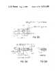
- FIGS. 7A-7CThe details of the latch foot 605 are shown in FIGS. 7A-7C, the latch spring 603 is shown in FIGS. 8A-8C, and an assembled latch spring 603 and latch foot 605 is shown in FIGS. 9A and 9B.
- the details of the latch nut 609are shown in FIGS. 10A-10C; the details of the latch cylinder 615 are shown in FIG. 11; the details of the support 618 are shown in FIGS. 12A-12C; the details of alignment lip 95 are shown in FIGS. 13A-13C; the details of door pull 617 are shown in FIGS. 14A-14C; and the details of port latch 613 are shown in FIGS. 15A-15C.
- a piston 230 of the elevator 70is located outside of spaces 10 and 90 to conserve space within the enclosures.
- Piston 230is coupled to door 60 by an arm 240 and rod 250.
- the rod 250passes through the wall of space 10 by means of a bellows 260 which prevents the intrusion of dirty ambient air.
- a vent 270is provided to allow the equalization of air pressure inside of bellows 260 as the elevator 70 moves and the bellows 260 expands and contracts. Note that the air passing through vent 270 is dirty ambient air, but this does not contaminate space 10 because the bellows is sealed to the inside of space 10 and arm 250.
- latches 210are released, piston 230 is extended, and the elevator 70 transports both doors 60 and 100 as a unit into space 10, thereby carrying the cassette 80 aligned with the aid of guide lips 275 into space 10 while trapping surface particles between the two doors 60 and 100 and preventing the intrusion of dirty ambient air.
- the doors 60 and 100need not fit flush with each other along the entire interface 110. In fact, it is desirable that an air gap 290 inside of the outer perimeters 280 and 285 be left between the doors 60 and 100.
- the air gap 290provides a compressive air space between the doors 60 and 100 so that the dirty air trapped between the doors 60 and 100 does not rush out at high velocity in the plane perpendicular to axis 200 as the doors 60 and 100 are brought together, thereby potentially sweeping part of the dirty trapped air into spaced 10 or 90.
- the air gap 290also prevents doors 60 and 100 from becoming affixed together by air pressure as could occur if the contact area 190 was a large, closely fitting surface. Typically the air gap 290 will occupy more than 80% of the contact opening 195.
- the doors 60 and 100should fit together so that perimeters 280 and 285 form one continuous surface. Therefore, joggle 295 where perimeters 280 and 285 meet should be kept as small as possible (e.g., less than 0.010-0.020 inch) since particles on the joggle 295 will be brought within the clean spaces 10 and 90 when the interface 110 is opened. Some particles may be present on the perimeters 280 and 285 so a particle gutter 297 is provided on door 60 to catch any particles which might roll down the perimeters 280 and 285 when the interface 110 is opened. Alternatively, particle gutter 297 can be omitted to permit any particles from the perimeters 280 and 285 to settle all the way to the bottom of the canopy 10.
- FIG. 16shows a SMIF box storage unit 300.
- the box storage unit 300is basically an open rack for storing cassette boxes 90.
- FIG. 17shows a cassette storage unit 320 for storing cassettes 80 holding IC wafers.
- the cassette storage unit 320is a desiccator box with a canopy 10, port 20, and manipulator 30 added to it.
- the cassette storage unit 320will typically function as a cassette processing buffer.
- Initial cassette entry into the SMIF systemoccurs through the system interlock 330 as shown in FIG. 18. This is typically a four-foot wide glove box with an access chamber 340 at one end and a SMIF port 20 at the other end.
- the complex movements required to transfer wafers from a new wafer package 345 into a cassette (not shown)necessitates the use of gloves 350 rather than mechanisms.
- Cassettes 80 and wafersenter and leave the SMIF system through the access chamber 340.
- the air filtration unit 355can contain both a conventional forced air filter and/or a particle collector such as an electrostatic precipitator.
- a particle collectorsuch as an electrostatic precipitator.
- gloves 350could be used to provide further flexibility of motion within canopy 10. Such gloves 350 are especially useful to provide maintenance within canopy 10 during periods when no IC wafers are present which can be contaminated by the intrusion of outside unfiltered air caused by use of the gloves 350. Filtration units 355 could also be used on the canopy 10 during such maintenance periods to remove any particles which may have intruded.
- ICsare transported in their own closed containers and handling is done primarily by mechanical arms it is also possible to automate the IC production facility by the use of stationary or mobile robots which use computer controlled robotic manipulators coupled to the SMIF components. Whether handling is done manually or automatically, by combining the SMIF components with conventional IC processing equipment the IC fabrication area can for the first time be constructed without the need of a conventional clean room environment, while at the same time improving IC cleanliness.
Landscapes
- Engineering & Computer Science (AREA)
- Physics & Mathematics (AREA)
- Condensed Matter Physics & Semiconductors (AREA)
- General Physics & Mathematics (AREA)
- Manufacturing & Machinery (AREA)
- Computer Hardware Design (AREA)
- Microelectronics & Electronic Packaging (AREA)
- Power Engineering (AREA)
- Container, Conveyance, Adherence, Positioning, Of Wafer (AREA)
Abstract
Description
Claims (8)
Priority Applications (4)
| Application Number | Priority Date | Filing Date | Title |
|---|---|---|---|
| US06/594,498US4534389A (en) | 1984-03-29 | 1984-03-29 | Interlocking door latch for dockable interface for integrated circuit processing |
| DE8484306602TDE3483828D1 (en) | 1983-09-28 | 1984-09-28 | PROCESSING SYSTEM FOR INTEGRATED CIRCUITS. |
| EP19840306602EP0151336B1 (en) | 1983-09-28 | 1984-09-28 | System for integrated circuit processing |
| JP60064936AJPS60220945A (en) | 1984-03-29 | 1985-03-28 | Treatment apparatus for integrated circuit |
Applications Claiming Priority (1)
| Application Number | Priority Date | Filing Date | Title |
|---|---|---|---|
| US06/594,498US4534389A (en) | 1984-03-29 | 1984-03-29 | Interlocking door latch for dockable interface for integrated circuit processing |
Publications (1)
| Publication Number | Publication Date |
|---|---|
| US4534389Atrue US4534389A (en) | 1985-08-13 |
Family
ID=24379124
Family Applications (1)
| Application Number | Title | Priority Date | Filing Date |
|---|---|---|---|
| US06/594,498Expired - LifetimeUS4534389A (en) | 1983-09-28 | 1984-03-29 | Interlocking door latch for dockable interface for integrated circuit processing |
Country Status (2)
| Country | Link |
|---|---|
| US (1) | US4534389A (en) |
| JP (1) | JPS60220945A (en) |
Cited By (96)
| Publication number | Priority date | Publication date | Assignee | Title |
|---|---|---|---|---|
| US4616683A (en)* | 1983-09-28 | 1986-10-14 | Hewlett-Packard Company | Particle-free dockable interface for integrated circuit processing |
| US4636128A (en)* | 1984-08-30 | 1987-01-13 | Texas Instruments Incorporated | Semiconductor slice cassette transport unit |
| WO1987001361A1 (en)* | 1985-08-26 | 1987-03-12 | Asyst Technologies | Manipulator for standard mechanical interface apparatus |
| US4668153A (en)* | 1984-11-07 | 1987-05-26 | British Nuclear Fuels | Apparatus for posting materials into and out of enclosures |
| US4674939A (en)* | 1984-07-30 | 1987-06-23 | Asyst Technologies | Sealed standard interface apparatus |
| US4705444A (en)* | 1985-07-24 | 1987-11-10 | Hewlett-Packard Company | Apparatus for automated cassette handling |
| US4724874A (en)* | 1986-05-01 | 1988-02-16 | Asyst Technologies | Sealable transportable container having a particle filtering system |
| US4739882A (en)* | 1986-02-13 | 1988-04-26 | Asyst Technologies | Container having disposable liners |
| US4815912A (en)* | 1984-12-24 | 1989-03-28 | Asyst Technologies, Inc. | Box door actuated retainer |
| US4895486A (en)* | 1987-05-15 | 1990-01-23 | Roboptek, Inc. | Wafer monitoring device |
| US4901011A (en)* | 1988-11-04 | 1990-02-13 | Tokyo Electron Limited | Carrier for transferring plate-like objects one by one, a handling apparatus for loading or unloading the carrier, and a wafer probing machine fitted with the handling apparatus for the wafer carrier |
| US4924890A (en)* | 1986-05-16 | 1990-05-15 | Eastman Kodak Company | Method and apparatus for cleaning semiconductor wafers |
| US4963069A (en)* | 1986-11-06 | 1990-10-16 | Meissner & Wurst Gmbh & Co. | Container for the handling of semiconductor devices and process for particle-free transfer |
| WO1990014273A1 (en)* | 1989-05-19 | 1990-11-29 | Asyst Technologies, Inc. | Sealable transportable container having improved latch mechanism |
| US4976579A (en)* | 1988-04-21 | 1990-12-11 | British Nuclear Fuels Plc | Flask assembly for contaminated objects |
| US5056875A (en)* | 1989-03-20 | 1991-10-15 | Motorola, Inc. | Container for use within a clean environment |
| US5058491A (en)* | 1990-08-27 | 1991-10-22 | Taiwan Semiconductor Manufacturing Company, Ltd. | Building and method for manufacture of integrated circuits |
| WO1992007759A1 (en)* | 1990-11-01 | 1992-05-14 | Asyst Technologies, Inc. | Method and apparatus for transferring articles between two controlled environments |
| USRE34311E (en)* | 1984-08-30 | 1993-07-13 | Texas Instruments Incorporated | Semiconductor slice cassette transport unit |
| US5226781A (en)* | 1991-03-20 | 1993-07-13 | Euritech | Process and installation for transferring products from a contaminated enclosure into a second enclosure without contaminating the latter |
| US5256204A (en)* | 1991-12-13 | 1993-10-26 | United Microelectronics Corporation | Single semiconductor water transfer method and manufacturing system |
| US5277654A (en)* | 1992-10-08 | 1994-01-11 | John's Insulation, Inc. | Method and apparatus for protectively transporting contaminated personnel and the like |
| US5291923A (en)* | 1992-09-24 | 1994-03-08 | Internatinal Business Machines Corporation | Door opening system and method |
| US5291925A (en)* | 1991-09-18 | 1994-03-08 | Piero Marrucchi | Equipment for forming temporary connections for the transfer of objects between discontinuous confined volumes |
| US5339952A (en)* | 1992-06-19 | 1994-08-23 | International Business Machines Corporation | Transfer container for transferring flimsy circuit panels under clean room conditions |
| US5346518A (en)* | 1993-03-23 | 1994-09-13 | International Business Machines Corporation | Vapor drain system |
| US5350336A (en)* | 1993-04-23 | 1994-09-27 | Industrial Technology Research Institute | Building and method for manufacture of integrated semiconductor circuit devices |
| US5364225A (en)* | 1992-06-19 | 1994-11-15 | Ibm | Method of printed circuit panel manufacture |
| US5364219A (en)* | 1991-06-24 | 1994-11-15 | Tdk Corporation | Apparatus for clean transfer of objects |
| US5391035A (en)* | 1992-11-06 | 1995-02-21 | Applied Materials, Inc. | Micro-enviroment load lock |
| US5395198A (en)* | 1992-06-19 | 1995-03-07 | International Business Machines Corporation | Vacuum loading chuck and fixture for flexible printed circuit panels |
| US5433574A (en)* | 1992-05-21 | 1995-07-18 | Shinko Electric Co., Ltd. | Gas purge unit for a portable container |
| US5451131A (en)* | 1992-06-19 | 1995-09-19 | International Business Machines Corporation | Dockable interface airlock between process enclosure and interprocess transfer container |
| EP0684631A1 (en)* | 1994-05-24 | 1995-11-29 | Fluoroware, Inc. | Standardized mechanical interface (SMIF) pod. |
| US5476176A (en)* | 1994-05-23 | 1995-12-19 | Empak, Inc. | Reinforced semiconductor wafer holder |
| US5538390A (en)* | 1993-10-29 | 1996-07-23 | Applied Materials, Inc. | Enclosure for load lock interface |
| US5570987A (en)* | 1993-12-14 | 1996-11-05 | W. L. Gore & Associates, Inc. | Semiconductor wafer transport container |
| USD376688S (en) | 1994-12-20 | 1996-12-24 | Empak, Inc. | Semiconductor wafer cassette transport box |
| US5668056A (en)* | 1990-12-17 | 1997-09-16 | United Microelectronics Corporation | Single semiconductor wafer transfer method and manufacturing system |
| US5674039A (en)* | 1996-07-12 | 1997-10-07 | Fusion Systems Corporation | System for transferring articles between controlled environments |
| US5711427A (en)* | 1996-07-12 | 1998-01-27 | Fluoroware, Inc. | Wafer carrier with door |
| US5713711A (en)* | 1995-01-17 | 1998-02-03 | Bye/Oasis | Multiple interface door for wafer storage and handling container |
| US5730573A (en)* | 1994-02-22 | 1998-03-24 | Tdk Corporation | Clean transfer method and apparatus therefor |
| US5740053A (en)* | 1995-07-31 | 1998-04-14 | Tokyo Electron Limited | Method of controlling monitor used in cleaning machine and object processing machine and monitor apparatus |
| US5752796A (en)* | 1996-01-24 | 1998-05-19 | Muka; Richard S. | Vacuum integrated SMIF system |
| US5788082A (en)* | 1996-07-12 | 1998-08-04 | Fluoroware, Inc. | Wafer carrier |
| WO1998046503A1 (en) | 1997-04-14 | 1998-10-22 | Asyst Technologies, Inc. | Integrated intrabay buffer, delivery, and stocker system |
| US5833726A (en)* | 1995-05-26 | 1998-11-10 | Extraction System, Inc. | Storing substrates between process steps within a processing facility |
| US5915562A (en)* | 1996-07-12 | 1999-06-29 | Fluoroware, Inc. | Transport module with latching door |
| US5944475A (en)* | 1996-10-11 | 1999-08-31 | Asyst Technologies, Inc. | Rotated, orthogonal load compatible front-opening interface |
| WO1999047864A1 (en) | 1998-03-16 | 1999-09-23 | Asyst Technologies, Inc. | Intelligent minienvironment |
| WO1999050577A1 (en)* | 1998-03-27 | 1999-10-07 | Asyst Technologies, Inc. | Kinematic coupling compatible, passive interface seal |
| US6045620A (en)* | 1997-07-11 | 2000-04-04 | Applied Materials, Inc. | Two-piece slit valve insert for vacuum processing system |
| WO2000032472A1 (en) | 1998-12-01 | 2000-06-08 | Asyst Technologies, Inc. | Passively activated valve for carrier purging |
| US6120229A (en)* | 1999-02-01 | 2000-09-19 | Brooks Automation Inc. | Substrate carrier as batchloader |
| US6135698A (en)* | 1999-04-30 | 2000-10-24 | Asyst Technologies, Inc. | Universal tool interface and/or workpiece transfer apparatus for SMIF and open pod applications |
| US6157866A (en)* | 1997-06-19 | 2000-12-05 | Advanced Micro Devices, Inc. | Automated material handling system for a manufacturing facility divided into separate fabrication areas |
| US6188323B1 (en)* | 1998-10-15 | 2001-02-13 | Asyst Technologies, Inc. | Wafer mapping system |
| US6319297B1 (en)* | 1998-03-27 | 2001-11-20 | Asyst Technologies, Inc. | Modular SMIF pod breather, adsorbent, and purge cartridges |
| US20020020751A1 (en)* | 2000-08-04 | 2002-02-21 | Ken Matsumoto | Substrate transfer apparatus, semiconductor manufacturing apparatus, and semiconductor device manufacturing method |
| US6352403B1 (en) | 1992-11-06 | 2002-03-05 | Applied Materials, Inc. | Controlled environment enclosure and mechanical interface |
| US6364595B1 (en) | 1999-02-10 | 2002-04-02 | Asyst Technologies, Inc. | Reticle transfer system |
| US6419438B1 (en) | 2000-11-28 | 2002-07-16 | Asyst Technologies, Inc. | FIMS interface without alignment pins |
| WO2002056344A2 (en) | 2001-01-10 | 2002-07-18 | Entegris Cayman Ltd. | Transportable container including an internal environment monitor |
| WO2002062681A1 (en)* | 2001-02-02 | 2002-08-15 | Asyst Technologies, Inc. | System for safeguarding integrated intrabay pod delivery and storage system |
| US6471037B1 (en) | 1999-09-01 | 2002-10-29 | Canon Kabushiki Kaisha | Semiconductor manufacturing apparatus and method |
| US6502869B1 (en)* | 1998-07-14 | 2003-01-07 | Asyst Technologies, Inc. | Pod door to port door retention system |
| US6517304B1 (en) | 1999-03-31 | 2003-02-11 | Canon Kabushiki Kaisha | Method for transporting substrates and a semiconductor manufacturing apparatus using the method |
| US6520727B1 (en) | 2000-04-12 | 2003-02-18 | Asyt Technologies, Inc. | Modular sorter |
| US6536813B2 (en)* | 2000-07-10 | 2003-03-25 | Asyst Technologies, Inc. | SMIF container latch mechanism |
| US6591162B1 (en) | 2000-08-15 | 2003-07-08 | Asyst Technologies, Inc. | Smart load port with integrated carrier monitoring and fab-wide carrier management system |
| US6623051B2 (en) | 2000-12-13 | 2003-09-23 | Entegris, Inc. | Laterally floating latch hub assembly |
| US6663148B2 (en) | 2000-12-13 | 2003-12-16 | Entegris, Inc. | System for preventing improper insertion of FOUP door into FOUP |
| US6679672B1 (en)* | 2003-03-10 | 2004-01-20 | Syracuse University | Transfer port for movement of materials between clean rooms |
| US20040026694A1 (en)* | 2000-07-09 | 2004-02-12 | Jakob Blattner | Storage device, especially for the intermediate storage of test wafers |
| US6776289B1 (en) | 1996-07-12 | 2004-08-17 | Entegris, Inc. | Wafer container with minimal contact |
| US6811369B2 (en) | 1999-09-02 | 2004-11-02 | Canon Kabushiki Kaisha | Semiconductor fabrication apparatus, pod carry apparatus, pod carry method, and semiconductor device production method |
| US20050109668A1 (en)* | 2003-10-24 | 2005-05-26 | John Burns | Substrate carrier |
| US20060061979A1 (en)* | 2004-09-04 | 2006-03-23 | Applied Materials, Inc. | Substrate carrier having reduced height |
| US20060076264A1 (en)* | 2004-10-07 | 2006-04-13 | Cletuswittman Boyd | Reticle carrier |
| US20070116545A1 (en)* | 2005-11-21 | 2007-05-24 | Applied Materials, Inc. | Apparatus and methods for a substrate carrier having an inflatable seal |
| US20070141280A1 (en)* | 2005-12-16 | 2007-06-21 | Applied Materials, Inc. | Substrate carrier having an interior lining |
| DE19882568B4 (en)* | 1997-08-01 | 2008-02-21 | Entegris, Inc., Chaska | Container for semiconductor wafers |
| CN100418700C (en)* | 2003-10-02 | 2008-09-17 | 台湾积体电路制造股份有限公司 | Manufacturing system, distribution system, and distribution method |
| US20080302700A1 (en)* | 1997-07-11 | 2008-12-11 | Nyseth David L | Transport module |
| US20090053017A1 (en)* | 2006-03-17 | 2009-02-26 | Shlomo Shmuelov | Storage and purge system for semiconductor wafers |
| US20090056116A1 (en)* | 2007-08-07 | 2009-03-05 | Micro Foundry Inc. | Integrated miniature device factory |
| US20100126904A1 (en)* | 2008-11-21 | 2010-05-27 | Kung-Hao Cheng | Thin-plate container |
| US20100163452A1 (en)* | 2008-12-26 | 2010-07-01 | Chin-Ming Lin | Wafer container having the purging valve |
| US20120247671A1 (en)* | 2011-03-31 | 2012-10-04 | Tokyo Electron Limited | Substrate processing apparatus |
| US20120267363A1 (en)* | 2011-04-22 | 2012-10-25 | Askey Computer Corporation | Insulation Box Having Two Boards and a Spring Disposed Between the Boards |
| WO2013049178A2 (en) | 2011-09-27 | 2013-04-04 | The Board Of Regents Of The University Of Texas System | Robotic infusion mixer and transportable cartridge |
| US8950624B2 (en) | 2011-12-29 | 2015-02-10 | Giuseppe Sacca | Externally operated alpha port system for use with a rapid transfer port |
| US10062591B2 (en)* | 2013-08-01 | 2018-08-28 | Shanghai Ic R&D Center Co., Ltd | Equipment platform system and wafer transfer method thereof |
| US20190041756A1 (en)* | 2008-09-29 | 2019-02-07 | Tokyo Electron Limited | Mask pattern forming method, fine pattern forming method, and film deposition apparatus |
| DE102020124826A1 (en) | 2020-09-23 | 2022-03-24 | Syntegon Technology Gmbh | Beta component of a transfer system for a sterile isolation area, sterile isolation area, aseptic filling system and a method for operating such a filling system |
Citations (8)
| Publication number | Priority date | Publication date | Assignee | Title |
|---|---|---|---|---|
| GB938311A (en)* | 1960-11-17 | 1963-10-02 | Commissariat Energie Atomique | Device for the removal of dangerous products |
| US3260381A (en)* | 1964-04-29 | 1966-07-12 | Robert N Wagner | Apparatus and method for transferring objects into a conditioned atmosphere |
| US3294670A (en)* | 1963-10-07 | 1966-12-27 | Western Electric Co | Apparatus for processing materials in a controlled atmosphere |
| US4047624A (en)* | 1975-10-21 | 1977-09-13 | Airco, Inc. | Workpiece handling system for vacuum processing |
| US4089341A (en)* | 1975-01-08 | 1978-05-16 | G. Kendall Parmelee | Connector method and apparatus for coupling two systems together while excluding the environment from the system interiors |
| US4201310A (en)* | 1978-02-24 | 1980-05-06 | La Calhene | Bidirectional joining device |
| US4260312A (en)* | 1978-09-27 | 1981-04-07 | United Kingdom Atomic Energy Authority | Apparatus for transferring toxic and radioactive materials |
| US4281691A (en)* | 1978-08-25 | 1981-08-04 | Commissariat A L'energie Atomique | Device for transferring and packaging contaminants such as radioactive products within a leak-tight sheath |
Family Cites Families (2)
| Publication number | Priority date | Publication date | Assignee | Title |
|---|---|---|---|---|
| JPS52127076A (en)* | 1976-04-17 | 1977-10-25 | Senken Kk | Container for carrying ic wafer |
| US4532970A (en)* | 1983-09-28 | 1985-08-06 | Hewlett-Packard Company | Particle-free dockable interface for integrated circuit processing |
- 1984
- 1984-03-29USUS06/594,498patent/US4534389A/ennot_activeExpired - Lifetime
- 1985
- 1985-03-28JPJP60064936Apatent/JPS60220945A/enactiveGranted
Patent Citations (8)
| Publication number | Priority date | Publication date | Assignee | Title |
|---|---|---|---|---|
| GB938311A (en)* | 1960-11-17 | 1963-10-02 | Commissariat Energie Atomique | Device for the removal of dangerous products |
| US3294670A (en)* | 1963-10-07 | 1966-12-27 | Western Electric Co | Apparatus for processing materials in a controlled atmosphere |
| US3260381A (en)* | 1964-04-29 | 1966-07-12 | Robert N Wagner | Apparatus and method for transferring objects into a conditioned atmosphere |
| US4089341A (en)* | 1975-01-08 | 1978-05-16 | G. Kendall Parmelee | Connector method and apparatus for coupling two systems together while excluding the environment from the system interiors |
| US4047624A (en)* | 1975-10-21 | 1977-09-13 | Airco, Inc. | Workpiece handling system for vacuum processing |
| US4201310A (en)* | 1978-02-24 | 1980-05-06 | La Calhene | Bidirectional joining device |
| US4281691A (en)* | 1978-08-25 | 1981-08-04 | Commissariat A L'energie Atomique | Device for transferring and packaging contaminants such as radioactive products within a leak-tight sheath |
| US4260312A (en)* | 1978-09-27 | 1981-04-07 | United Kingdom Atomic Energy Authority | Apparatus for transferring toxic and radioactive materials |
Cited By (135)
| Publication number | Priority date | Publication date | Assignee | Title |
|---|---|---|---|---|
| US4616683A (en)* | 1983-09-28 | 1986-10-14 | Hewlett-Packard Company | Particle-free dockable interface for integrated circuit processing |
| US4674939A (en)* | 1984-07-30 | 1987-06-23 | Asyst Technologies | Sealed standard interface apparatus |
| US4636128A (en)* | 1984-08-30 | 1987-01-13 | Texas Instruments Incorporated | Semiconductor slice cassette transport unit |
| USRE34311E (en)* | 1984-08-30 | 1993-07-13 | Texas Instruments Incorporated | Semiconductor slice cassette transport unit |
| US4668153A (en)* | 1984-11-07 | 1987-05-26 | British Nuclear Fuels | Apparatus for posting materials into and out of enclosures |
| US4815912A (en)* | 1984-12-24 | 1989-03-28 | Asyst Technologies, Inc. | Box door actuated retainer |
| US4705444A (en)* | 1985-07-24 | 1987-11-10 | Hewlett-Packard Company | Apparatus for automated cassette handling |
| WO1987001361A1 (en)* | 1985-08-26 | 1987-03-12 | Asyst Technologies | Manipulator for standard mechanical interface apparatus |
| US4739882A (en)* | 1986-02-13 | 1988-04-26 | Asyst Technologies | Container having disposable liners |
| US4724874A (en)* | 1986-05-01 | 1988-02-16 | Asyst Technologies | Sealable transportable container having a particle filtering system |
| US4924890A (en)* | 1986-05-16 | 1990-05-15 | Eastman Kodak Company | Method and apparatus for cleaning semiconductor wafers |
| US4963069A (en)* | 1986-11-06 | 1990-10-16 | Meissner & Wurst Gmbh & Co. | Container for the handling of semiconductor devices and process for particle-free transfer |
| US4895486A (en)* | 1987-05-15 | 1990-01-23 | Roboptek, Inc. | Wafer monitoring device |
| US4976579A (en)* | 1988-04-21 | 1990-12-11 | British Nuclear Fuels Plc | Flask assembly for contaminated objects |
| US4901011A (en)* | 1988-11-04 | 1990-02-13 | Tokyo Electron Limited | Carrier for transferring plate-like objects one by one, a handling apparatus for loading or unloading the carrier, and a wafer probing machine fitted with the handling apparatus for the wafer carrier |
| US5056875A (en)* | 1989-03-20 | 1991-10-15 | Motorola, Inc. | Container for use within a clean environment |
| US4995430A (en)* | 1989-05-19 | 1991-02-26 | Asyst Technologies, Inc. | Sealable transportable container having improved latch mechanism |
| WO1990014273A1 (en)* | 1989-05-19 | 1990-11-29 | Asyst Technologies, Inc. | Sealable transportable container having improved latch mechanism |
| US5058491A (en)* | 1990-08-27 | 1991-10-22 | Taiwan Semiconductor Manufacturing Company, Ltd. | Building and method for manufacture of integrated circuits |
| WO1992007759A1 (en)* | 1990-11-01 | 1992-05-14 | Asyst Technologies, Inc. | Method and apparatus for transferring articles between two controlled environments |
| US5169272A (en)* | 1990-11-01 | 1992-12-08 | Asyst Technologies, Inc. | Method and apparatus for transferring articles between two controlled environments |
| US5370491A (en)* | 1990-11-01 | 1994-12-06 | Asyst Technologies, Inc. | Method and apparatus for transferring articles between two controlled environments |
| US5547328A (en)* | 1990-11-01 | 1996-08-20 | Asyst Technologies, Inc. | Method and apparatus for transferring articles between two controlled environments |
| US5668056A (en)* | 1990-12-17 | 1997-09-16 | United Microelectronics Corporation | Single semiconductor wafer transfer method and manufacturing system |
| US5976199A (en)* | 1990-12-17 | 1999-11-02 | United Microelectronics Corp. | Single semiconductor wafer transfer method and manufacturing system |
| US5226781A (en)* | 1991-03-20 | 1993-07-13 | Euritech | Process and installation for transferring products from a contaminated enclosure into a second enclosure without contaminating the latter |
| US5364219A (en)* | 1991-06-24 | 1994-11-15 | Tdk Corporation | Apparatus for clean transfer of objects |
| US5291925A (en)* | 1991-09-18 | 1994-03-08 | Piero Marrucchi | Equipment for forming temporary connections for the transfer of objects between discontinuous confined volumes |
| US5256204A (en)* | 1991-12-13 | 1993-10-26 | United Microelectronics Corporation | Single semiconductor water transfer method and manufacturing system |
| US5372471A (en)* | 1991-12-13 | 1994-12-13 | United Microelectronics Corporation | Single semiconductor wafer transfer method and manufacturing system |
| US5433574A (en)* | 1992-05-21 | 1995-07-18 | Shinko Electric Co., Ltd. | Gas purge unit for a portable container |
| US5395198A (en)* | 1992-06-19 | 1995-03-07 | International Business Machines Corporation | Vacuum loading chuck and fixture for flexible printed circuit panels |
| US5339952A (en)* | 1992-06-19 | 1994-08-23 | International Business Machines Corporation | Transfer container for transferring flimsy circuit panels under clean room conditions |
| US5364225A (en)* | 1992-06-19 | 1994-11-15 | Ibm | Method of printed circuit panel manufacture |
| US5451131A (en)* | 1992-06-19 | 1995-09-19 | International Business Machines Corporation | Dockable interface airlock between process enclosure and interprocess transfer container |
| EP0589812A1 (en)* | 1992-09-24 | 1994-03-30 | International Business Machines Corporation | Sealable container for contamination sensitive items |
| US5291923A (en)* | 1992-09-24 | 1994-03-08 | Internatinal Business Machines Corporation | Door opening system and method |
| US5277654A (en)* | 1992-10-08 | 1994-01-11 | John's Insulation, Inc. | Method and apparatus for protectively transporting contaminated personnel and the like |
| US6352403B1 (en) | 1992-11-06 | 2002-03-05 | Applied Materials, Inc. | Controlled environment enclosure and mechanical interface |
| US5391035A (en)* | 1992-11-06 | 1995-02-21 | Applied Materials, Inc. | Micro-enviroment load lock |
| US5346518A (en)* | 1993-03-23 | 1994-09-13 | International Business Machines Corporation | Vapor drain system |
| US5350336A (en)* | 1993-04-23 | 1994-09-27 | Industrial Technology Research Institute | Building and method for manufacture of integrated semiconductor circuit devices |
| US5630690A (en)* | 1993-10-29 | 1997-05-20 | Applied Materials, Inc. | Enclosure for load lock interface |
| US5538390A (en)* | 1993-10-29 | 1996-07-23 | Applied Materials, Inc. | Enclosure for load lock interface |
| US5570987A (en)* | 1993-12-14 | 1996-11-05 | W. L. Gore & Associates, Inc. | Semiconductor wafer transport container |
| US5730573A (en)* | 1994-02-22 | 1998-03-24 | Tdk Corporation | Clean transfer method and apparatus therefor |
| US6062808A (en)* | 1994-02-22 | 2000-05-16 | Tdk Corporation | Clean transfer method and apparatus therefor |
| US5476176A (en)* | 1994-05-23 | 1995-12-19 | Empak, Inc. | Reinforced semiconductor wafer holder |
| EP0684631A1 (en)* | 1994-05-24 | 1995-11-29 | Fluoroware, Inc. | Standardized mechanical interface (SMIF) pod. |
| US5482161A (en)* | 1994-05-24 | 1996-01-09 | Fluoroware, Inc. | Mechanical interface wafer container |
| USD376688S (en) | 1994-12-20 | 1996-12-24 | Empak, Inc. | Semiconductor wafer cassette transport box |
| US5713711A (en)* | 1995-01-17 | 1998-02-03 | Bye/Oasis | Multiple interface door for wafer storage and handling container |
| US5833726A (en)* | 1995-05-26 | 1998-11-10 | Extraction System, Inc. | Storing substrates between process steps within a processing facility |
| US5740053A (en)* | 1995-07-31 | 1998-04-14 | Tokyo Electron Limited | Method of controlling monitor used in cleaning machine and object processing machine and monitor apparatus |
| US5752796A (en)* | 1996-01-24 | 1998-05-19 | Muka; Richard S. | Vacuum integrated SMIF system |
| US5915562A (en)* | 1996-07-12 | 1999-06-29 | Fluoroware, Inc. | Transport module with latching door |
| US5788082A (en)* | 1996-07-12 | 1998-08-04 | Fluoroware, Inc. | Wafer carrier |
| US5711427A (en)* | 1996-07-12 | 1998-01-27 | Fluoroware, Inc. | Wafer carrier with door |
| US5674039A (en)* | 1996-07-12 | 1997-10-07 | Fusion Systems Corporation | System for transferring articles between controlled environments |
| US6776289B1 (en) | 1996-07-12 | 2004-08-17 | Entegris, Inc. | Wafer container with minimal contact |
| US5944475A (en)* | 1996-10-11 | 1999-08-31 | Asyst Technologies, Inc. | Rotated, orthogonal load compatible front-opening interface |
| WO1998046503A1 (en) | 1997-04-14 | 1998-10-22 | Asyst Technologies, Inc. | Integrated intrabay buffer, delivery, and stocker system |
| US7092779B1 (en) | 1997-06-19 | 2006-08-15 | Conboy Michael R | Automated material handling system for a manufacturing facility divided into separate fabrication areas |
| US6157866A (en)* | 1997-06-19 | 2000-12-05 | Advanced Micro Devices, Inc. | Automated material handling system for a manufacturing facility divided into separate fabrication areas |
| US20080302700A1 (en)* | 1997-07-11 | 2008-12-11 | Nyseth David L | Transport module |
| US6045620A (en)* | 1997-07-11 | 2000-04-04 | Applied Materials, Inc. | Two-piece slit valve insert for vacuum processing system |
| DE19882568B4 (en)* | 1997-08-01 | 2008-02-21 | Entegris, Inc., Chaska | Container for semiconductor wafers |
| WO1999047864A1 (en) | 1998-03-16 | 1999-09-23 | Asyst Technologies, Inc. | Intelligent minienvironment |
| USRE39241E1 (en)* | 1998-03-27 | 2006-08-22 | Entegris, Inc. | Modular SMIF pod breather, adsorbent, and purge cartridges |
| US6319297B1 (en)* | 1998-03-27 | 2001-11-20 | Asyst Technologies, Inc. | Modular SMIF pod breather, adsorbent, and purge cartridges |
| US6164664A (en)* | 1998-03-27 | 2000-12-26 | Asyst Technologies, Inc. | Kinematic coupling compatible passive interface seal |
| WO1999050577A1 (en)* | 1998-03-27 | 1999-10-07 | Asyst Technologies, Inc. | Kinematic coupling compatible, passive interface seal |
| US6502869B1 (en)* | 1998-07-14 | 2003-01-07 | Asyst Technologies, Inc. | Pod door to port door retention system |
| US6188323B1 (en)* | 1998-10-15 | 2001-02-13 | Asyst Technologies, Inc. | Wafer mapping system |
| WO2000032472A1 (en) | 1998-12-01 | 2000-06-08 | Asyst Technologies, Inc. | Passively activated valve for carrier purging |
| CN1117010C (en)* | 1998-12-01 | 2003-08-06 | 阿西斯特技术公司 | Passively activated valve for carrier purging |
| US6120229A (en)* | 1999-02-01 | 2000-09-19 | Brooks Automation Inc. | Substrate carrier as batchloader |
| US6364595B1 (en) | 1999-02-10 | 2002-04-02 | Asyst Technologies, Inc. | Reticle transfer system |
| US6517304B1 (en) | 1999-03-31 | 2003-02-11 | Canon Kabushiki Kaisha | Method for transporting substrates and a semiconductor manufacturing apparatus using the method |
| US6135698A (en)* | 1999-04-30 | 2000-10-24 | Asyst Technologies, Inc. | Universal tool interface and/or workpiece transfer apparatus for SMIF and open pod applications |
| CN1294658C (en)* | 1999-04-30 | 2007-01-10 | 阿西斯特技术公司 | Universal tool interface and/or workpiece transfer apparatus for SMIF and open pod applications |
| WO2000067334A1 (en)* | 1999-04-30 | 2000-11-09 | Asyst Technologies, Inc. | Universal tool interface and/or workpiece transfer apparatus for smif and open pod applications |
| US6471037B1 (en) | 1999-09-01 | 2002-10-29 | Canon Kabushiki Kaisha | Semiconductor manufacturing apparatus and method |
| US6759334B2 (en) | 1999-09-01 | 2004-07-06 | Canon Kabushiki Kaisha | Semiconductor manufacturing apparatus and method |
| US6811369B2 (en) | 1999-09-02 | 2004-11-02 | Canon Kabushiki Kaisha | Semiconductor fabrication apparatus, pod carry apparatus, pod carry method, and semiconductor device production method |
| US6520727B1 (en) | 2000-04-12 | 2003-02-18 | Asyt Technologies, Inc. | Modular sorter |
| US20040026694A1 (en)* | 2000-07-09 | 2004-02-12 | Jakob Blattner | Storage device, especially for the intermediate storage of test wafers |
| US6536813B2 (en)* | 2000-07-10 | 2003-03-25 | Asyst Technologies, Inc. | SMIF container latch mechanism |
| EP1412600A4 (en)* | 2000-07-10 | 2005-09-14 | Asyst Technologies | Smif container latch mechanism |
| US7147166B2 (en) | 2000-08-04 | 2006-12-12 | Canon Kabushiki Kaisha | Substrate transfer apparatus, semiconductor manufacturing apparatus, and semiconductor device manufacturing method |
| US20020020751A1 (en)* | 2000-08-04 | 2002-02-21 | Ken Matsumoto | Substrate transfer apparatus, semiconductor manufacturing apparatus, and semiconductor device manufacturing method |
| US6591162B1 (en) | 2000-08-15 | 2003-07-08 | Asyst Technologies, Inc. | Smart load port with integrated carrier monitoring and fab-wide carrier management system |
| US6419438B1 (en) | 2000-11-28 | 2002-07-16 | Asyst Technologies, Inc. | FIMS interface without alignment pins |
| US6663148B2 (en) | 2000-12-13 | 2003-12-16 | Entegris, Inc. | System for preventing improper insertion of FOUP door into FOUP |
| US6623051B2 (en) | 2000-12-13 | 2003-09-23 | Entegris, Inc. | Laterally floating latch hub assembly |
| US7156129B2 (en) | 2001-01-10 | 2007-01-02 | Entegris, Inc. | Transportable container including an internal environment monitor |
| US20050284535A1 (en)* | 2001-01-10 | 2005-12-29 | Entegris, Inc. | Transportable container including an internal environment monitor |
| US20070185687A1 (en)* | 2001-01-10 | 2007-08-09 | Entegris, Inc. | Transportable container including an internal environment monitor |
| US7490637B2 (en) | 2001-01-10 | 2009-02-17 | Entegris, Inc. | Transportable container including an internal environment monitor |
| WO2002056344A2 (en) | 2001-01-10 | 2002-07-18 | Entegris Cayman Ltd. | Transportable container including an internal environment monitor |
| US6901971B2 (en) | 2001-01-10 | 2005-06-07 | Entegris, Inc. | Transportable container including an internal environment monitor |
| US6677690B2 (en) | 2001-02-02 | 2004-01-13 | Asyst Technologies, Inc. | System for safeguarding integrated intrabay pod delivery and storage system |
| WO2002062681A1 (en)* | 2001-02-02 | 2002-08-15 | Asyst Technologies, Inc. | System for safeguarding integrated intrabay pod delivery and storage system |
| US6679672B1 (en)* | 2003-03-10 | 2004-01-20 | Syracuse University | Transfer port for movement of materials between clean rooms |
| CN100418700C (en)* | 2003-10-02 | 2008-09-17 | 台湾积体电路制造股份有限公司 | Manufacturing system, distribution system, and distribution method |
| US20050109668A1 (en)* | 2003-10-24 | 2005-05-26 | John Burns | Substrate carrier |
| US7347329B2 (en) | 2003-10-24 | 2008-03-25 | Entegris, Inc. | Substrate carrier |
| US20070057322A1 (en)* | 2004-09-04 | 2007-03-15 | Applied Materials, Inc. | Substrate carrier having reduced height |
| US20060061979A1 (en)* | 2004-09-04 | 2006-03-23 | Applied Materials, Inc. | Substrate carrier having reduced height |
| US7380668B2 (en) | 2004-10-07 | 2008-06-03 | Fab Integrated Technology, Inc. | Reticle carrier |
| US20060076264A1 (en)* | 2004-10-07 | 2006-04-13 | Cletuswittman Boyd | Reticle carrier |
| US20070116545A1 (en)* | 2005-11-21 | 2007-05-24 | Applied Materials, Inc. | Apparatus and methods for a substrate carrier having an inflatable seal |
| US20070141280A1 (en)* | 2005-12-16 | 2007-06-21 | Applied Materials, Inc. | Substrate carrier having an interior lining |
| US20090053017A1 (en)* | 2006-03-17 | 2009-02-26 | Shlomo Shmuelov | Storage and purge system for semiconductor wafers |
| US20090056116A1 (en)* | 2007-08-07 | 2009-03-05 | Micro Foundry Inc. | Integrated miniature device factory |
| US20190041756A1 (en)* | 2008-09-29 | 2019-02-07 | Tokyo Electron Limited | Mask pattern forming method, fine pattern forming method, and film deposition apparatus |
| US12288671B2 (en) | 2008-09-29 | 2025-04-29 | Tokyo Electron Limited | Film deposition apparatus for fine pattern forming |
| US11881379B2 (en) | 2008-09-29 | 2024-01-23 | Tokyo Electron Limited | Film deposition apparatus for fine pattern forming |
| US11404271B2 (en) | 2008-09-29 | 2022-08-02 | Tokyo Electron Limited | Film deposition apparatus for fine pattern forming |
| US11404272B2 (en) | 2008-09-29 | 2022-08-02 | Tokyo Electron Limited | Film deposition apparatus for fine pattern forming |
| US10879066B2 (en)* | 2008-09-29 | 2020-12-29 | Tokyo Electron Limited | Mask pattern forming method, fine pattern forming method, and film deposition apparatus |
| US20100126904A1 (en)* | 2008-11-21 | 2010-05-27 | Kung-Hao Cheng | Thin-plate container |
| US20100163452A1 (en)* | 2008-12-26 | 2010-07-01 | Chin-Ming Lin | Wafer container having the purging valve |
| US7950524B2 (en) | 2008-12-26 | 2011-05-31 | Gudeng Precision Industrial Co., Ltd | Wafer container having the purging valve |
| US10224226B2 (en) | 2011-03-31 | 2019-03-05 | Tokyo Electron Limited | Substrate processing apparatus |
| US9799542B2 (en)* | 2011-03-31 | 2017-10-24 | Tokyo Electron Limited | Substrate processing apparatus |
| US11328910B2 (en) | 2011-03-31 | 2022-05-10 | Tokyo Electron Limited | Substrate processing apparatus |
| US20120247671A1 (en)* | 2011-03-31 | 2012-10-04 | Tokyo Electron Limited | Substrate processing apparatus |
| US20120267363A1 (en)* | 2011-04-22 | 2012-10-25 | Askey Computer Corporation | Insulation Box Having Two Boards and a Spring Disposed Between the Boards |
| WO2013049178A2 (en) | 2011-09-27 | 2013-04-04 | The Board Of Regents Of The University Of Texas System | Robotic infusion mixer and transportable cartridge |
| US8950624B2 (en) | 2011-12-29 | 2015-02-10 | Giuseppe Sacca | Externally operated alpha port system for use with a rapid transfer port |
| US10062591B2 (en)* | 2013-08-01 | 2018-08-28 | Shanghai Ic R&D Center Co., Ltd | Equipment platform system and wafer transfer method thereof |
| DE102020124826A1 (en) | 2020-09-23 | 2022-03-24 | Syntegon Technology Gmbh | Beta component of a transfer system for a sterile isolation area, sterile isolation area, aseptic filling system and a method for operating such a filling system |
| EP4217111A1 (en)* | 2020-09-23 | 2023-08-02 | Syntegon Technology GmbH | Beta component of a transfer system for a sterile isolation region, sterile isolation region, aseptic filling system, and method for operating such a filling system |
| EP4217111B1 (en)* | 2020-09-23 | 2025-07-23 | Syntegon Technology GmbH | Beta component of a transfer system for a sterile isolation area, sterile isolation area, aseptic filling equipment and method of operating such filling equipment |
Also Published As
| Publication number | Publication date |
|---|---|
| JPH0482057B2 (en) | 1992-12-25 |
| JPS60220945A (en) | 1985-11-05 |
Similar Documents
| Publication | Publication Date | Title |
|---|---|---|
| US4534389A (en) | Interlocking door latch for dockable interface for integrated circuit processing | |
| US4532970A (en) | Particle-free dockable interface for integrated circuit processing | |
| US4616683A (en) | Particle-free dockable interface for integrated circuit processing | |
| EP0138473A2 (en) | System for integrated circuit processing | |
| US5740845A (en) | Sealable, transportable container having a breather assembly | |
| US5752796A (en) | Vacuum integrated SMIF system | |
| US4995430A (en) | Sealable transportable container having improved latch mechanism | |
| US4815912A (en) | Box door actuated retainer | |
| US5451131A (en) | Dockable interface airlock between process enclosure and interprocess transfer container | |
| JP3324960B2 (en) | Article transfer system and method | |
| US5370491A (en) | Method and apparatus for transferring articles between two controlled environments | |
| US5431599A (en) | Environmental control system | |
| US5895191A (en) | Sealable, transportable container adapted for horizontal loading and unloading | |
| KR940002914B1 (en) | Apparatus for manufacturing semiconductor device | |
| US5810537A (en) | Isolation chamber transfer apparatus | |
| US5195922A (en) | Environmental control system | |
| EP0151336B1 (en) | System for integrated circuit processing | |
| TW201620065A (en) | Loading port and loading port atmoshpere substitution method | |
| WO1994017336A1 (en) | Environmental control system | |
| EP0288455B1 (en) | Box door actuated retainer | |
| US5364225A (en) | Method of printed circuit panel manufacture | |
| US5395198A (en) | Vacuum loading chuck and fixture for flexible printed circuit panels | |
| EP0574893A2 (en) | Method of printed circuit panel manufacture | |
| JPH1084034A (en) | Method for transferring and using semiconductor wafer carrier and its apparatus | |
| WO1999028965A1 (en) | Container and loader for substrate |
Legal Events
| Date | Code | Title | Description |
|---|---|---|---|
| AS | Assignment | Owner name:HEWLETT-PACKARD COMPANY PALO ALTO CALIFORNIA A COR Free format text:ASSIGNMENT OF ASSIGNORS INTEREST.;ASSIGNOR:TULLIS, BARCLAY J.;REEL/FRAME:004245/0274 Effective date:19840329 | |
| STCF | Information on status: patent grant | Free format text:PATENTED CASE | |
| FEPP | Fee payment procedure | Free format text:PAYOR NUMBER ASSIGNED (ORIGINAL EVENT CODE: ASPN); ENTITY STATUS OF PATENT OWNER: LARGE ENTITY | |
| FPAY | Fee payment | Year of fee payment:4 | |
| FPAY | Fee payment | Year of fee payment:8 | |
| FPAY | Fee payment | Year of fee payment:12 | |
| AS | Assignment | Owner name:HEWLETT-PACKARD COMPANY, A DELAWARE CORPORATION, C Free format text:MERGER;ASSIGNOR:HEWLETT-PACKARD COMPANY, A CALIFORNIA CORPORATION;REEL/FRAME:010841/0649 Effective date:19980520 | |
| AS | Assignment | Owner name:AGILENT TECHNOLOGIES INC., CALIFORNIA Free format text:ASSIGNMENT OF ASSIGNORS INTEREST;ASSIGNOR:HEWLETT-PACKARD COMPANY, A DELAWARE CORPORATION;REEL/FRAME:010901/0336 Effective date:20000520 | |
| AS | Assignment | Owner name:AVAGO TECHNOLOGIES GENERAL IP (SINGAPORE) PTE. LTD Free format text:ASSIGNMENT OF ASSIGNORS INTEREST;ASSIGNOR:AGILENT TECHNOLOGIES, INC.;REEL/FRAME:018367/0245 Effective date:20051201 |