US4532650A - Photomask inspection apparatus and method using corner comparator defect detection algorithm - Google Patents
Photomask inspection apparatus and method using corner comparator defect detection algorithmDownload PDFInfo
- Publication number
- US4532650A US4532650AUS06/494,762US49476283AUS4532650AUS 4532650 AUS4532650 AUS 4532650AUS 49476283 AUS49476283 AUS 49476283AUS 4532650 AUS4532650 AUS 4532650A
- Authority
- US
- United States
- Prior art keywords
- gradient
- signals
- matrix
- toggle
- corner
- Prior art date
- Legal status (The legal status is an assumption and is not a legal conclusion. Google has not performed a legal analysis and makes no representation as to the accuracy of the status listed.)
- Expired - Lifetime
Links
Images


Classifications
- G—PHYSICS
- G03—PHOTOGRAPHY; CINEMATOGRAPHY; ANALOGOUS TECHNIQUES USING WAVES OTHER THAN OPTICAL WAVES; ELECTROGRAPHY; HOLOGRAPHY
- G03F—PHOTOMECHANICAL PRODUCTION OF TEXTURED OR PATTERNED SURFACES, e.g. FOR PRINTING, FOR PROCESSING OF SEMICONDUCTOR DEVICES; MATERIALS THEREFOR; ORIGINALS THEREFOR; APPARATUS SPECIALLY ADAPTED THEREFOR
- G03F1/00—Originals for photomechanical production of textured or patterned surfaces, e.g., masks, photo-masks, reticles; Mask blanks or pellicles therefor; Containers specially adapted therefor; Preparation thereof
- G03F1/68—Preparation processes not covered by groups G03F1/20 - G03F1/50
- G03F1/82—Auxiliary processes, e.g. cleaning or inspecting
- G03F1/84—Inspecting
- G—PHYSICS
- G06—COMPUTING OR CALCULATING; COUNTING
- G06T—IMAGE DATA PROCESSING OR GENERATION, IN GENERAL
- G06T7/00—Image analysis
- G06T7/0002—Inspection of images, e.g. flaw detection
- G06T7/0004—Industrial image inspection
- G06T7/001—Industrial image inspection using an image reference approach
- G—PHYSICS
- G06—COMPUTING OR CALCULATING; COUNTING
- G06T—IMAGE DATA PROCESSING OR GENERATION, IN GENERAL
- G06T2207/00—Indexing scheme for image analysis or image enhancement
- G06T2207/30—Subject of image; Context of image processing
- G06T2207/30108—Industrial image inspection
- G06T2207/30148—Semiconductor; IC; Wafer
Definitions
- the present inventionrelates generally to object inspection apparatus and more particularly to an apparatus and method for inspecting photomasks having duplicate die patterns thereupon for defects by utilizing an edge and corner comparison defect detection technique to identify defects as differences between otherwise duplicate die patterns.
- die patternsmay be compared to corresponding data taken from a data base.
- a significant problem inherent in most prior art inspection systemsis that the efficiency of the defect detection circuitry is relatively poor for defects located near corners.
- some kind of template matching techniqueis usually employed.
- Another object of the present inventionis to provide an improved apparatus and method for quickly and efficiently detecting defects in duplicate die patterns of a photomask by aligning and comparing pixel representations of the die patterns in real time.
- a further object of the present inventionis to provide an electronic circuit for defect detection that concurrently processes pixel representations of die patterns using vector gradients within a matrix to detect edges and corners.
- Still another object of the present inventionis to provide a corner comparator defect detection apparatus and method having improved defect detection efficiency by reducing undetected and falsely detected defects.
- Still another object of the present inventionis to provide a defect detection apparatus and method that permits misalignment of plus or minus two pixels between pixel representations of duplicate die patterns without missing defects occuring near corners or producing false detections related thereto.
- An additional objective of the present inventionis to provide a defect detection apparatus and method using a corner comparison algorithm to maximize detection sensitivity to defects occuring at or near corners appearing in an image pattern.
- a preferred embodiment of the present inventionincludes a mechanical and optical system for scannning duplicate areas of a photomask to be inspected, electronic means for converting the optically scanned information to digitized form, means for storing such information, and means for comparing information obtained from one inspected area to the other inspected area to determine differences therebetween, such differences being classified as defects.
- the detectionis accomplished using a vector gradient within a matrix technique to develop candidate and cancellor information which is then logically manipulated to qualify the data obtained from each pixel matrix and then after qualification, is used to determine whether or not a defect has been detected.
- the subject inventionhas particular application to the detection of defects occuring at pattern corners within the inspected photomask and is specifically directed to overcoming difficulties previously encountered in detecting such defects.
- the present inventiondynamically detects errors occuring at or near corners even though the pixel representations used to effect the comparison may not be precisely aligned.
- Another advantage of the present inventionis that the defect detection circuit is particularly sensitive to defects occuring at or near pattern corners.
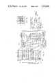
- FIG. 1is a functional block diagram showing a photomask inspection apparatus in accordance with the present invention for scanning, detecting and recording defects occuring in the patterns of a photomask;
- FIG. 2is a schematic showing in plan view of a photomask illustrating the simultaneous scanning of a pair of duplicate die patterns in accordance with the present invention
- FIG. 3is a diagram conceptually illustrating operation of the present invention
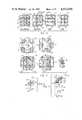
- FIGS. 4 and 4aare pixel matrix diagrams illustrating the gradient tests performed in accordance with the present invention.
- FIG. 5is an illustration depicting nine corner configurations detectable in accordance with the present invention.
- FIGS. 6 and 7are diagrams schematically illustrating a corner identification technique in accordance with the present invention.
- FIG. 8is a block diagram schematically illustrating the function components of the detection and signal qualifying logic used in implementing the present invention.
- FIG. 9is a logic diagram illustrating combinational logic used to process the signals developed by the logic shown in FIG. 8 of the drawing.
- FIG. 1 of the drawinga preferred embodiment of a photomask inspection system according to the present invention is schematically illustrated in general at 20.
- the systemincludes an air-bearing stage 22 mounted on a granite table 24 for transporting and positioning a photomask 26 to be inspected.
- Stage 22is movable in the X and Y directions (indicated by the arrows 28 and 30) by motors that are schematically illustrated at 32 and 34, respectively.
- a photomask holder 36is rotatable in the XY plane by a motor 38 to allow the photomask to be aligned with the X and Y reference directions.
- the photomask 26which will later be used to produce semi-conductor chip devices, typically on a circular wafer such as is illustrated at 27, is scanned in a raster pattern, as illustrated by the lines 29, with two accurately spaced viewing areas 31 and 33 being inspected simultaneously. Inspection for defects is accomplished by comparing pixel representations obtained from viewing areas 31 and 33 containing duplicate die patterns, and defects are identified at those locations in which the two pixel representations do not match.
- Pixel representationsare formed by a combination of optical and electronic means, the former including an illuminator 40 (FIG. 1) disposed beneath the granite table 24 and which illuminates the bottom of the photomask through an opening in table 24. Also included are left and right optical inspection systems 42 and 44, respectively, which project images of light transmitted through the transparent portions of the photomask onto a binocular viewhead 46 and onto left and right detectors 48 and 50, respectively.
- the binocular viewheadpermits viewing of a magnified image of the photomask by an operator.
- the task of focusing images of the photomask onto the left and right detectorsis performed by an automatic focus circuit 51 which responds to output signals generated by the detectors 48 and 50.
- the left and right inspection optic systems 42 and 44are positioned relative to each other so as to focus identical portions (areas 31 and 33 in FIG. 2) of two die patterns of photomask 56 onto the respective left and right detectors.
- the electronic means for forming pixel representations of the die patternsincludes the detectors 48 and 50 which generate analog voltage signals that are proportioned to the intensity of light impinging there upon, and left and right digitizers 52 and 54 which convert the analog voltage signals generated by the detectors into digital signals.
- the digital signalsare then stored temporarily in left and right pixel alignment memorys 56 and 58, respectively.
- the data input to the left pixel memorycould be taken via a switch 53 from a data base 55 which contains an electronically stored and known correct replica of the photomask being inspected.
- Memories 56 and 58are first-in-first-out (FIFO) type memory circuits that at any one point in time contain only a small fraction of the total pixel representations of the die patterns.
- left and right memories 56 and 58respectively contain pixel data corresponding to a predetermined number of the most recent scans of left and right detectors 48 and 50. In the present embodiment, the seven most recent sets of scan data are retained.
- Portions of the digital data stored in the left and right memoriesare compared to each other in a predetermined manner by defect detection circuitry included within the detector 60 to locate defects in the die patterns of the photomask.
- the speed of operation of the defect detectordetermines the throughput of the inspection apparatus 20 and thus the productivity of the operation.
- the portion of the detector 60 forming the present inventionwill be described below in much greater detail.
- a system timing control circuit 62provides timing signals to coordinate the sequences of the inspection process. Timing signals and defect results are respectively input to a micro-processor 64 for subsequent use and processing.
- Processor 64controls the position and movement of the air-bearing stage 22 through X, Y and ⁇ drives 66, 68 and 70, respectively, in response to program instruction and data received from the stage position sensor 70.
- a fine alignment correction circuit 73which responds to data contained in memories 56 and 58, effects fine adjustments of left and right pixel data so that they are aligned to within plus or minus two pixels.
- Drives 66, 68 and 70are preferably motor controllers and sensor 72 is preferably an optical encoder.
- Inspection parametersmay be prerecorded and input to micro-processor 64 via a tape cassette 74, a floppy disk drive or other means, or may be input manually through manual controls 76. Instructions to the operator for visual display of the photomask may be displayed on a CRT display 78. Defect data resulting from the inspection operation is output to a tape cassette 74 or other storage medium.
- the design and operation of those features of the inspection apparatus 20 which are necessary for the formation of the pixel representations of the die patternare described in the above-identified Levy and Sandland patents which are hereby incorporated by reference.
- the micro-processor 64directs the X and Y drives 66 and 68 to move the stage 22 in a serpentine path such as that illustrated at 29 in FIG. 2 so that the entire photomask area to be inspected is sequentially viewed by the detectors.
- the inspection operationoccurs during translations in the X direction when the stage 22 is moving at a constant velocity. Between X translations, the stage is indexed in the Y direction to reposition it for the next X translation.
- features on the photomask that are parallel to the X directionare hereinafter referred to as horizontal, and features that are parallel to the Y direction are hereinafter referred to as vertical.
- the image sensing elements of detectors 48 and 50are preferably photosensors that are responsive to the intensity of light thereupon.
- the respective photosensorstypically 420 in number, are arrayed at equally spaced positions along the Y or vertical direction, and the size of the area (pixel) of the photomask to which each photosensor responds is a function of the magnification of the inspection optics 42 and 44 as well as the size of the photosensors.
- the photosensors of the left or right detectorview an area of the photomask that is one unit wide in both the X and Y directions.
- a pixelis the rectangularly shaped element of which the pixel representations are composed. Each pixel corresponds to a small rectangular area of the photomask. As indicated above, the Y dimension of each pixel is determined by the photosensor spacing and the optical magnification, while the X dimension is determined by the stage velocity in X and the frequency of scanning of the outputs of the photosensors. Each pixel has an X and Y address corresponding to the X and Y coordinate location of the small rectangular area of the photomask that is viewed by its photosensor during the point in time when the photosensor is scanned.
- the digitized sensor outputs for each scanare stored temporarily in the left and right pixel memories 56 and 58 to form the pixel representations of the die patterns.
- Each scan of the photosensors of each detectordefines one vertical column of pixel representations and each pixel is assigned a binary value that is proportional to the intensity of light instant upon its photosensor during the point in time when the photosensor output is scanned.
- the analog output signals of the photosensorsare digitized by digitizers 48 and 50 to one of four binary values, i.e., 11 (white), 10 (white-gray), 01 (black-gray), and 00 (black).
- Whiteindicates that the photomask area imaged on the photosensor is transparent thereby allowing the full intensity of illuminating light to impinge on the photosensor.
- Blackindicates that an opaque area of the pattern completely blocks the illuminating light from reaching the photosensor.
- White-gray and black-grayindicate the presence of both transparent and opaque pattern portions within the pixel area imaged on the photosensor as caused by the presence of one or more pattern edges or corners.
- a white-gray pixel valueindicates that the photomask area that is imaged on the photosensor contains more transparent area than opaque area while a black-gray pixel value indicates more opaque area than transparent area in the photomask area imaged on the photosensor.
- certain detection logicis included within defect detector 60 which is generally illustrated in FIG. 3. Such logic may be generally described as including left side detection logic 80, right side detection logic 82 and combinational logic 84.
- an array 86 of descrete pixels 88is depicted corresponding to the region 90 of photomask 26 shown in FIG. 2.
- the pixel locations of the left detector array shown at 31 and the right detector array shown at 33are depicted. Note that as illustrated, the detectors 31 and 33 include linear arrays of 420 photosensitive detectors that correspond to 420 pixels on the left side scan and 420 pixels on the right side scan.
- the effective scan path on the left sideis illustrated by the shading 92, while the scan path on the right side is illustrated by the shading 94.
- a pair of 7 ⁇ 7 matrix arrays shown at 95 and 96which respectively represent "viewing windows" of pixels that move vertically with respect to the horizontal detector scan directions.
- the matrix windows 95 and 96will be stepped vertically 420 times so that each pixel in the scan path is viewed through the center pixel portions 98 and 100 of the matrices 95 and 96, respectively.
- each detection logic unitwill generate candidate and cancellor signals which are input to the combinational logic unit 84.
- logic unit 84includes AND logic circuitry 106 for receiving the right candidate information and the inverted left cancellor information and AND logic circuitry 108 for receiving left candidate information and inverted right cancellor information.
- the outputs of the AND logic circuitry 106 and 108produce right and left defect signals respectively.
- the two outputsare then ORed in OR gate circuity 110, the output of which provides a single defect output signal at 85. It will be appreciated that in the illustrated example there is a possibility of 420 defect outputs capable of being generated at 85 for each scan increment of the detectors 31 and 33.
- gradient information relative to both the 7 ⁇ 7 matrices and the 3 ⁇ 3 matricesis obtained by the system logic.
- FIG. 4 of the drawingthe four gradient tests performed for the 3 ⁇ 3 matrices are diagramically illustrated. More particularly, horizontal, vertical, diagonal 45° (from vertical) and diagonal 135° (from vertical) tests are performed by taking the vector differences between the digital pixel values of each pixel and an adjacent pixel. In the case of the horizontal test illustrated at 120, such differences are represented by the arrows A; e.g., arrow A represents that horizontal vector difference between the binary values of pixel P00 and P01.
- the absolute values of the differences corresponding to the six arrows A1 through A6are then summed over the 3 ⁇ 3 matrix to provide a gradient measurement value indicative of the nature of the information contained within the pixels of the matrix. For example, in the horizontal case shown at 120, it will be appreciated that if a white pixel has a binary value of 11; a mostly white pixel has a binary value of 10; a mostly black pixel has a binary value of 01; and a black pixel has a binary value of 00, then the pixels illustrated would have the following binary values:
- A1, A3, and A5will be equal to an absolute value of 2, i.e., (3-1) while A2, A4, and A6 will be equal to an absolute value of 1, i.e., (1-0).
- A1 through A6a relatively strong horizontal gradient of 9 will be obtained. If now, the vertical test is applied to the same matrix as indicated at 120', it will be seen that the absolute values of each vector B1 through B6 will be equal to zero, a relatively weak vertical gradient, thus indicating in the presence of a vertical edge.
- a diagonal 45° (D45) test shown at 121in which the absolute values of the binary diffferences between the diagonally adjacent pixels P10 & P01, P11 & P02, P20 & P11 and P21 & P12 are obtained and summed together to provide a D45 gradient value, will indicate a strong D45 gradient for the illustrated diagonal edge.
- a diagonal 135° test performed on the same diagonal edgewill obtain difference vectors D1 through D4, the sum of the absolute values of which will be weak, thus indicating a 135° diagonal edge.
- the right angled corners K1 through K4have sides oriented orthogonally relative to the pixel grid, while the corners K5 through K8 are right angled but their side edges extend in non-orthogonal directions relative to the pixel grid.
- the corner represented by K9is and obtuse corner which is a special case as will be described below.
- a 3 ⁇ 3 matrix haing its center pixel including the cornerhas a unique characteristic; namely, no matter what the orientation of the corner, at least one of the horizontal, vertical, D45 or D135 vectors through these adjacent pixels will cross the corner and will experience logic level changes in opposite directions. See for example, in FIG. 6, the vector 127 passing through the pixels 128, 130 and 132 and crossing the corner 124. Note that the pixel logic along the D45 vector changes from high to low to high. Similarly, note in FIG. 7 that the vector 137 passing through the interior corner 126 (and pixels 138, 140 and 142) transitions from low to high to low as illustrated at 146.
- this testinvolves the noting of at least two contra level changes, a toggle, in any one direction.
- the testing of the three pixels 128, 130 and 132shows two level changes (at 134). Since the level changes are from white to black to white, such change is designated as a valley or V-type corner.
- the vector 137 passing through pixel 140indicates a change from black to white to black.
- the level changeis illustrated at 146 and is designated a hill or H-type corner. Note, however, that for three pixel vector passing through pixels 138 and 142, the tests will indicate valleys as illustrated at 148 and 150, respectively.
- the present inventionuses gradient and toggle information in making all of its determina tions as to where an edge lies or where a corner lies.
- 3 ⁇ 3 matrices and 7 ⁇ 7 matricesboth centered on the same pixel are utilized.
- the 3 ⁇ 3 matrixcontains nine pixels, each represented by data stored in the form of a two bit binary value corresponding to four levels of data. It is therefore implicit throughout this description of a particular embodiment that any pixel will have a numerical value of 0, 1, 2 or 3, and for any 3 ⁇ 3 matrix, four sets of gradient information can be obtained. For the vertical and horizontal cases, 6 differences are obtained, while for the D45 and D135 cases only four differences are obtained.
- the vertical gradient informationfor example, is obtained by taking the absolute value of the differences between each vertically adjacent pixel and summing all such values.
- the resulting sum of the six differenceswill be a five bit binary number representing the vertical gradient.
- a vertical edgepasses through the 3 ⁇ 3 matrix
- all differencesare between white and white, gray and gray or black and black and thus a zero value of gradient is obtained. Accordingly, a strong horizontal gradient and a weak vertical gradient clearly indicate the presence of a vertical edge.
- D45 and D135 testsonly four pixel differences are involved in each test. Therefore only four bits of binary data are used to indicate the gradient.
- the toggle testmust be performed with the toggle being defined as either an increase followed by a decrease in intensity across three adjacent pixels in either a horizontal, vertical or one of the diagonal directions, or a decrease followed by an increase along any of the four vectors. Since applications in which the invention is intended for use have a minimum geometry size of no less than two pixels, there is never a case on good geometry that three adjacent pixels in any direction will show an increase in intensity followed by a decrease, or a decrease in intensity followed by an increase, unless the 3 ⁇ 3 matrix is directly across a corner.
- FIG. 8 of the drawingthe functional components of the left side detection logic 80, shown in FIG. 3, will be described in more detail, it being understood that the right side detection logic 82 is the mirror image of the illustrated circuit.
- Pixel data contained within memory 56is read out and input to a left pixel matrix buffer 160 which at any point in time will contain pixel data in binary form corresponding to the 7 ⁇ 7 pixel array 95 illustrated in FIG. 3.
- the last row of information into the bufferincludes one pixel from the present scan of the pixels of the 420 pixel scan detector 31 together with one pixel from each of the last six detector scan.
- each pixelis identified as Ln,m, where "n" is an integer indicating row position within the 7 ⁇ 7 matrix and "m” is an integer indicating column position.
- the left pixel matrix buffer 160receives from the left alignment memory 56 (FIG. 1), 14 bits of binary data representing seven horizontally adjacent pixels as illustrated at 161. On successive pixel clocks, vertically adjacent rows of pixels are delivered into buffer 160 for storage.
- the function of buffer 160is to latch up the last seven such rows so as to present, in parallel, data corresponding to a seven pixel by seven pixel portion of the inspected image, such portion corresponding to the matrix 95 shown in FIG. 3.
- Buffer 160operates as a shift register with rows of pixels entering at the top and exiting at the bottom. This action, along with the action of the alignment memories, guarantees that for each pixel clock, a 7 ⁇ 7 matrix of data centered on a unique pixel will be presented to the subsequent circuitry. Thus, each and every pixel of the inspected image will eventually occupy the center of matrix position.
- Data corresponding to the centermost sub-matrix 162is coupled into a logic unit 164 which is designated the Left Center Matrix Gradient Measurement Logic unit and such logic processes the 18 binary bits corresponding to the nine pixels of the 3 ⁇ 3 center matrix 162 and produces four output signals corresponding to the component of gradient local to center measured along four vectors.
- the outputs thus generatedcorrespond to the intensity profiles along vertical, horizontal, 45° and 135° slices through the 3 ⁇ 3 center matrix 162.
- the values outputare calculated as follows:
- center matrix diagonal gradient valuesmust be 4 binary bits each in length and the center matrix vertical and horizontal gradient values must be 5 bits each in length.
- each of these four valuesis updated to reflect the instantaneous gradient near center of matrix for each new pixel at center.
- the Left Total Matrix Gradient Measurement Logic unit 166processes data from the entire 7 ⁇ 7 pixel matrix producing gradient values again measured along 4 vectors.
- the values thus generated and listed at 167are much like the center matrix gradient values except that proximity to center of matrix is no longer important.
- the values outputare calculated as follows:
- the Left Total Matrix Toggle Detection Logic unit 168processes data from the entire 7 ⁇ 7 matrix and generates outputs corresponding to the second derivative of pixel intensity as measured over a vectored three pixel interval. Two sets of outputs are generated; one set, listed at 169, pertains to vectored three pixel intervals containing L33, the center pixel of the total matrix as the center of the interval, the other set, listed at 171, pertains to all possible three pixel intervals contained within the 7 ⁇ 7 matrix. In both cases, each output signal corresponds to a change of at least one level from the first pixel of the interval to the second pixel of the interval, followed by a change of at least one level in the opposite direction between the second and third pixels of the interval. In each case, eight signals are generated corresponding to the four vectored directions and sense (positive or negative) of the second derivative. The states of these signals are determined as follows:
- the Left Edge Candidate Logic unit 170operates on the four center matrix gradient values output at 165 from unit 164 and produces the Left Edge CANDIDATE signals D45ED, D135ED, HED and VED.
- Each of the four edge candidate signalscorresponds to and indicates the detection of an edge along one of the four gradient vector directions.
- a given edge candidate signalis active if the center matrix gradient measure perpendicular to the implied direction is strong and the center matrix gradient measured parallel to the implied direction is weak.
- the states of these signalsare determined as follows:
- the Left Parallel Gradient Low Cancellor Logic unitalso operates on the four vlaues output at 165 and 172 produces the center matrix gradient values DG45LOW, D135GLOW, VGLOW, and HGLOW.
- Each of the four cancellor signalscorresponds to one of the four gradient vector directions.
- a given "gradient low" cancellor signalis active if the center matrix gradient parallel to the implied direction is weak.
- the states of these signalsare determined as follows:
- the Left Clear Field Cancellor Logic unit 174processes the same four center matrix gradient values and produces the CLEAR FIELD CANCELLOR signal. This signal indicates the absence of any edges within the center 3 ⁇ 3 matrix. The state of this signal is determined as follows:
- CMCORNERCenter matrix gradient values (165) along with the center matrix outputs 169 of the Toggle Detection Logic 168 and produces the CORNER CANDIDATE signals listed at 178.
- CMCORNERis active any time a corner is sensed within the center matrix, including obtuse corners or softly quantized corners.
- the other signalsare active only if CMCORNER is active and a toggle of the implied direction and sense is detected at center.
- These signalsserve to define the orientation of acute or right angled corners. The state of these signals are determined as follows:
- the remaining seven signalsare simularly generated.
- Left Corner Cancellor Logic unit 180processes the total matrix gradient values 171 along with the total matrix outputs 167 of the Toggle Detection Logic 168 and produces the CORNER CANCELLOR signals listed at 182.
- TMCORNERis active any time a corner is sensed within the 7 ⁇ 7 total matrix including obtuse and softly quantized corners.
- the other signalsare active only if TMCORNER is active and a toggle of the implied direction and sense is detected somewhere within the total matrix.
- These signalsserve to define the orientation of all acute or right angled corners within the total matrix.
- the states of these signalsare determined as follows:
- the remaining seven signalsare simularly generated.
- the Left Clear Field Candidate Logic unit 184processes the total matrix canidate values indicated at 167 and produces the CLEAR FIELD CANDIDATE signal. This signal indicates the absence of edges within the 7 ⁇ 7 total matrix. The state of this signal is determined as follows:
- the Right Side Detection Logic 82is the mirror image of the Left Side Detection Logic 80 illustrated in FIG. 8, and for simplicity is not repeated herein.
- This diagramillustrates the logic contained with the unit 108 as representatively shown in FIG. 3. As indicated, it receives left candidate and right cancellor information at four sets of inputs 200, 202, 204 and 206. It should perhaps here be pointed out that the logic generally represented at 106 in FIG. 3 is a mirror image of the FIG. 9 diagram and receives right candidate and left cancellor information from the detection logic units 80 and 82. In general, this circuitry basically looks for the presence of a candidate and the absence of a cancellor in order to indicate a defect. But there are a couple variations. It is always true that if a left center matrix corner is indicated as a candidate, a right total matrix corner must appear as a cancellor.
- a defectwill be indicated by the general corner detections gate 205 no matter what other signals exist. The same is true in the clear field case, e.g., if a left clear field candidate signal is generated and no right clear field cancellor signal appears, a defect will be indicated by clear field gate 207.
- the other two sources of defectare conditional upon other factors. As suggested above, detection of a corner alone indicates the presence of a corner and that is going to occur whether the corner is acute or obtuse, or softly quantized, or crisply quantized. But the additional descriptors by logic units 176 and 180 require an appreciable second derivative over three pixels and not every corner is going to cause such signal to be generated.
- the other type of defect signal tht is conditionalis the type indicated by the edge and gradient low checks, i.e., the tests performed by the logic units 170 and 172 (FIG. 8). These tests are completed by the AND gates 209, OR gate 210 and AND gate 212. If one side indicates the presence of a vertical edge, it is normally expected that the other side will indicate a vertical gradient low. But, if the other side has a corner in the matrix, as perhaps caused by an alignment error, it is not appropriate to test for a low parallel gradient because the matrix may be approaching that corner and the parallel gradient may be becoming non-zero, with the result being that the corner cancellor gates out the edge defect if it is present.
- the one with the toggle related functionis referred to as the Specific Corner Sense Logic shown in FIG. 9 at 220
- the one with the edge and gradient low related functionis referred to as the Edge Defect Logic shown at 222
- the one that just determines the presence of a corneris referred to as the General Corner Defect Logic shown at 205
- the fourth oneis referred to as the Clear Field Detect Logic shown at 207.
- the latter twoare the only ones that are always enabled, the other two are conditional.
- Each of the outputs of the four sources of defect signalare ORed together through an OR gate 224 to produce a single "Left Defect” signal, or in the case of the right side circuit (not shown), a "Right Defect” signal.
- the Left and Right Defect signalsare ORed together by OR gate 110 to provide a single "Defect" signal at 85.
Landscapes
- Engineering & Computer Science (AREA)
- Physics & Mathematics (AREA)
- General Physics & Mathematics (AREA)
- Quality & Reliability (AREA)
- Computer Vision & Pattern Recognition (AREA)
- Theoretical Computer Science (AREA)
- Investigating Materials By The Use Of Optical Means Adapted For Particular Applications (AREA)
Abstract
Description
______________________________________ P00 = 11 = 3 P01 = 01 = 1 P02 = 00 = 0 P10 = 11 = 3 P11 = 01 = 1 P12 = 00 = 0 P20 = 11 = 3 P21 = 01 = 1 P22 = 00 = 0 ______________________________________
______________________________________ TMD135TV = 1 1FF L.sub.n+1,m-1 > L.sub.n,m < L.sub.n-1,m+1 For some n,m: 1 ≦ n ≦ 5; 1 ≦ m ≦ 5 Center Matrix Vertical Toggle Hill CMVTH = 1 1FF L.sub.23 < L.sub.33 > L.sub.43 Center Matrix Vertical Toggle Valley CMVTV = 1 1FF L.sub.23 > L.sub.33 < L.sub.43 Center Matrix Horizontal Toggle Hill CMHTH = 1 1FF L.sub.32 < L.sub.33 > L.sub.34 Center Matrix Horizontal Toggle Valley CMHTV = 1 1FF L.sub.32 > L.sub.33 < L.sub.34 Center Matrix Diagonal 45° Toggle Hill CMD45TH = 1 1FF L.sub.22 < L.sub.33 > L.sub.44 Center Matrix Diagonal 45° Toggle Valley CMD45TV = 1 1FF L.sub.22 > L.sub.33 < L.sub.44 Center Matrix Diagonal 135° Toggle Hill CMD135TH = 1 1FF L.sub.42 < L.sub.33 > L.sub.24 ______________________________________
______________________________________ Diagonal 45° Edge D45ED = 1 1FF D135GRAD > 6 AND D45GRAD < 3 Diagonal 135° Edge D135ED = 1 1FF D45GRAD > 6 AND D135GRAD < 3 Horizontal Edge HED = 1 1FF VERGRAD > 6 AND HORGRAD < 3 Vertical Edge VED = 1 1FF HORGRAD > 6 AND VERGRAD < 3 ______________________________________
______________________________________ Diagonal 45° Gradient Low D45GLOW = 1 1FF D45GRAD < 3 Diagonal 135° Gradient Low D135GLOW = 1 1FF D135GRAD < 3 Vertical Gradient Low VGLOW = 1 1FF VERGRAD < 3 Horizontal Gradient Low HGLOW = 1 1FF HORGRAD < 3 ______________________________________
______________________________________ Clear Field Cancellor = 1 ______________________________________ 1FF VERGRAD < 2 AND HORGRAD < 2 AND D45GRAD < 2 AND D135GRAD < 2 ______________________________________
______________________________________ Center Matrix Corner CMCORNER = 1 1FF HORGRAD ≧ 4 AND VERGRAD ≧ 4 AND D45GRAD ≧ 4 AND D135GRAD ≧ 4 Center Matrix Vertical Toggle Hill Corner CMVTHC = 1 1FF CMCORNER = 1 AND CMVTH = 1 ______________________________________
______________________________________ Total Matrix Corner TMCORNER = 1 1FF TMHG > 2 AND TMVG > 2 AND TMD45G > 2 AND TMD135G > 2 Total Matrix Vertical Toggle Hill Corner TMVTHC = 1 1FF TMCORNER = 1 AND TMVTH = 1 ______________________________________
______________________________________ Clear Field Candidate = 1 1FF TMHG < 2 AND TMVG < 2 AND TMD45G < 2 AND TMD135G < 2 ______________________________________
Claims (25)
Priority Applications (1)
| Application Number | Priority Date | Filing Date | Title |
|---|---|---|---|
| US06/494,762US4532650A (en) | 1983-05-12 | 1983-05-12 | Photomask inspection apparatus and method using corner comparator defect detection algorithm |
Applications Claiming Priority (1)
| Application Number | Priority Date | Filing Date | Title |
|---|---|---|---|
| US06/494,762US4532650A (en) | 1983-05-12 | 1983-05-12 | Photomask inspection apparatus and method using corner comparator defect detection algorithm |
Publications (1)
| Publication Number | Publication Date |
|---|---|
| US4532650Atrue US4532650A (en) | 1985-07-30 |
Family
ID=23965865
Family Applications (1)
| Application Number | Title | Priority Date | Filing Date |
|---|---|---|---|
| US06/494,762Expired - LifetimeUS4532650A (en) | 1983-05-12 | 1983-05-12 | Photomask inspection apparatus and method using corner comparator defect detection algorithm |
Country Status (1)
| Country | Link |
|---|---|
| US (1) | US4532650A (en) |
Cited By (133)
| Publication number | Priority date | Publication date | Assignee | Title |
|---|---|---|---|---|
| US4618938A (en)* | 1984-02-22 | 1986-10-21 | Kla Instruments Corporation | Method and apparatus for automatic wafer inspection |
| US4633504A (en)* | 1984-06-28 | 1986-12-30 | Kla Instruments Corporation | Automatic photomask inspection system having image enhancement means |
| US4641353A (en)* | 1983-09-16 | 1987-02-03 | Fujitsu Limited | Inspection method and apparatus for a mask pattern used in semiconductor device fabrication |
| US4669123A (en)* | 1983-09-16 | 1987-05-26 | Fujitsu Limited | Inspecting method and apparatus for photomask pattern |
| US4682220A (en)* | 1984-05-03 | 1987-07-21 | Hajime Industries Ltd. | Apparatus for detecting containers having a deviating property |
| US4692800A (en)* | 1984-11-22 | 1987-09-08 | Hajime Industries Ltd. | Automatic inspection device |
| US4692943A (en)* | 1983-12-30 | 1987-09-08 | Dr. Ludwig Pietzsch Gmbh | Method of and system for opto-electronic inspection of a two-dimensional pattern on an object |
| US4710440A (en)* | 1986-07-14 | 1987-12-01 | Rca Corporation | Test mask for determining alignment of an automatic IC mask testing apparatus |
| US4771468A (en)* | 1986-04-17 | 1988-09-13 | International Business Machines Corporation | System for automatic inspection of periodic patterns |
| US4774461A (en)* | 1985-11-25 | 1988-09-27 | Fujitsu Limited | System for inspecting exposure pattern data of semiconductor integrated circuit device |
| US4783826A (en)* | 1986-08-18 | 1988-11-08 | The Gerber Scientific Company, Inc. | Pattern inspection system |
| US4791586A (en)* | 1984-12-26 | 1988-12-13 | Hitachi, Ltd. | Method of and apparatus for checking geometry of multi-layer patterns for IC structures |
| US4945220A (en)* | 1988-11-16 | 1990-07-31 | Prometrix Corporation | Autofocusing system for microscope having contrast detection means |
| US4949390A (en)* | 1987-04-16 | 1990-08-14 | Applied Vision Systems, Inc. | Interconnect verification using serial neighborhood processors |
| US4958374A (en)* | 1988-03-04 | 1990-09-18 | Toshiba Machine Company, Ltd. | Method of checking pattern and apparatus therefor |
| US4969198A (en)* | 1986-04-17 | 1990-11-06 | International Business Machines Corporation | System for automatic inspection of periodic patterns |
| US5125040A (en)* | 1983-06-23 | 1992-06-23 | Fujitsu Ltd. | Inspection method of photomask reticle for semiconductor device fabrication |
| US5185812A (en)* | 1990-02-14 | 1993-02-09 | Kabushiki Kaisha Toshiba | Optical pattern inspection system |
| US5198878A (en)* | 1990-11-30 | 1993-03-30 | International Business Machines Corporation | Substrate machining verifier |
| US5392360A (en)* | 1993-04-28 | 1995-02-21 | International Business Machines Corporation | Method and apparatus for inspection of matched substrate heatsink and hat assemblies |
| EP0643293A1 (en)* | 1993-08-24 | 1995-03-15 | Kabushiki Kaisha Toshiba | Pattern defect inspection method and apparatus |
| US5586058A (en)* | 1990-12-04 | 1996-12-17 | Orbot Instruments Ltd. | Apparatus and method for inspection of a patterned object by comparison thereof to a reference |
| US5614420A (en)* | 1996-05-16 | 1997-03-25 | Taiwan Semicondoctor Manufacturing Company Ltd. | Method of preventing mask tone error |
| US5619429A (en)* | 1990-12-04 | 1997-04-08 | Orbot Instruments Ltd. | Apparatus and method for inspection of a patterned object by comparison thereof to a reference |
| US5619588A (en)* | 1992-07-27 | 1997-04-08 | Orbot Instruments Ltd. | Apparatus and method for comparing and aligning two digital representations of an image |
| US5699447A (en)* | 1990-11-16 | 1997-12-16 | Orbot Instruments Ltd. | Two-phase optical inspection method and apparatus for defect detection |
| US5825482A (en)* | 1995-09-29 | 1998-10-20 | Kla-Tencor Corporation | Surface inspection system with misregistration error correction and adaptive illumination |
| US5864394A (en)* | 1994-06-20 | 1999-01-26 | Kla-Tencor Corporation | Surface inspection system |
| US5900941A (en)* | 1996-07-11 | 1999-05-04 | Fujitsu Limited | High speed pattern inspection method and system |
| US5923430A (en)* | 1993-06-17 | 1999-07-13 | Ultrapointe Corporation | Method for characterizing defects on semiconductor wafers |
| US5929996A (en)* | 1993-10-27 | 1999-07-27 | Toshiba Engineering Corporation | Method and apparatus for detecting minute irregularities on the surface of an object |
| US5987161A (en)* | 1994-06-30 | 1999-11-16 | Texas Instruments Incorporated | Apparatus and method for identifying defective objects |
| US6148114A (en)* | 1996-11-27 | 2000-11-14 | Ultrapointe Corporation | Ring dilation and erosion techniques for digital image processing |
| US6327379B2 (en) | 1996-12-25 | 2001-12-04 | Fujitsu Limited | Pattern inspection method and apparatus |
| US6330053B1 (en)* | 1998-08-31 | 2001-12-11 | Nec Corporation | Image alignment method in checking reticle pattern |
| US6347150B1 (en)* | 1996-09-17 | 2002-02-12 | Hitachi, Ltd. | Method and system for inspecting a pattern |
| US6366690B1 (en)* | 1998-07-07 | 2002-04-02 | Applied Materials, Inc. | Pixel based machine for patterned wafers |
| US6381355B1 (en)* | 1997-08-19 | 2002-04-30 | The Hong Kong University Of Science And Technology | Inspection method for comparison of articles |
| US20020090128A1 (en)* | 2000-12-01 | 2002-07-11 | Ron Naftali | Hardware configuration for parallel data processing without cross communication |
| US20020186368A1 (en)* | 2001-06-08 | 2002-12-12 | Eliezer Rosengaus | Systems and methods for inspection of specimen surfaces |
| US20030011786A1 (en)* | 2000-09-20 | 2003-01-16 | Ady Levy | Methods and systems for determining overlay and flatness of a specimen |
| US6512843B1 (en)* | 1998-10-28 | 2003-01-28 | Tokyo Seimitsu Co., Ltd. | Pattern comparison method and appearance inspection machine for performance comparison based on double detection without delay |
| US6587581B1 (en)* | 1997-01-10 | 2003-07-01 | Hitachi, Ltd. | Visual inspection method and apparatus therefor |
| US20030139838A1 (en)* | 2002-01-16 | 2003-07-24 | Marella Paul Frank | Systems and methods for closed loop defect reduction |
| US20030228050A1 (en)* | 2002-06-10 | 2003-12-11 | Tokyo Seimitsu Israel Ltd. | Method for pattern inspection |
| US6673637B2 (en) | 2000-09-20 | 2004-01-06 | Kla-Tencor Technologies | Methods and systems for determining a presence of macro defects and overlay of a specimen |
| US6694284B1 (en) | 2000-09-20 | 2004-02-17 | Kla-Tencor Technologies Corp. | Methods and systems for determining at least four properties of a specimen |
| US20040032581A1 (en)* | 2002-01-15 | 2004-02-19 | Mehrdad Nikoonahad | Systems and methods for inspection of specimen surfaces |
| US20040036863A1 (en)* | 2000-09-05 | 2004-02-26 | Kouzou Matsusita | Apparatus for inspecting wafer surface, method for inspecting wafer surface, apparatus for judging defective wafer, method for judging defective wafer, and apparatus for processing information on wafer surface |
| US20040120571A1 (en)* | 1999-08-05 | 2004-06-24 | Orbotech Ltd. | Apparatus and methods for the inspection of objects |
| US20040133871A1 (en)* | 2003-01-02 | 2004-07-08 | Mentor Graphics Corporation. | Matrix optical process correction |
| USRE38559E1 (en) | 1984-12-20 | 2004-07-27 | Orbotech Ltd | Automatic visual inspection system |
| US20040156539A1 (en)* | 2003-02-10 | 2004-08-12 | Asm Assembly Automation Ltd | Inspecting an array of electronic components |
| US6782337B2 (en) | 2000-09-20 | 2004-08-24 | Kla-Tencor Technologies Corp. | Methods and systems for determining a critical dimension an a presence of defects on a specimen |
| US20040165762A1 (en)* | 2003-02-25 | 2004-08-26 | Lamda-Lite Enterprises, Inc. | System and method for detecting and reporting fabrication defects using a multi-variant image analysis |
| US6812045B1 (en) | 2000-09-20 | 2004-11-02 | Kla-Tencor, Inc. | Methods and systems for determining a characteristic of a specimen prior to, during, or subsequent to ion implantation |
| US6831742B1 (en) | 2000-10-23 | 2004-12-14 | Applied Materials, Inc | Monitoring substrate processing using reflected radiation |
| US20050008218A1 (en)* | 1998-07-15 | 2005-01-13 | O'dell Jeffrey | Automated wafer defect inspection system and a process of performing such inspection |
| US6891627B1 (en) | 2000-09-20 | 2005-05-10 | Kla-Tencor Technologies Corp. | Methods and systems for determining a critical dimension and overlay of a specimen |
| US6919957B2 (en) | 2000-09-20 | 2005-07-19 | Kla-Tencor Technologies Corp. | Methods and systems for determining a critical dimension, a presence of defects, and a thin film characteristic of a specimen |
| US20050175233A1 (en)* | 2002-12-26 | 2005-08-11 | Olympus Corporation | Defect inspection apparatus and defect inspection method |
| US20050251771A1 (en)* | 2004-05-07 | 2005-11-10 | Mentor Graphics Corporation | Integrated circuit layout design methodology with process variation bands |
| US6966047B1 (en) | 2002-04-09 | 2005-11-15 | Kla-Tencor Technologies Corporation | Capturing designer intent in reticle inspection |
| US20050259805A1 (en)* | 2000-10-30 | 2005-11-24 | Yoichi Okudera | Telephone directory assistane method and telephone directory assistance system |
| US20050278686A1 (en)* | 2004-02-25 | 2005-12-15 | James Word | Fragmentation point and simulation site adjustment for resolution enhancement techniques |
| US20060005154A1 (en)* | 2000-06-13 | 2006-01-05 | Mentor Graphics Corporation | Integrated OPC verification tool |
| US7027143B1 (en) | 2002-10-15 | 2006-04-11 | Kla-Tencor Technologies Corp. | Methods and systems for inspecting reticles using aerial imaging at off-stepper wavelengths |
| US20060193507A1 (en)* | 2005-02-28 | 2006-08-31 | Negevtech Ltd. | Method and apparatus for detecting defects in wafers |
| US20060193506A1 (en)* | 2005-02-28 | 2006-08-31 | Negevtech Ltd. | Method and apparatus for detecting defects in wafers including alignment of the wafer images so as to induce the same smear in all images |
| US20060200790A1 (en)* | 2005-03-02 | 2006-09-07 | Shang Shumay D | Model-based SRAF insertion |
| US20060199084A1 (en)* | 2005-03-02 | 2006-09-07 | Mentor Graphics Corporation | Chromeless phase shifting mask for integrated circuits |
| US7106425B1 (en) | 2000-09-20 | 2006-09-12 | Kla-Tencor Technologies Corp. | Methods and systems for determining a presence of defects and a thin film characteristic of a specimen |
| US7123356B1 (en) | 2002-10-15 | 2006-10-17 | Kla-Tencor Technologies Corp. | Methods and systems for inspecting reticles using aerial imaging and die-to-database detection |
| US7130029B2 (en) | 2000-09-20 | 2006-10-31 | Kla-Tencor Technologies Corp. | Methods and systems for determining an adhesion characteristic and a thickness of a specimen |
| US20060244958A1 (en)* | 2003-01-15 | 2006-11-02 | Negevtech Ltd. | System for detection of wafer defects |
| US7133119B1 (en) | 2002-12-17 | 2006-11-07 | Kla-Tencor Technologies Corp. | Systems for simulating high NA and polarization effects in aerial images |
| US20070053579A1 (en)* | 2003-05-16 | 2007-03-08 | Kabushiki Kaisha Topcon | Outer surface-inspecting method, master patterns used therefor, and outer surface-inspecting apparatus equipped with such a master pattern |
| US20070074143A1 (en)* | 2005-09-27 | 2007-03-29 | Nicolas Bailey Cobb | Dense OPC |
| US20070118826A1 (en)* | 2004-06-02 | 2007-05-24 | Lippincott George P | Opc conflict identification and edge priority system |
| US20070124708A1 (en)* | 2002-01-31 | 2007-05-31 | Torres Robles Juan A | Contrast based resolution enhancement for photolithographic processing |
| US20070198967A1 (en)* | 2006-02-17 | 2007-08-23 | Zhuoxiang Ren | Computation of electrical properties of an ic layout |
| US20070258636A1 (en)* | 2005-01-14 | 2007-11-08 | Fujitsu Limited | Method for inspecting pattern defect occured on patterns formed on a substrate |
| US7349090B2 (en) | 2000-09-20 | 2008-03-25 | Kla-Tencor Technologies Corp. | Methods and systems for determining a property of a specimen prior to, during, or subsequent to lithography |
| US7379175B1 (en) | 2002-10-15 | 2008-05-27 | Kla-Tencor Technologies Corp. | Methods and systems for reticle inspection and defect review using aerial imaging |
| US20080141195A1 (en)* | 2006-11-09 | 2008-06-12 | Juan Andres Torres Robles | Analysis optimizer |
| US20080148217A1 (en)* | 2006-12-13 | 2008-06-19 | Jea-Woo Park | Selective shielding for multiple exposure masks |
| US20080144969A1 (en)* | 2006-09-13 | 2008-06-19 | Jung Chul Park | Method for performing pattern decomposition based on feature pitch |
| US20080166639A1 (en)* | 2007-01-08 | 2008-07-10 | Jea-Woo Park | Data preparation for multiple mask printing |
| US20080174756A1 (en)* | 2004-02-03 | 2008-07-24 | Mentor Graphics Corporation | Source optimization for image fidelity and throughput |
| US20080195996A1 (en)* | 2007-02-09 | 2008-08-14 | Juan Andres Torres Robles | Pre-bias optical proximity correction |
| US20080193859A1 (en)* | 2007-02-09 | 2008-08-14 | Ayman Yehia Hamouda | Dual metric opc |
| US20080256500A1 (en)* | 2000-06-13 | 2008-10-16 | Cobb Nicolas B | Integrated opc verification tool |
| US20080304056A1 (en)* | 2007-05-07 | 2008-12-11 | David Alles | Methods for detecting and classifying defects on a reticle |
| US20090007039A1 (en)* | 2002-06-24 | 2009-01-01 | Kauth Thomas H | Hierarchical feature extraction for electrical interaction calculations |
| US20090046280A1 (en)* | 2007-08-08 | 2009-02-19 | Tomohiro Tsutsui | Mask defect inspection data generating method, mask defect inspection method and mask production method |
| US7506285B2 (en) | 2006-02-17 | 2009-03-17 | Mohamed Al-Imam | Multi-dimensional analysis for predicting RET model accuracy |
| US20090100389A1 (en)* | 2007-10-11 | 2009-04-16 | Ir Kusnadi | Shape-based photolithographic model calibration |
| US7570796B2 (en) | 2005-11-18 | 2009-08-04 | Kla-Tencor Technologies Corp. | Methods and systems for utilizing design data in combination with inspection data |
| US7646906B2 (en) | 2004-01-29 | 2010-01-12 | Kla-Tencor Technologies Corp. | Computer-implemented methods for detecting defects in reticle design data |
| US7676077B2 (en) | 2005-11-18 | 2010-03-09 | Kla-Tencor Technologies Corp. | Methods and systems for utilizing design data in combination with inspection data |
| US7689966B2 (en) | 2004-09-14 | 2010-03-30 | Kla-Tencor Technologies Corp. | Methods, systems, and carrier media for evaluating reticle layout data |
| US7711514B2 (en) | 2007-08-10 | 2010-05-04 | Kla-Tencor Technologies Corp. | Computer-implemented methods, carrier media, and systems for generating a metrology sampling plan |
| US7769225B2 (en) | 2005-08-02 | 2010-08-03 | Kla-Tencor Technologies Corp. | Methods and systems for detecting defects in a reticle design pattern |
| US7796804B2 (en) | 2007-07-20 | 2010-09-14 | Kla-Tencor Corp. | Methods for generating a standard reference die for use in a die to standard reference die inspection and methods for inspecting a wafer |
| US7877722B2 (en) | 2006-12-19 | 2011-01-25 | Kla-Tencor Corp. | Systems and methods for creating inspection recipes |
| US7962863B2 (en) | 2007-05-07 | 2011-06-14 | Kla-Tencor Corp. | Computer-implemented methods, systems, and computer-readable media for determining a model for predicting printability of reticle features on a wafer |
| US7975245B2 (en) | 2007-08-20 | 2011-07-05 | Kla-Tencor Corp. | Computer-implemented methods for determining if actual defects are potentially systematic defects or potentially random defects |
| US20110187848A1 (en)* | 2008-07-28 | 2011-08-04 | Kla-Tencor Corporation | Computer-implemented methods, computer-readable media, and systems for classifying defects detected in a memory device area on a wafer |
| US8031931B2 (en) | 2006-04-24 | 2011-10-04 | Applied Materials South East Asia Pte. Ltd. | Printed fourier filtering in optical inspection tools |
| US8041103B2 (en) | 2005-11-18 | 2011-10-18 | Kla-Tencor Technologies Corp. | Methods and systems for determining a position of inspection data in design data space |
| US8112241B2 (en) | 2009-03-13 | 2012-02-07 | Kla-Tencor Corp. | Methods and systems for generating an inspection process for a wafer |
| US8139844B2 (en) | 2008-04-14 | 2012-03-20 | Kla-Tencor Corp. | Methods and systems for determining a defect criticality index for defects on wafers |
| US8194968B2 (en) | 2007-01-05 | 2012-06-05 | Kla-Tencor Corp. | Methods and systems for using electrical information for a device being fabricated on a wafer to perform one or more defect-related functions |
| US8204297B1 (en) | 2009-02-27 | 2012-06-19 | Kla-Tencor Corp. | Methods and systems for classifying defects detected on a reticle |
| US8213704B2 (en) | 2007-05-09 | 2012-07-03 | Kla-Tencor Corp. | Methods and systems for detecting defects in a reticle design pattern |
| US8391647B1 (en)* | 2010-02-17 | 2013-03-05 | Hewlett-Packard Development Company, L.P. | Pixel replacement |
| US8713483B2 (en) | 2007-06-05 | 2014-04-29 | Mentor Graphics Corporation | IC layout parsing for multiple masks |
| US8775101B2 (en) | 2009-02-13 | 2014-07-08 | Kla-Tencor Corp. | Detecting defects on a wafer |
| US8781781B2 (en) | 2010-07-30 | 2014-07-15 | Kla-Tencor Corp. | Dynamic care areas |
| US8826200B2 (en) | 2012-05-25 | 2014-09-02 | Kla-Tencor Corp. | Alteration for wafer inspection |
| US8831334B2 (en) | 2012-01-20 | 2014-09-09 | Kla-Tencor Corp. | Segmentation for wafer inspection |
| US9053527B2 (en) | 2013-01-02 | 2015-06-09 | Kla-Tencor Corp. | Detecting defects on a wafer |
| US9087367B2 (en) | 2011-09-13 | 2015-07-21 | Kla-Tencor Corp. | Determining design coordinates for wafer defects |
| US9092846B2 (en) | 2013-02-01 | 2015-07-28 | Kla-Tencor Corp. | Detecting defects on a wafer using defect-specific and multi-channel information |
| US9134254B2 (en) | 2013-01-07 | 2015-09-15 | Kla-Tencor Corp. | Determining a position of inspection system output in design data space |
| US9170211B2 (en) | 2011-03-25 | 2015-10-27 | Kla-Tencor Corp. | Design-based inspection using repeating structures |
| US9189844B2 (en) | 2012-10-15 | 2015-11-17 | Kla-Tencor Corp. | Detecting defects on a wafer using defect-specific information |
| US9311698B2 (en) | 2013-01-09 | 2016-04-12 | Kla-Tencor Corp. | Detecting defects on a wafer using template image matching |
| US9310320B2 (en) | 2013-04-15 | 2016-04-12 | Kla-Tencor Corp. | Based sampling and binning for yield critical defects |
| US9494856B1 (en)* | 2011-06-07 | 2016-11-15 | Hermes Microvision, Inc. | Method and system for fast inspecting defects |
| US9746430B2 (en) | 2014-12-01 | 2017-08-29 | Samsung Electronics Co., Ltd. | Optical inspecting apparatus |
| US9865512B2 (en) | 2013-04-08 | 2018-01-09 | Kla-Tencor Corp. | Dynamic design attributes for wafer inspection |
| US11107206B2 (en)* | 2017-10-17 | 2021-08-31 | Netflix, Inc. | Techniques for detecting spatial anomalies in video content |
Citations (6)
| Publication number | Priority date | Publication date | Assignee | Title |
|---|---|---|---|---|
| US4148065A (en)* | 1976-12-08 | 1979-04-03 | Hitachi, Ltd. | Method and apparatus for automatically inspecting and correcting masks |
| US4282510A (en)* | 1980-01-07 | 1981-08-04 | Rca Corporation | Apparatus for discerning the noticeable presence of spatial fluctuations of intensity within a two-dimensional visual field |
| US4282511A (en)* | 1980-01-07 | 1981-08-04 | Rca Corporation | Apparatus for discerning the noticeable presence of spatial fluctuations of intensity within a two-dimensional visual field |
| US4403294A (en)* | 1979-11-30 | 1983-09-06 | Hitachi, Ltd. | Surface defect inspection system |
| US4454542A (en)* | 1981-07-30 | 1984-06-12 | Kirin Beer Kabushiki Kaisha | Defect detecting method and apparatus |
| US4472738A (en)* | 1981-05-30 | 1984-09-18 | Nippon Kogaku K.K. | Pattern testing apparatus |
- 1983
- 1983-05-12USUS06/494,762patent/US4532650A/ennot_activeExpired - Lifetime
Patent Citations (6)
| Publication number | Priority date | Publication date | Assignee | Title |
|---|---|---|---|---|
| US4148065A (en)* | 1976-12-08 | 1979-04-03 | Hitachi, Ltd. | Method and apparatus for automatically inspecting and correcting masks |
| US4403294A (en)* | 1979-11-30 | 1983-09-06 | Hitachi, Ltd. | Surface defect inspection system |
| US4282510A (en)* | 1980-01-07 | 1981-08-04 | Rca Corporation | Apparatus for discerning the noticeable presence of spatial fluctuations of intensity within a two-dimensional visual field |
| US4282511A (en)* | 1980-01-07 | 1981-08-04 | Rca Corporation | Apparatus for discerning the noticeable presence of spatial fluctuations of intensity within a two-dimensional visual field |
| US4472738A (en)* | 1981-05-30 | 1984-09-18 | Nippon Kogaku K.K. | Pattern testing apparatus |
| US4454542A (en)* | 1981-07-30 | 1984-06-12 | Kirin Beer Kabushiki Kaisha | Defect detecting method and apparatus |
Cited By (254)
| Publication number | Priority date | Publication date | Assignee | Title |
|---|---|---|---|---|
| US5125040A (en)* | 1983-06-23 | 1992-06-23 | Fujitsu Ltd. | Inspection method of photomask reticle for semiconductor device fabrication |
| US4641353A (en)* | 1983-09-16 | 1987-02-03 | Fujitsu Limited | Inspection method and apparatus for a mask pattern used in semiconductor device fabrication |
| US4669123A (en)* | 1983-09-16 | 1987-05-26 | Fujitsu Limited | Inspecting method and apparatus for photomask pattern |
| US4692943A (en)* | 1983-12-30 | 1987-09-08 | Dr. Ludwig Pietzsch Gmbh | Method of and system for opto-electronic inspection of a two-dimensional pattern on an object |
| US4618938A (en)* | 1984-02-22 | 1986-10-21 | Kla Instruments Corporation | Method and apparatus for automatic wafer inspection |
| US4682220A (en)* | 1984-05-03 | 1987-07-21 | Hajime Industries Ltd. | Apparatus for detecting containers having a deviating property |
| US4633504A (en)* | 1984-06-28 | 1986-12-30 | Kla Instruments Corporation | Automatic photomask inspection system having image enhancement means |
| US4692800A (en)* | 1984-11-22 | 1987-09-08 | Hajime Industries Ltd. | Automatic inspection device |
| USRE38559E1 (en) | 1984-12-20 | 2004-07-27 | Orbotech Ltd | Automatic visual inspection system |
| US4791586A (en)* | 1984-12-26 | 1988-12-13 | Hitachi, Ltd. | Method of and apparatus for checking geometry of multi-layer patterns for IC structures |
| US4774461A (en)* | 1985-11-25 | 1988-09-27 | Fujitsu Limited | System for inspecting exposure pattern data of semiconductor integrated circuit device |
| US4771468A (en)* | 1986-04-17 | 1988-09-13 | International Business Machines Corporation | System for automatic inspection of periodic patterns |
| US4969198A (en)* | 1986-04-17 | 1990-11-06 | International Business Machines Corporation | System for automatic inspection of periodic patterns |
| US4710440A (en)* | 1986-07-14 | 1987-12-01 | Rca Corporation | Test mask for determining alignment of an automatic IC mask testing apparatus |
| US4783826A (en)* | 1986-08-18 | 1988-11-08 | The Gerber Scientific Company, Inc. | Pattern inspection system |
| US4949390A (en)* | 1987-04-16 | 1990-08-14 | Applied Vision Systems, Inc. | Interconnect verification using serial neighborhood processors |
| US4958374A (en)* | 1988-03-04 | 1990-09-18 | Toshiba Machine Company, Ltd. | Method of checking pattern and apparatus therefor |
| US4945220A (en)* | 1988-11-16 | 1990-07-31 | Prometrix Corporation | Autofocusing system for microscope having contrast detection means |
| US5185812A (en)* | 1990-02-14 | 1993-02-09 | Kabushiki Kaisha Toshiba | Optical pattern inspection system |
| US7499583B2 (en) | 1990-11-16 | 2009-03-03 | Applied Materials, Israel, Ltd. | Optical inspection method for substrate defect detection |
| US5699447A (en)* | 1990-11-16 | 1997-12-16 | Orbot Instruments Ltd. | Two-phase optical inspection method and apparatus for defect detection |
| US20040218807A1 (en)* | 1990-11-16 | 2004-11-04 | Applied Materials, Inc. | Optical inspection method for substrate defect detection |
| US6178257B1 (en)* | 1990-11-16 | 2001-01-23 | Applied Materials, Inc. | Substrate inspection method and apparatus |
| US6952491B2 (en) | 1990-11-16 | 2005-10-04 | Applied Materials, Inc. | Optical inspection apparatus for substrate defect detection |
| US20020039436A1 (en)* | 1990-11-16 | 2002-04-04 | David Alumot | Optical inspection apparatus for defect detection |
| US5982921A (en)* | 1990-11-16 | 1999-11-09 | Applied Materials, Inc. | Optical inspection method and apparatus |
| US5198878A (en)* | 1990-11-30 | 1993-03-30 | International Business Machines Corporation | Substrate machining verifier |
| US5619429A (en)* | 1990-12-04 | 1997-04-08 | Orbot Instruments Ltd. | Apparatus and method for inspection of a patterned object by comparison thereof to a reference |
| US6360005B1 (en) | 1990-12-04 | 2002-03-19 | Applied Materials, Inc. | Apparatus and method for microscopic inspection of articles |
| US5586058A (en)* | 1990-12-04 | 1996-12-17 | Orbot Instruments Ltd. | Apparatus and method for inspection of a patterned object by comparison thereof to a reference |
| US5619588A (en)* | 1992-07-27 | 1997-04-08 | Orbot Instruments Ltd. | Apparatus and method for comparing and aligning two digital representations of an image |
| US5907628A (en)* | 1992-07-27 | 1999-05-25 | Orbot Instruments Ltd. | Apparatus and method for comparing and aligning two digital representations of an image |
| US5392360A (en)* | 1993-04-28 | 1995-02-21 | International Business Machines Corporation | Method and apparatus for inspection of matched substrate heatsink and hat assemblies |
| US5923430A (en)* | 1993-06-17 | 1999-07-13 | Ultrapointe Corporation | Method for characterizing defects on semiconductor wafers |
| US6661515B2 (en) | 1993-06-17 | 2003-12-09 | Kla-Tencor Corporation | Method for characterizing defects on semiconductor wafers |
| US20030203520A1 (en)* | 1993-06-17 | 2003-10-30 | Worster Bruce W. | Method for characterizing defects on semiconductor wafers |
| US7154605B2 (en) | 1993-06-17 | 2006-12-26 | Kla-Tencor Corporation | Method for characterizing defects on semiconductor wafers |
| US6288782B1 (en) | 1993-06-17 | 2001-09-11 | Ultrapointe Corporation | Method for characterizing defects on semiconductor wafers |
| US20070104357A1 (en)* | 1993-06-17 | 2007-05-10 | Kla-Tencor Corporation | Method for Characterizing Defects on Semiconductor Wafers |
| US7384806B2 (en) | 1993-06-17 | 2008-06-10 | Kla-Tencor Corporation | Method for characterizing defects on semiconductor wafers |
| US5574800A (en)* | 1993-08-24 | 1996-11-12 | Kabushiki Kaisha Toshiba | Pattern defect inspection method and apparatus |
| EP0643293A1 (en)* | 1993-08-24 | 1995-03-15 | Kabushiki Kaisha Toshiba | Pattern defect inspection method and apparatus |
| US5929996A (en)* | 1993-10-27 | 1999-07-27 | Toshiba Engineering Corporation | Method and apparatus for detecting minute irregularities on the surface of an object |
| US5864394A (en)* | 1994-06-20 | 1999-01-26 | Kla-Tencor Corporation | Surface inspection system |
| US5987161A (en)* | 1994-06-30 | 1999-11-16 | Texas Instruments Incorporated | Apparatus and method for identifying defective objects |
| US5825482A (en)* | 1995-09-29 | 1998-10-20 | Kla-Tencor Corporation | Surface inspection system with misregistration error correction and adaptive illumination |
| US5614420A (en)* | 1996-05-16 | 1997-03-25 | Taiwan Semicondoctor Manufacturing Company Ltd. | Method of preventing mask tone error |
| US5900941A (en)* | 1996-07-11 | 1999-05-04 | Fujitsu Limited | High speed pattern inspection method and system |
| US6347150B1 (en)* | 1996-09-17 | 2002-02-12 | Hitachi, Ltd. | Method and system for inspecting a pattern |
| US7260256B2 (en) | 1996-09-17 | 2007-08-21 | Renesas Technology Corporation | Method and system for inspecting a pattern |
| US6148114A (en)* | 1996-11-27 | 2000-11-14 | Ultrapointe Corporation | Ring dilation and erosion techniques for digital image processing |
| US6327379B2 (en) | 1996-12-25 | 2001-12-04 | Fujitsu Limited | Pattern inspection method and apparatus |
| US6587581B1 (en)* | 1997-01-10 | 2003-07-01 | Hitachi, Ltd. | Visual inspection method and apparatus therefor |
| US6381355B1 (en)* | 1997-08-19 | 2002-04-30 | The Hong Kong University Of Science And Technology | Inspection method for comparison of articles |
| US20020054704A1 (en)* | 1998-07-07 | 2002-05-09 | Applied Materials, Inc. | Pixel based machine for patterned wafers |
| US7016526B2 (en) | 1998-07-07 | 2006-03-21 | Applied Materials, Inc. | Pixel based machine for patterned wafers |
| US20030063790A1 (en)* | 1998-07-07 | 2003-04-03 | Applied Materials, Inc | Pixel based machine for patterned wafers |
| US20050129303A1 (en)* | 1998-07-07 | 2005-06-16 | Applied Materials, Inc | Pixel based machine for patterned wafers |
| US20050129302A1 (en)* | 1998-07-07 | 2005-06-16 | Applied Materials, Inc | Pixel based machine for patterned wafers |
| US7454052B2 (en) | 1998-07-07 | 2008-11-18 | Applied Materials, Inc. | Pixel based machine for patterned wafers |
| US6810139B2 (en) | 1998-07-07 | 2004-10-26 | Applied Materials, Inc. | Pixel based machine for patterned wafers |
| US6366690B1 (en)* | 1998-07-07 | 2002-04-02 | Applied Materials, Inc. | Pixel based machine for patterned wafers |
| US9464992B2 (en) | 1998-07-15 | 2016-10-11 | Rudolph Technologies, Inc. | Automated wafer defect inspection system and a process of performing such inspection |
| US7729528B2 (en) | 1998-07-15 | 2010-06-01 | Rudolph Technologies, Inc. | Automated wafer defect inspection system and a process of performing such inspection |
| US20050008218A1 (en)* | 1998-07-15 | 2005-01-13 | O'dell Jeffrey | Automated wafer defect inspection system and a process of performing such inspection |
| US20100239157A1 (en)* | 1998-07-15 | 2010-09-23 | Rudolph Technologies, Inc. | Automated wafer defect inspection system and a process of performing such inspection |
| US9337071B2 (en) | 1998-07-15 | 2016-05-10 | Rudolph Technologies, Inc. | Automated wafer defect inspection system and a process of performing such inspection |
| US6330053B1 (en)* | 1998-08-31 | 2001-12-11 | Nec Corporation | Image alignment method in checking reticle pattern |
| US6512843B1 (en)* | 1998-10-28 | 2003-01-28 | Tokyo Seimitsu Co., Ltd. | Pattern comparison method and appearance inspection machine for performance comparison based on double detection without delay |
| US7206443B1 (en)* | 1999-08-05 | 2007-04-17 | Orbotech Ltd. | Apparatus and methods for the inspection of objects |
| US20040120571A1 (en)* | 1999-08-05 | 2004-06-24 | Orbotech Ltd. | Apparatus and methods for the inspection of objects |
| US7388978B2 (en) | 1999-08-05 | 2008-06-17 | Orbotech Ltd. | Apparatus and methods for the inspection of objects |
| US7412676B2 (en) | 2000-06-13 | 2008-08-12 | Nicolas B Cobb | Integrated OPC verification tool |
| US20080256500A1 (en)* | 2000-06-13 | 2008-10-16 | Cobb Nicolas B | Integrated opc verification tool |
| US20060005154A1 (en)* | 2000-06-13 | 2006-01-05 | Mentor Graphics Corporation | Integrated OPC verification tool |
| US7945871B2 (en) | 2000-06-13 | 2011-05-17 | Cobb Nicolas B | Integrated OPC verification tool |
| US20040036863A1 (en)* | 2000-09-05 | 2004-02-26 | Kouzou Matsusita | Apparatus for inspecting wafer surface, method for inspecting wafer surface, apparatus for judging defective wafer, method for judging defective wafer, and apparatus for processing information on wafer surface |
| US7383156B2 (en)* | 2000-09-05 | 2008-06-03 | Sumco Techxiv Kabushiki Kaisha | Apparatus for inspecting wafer surface, method for inspecting wafer surface, apparatus for judging defective wafer, method for judging defective wafer, and apparatus for processing information on wafer surface |
| US6694284B1 (en) | 2000-09-20 | 2004-02-17 | Kla-Tencor Technologies Corp. | Methods and systems for determining at least four properties of a specimen |
| US7460981B2 (en) | 2000-09-20 | 2008-12-02 | Kla-Tencor Technologies Corp. | Methods and systems for determining a presence of macro and micro defects on a specimen |
| US6891610B2 (en) | 2000-09-20 | 2005-05-10 | Kla-Tencor Technologies Corp. | Methods and systems for determining an implant characteristic and a presence of defects on a specimen |
| US6673637B2 (en) | 2000-09-20 | 2004-01-06 | Kla-Tencor Technologies | Methods and systems for determining a presence of macro defects and overlay of a specimen |
| US6917433B2 (en) | 2000-09-20 | 2005-07-12 | Kla-Tencor Technologies Corp. | Methods and systems for determining a property of a specimen prior to, during, or subsequent to an etch process |
| US6917419B2 (en) | 2000-09-20 | 2005-07-12 | Kla-Tencor Technologies Corp. | Methods and systems for determining flatness, a presence of defects, and a thin film characteristic of a specimen |
| US6919957B2 (en) | 2000-09-20 | 2005-07-19 | Kla-Tencor Technologies Corp. | Methods and systems for determining a critical dimension, a presence of defects, and a thin film characteristic of a specimen |
| US6782337B2 (en) | 2000-09-20 | 2004-08-24 | Kla-Tencor Technologies Corp. | Methods and systems for determining a critical dimension an a presence of defects on a specimen |
| US8502979B2 (en) | 2000-09-20 | 2013-08-06 | Kla-Tencor Technologies Corp. | Methods and systems for determining a critical dimension and overlay of a specimen |
| US6946394B2 (en) | 2000-09-20 | 2005-09-20 | Kla-Tencor Technologies | Methods and systems for determining a characteristic of a layer formed on a specimen by a deposition process |
| US6950196B2 (en) | 2000-09-20 | 2005-09-27 | Kla-Tencor Technologies Corp. | Methods and systems for determining a thickness of a structure on a specimen and at least one additional property of the specimen |
| US7349090B2 (en) | 2000-09-20 | 2008-03-25 | Kla-Tencor Technologies Corp. | Methods and systems for determining a property of a specimen prior to, during, or subsequent to lithography |
| US8179530B2 (en) | 2000-09-20 | 2012-05-15 | Kla-Tencor Technologies Corp. | Methods and systems for determining a critical dimension and overlay of a specimen |
| US6806951B2 (en) | 2000-09-20 | 2004-10-19 | Kla-Tencor Technologies Corp. | Methods and systems for determining at least one characteristic of defects on at least two sides of a specimen |
| US20030011786A1 (en)* | 2000-09-20 | 2003-01-16 | Ady Levy | Methods and systems for determining overlay and flatness of a specimen |
| US6812045B1 (en) | 2000-09-20 | 2004-11-02 | Kla-Tencor, Inc. | Methods and systems for determining a characteristic of a specimen prior to, during, or subsequent to ion implantation |
| US6891627B1 (en) | 2000-09-20 | 2005-05-10 | Kla-Tencor Technologies Corp. | Methods and systems for determining a critical dimension and overlay of a specimen |
| US7196782B2 (en) | 2000-09-20 | 2007-03-27 | Kla-Tencor Technologies Corp. | Methods and systems for determining a thin film characteristic and an electrical property of a specimen |
| US7006235B2 (en) | 2000-09-20 | 2006-02-28 | Kla-Tencor Technologies Corp. | Methods and systems for determining overlay and flatness of a specimen |
| US6633831B2 (en) | 2000-09-20 | 2003-10-14 | Kla Tencor Technologies | Methods and systems for determining a critical dimension and a thin film characteristic of a specimen |
| US6829559B2 (en) | 2000-09-20 | 2004-12-07 | K.L.A.-Tencor Technologies | Methods and systems for determining a presence of macro and micro defects on a specimen |
| US7139083B2 (en) | 2000-09-20 | 2006-11-21 | Kla-Tencor Technologies Corp. | Methods and systems for determining a composition and a thickness of a specimen |
| US7130029B2 (en) | 2000-09-20 | 2006-10-31 | Kla-Tencor Technologies Corp. | Methods and systems for determining an adhesion characteristic and a thickness of a specimen |
| US7751046B2 (en) | 2000-09-20 | 2010-07-06 | Kla-Tencor Technologies Corp. | Methods and systems for determining a critical dimension and overlay of a specimen |
| US6818459B2 (en) | 2000-09-20 | 2004-11-16 | Kla-Tencor Technologies Corp. | Methods and systems for determining a presence of macro defects and overlay of a specimen |
| US7106425B1 (en) | 2000-09-20 | 2006-09-12 | Kla-Tencor Technologies Corp. | Methods and systems for determining a presence of defects and a thin film characteristic of a specimen |
| US6831742B1 (en) | 2000-10-23 | 2004-12-14 | Applied Materials, Inc | Monitoring substrate processing using reflected radiation |
| US20050259805A1 (en)* | 2000-10-30 | 2005-11-24 | Yoichi Okudera | Telephone directory assistane method and telephone directory assistance system |
| US6898304B2 (en) | 2000-12-01 | 2005-05-24 | Applied Materials, Inc. | Hardware configuration for parallel data processing without cross communication |
| US20040089824A1 (en)* | 2000-12-01 | 2004-05-13 | Applied Materials, Inc. | Hardware configuration for parallel data processing without cross communication |
| US20020090128A1 (en)* | 2000-12-01 | 2002-07-11 | Ron Naftali | Hardware configuration for parallel data processing without cross communication |
| WO2002044927A3 (en)* | 2000-12-01 | 2004-02-26 | Applied Materials Inc | Hardware configuration for parallel data processing without cross communication |
| KR100727174B1 (en)* | 2000-12-01 | 2007-06-13 | 어플라이드 머티어리얼스, 인코포레이티드 | Hardware device for parallel data processing without cross communication |
| US7184612B2 (en) | 2000-12-01 | 2007-02-27 | Applied Materials, Inc. | Hardware configuration for parallel data processing without cross communication |
| US7072034B2 (en) | 2001-06-08 | 2006-07-04 | Kla-Tencor Corporation | Systems and methods for inspection of specimen surfaces |
| US20020186368A1 (en)* | 2001-06-08 | 2002-12-12 | Eliezer Rosengaus | Systems and methods for inspection of specimen surfaces |
| US20040032581A1 (en)* | 2002-01-15 | 2004-02-19 | Mehrdad Nikoonahad | Systems and methods for inspection of specimen surfaces |
| US7236847B2 (en) | 2002-01-16 | 2007-06-26 | Kla-Tencor Technologies Corp. | Systems and methods for closed loop defect reduction |
| US20030139838A1 (en)* | 2002-01-16 | 2003-07-24 | Marella Paul Frank | Systems and methods for closed loop defect reduction |
| US20090271759A1 (en)* | 2002-01-31 | 2009-10-29 | Juan Andres Torres Robles | Contrast-based resolution enhancement for photolithographic processing |
| US20070124708A1 (en)* | 2002-01-31 | 2007-05-31 | Torres Robles Juan A | Contrast based resolution enhancement for photolithographic processing |
| US7562336B2 (en) | 2002-01-31 | 2009-07-14 | Juan Andres Torres Robles | Contrast based resolution enhancement for photolithographic processing |
| US8108806B2 (en) | 2002-01-31 | 2012-01-31 | Mentor Graphics Corporation | Contrast-based resolution enhancement for photolithographic processing |
| US6966047B1 (en) | 2002-04-09 | 2005-11-15 | Kla-Tencor Technologies Corporation | Capturing designer intent in reticle inspection |
| US7155052B2 (en) | 2002-06-10 | 2006-12-26 | Tokyo Seimitsu (Israel) Ltd | Method for pattern inspection |
| US20030228050A1 (en)* | 2002-06-10 | 2003-12-11 | Tokyo Seimitsu Israel Ltd. | Method for pattern inspection |
| US7716614B2 (en) | 2002-06-24 | 2010-05-11 | Kauth Thomas H | Hierarchical feature extraction for electrical interaction calculations |
| US8863051B2 (en) | 2002-06-24 | 2014-10-14 | Mentor Graphics Corporation | Hierarchical feature extraction for electrical interaction calculations |
| US20100223583A1 (en)* | 2002-06-24 | 2010-09-02 | Kauth Thomas H | Hierarchical feature extraction for electrical interaction calculations |
| US8510690B2 (en) | 2002-06-24 | 2013-08-13 | Mentor Graphics Corporation | Hierarchical feature extraction for electrical interaction calculations |
| US20090007039A1 (en)* | 2002-06-24 | 2009-01-01 | Kauth Thomas H | Hierarchical feature extraction for electrical interaction calculations |
| US7379175B1 (en) | 2002-10-15 | 2008-05-27 | Kla-Tencor Technologies Corp. | Methods and systems for reticle inspection and defect review using aerial imaging |
| US7123356B1 (en) | 2002-10-15 | 2006-10-17 | Kla-Tencor Technologies Corp. | Methods and systems for inspecting reticles using aerial imaging and die-to-database detection |
| US7027143B1 (en) | 2002-10-15 | 2006-04-11 | Kla-Tencor Technologies Corp. | Methods and systems for inspecting reticles using aerial imaging at off-stepper wavelengths |
| US7133119B1 (en) | 2002-12-17 | 2006-11-07 | Kla-Tencor Technologies Corp. | Systems for simulating high NA and polarization effects in aerial images |
| US7706597B2 (en)* | 2002-12-26 | 2010-04-27 | Olympus Corporation | Defect inspection apparatus and defect inspection method |
| US20050175233A1 (en)* | 2002-12-26 | 2005-08-11 | Olympus Corporation | Defect inspection apparatus and defect inspection method |
| US20050278685A1 (en)* | 2003-01-02 | 2005-12-15 | Mentor Graphics Corporation | Matrix optical process correction |
| US20040133871A1 (en)* | 2003-01-02 | 2004-07-08 | Mentor Graphics Corporation. | Matrix optical process correction |
| US6928634B2 (en)* | 2003-01-02 | 2005-08-09 | Yuri Granik | Matrix optical process correction |
| US7237221B2 (en) | 2003-01-02 | 2007-06-26 | Yuri Granik | Matrix optical process correction |
| US7843559B2 (en) | 2003-01-15 | 2010-11-30 | Applied Materials South East Asia Pte. Ltd. | System for detection of wafer defects |
| US20060244958A1 (en)* | 2003-01-15 | 2006-11-02 | Negevtech Ltd. | System for detection of wafer defects |
| US20040156539A1 (en)* | 2003-02-10 | 2004-08-12 | Asm Assembly Automation Ltd | Inspecting an array of electronic components |
| US7463765B2 (en) | 2003-02-25 | 2008-12-09 | Lamda-Lite Enterprises Incorporated | System and method for detecting and reporting fabrication defects using a multi-variant image analysis |
| US20040165762A1 (en)* | 2003-02-25 | 2004-08-26 | Lamda-Lite Enterprises, Inc. | System and method for detecting and reporting fabrication defects using a multi-variant image analysis |
| US20070053579A1 (en)* | 2003-05-16 | 2007-03-08 | Kabushiki Kaisha Topcon | Outer surface-inspecting method, master patterns used therefor, and outer surface-inspecting apparatus equipped with such a master pattern |
| US7822262B2 (en)* | 2003-05-16 | 2010-10-26 | Kabushiki Kaisha Topcon | Outer surface-inspecting method, master patterns used therefor, and outer surface-inspecting apparatus equipped with such a master pattern |
| US7646906B2 (en) | 2004-01-29 | 2010-01-12 | Kla-Tencor Technologies Corp. | Computer-implemented methods for detecting defects in reticle design data |
| US20080174756A1 (en)* | 2004-02-03 | 2008-07-24 | Mentor Graphics Corporation | Source optimization for image fidelity and throughput |
| US10248028B2 (en) | 2004-02-03 | 2019-04-02 | Mentor Graphics Corporation | Source optimization for image fidelity and throughput |
| US9323161B2 (en) | 2004-02-03 | 2016-04-26 | Mentor Graphics Corporation | Source optimization by assigning pixel intensities for diffractive optical element using mathematical relationship |
| US20100039633A1 (en)* | 2004-02-03 | 2010-02-18 | Yuri Granik | Source optimization for image fidelity and throughput |
| US7623220B2 (en) | 2004-02-03 | 2009-11-24 | Yuri Granik | Source optimization for image fidelity and throughput |
| US20110161894A1 (en)* | 2004-02-25 | 2011-06-30 | Mentor Graphics Corporation | Fragmentation point and simulation site adjustment for resolution enhancement techniques |
| US20050278686A1 (en)* | 2004-02-25 | 2005-12-15 | James Word | Fragmentation point and simulation site adjustment for resolution enhancement techniques |
| US9703922B2 (en) | 2004-02-25 | 2017-07-11 | Mentor Graphics Corporation | Fragmentation point and simulation site adjustment for resolution enhancement techniques |
| US10354044B2 (en) | 2004-02-25 | 2019-07-16 | Mentor Graphics Corporation | Fragmentation point and simulation site adjustment for resolution enhancement techniques |
| US7861207B2 (en) | 2004-02-25 | 2010-12-28 | Mentor Graphics Corporation | Fragmentation point and simulation site adjustment for resolution enhancement techniques |
| US9361422B2 (en) | 2004-02-25 | 2016-06-07 | Mentor Graphics Corporation | Fragmentation point and simulation site adjustment for resolution enhancement techniques |
| US8566753B2 (en) | 2004-02-25 | 2013-10-22 | Mentor Graphics Corporation | Fragmentation point and simulation site adjustment for resolution enhancement techniques |
| US9977856B2 (en) | 2004-05-07 | 2018-05-22 | Mentor Graphics Corporation | Integrated circuit layout design methodology with process variation bands |
| US8799830B2 (en) | 2004-05-07 | 2014-08-05 | Mentor Graphics Corporation | Integrated circuit layout design methodology with process variation bands |
| US20050251771A1 (en)* | 2004-05-07 | 2005-11-10 | Mentor Graphics Corporation | Integrated circuit layout design methodology with process variation bands |
| US9361424B2 (en) | 2004-05-07 | 2016-06-07 | Mentor Graphics Corporation | Integrated circuit layout design methodology with process variation bands |
| US20070118826A1 (en)* | 2004-06-02 | 2007-05-24 | Lippincott George P | Opc conflict identification and edge priority system |
| US20110167394A1 (en)* | 2004-06-02 | 2011-07-07 | Mentor Graphics Corporation | Opc conflict identification and edge priority system |
| US7865863B2 (en) | 2004-06-02 | 2011-01-04 | Mentor Graphics Corporation | OPC conflict identification and edge priority system |
| US8806390B2 (en) | 2004-06-02 | 2014-08-12 | Mentor Graphics Corporation | OPC conflict identification and edge priority system |
| US7689966B2 (en) | 2004-09-14 | 2010-03-30 | Kla-Tencor Technologies Corp. | Methods, systems, and carrier media for evaluating reticle layout data |
| US20070258636A1 (en)* | 2005-01-14 | 2007-11-08 | Fujitsu Limited | Method for inspecting pattern defect occured on patterns formed on a substrate |
| US7953269B2 (en)* | 2005-01-14 | 2011-05-31 | Fujitsu Semiconductor Limited | Method for inspecting pattern defect occured on patterns formed on a substrate |
| US7804993B2 (en) | 2005-02-28 | 2010-09-28 | Applied Materials South East Asia Pte. Ltd. | Method and apparatus for detecting defects in wafers including alignment of the wafer images so as to induce the same smear in all images |
| US20060193506A1 (en)* | 2005-02-28 | 2006-08-31 | Negevtech Ltd. | Method and apparatus for detecting defects in wafers including alignment of the wafer images so as to induce the same smear in all images |
| US20060193507A1 (en)* | 2005-02-28 | 2006-08-31 | Negevtech Ltd. | Method and apparatus for detecting defects in wafers |
| US7813541B2 (en) | 2005-02-28 | 2010-10-12 | Applied Materials South East Asia Pte. Ltd. | Method and apparatus for detecting defects in wafers |
| US7493587B2 (en) | 2005-03-02 | 2009-02-17 | James Word | Chromeless phase shifting mask for integrated circuits using interior region |
| US20060199084A1 (en)* | 2005-03-02 | 2006-09-07 | Mentor Graphics Corporation | Chromeless phase shifting mask for integrated circuits |
| US8037429B2 (en) | 2005-03-02 | 2011-10-11 | Mentor Graphics Corporation | Model-based SRAF insertion |
| US20060200790A1 (en)* | 2005-03-02 | 2006-09-07 | Shang Shumay D | Model-based SRAF insertion |
| US7769225B2 (en) | 2005-08-02 | 2010-08-03 | Kla-Tencor Technologies Corp. | Methods and systems for detecting defects in a reticle design pattern |
| US20070074143A1 (en)* | 2005-09-27 | 2007-03-29 | Nicolas Bailey Cobb | Dense OPC |
| US7434199B2 (en) | 2005-09-27 | 2008-10-07 | Nicolas Bailey Cobb | Dense OPC |
| US8041103B2 (en) | 2005-11-18 | 2011-10-18 | Kla-Tencor Technologies Corp. | Methods and systems for determining a position of inspection data in design data space |
| US8139843B2 (en) | 2005-11-18 | 2012-03-20 | Kla-Tencor Technologies Corp. | Methods and systems for utilizing design data in combination with inspection data |
| US20100119144A1 (en)* | 2005-11-18 | 2010-05-13 | Kla-Tencor Technologies Corporation | Methods and systems for utilizing design data in combination with inspection data |
| US20090297019A1 (en)* | 2005-11-18 | 2009-12-03 | Kla-Tencor Technologies Corporation | Methods and systems for utilizing design data in combination with inspection data |
| US7676077B2 (en) | 2005-11-18 | 2010-03-09 | Kla-Tencor Technologies Corp. | Methods and systems for utilizing design data in combination with inspection data |
| US7570796B2 (en) | 2005-11-18 | 2009-08-04 | Kla-Tencor Technologies Corp. | Methods and systems for utilizing design data in combination with inspection data |
| US8923600B2 (en) | 2005-11-18 | 2014-12-30 | Kla-Tencor Technologies Corp. | Methods and systems for utilizing design data in combination with inspection data |
| US20070198967A1 (en)* | 2006-02-17 | 2007-08-23 | Zhuoxiang Ren | Computation of electrical properties of an ic layout |
| US7506285B2 (en) | 2006-02-17 | 2009-03-17 | Mohamed Al-Imam | Multi-dimensional analysis for predicting RET model accuracy |
| US7712068B2 (en) | 2006-02-17 | 2010-05-04 | Zhuoxiang Ren | Computation of electrical properties of an IC layout |
| US8031931B2 (en) | 2006-04-24 | 2011-10-04 | Applied Materials South East Asia Pte. Ltd. | Printed fourier filtering in optical inspection tools |
| US20080144969A1 (en)* | 2006-09-13 | 2008-06-19 | Jung Chul Park | Method for performing pattern decomposition based on feature pitch |
| US7970198B2 (en)* | 2006-09-13 | 2011-06-28 | Asml Masktools B.V. | Method for performing pattern decomposition based on feature pitch |
| US8615126B2 (en)* | 2006-09-13 | 2013-12-24 | Asml Masktools B.V. | Method for performing pattern decomposition based on feature pitch |
| US20110317908A1 (en)* | 2006-09-13 | 2011-12-29 | Asml Masktools B.V. | Method for Performing Pattern Decomposition Based on Feature Pitch |
| US8832609B2 (en) | 2006-11-09 | 2014-09-09 | Mentor Graphics Corporation | Analysis optimizer |
| US20080141195A1 (en)* | 2006-11-09 | 2008-06-12 | Juan Andres Torres Robles | Analysis optimizer |
| US8056022B2 (en) | 2006-11-09 | 2011-11-08 | Mentor Graphics Corporation | Analysis optimizer |
| US8504959B2 (en) | 2006-11-09 | 2013-08-06 | Mentor Graphics Corporation | Analysis optimizer |
| US7966585B2 (en) | 2006-12-13 | 2011-06-21 | Mentor Graphics Corporation | Selective shielding for multiple exposure masks |
| US8209642B2 (en) | 2006-12-13 | 2012-06-26 | Mentor Graphics Corporation | Selective shielding for multiple exposure masks |
| US20080148217A1 (en)* | 2006-12-13 | 2008-06-19 | Jea-Woo Park | Selective shielding for multiple exposure masks |
| US8775978B2 (en) | 2006-12-13 | 2014-07-08 | Mentor Graphics Corporation | Selective shielding for multiple exposure masks |
| US7877722B2 (en) | 2006-12-19 | 2011-01-25 | Kla-Tencor Corp. | Systems and methods for creating inspection recipes |
| US8194968B2 (en) | 2007-01-05 | 2012-06-05 | Kla-Tencor Corp. | Methods and systems for using electrical information for a device being fabricated on a wafer to perform one or more defect-related functions |
| US20080166639A1 (en)* | 2007-01-08 | 2008-07-10 | Jea-Woo Park | Data preparation for multiple mask printing |
| US7802226B2 (en) | 2007-01-08 | 2010-09-21 | Mentor Graphics Corporation | Data preparation for multiple mask printing |
| US20080195996A1 (en)* | 2007-02-09 | 2008-08-14 | Juan Andres Torres Robles | Pre-bias optical proximity correction |
| US8084169B2 (en) | 2007-02-09 | 2011-12-27 | Mentor Graphics Corporation | Dual metric OPC |
| US20090178018A1 (en)* | 2007-02-09 | 2009-07-09 | Juan Andres Torres Robles | Pre-bias optical proximity correction |
| US20080193859A1 (en)* | 2007-02-09 | 2008-08-14 | Ayman Yehia Hamouda | Dual metric opc |
| US20100313173A1 (en)* | 2007-02-09 | 2010-12-09 | Ayman Yehia Hamouda | Dual Metric OPC |
| US7739650B2 (en) | 2007-02-09 | 2010-06-15 | Juan Andres Torres Robles | Pre-bias optical proximity correction |
| US7799487B2 (en) | 2007-02-09 | 2010-09-21 | Ayman Yehia Hamouda | Dual metric OPC |
| US8185847B2 (en) | 2007-02-09 | 2012-05-22 | Mentor Graphics Corporation | Pre-bias optical proximity correction |
| US7738093B2 (en) | 2007-05-07 | 2010-06-15 | Kla-Tencor Corp. | Methods for detecting and classifying defects on a reticle |
| US7962863B2 (en) | 2007-05-07 | 2011-06-14 | Kla-Tencor Corp. | Computer-implemented methods, systems, and computer-readable media for determining a model for predicting printability of reticle features on a wafer |
| US20080304056A1 (en)* | 2007-05-07 | 2008-12-11 | David Alles | Methods for detecting and classifying defects on a reticle |
| US8213704B2 (en) | 2007-05-09 | 2012-07-03 | Kla-Tencor Corp. | Methods and systems for detecting defects in a reticle design pattern |
| US8713483B2 (en) | 2007-06-05 | 2014-04-29 | Mentor Graphics Corporation | IC layout parsing for multiple masks |
| US8204296B2 (en) | 2007-07-20 | 2012-06-19 | Kla-Tencor Corp. | Methods for generating a standard reference die for use in a die to standard reference die inspection and methods for inspecting a wafer |
| US7796804B2 (en) | 2007-07-20 | 2010-09-14 | Kla-Tencor Corp. | Methods for generating a standard reference die for use in a die to standard reference die inspection and methods for inspecting a wafer |
| US20100329540A1 (en)* | 2007-07-20 | 2010-12-30 | Kla-Tencor Corporation | Methods for generating a standard reference die for use in a die to standard reference die inspection and methods for inspecting a wafer |
| US20090046280A1 (en)* | 2007-08-08 | 2009-02-19 | Tomohiro Tsutsui | Mask defect inspection data generating method, mask defect inspection method and mask production method |
| US7742162B2 (en)* | 2007-08-08 | 2010-06-22 | Kabushiki Kaisha Toshiba | Mask defect inspection data generating method, mask defect inspection method and mask production method |
| US7711514B2 (en) | 2007-08-10 | 2010-05-04 | Kla-Tencor Technologies Corp. | Computer-implemented methods, carrier media, and systems for generating a metrology sampling plan |
| US7975245B2 (en) | 2007-08-20 | 2011-07-05 | Kla-Tencor Corp. | Computer-implemented methods for determining if actual defects are potentially systematic defects or potentially random defects |
| US20090100389A1 (en)* | 2007-10-11 | 2009-04-16 | Ir Kusnadi | Shape-based photolithographic model calibration |
| US7805699B2 (en) | 2007-10-11 | 2010-09-28 | Mentor Graphics Corporation | Shape-based photolithographic model calibration |
| US8139844B2 (en) | 2008-04-14 | 2012-03-20 | Kla-Tencor Corp. | Methods and systems for determining a defect criticality index for defects on wafers |
| US9659670B2 (en) | 2008-07-28 | 2017-05-23 | Kla-Tencor Corp. | Computer-implemented methods, computer-readable media, and systems for classifying defects detected in a memory device area on a wafer |
| US20110187848A1 (en)* | 2008-07-28 | 2011-08-04 | Kla-Tencor Corporation | Computer-implemented methods, computer-readable media, and systems for classifying defects detected in a memory device area on a wafer |
| US8775101B2 (en) | 2009-02-13 | 2014-07-08 | Kla-Tencor Corp. | Detecting defects on a wafer |
| US8204297B1 (en) | 2009-02-27 | 2012-06-19 | Kla-Tencor Corp. | Methods and systems for classifying defects detected on a reticle |
| US8112241B2 (en) | 2009-03-13 | 2012-02-07 | Kla-Tencor Corp. | Methods and systems for generating an inspection process for a wafer |
| US8391647B1 (en)* | 2010-02-17 | 2013-03-05 | Hewlett-Packard Development Company, L.P. | Pixel replacement |
| US8781781B2 (en) | 2010-07-30 | 2014-07-15 | Kla-Tencor Corp. | Dynamic care areas |
| US9170211B2 (en) | 2011-03-25 | 2015-10-27 | Kla-Tencor Corp. | Design-based inspection using repeating structures |
| US9494856B1 (en)* | 2011-06-07 | 2016-11-15 | Hermes Microvision, Inc. | Method and system for fast inspecting defects |
| US9541824B1 (en)* | 2011-06-07 | 2017-01-10 | Hermes Microvision, Inc. | Method and system for fast inspecting defects |
| US10380731B1 (en) | 2011-06-07 | 2019-08-13 | Hermes Microvision Inc. | Method and system for fast inspecting defects |
| US9087367B2 (en) | 2011-09-13 | 2015-07-21 | Kla-Tencor Corp. | Determining design coordinates for wafer defects |
| US8831334B2 (en) | 2012-01-20 | 2014-09-09 | Kla-Tencor Corp. | Segmentation for wafer inspection |
| US8826200B2 (en) | 2012-05-25 | 2014-09-02 | Kla-Tencor Corp. | Alteration for wafer inspection |
| US9189844B2 (en) | 2012-10-15 | 2015-11-17 | Kla-Tencor Corp. | Detecting defects on a wafer using defect-specific information |
| US9053527B2 (en) | 2013-01-02 | 2015-06-09 | Kla-Tencor Corp. | Detecting defects on a wafer |
| US9134254B2 (en) | 2013-01-07 | 2015-09-15 | Kla-Tencor Corp. | Determining a position of inspection system output in design data space |
| US9311698B2 (en) | 2013-01-09 | 2016-04-12 | Kla-Tencor Corp. | Detecting defects on a wafer using template image matching |
| US9092846B2 (en) | 2013-02-01 | 2015-07-28 | Kla-Tencor Corp. | Detecting defects on a wafer using defect-specific and multi-channel information |
| US9865512B2 (en) | 2013-04-08 | 2018-01-09 | Kla-Tencor Corp. | Dynamic design attributes for wafer inspection |
| US9310320B2 (en) | 2013-04-15 | 2016-04-12 | Kla-Tencor Corp. | Based sampling and binning for yield critical defects |
| US9746430B2 (en) | 2014-12-01 | 2017-08-29 | Samsung Electronics Co., Ltd. | Optical inspecting apparatus |
| US11107206B2 (en)* | 2017-10-17 | 2021-08-31 | Netflix, Inc. | Techniques for detecting spatial anomalies in video content |
Similar Documents
| Publication | Publication Date | Title |
|---|---|---|
| US4532650A (en) | Photomask inspection apparatus and method using corner comparator defect detection algorithm | |
| US4579455A (en) | Photomask inspection apparatus and method with improved defect detection | |
| EP0374694B1 (en) | Defect detection system and method for pattern to be inspected | |
| US4926489A (en) | Reticle inspection system | |
| US5173719A (en) | Method and apparatus for the inspection of patterns | |
| US4628531A (en) | Pattern checking apparatus | |
| US6317512B1 (en) | Pattern checking method and checking apparatus | |
| US5774572A (en) | Automatic visual inspection system | |
| US4547895A (en) | Pattern inspection system | |
| EP0243639B1 (en) | System for automatic inspection of periodic patterns | |
| JPH0623999B2 (en) | Pattern defect detection method | |
| JPH01224881A (en) | Pattern inspecting device | |
| US5850467A (en) | Image data inspecting method and apparatus providing for equal sizing of first and second image data to be compared | |
| US4778745A (en) | Defect detection method of semiconductor wafer patterns | |
| USRE38716E1 (en) | Automatic visual inspection system | |
| JP2822937B2 (en) | Semiconductor device manufacturing system and defect inspection method | |
| Restrick III | An automatic optical printed circuit inspection system | |
| JPH03278057A (en) | pattern inspection equipment | |
| JP3047881B2 (en) | Semiconductor device manufacturing system and semiconductor device manufacturing method | |
| JPH08137093A (en) | Defect inspection equipment | |
| KR970007974B1 (en) | Semiconductor process defect inspection method | |
| JPH063541B2 (en) | Pattern inspection equipment | |
| JP3201396B2 (en) | Method for manufacturing semiconductor device | |
| JP3198105B2 (en) | Automatic visual inspection device | |
| JPH04279041A (en) | Pattern defect detection method |
Legal Events
| Date | Code | Title | Description |
|---|---|---|---|
| AS | Assignment | Owner name:KLA INSTRUMENTS, INC. 2151 MISSION COLLEGE BLVD. S Free format text:ASSIGNMENT OF ASSIGNORS INTEREST.;ASSIGNORS:WIHL, TIM S.;WIHL, MARK J.;REEL/FRAME:004130/0214 Effective date:19830508 Owner name:KLA INSTRUMENTS, INC. 2151 MISSION COLLEGE BLVD. S Free format text:ASSIGNMENT OF ASSIGNORS INTEREST;ASSIGNORS:WIHL, TIM S.;WIHL, MARK J.;REEL/FRAME:004130/0214 Effective date:19830508 | |
| FEPP | Fee payment procedure | Free format text:PAT HLDR NO LONGER CLAIMS SMALL ENT STAT AS SMALL BUSINESS (ORIGINAL EVENT CODE: LSM2); ENTITY STATUS OF PATENT OWNER: LARGE ENTITY Free format text:PAYOR NUMBER ASSIGNED (ORIGINAL EVENT CODE: ASPN); ENTITY STATUS OF PATENT OWNER: LARGE ENTITY | |
| REMI | Maintenance fee reminder mailed | ||
| FPAY | Fee payment | Year of fee payment:4 | |
| SULP | Surcharge for late payment | ||
| FEPP | Fee payment procedure | Free format text:PETITION RELATED TO MAINTENANCE FEES GRANTED (ORIGINAL EVENT CODE: PMFG); ENTITY STATUS OF PATENT OWNER: LARGE ENTITY | |
| FEPP | Fee payment procedure | Free format text:PETITION RELATED TO MAINTENANCE FEES FILED (ORIGINAL EVENT CODE: PMFP); ENTITY STATUS OF PATENT OWNER: LARGE ENTITY | |
| FPAY | Fee payment | Year of fee payment:8 | |
| SULP | Surcharge for late payment | ||
| FP | Lapsed due to failure to pay maintenance fee | Effective date:19930801 | |
| STCF | Information on status: patent grant | Free format text:PATENTED CASE | |
| DP | Notification of acceptance of delayed payment of maintenance fee | ||
| FEPP | Fee payment procedure | Free format text:PAYER NUMBER DE-ASSIGNED (ORIGINAL EVENT CODE: RMPN); ENTITY STATUS OF PATENT OWNER: LARGE ENTITY | |
| FPAY | Fee payment | Year of fee payment:12 |